
Switched-capacitor filters - University of California, Berkeley
36
EECS 247 Lecture 9 Switched-Capacitor Filters © 2010 H. K. Page 1 EE247 Lecture 9 • Switched-capacitor filters –Introduction to S.C. filters • Issue of aliasing mandating use of anti-aliasing prefilters • Example of anti-aliasing prefilter for S.C. filters –Switched-capacitor network electronic noise –Switched-capacitor integrators • DDI integrators • LDI integrators EECS Lecture 9: Switched-Capacitor Filters © 2010 H.K. Page 2 EE247 Summary of Last Lecture • Continuous-time filter design considerations – Monolithic highpass filters – Active bandpass filter design • Lowpass to bandpass transformation • Example: 6 th order bandpass filter • Gm-C bandpass filter using simple diff. pair – Various Gm-C filter implementations • Performance comparison of various continuous-time filter topologies • Introduction to switched-capacitor filters
Transcript of Switched-capacitor filters - University of California, Berkeley

EECS 247 Lecture 9 Switched-Capacitor Filters © 2010 H. K. Page 1
EE247
Lecture 9
• Switched-capacitor filters –Introduction to S.C. filters
• Issue of aliasing mandating use of anti-aliasing prefilters
• Example of anti-aliasing prefilter for S.C. filters
–Switched-capacitor network electronic noise
–Switched-capacitor integrators• DDI integrators
• LDI integrators
EECS Lecture 9: Switched-Capacitor Filters © 2010 H.K. Page 2
EE247
Summary of Last Lecture
•Continuous-time filter design considerations – Monolithic highpass filters
– Active bandpass filter design
• Lowpass to bandpass transformation
• Example: 6th order bandpass filter
• Gm-C bandpass filter using simple diff. pair
– Various Gm-C filter implementations
•Performance comparison of various continuous-time filter topologies
• Introduction to switched-capacitor filters

EECS Lecture 9: Switched-Capacitor Filters © 2010 H.K. Page 3
Switched-Capacitor Resistors
With the current through the switched-
capacitor resistor proportional to the
voltage across it, the equivalent
“switched capacitor resistance” is:
Note: Can build large time-constant in
small area
vIN vOUT
C
S1 S2
1 2
1
2
T=1/fs
i = fS C(vIN – vOUT)
IN OUTV V
i1Req f Cs
Example:f 100KHz ,C 0.1pFs
R 100Megaeq
EECS Lecture 9: Switched-Capacitor Filters © 2010 H.K. Page 4
Switched-Capacitor Filter
• Let’s build a “switched- capacitor ”
filter …
• Start with a simple RC LPF
• Replace the physical resistor by
an equivalent switched-capacitor
resistor
• 3-dB bandwidth: vIN vOUT
C1
S1 S2
1 2
C2
vOUT
C2
REQ
vIN
C1 1fs3dB R C Ceq 2 2C1 1f fs3dB 2 C2

EECS Lecture 9: Switched-Capacitor Filters © 2010 H.K. Page 5
Switched-Capacitor Filter Advantage versus Continuous-Time
Filter
Vin Vout
C1
S1 S2
1 2
C2
Vout
C2
Req
Vin
3dB1
s2
C1f f2 C
2eqCR
1
2
1f dB3
• Corner freq. proportional to:
System clock (accurate to few ppm)
C ratio accurate < 0.1%
• Corner freq. proportional to:
Absolute value of Rs & Cs
Poor accuracy 20 to 50%
Main advantage of SC filters inherent critical frequency accuracy
EECS Lecture 9: Switched-Capacitor Filters © 2010 H.K. Page 6
Typical Sampling ProcessContinuous-Time(CT) Sampled Data (SD)
Continuous-
Time Signal
Sampled Data
+ Ideal Sample&Hold
Clock
time
Sampled Data

EECS Lecture 9: Switched-Capacitor Filters © 2010 H.K. Page 7
Uniform Sampling
Nomenclature:
Continuous time signal xc(t)
Sampling interval T
Sampling frequency fs = 1/T
Sampled signal xd(kT) = x(k)
• Samples are the waveform values at kT instances and undefined in between
• Problem: Multiple continuous time signals can yield exactly the same discrete time signal
• Let’s examine samples taken at 1s intervals of several sinusoidal waveforms …
time
xd(kT)
T
xc(t)
Am
pli
tud
e
EECS Lecture 9: Switched-Capacitor Filters © 2010 H.K. Page 8
Sampling Sine Waves
timevo
ltag
e
T = 1s
fs = 1/T = 1MHz
fin = 101kHz
y(nT)
in
s
in
s
v(t) = cos 2 . f . tSampled-data domian t n.T or t n/ f ( n int eger )
f 101kHz2 . .n 2 . .nv(n)=cos cos
f 1MHz

EECS Lecture 9: Switched-Capacitor Filters © 2010 H.K. Page 9
Sampling Sine Waves
Aliasing
time
vo
ltag
eT = 1s
fs = 1/T = 1MHz
fin = 899kHz
899kHz 101kHz1000kHz-101kHz2 n 2 n 2 2 nv(n) cos cos cos
1MHz 1MHz 1MHz
101kHz2 ncos
1MHz
EECS Lecture 9: Switched-Capacitor Filters © 2010 H.K. Page 10
Sampling Sine Waves
Aliasing
time
vo
ltag
e
T = 1s
fs = 1/T = 1MHz
fin = 1101kHz
1101kHz 1000kHz+101kHz2 . .n 2 . .nv(n) cos cos
1MHz 1MHz
101kHz2 . .ncos
1MHz

EECS Lecture 9: Switched-Capacitor Filters © 2010 H.K. Page 11
Sampling Sine Waves
Problem:
Sampled data domain identical samples for:
v(t) = cos [2 fint ]
v(t) = cos [2( fin+n.fs )t ]
v(t) = cos [2( fin-n.fs )t ]
* (n-integer)
Multiple continuous time signals can yield exactly
the same discrete time signal
EECS Lecture 9: Switched-Capacitor Filters © 2010 H.K. Page 12
Sampling Sine Waves
Frequency Spectrum
f /fs
Am
plit
ude
fs1MHz
… f
Am
plit
ud
e
fin101kHz
2fs
fs – fin899kHz
fs + fin1101kHz
Continuous-Time
Discrete Time
0.5
Signal scenario
before sampling
Signal scenario
after sampling
Key point: Signals @ nfS ± fmax__signal fold back into band of
interestAliasing

EECS Lecture 9: Switched-Capacitor Filters © 2010 H.K. Page 13
Sampling Sine Waves
Frequency Spectrum
f /fs
Am
plit
ude
fs1MHz
… f
Am
plit
ud
e
fin100kHz
2fs
600kHz1.2MHz
Continuous-Time
Discrete Time
Signal scenario
before sampling
Signal scenario
after sampling
Key point: Signals @ nfS ± fmax__signal fold back into band of
interestAliasing
0.50.1
0.40.2
1.7MHz
0.3
EECS Lecture 9: Switched-Capacitor Filters © 2010 H.K. Page 14
Aliasing
• Multiple continuous time signals can produce identical series of samples
• The folding back of signals from nfs ± fsig (n integer)
down to the band ffin is called aliasing
– Sampling theorem: fs > 2fmax_Signal
• If aliasing occurs, no signal processing operation downstream of the sampling process can recover the original continuous time signal

EECS Lecture 9: Switched-Capacitor Filters © 2010 H.K. Page 15
How to Avoid Aliasing?
• Must obey sampling theorem:
fmax-signal < fs /2*Note:
Minimum sampling rate of fs=2xfmax-Signal is called Nyquist
rate
• Two possibilities:
1. Sample fast enough to cover all spectral components,
including "parasitic" ones outside band of interest
2. Limit fmax_Signal through filtering attenuate out-of-band
components prior to sampling
EECS Lecture 9: Switched-Capacitor Filters © 2010 H.K. Page 16
How to Avoid Aliasing?
1-Sample Fast
fs_old …….. f
Am
plit
ud
e
fin 2fs_old
Frequency domain
Push sampling frequency to x2 of the highest
frequency signal to cover all unwanted signals as
well as wanted signals
In vast majority of cases not practical
fs_new

EECS Lecture 9: Switched-Capacitor Filters © 2010 H.K. Page 17
How to Avoid Aliasing?
2-Filter Out-of-Band Signal Prior to Sampling
Pre-filter signal to eliminate/attenuate signals above fs/2- then sample
fs …….. f
Am
plit
ud
e
fin 2fs
Frequency domain
fs …….. f
Am
plit
ud
e
fin 2fs
Frequency domain
fs /2
Filter
EECS Lecture 9: Switched-Capacitor Filters © 2010 H.K. Page 18
Anti-Aliasing Filter Considerations
Case1- B= fsigmax = fs /2
• Practical anti-aliasing filter Non-zero filter "transition band"
• Note out-of-band signal close to fs/2 aliases down to the band of interest
without much attenuation
0 fs
2fs
... f
Am
plit
ude
fs/2
Anti-Aliasing
FilterSwitched-Capacitor
Filter
Realistic
Anti-Aliasing
Pre-Filter
Desired
Signal
Band

EECS Lecture 9: Switched-Capacitor Filters © 2010 H.K. Page 19
Anti-Aliasing Filter Considerations
Case1- B= fsigmax = fs /2
• To achieve adequate out-of-band attentuation extremely high order
anti-aliasing filter (close to an ideal brickwall filter) is required
• Not practical anti-aliasing filter
• In order to make this work, we need to sample much faster than 2x the
signal bandwidth
"Oversampling"
0 fs
2fs
... f
Am
plit
ude
Brickwall
Anti-Aliasing
Pre-Filter
fs/2
Realistic
Anti-Aliasing
Pre-Filter
Desired
Signal
Band
Anti-Aliasing
FilterSwitched-Capacitor
Filter
EECS Lecture 9: Switched-Capacitor Filters © 2010 H.K. Page 20
Practical Anti-Aliasing Filter
0 fs
... f
Desired
Signal
Band
fs/2B f
s-B
Parasitic
Tone
Attenuation
0 ...B/fs
Case2 - B= fmax_Signal << fs/2
• More practical anti-aliasing filter
• Preferable to have an anti-aliasing filter with:
The lowest order possible
No frequency tuning required (if frequency tuning is required then why use switched-capacitor filter, just use the prefilter!?)
f /fs0.5
Anti-Aliasing
FilterSwitched-Capacitor
Filter

EECS Lecture 9: Switched-Capacitor Filters © 2010 H.K. Page 21
Tradeoff
Oversampling Ratio versus Anti-Aliasing Filter Order
Example:
Assume that a S.C. filter has 40dB in-band dynamic range and that out-of-band signals can have magnitude equal to in-band signals at the input Find the minimum required anti-aliasing filter order versus oversampling rate
Maximum Aliased Signal
Rejection
fs /fin-max
Filter Order
Ref: R. v. d. Plassche, CMOS Integrated Analog-to-Digital and Digital-to-Analog Converters, 2nd ed., Kluwer publishing, 2003, p.41
* Assumption anti-aliasing filter is Butterworth type (not a necessary requirement)
EECS Lecture 9: Switched-Capacitor Filters © 2010 H.K. Page 22
Tradeoff
Oversampling Ratio versus Anti-Aliasing Filter Order
Tradeoff: Sampling frequency versus anti-aliasing filter order
Maximum Aliased Signal
Rejection
fs /fin-max
Filter Order
Ref: R. v. d. Plassche, CMOS Integrated Analog-to-Digital and Digital-to-Analog Converters, 2nd ed., Kluwer publishing, 2003, p.41
* Assumption anti-aliasing filter is Butterworth type (not a necessary requirement)

EECS Lecture 9: Switched-Capacitor Filters © 2010 H.K. Page 23
Effect of Sample & Hold
......
Tp
Ts
......
Ts
Sample &
Hold
• Using the Fourier transform of a rectangular impulse:
fs
function Sinc called also literatureIn
shapesin)sin(
)(x
x
fT
fT
T
TfH
p
p
s
p
EECS Lecture 9: Switched-Capacitor Filters © 2010 H.K. Page 24
0 0.5 1 1.5 2 2.5 30
0.1
0.2
0.3
0.4
0.5
0.6
0.7
0.8
0.9
1
f / fs
ab
s(H
(f))
Effect of Sample & Hold onFrequency Response
s
s
p
s
p
p
s
p
f
f
T
T
f
f
fT
fT
T
TfH
)sin(
)sin(|)(|
integer
0|)(|
|)0(|
n
T
TnffH
T
TfH
p
ss
s
p
Tp=Ts
Tp=0.5Ts
More practical

EECS Lecture 9: Switched-Capacitor Filters © 2010 H.K. Page 25
Sample & Hold Effect
(Reconstruction of Analog Signals)
Time domain
timevo
ltag
e
ZOH
fs …….. f
Am
plit
ud
e
fin 2fs
Frequency domainsin( )( )
fTsH f
fTs
Tp=Ts
Magnitude
droop due
to sinx/xeffect
Tp=Ts
EECS Lecture 9: Switched-Capacitor Filters © 2010 H.K. Page 26
Sample & Hold Effect
(Reconstruction of Analog Signals)
Time domain
timeVo
lta
ge
fs f
Am
plit
ud
e
fin
Frequency domain
Magnitude droop due
to sinx/x effect:
Case 1) fsig=fs /4
Droop= -1dB-1dB
EECS Lecture 9: Switched-Capacitor Filters © 2010 H.K. Page 27
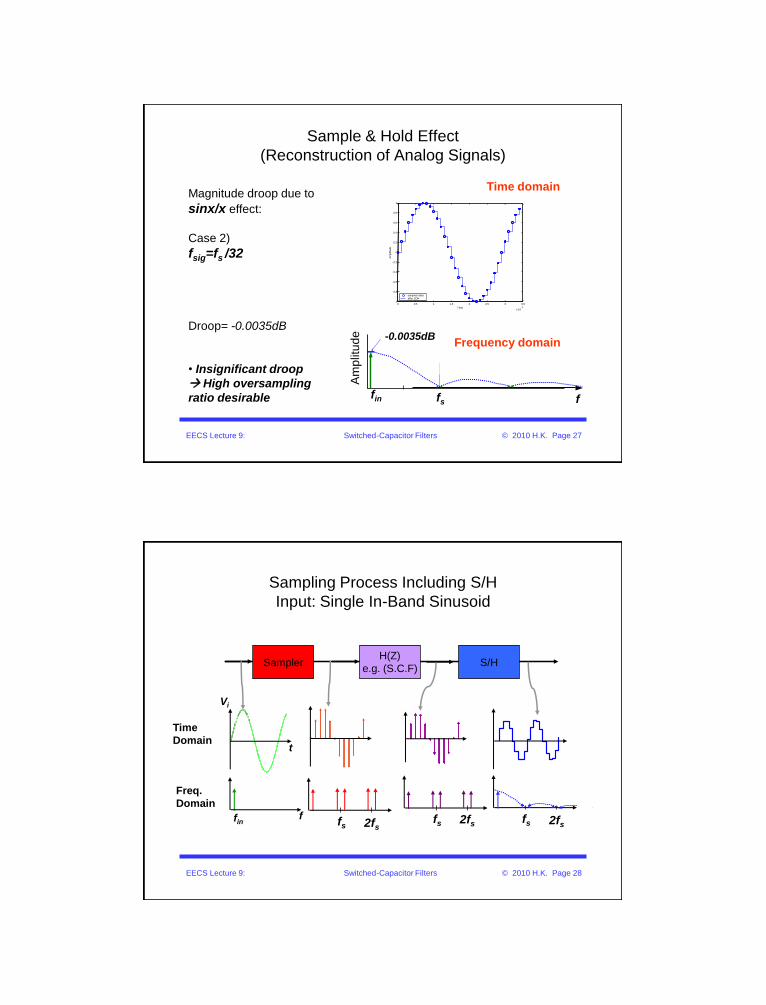
Sample & Hold Effect
(Reconstruction of Analog Signals)
Time domainMagnitude droop due to
sinx/x effect:
Case 2)
fsig=fs /32
Droop= -0.0035dB
• Insignificant droop
High oversampling
ratio desirable fs f
Am
plit
ud
e
fin
Frequency domain-0.0035dB
0 0.5 1 1.5 2 2.5 3 3.5
x 10-5
-1
-0.8
-0.6
-0.4
-0.2
0
0.2
0.4
0.6
0.8
1
Time
Am
plit
ude
sampled dataafter ZOH
EECS Lecture 9: Switched-Capacitor Filters © 2010 H.K. Page 28
Sampling Process Including S/H
Input: Single In-Band Sinusoid
fs
Time
Domain
2fs
t
Vi
Freq.
Domain
fs 2fsffin fs 2fs
SamplerH(Z)
e.g. (S.C.F)S/H

EECS Lecture 9: Switched-Capacitor Filters © 2010 H.K. Page 29
Sampling Process Including S/H
Input: In-Band Sinusoid + One Out-of-Band Sinusoid
fs 2fs
Freq.
Domain
fs 2fsffin1 fs 2fs
SamplerH(Z)
e.g. (S.C.F)S/H
fin2
Aliasing occurs prior to sinx/x shaping and hence sinx/x
effect does not attenuate aliased components
EECS Lecture 9: Switched-Capacitor Filters © 2010 H.K. Page 30
Sampling Process Including S/H
Input: General In-Band Signal
Vi
fs 2fsfB fs 2fs
fs 2fs
Freq.
Domain
General
Signal
SamplerH(Z)
e.g. (S.C.F)S/H
Beware of sinx/x shaping (droop) of in-band signals

EECS Lecture 9: Switched-Capacitor Filters © 2010 H.K. Page 31
1st Order Filter S.C. versus C.T.
Transient Analysis
SC response:
extra ½ clock cycle delay & steps
with finite rise time due to Rsw
1st Order RC versus SC LPF
fs = 1MHz
f-3dB=50kHz
fin= 3.6kHz
VIN
C2SC=1pF
VO_RC
C2RC=1pF
R1
3.2MegOHM
VO_SC
C1
314.2fF
S1 S2 Rsw
12
EECS Lecture 9: Switched-Capacitor Filters © 2010 H.K. Page 32
1st Order Filter
Transient Analysis
ZOH
• ZOH: Emulates an ideal S/H
pick signal after output is fully
settled
(usually at end of clock phase)
• Adds delay and sin(x)/x
shaping

EECS Lecture 9: Switched-Capacitor Filters © 2010 H.K. Page 33
Periodic AC Analysis
EECS Lecture 9: Switched-Capacitor Filters © 2010 H.K. Page 34
1st Order Filter
Magnitude Response
1.RC filter output
2.SC output after ZOH
3.Output after single
ZOH
4.S.C. filter output w/o
effect of ZOH
• (2) over (3)
• Repeats filter shape
around nfs• Identical to RC for
f << fs/2
1.RC filter
output
2,SC output
after ZOH
4.Corrected output
no ZOH
3.Sinc due to ZOH
fs 2fs 3fs

EECS Lecture 9: Switched-Capacitor Filters © 2010 H.K. Page 35
Periodic AC Analysis
• SPICE frequency analysis
–ac linear, time-invariant circuits
–pac linear, time-variant circuits
• SpectreRF statements
V1 ( Vi 0 ) vsource type=dc dc=0 mag=1
pacmag=1
PSS1 pss period=1u errpreset=conservative
PAC1 pac start=1 stop=1M lin=1001
• Output
–Divide results by sinc(f/fs) to correct for ZOH distortion
EECS Lecture 9: Switched-Capacitor Filters © 2010 H.K. Page 36
SpectreRF Circuit File
rc_pac
simulator lang=spectre
ahdl_include "zoh.def"
S1 ( Vi c1 phi1 0 ) relay ropen=100G rclosed=1 vt1=-500m vt2=500m
S2 ( c1 Vo_sc phi2 0 ) relay ropen=100G rclosed=1 vt1=-500m vt2=500m
C1 ( c1 0 ) capacitor c=314.159f
C2 ( Vo_sc 0 ) capacitor c=1p
R1 ( Vi Vo_rc ) resistor r=3.1831M
C2rc ( Vo_rc 0 ) capacitor c=1p
CLK1_Vphi1 ( phi1 0 ) vsource type=pulse val0=-1 val1=1 period=1u
width=450n delay=50n rise=10n fall=10n
CLK1_Vphi2 ( phi2 0 ) vsource type=pulse val0=-1 val1=1 period=1u
width=450n delay=550n rise=10n fall=10n
V1 ( Vi 0 ) vsource type=dc dc=0 mag=1 pacmag=1
PSS1 pss period=1u errpreset=conservative
PAC1 pac start=1 stop=3.1M log=1001
ZOH1 ( Vo_sc_zoh 0 Vo_sc 0 ) zoh period=1u delay=500n aperture=1n tc=10p
ZOH2 ( Vi_zoh 0 Vi 0 ) zoh period=1u delay=0 aperture=1n tc=10p

EECS Lecture 9: Switched-Capacitor Filters © 2010 H.K. Page 37
ZOH Circuit File
// Copy from the SpectreRF Primer
module zoh (Pout, Nout, Pin, Nin) (period,
delay, aperture, tc)
node [V,I] Pin, Nin, Pout, Nout;
parameter real period=1 from (0:inf);
parameter real delay=0 from [0:inf);
parameter real aperture=1/100 from (0:inf);
parameter real tc=1/500 from (0:inf);
{
integer n; real start, stop;
node [V,I] hold;
analog {
// determine the point when aperture
begins
n = ($time() - delay + aperture) / period
+ 0.5;
start = n*period + delay - aperture;
$break_point(start);
// determine the time when aperture ends
n = ($time() - delay) / period + 0.5;
stop = n*period + delay;
$break_point(stop);
// Implement switch with effective series
// resistence of 1 Ohm
if ( ($time() > start) && ($time() <=
stop))
I(hold) <- V(hold) - V(Pin, Nin);
else
I(hold) <- 1.0e-12 * (V(hold) - V(Pin,
Nin));
// Implement capacitor with an effective
// capacitance of tc
I(hold) <- tc * dot(V(hold));
// Buffer output
V(Pout, Nout) <- V(hold);
// Control time step tightly during
// aperture and loosely otherwise
if (($time() >= start) && ($time() <=
stop))
$bound_step(tc);
else
$bound_step(period/5);
}
}
EECS 247 Lecture 9 Switched-Capacitor Filters © 2010 H. K. Page 38
time
Vo
Output Frequency Spectrum prior to hold
fs 2fsf-3dB
First Order S.C. Filter
Vin Vout
C1
S1 S2
1 2
C2
Vin
time
Switched-Capacitor Filters problem with aliasing
|H(f)|

EECS 247 Lecture 9 Switched-Capacitor Filters © 2010 H. K. Page 39
time
Vo
Output Frequency Spectrum prior to hold
Antialiasing Pre-filter
fs 2fsf-3dB
First Order S.C. Filter
Vin Vout
C1
S1 S2
1 2
C2
Vin
time
Switched-Capacitor Filters problem with aliasing
Anti-Aliasing
Filter
EECS 247 Lecture 9 Switched-Capacitor Filters © 2010 H. K. Page 40
Sampled-Data Systems (Filters)
Anti-aliasing Requirements
• Frequency response repeats at fs , 2fs , 3fs…..
• High frequency signals close to fs , 2fs ,….folds back into passband (aliasing)
• Most cases must pre-filter input to sampled-data systems (filter) to attenuate signal at:
f > fs /2 (nyquist fmax < fs /2 )
• Usually, anti-aliasing filter included on-chip as continuous-time filter with relaxed specs. (no tuning)

EECS 247 Lecture 9 Switched-Capacitor Filters © 2010 H. K. Page 41
Antialiasing Pre-filter
fs 2fsf-3dB
Example : Anti-Aliasing Filter Requirements
• Voice-band CODEC S.C. filter high order low-pass with f-3dB =4kHz & fs =256kHz
• Anti-aliasing continuous-time pre-filter requirements:
– Need at least 40dB attenuation of all out-of-band signals which can alias inband
– Incur no phase-error from 0 to 4kHz
– Gain error due to anti-aliasing filter 0 to 4kHz < 0.06dB
– Allow +-30% variation for anti-aliasing filter corner frequency (no tuning) Need to find minimum required filter order
EECS 247 Lecture 9 Switched-Capacitor Filters © 2010 H. K. Page 42
Oversampling Ratio versus Anti-Aliasing Filter Order
2nd order Butterworth
Need to find minimum corner frequency for mag. droop < 0.06dB
Maximum Aliasing Dynamic Range
fs/fin_max
Filter Order
* Assumption anti-aliasing filter is Butterworth type
fs/fin =256K/4K=64

EECS 247 Lecture 9 Switched-Capacitor Filters © 2010 H. K. Page 43
Example : Meeting the Anti-Aliasing Filter Specifications
• Note that since the anti-aliasing filter is not tuned have to make sure all specifications are met under worst-case conditions
• Worst case passband droop occurs at narrowest possible anti-aliasing filter bandwidth
• Find the AA filter bandwidth for with droop <0.06dB
• Normalized frequency for 0.06dB droop: need perform passband simulation normalized =0.34
• Narrowest AA filter bandwidth4kHz/0.34=12kHz
0 0.05 0.15 0.25 0.35 0.45
-0.25
-0.2
-0.15
-0.1
-0.05
0
0.05
Normalized Frequency
Magnitude (
dB
)
0.06dB droop
EECS 247 Lecture 9 Switched-Capacitor Filters © 2010 H. K. Page 44
Example : Anti-Aliasing Filter Specifications• Since +-30% variation of AA
filter corner frequency is expected
• Set anti-aliasing filter corner frequency for minimum corner frequency 12kHz Find nominal corner frequency: 12kHz/0.7=17.1kHz
• Check if min. attenuation requirement is satisfied for widest filter bandwidth 17.1x1.3=22.28kHz
• Find (fs-fsig )/f-3dBmax
252/22.2=11.35make sure enough attenuation
• Check phase-error within 4kHz signal band for min. filter bandwidth via simulation
0 2 4 6 8 10 12
-40
-30
-20
-10
0
Normalized Frequency
Magnitude (
dB
)
-44dB

EECS 247 Lecture 9 Switched-Capacitor Filters © 2010 H. K. Page 45
Antialiasing Pre-filter
fs 2fsf-3dB
Example : Anti-Aliasing Filter
• Voice-band S.C. filter f-3dB =4kHz & fs =256kHz
• Anti-aliasing filter requirements:
– Need 40dB attenuation at clock freq.
– Incur no phase-error from 0 to 4kHz
– Gain error 0 to 4kHz < 0.06dB
– Allow +-30% variation for anti-aliasing corner frequency (no tuning)
2-pole Butterworth LPF with nominal corner freq. of 17kHz & no tuning (min.=12kHz & max.=22kHz corner frequency )
EECS 247 Lecture 9 Switched-Capacitor Filters © 2010 H. K. Page 46
Summary
• Sampling theorem fs > 2fmax_Signal
• Signals at frequencies nfS± fsig fold back down to desired signal band, fsig
This is called aliasing & usually mandates use of anti-aliasing pre-filters combined with oversampling
• Oversampling helps reduce required order for anti-aliasing filter
• S/H function shapes the frequency response with sinx/x shape
Need to pay attention to droop in passband due to sinx/x
• If the above requirements are not met, CT signals can NOT be recovered from sampled-data networks without loss of information

EECS 247 Lecture 9 Switched-Capacitor Filters © 2010 H. K. Page 47
Switched-Capacitor Network Noise
• During 1 high: Resistance of
switch S1 (RonS1) produces a
noise voltage on C with
variance kT/C (lecture 1- first
order filter noise)
• The corresponding noise
charge is:
Q2 = C2V2 = C2. kT/C = kTC
• 1 low: S1 open This
charge is sampled
vIN vOUT
C
S1 S2
1 2
RonS1
C
vIN
EECS 247 Lecture 9 Switched-Capacitor Filters © 2010 H. K. Page 48
Switched-Capacitor Noise
vIN vOUT
C
S1 S2
1 2
RonS2
C
• During 2 high: Resistance of
switch S2 contributes to an
uncorrelated noise charge on C
at the end of 2 : with variance
kT/C
• Mean-squared noise charge
transferred from vIN to vOUT per
sample period is:
Q2=2kTC
EECS 247 Lecture 9 Switched-Capacitor Filters © 2010 H. K. Page 49
• The mean-squared noise current due to S1 and S2’s kT/C noise is :
• This noise is approximately white and distributed between 0 and fs /2 (noise spectra single sided by convention) The spectral density of the noise is found:
S.C. resistor noise = a physical resistor noise with same value!
Switched-Capacitor Noise
2Q 2 2S ince i then i Qf 2k TCfs B st
22 2k TCfi B s 4k TCf B sf fs2
2 4k T1 i BSince R then : EQ f C f Rs EQ
EECS 247 Lecture 9 Switched-Capacitor Filters © 2010 H. K. Page 50
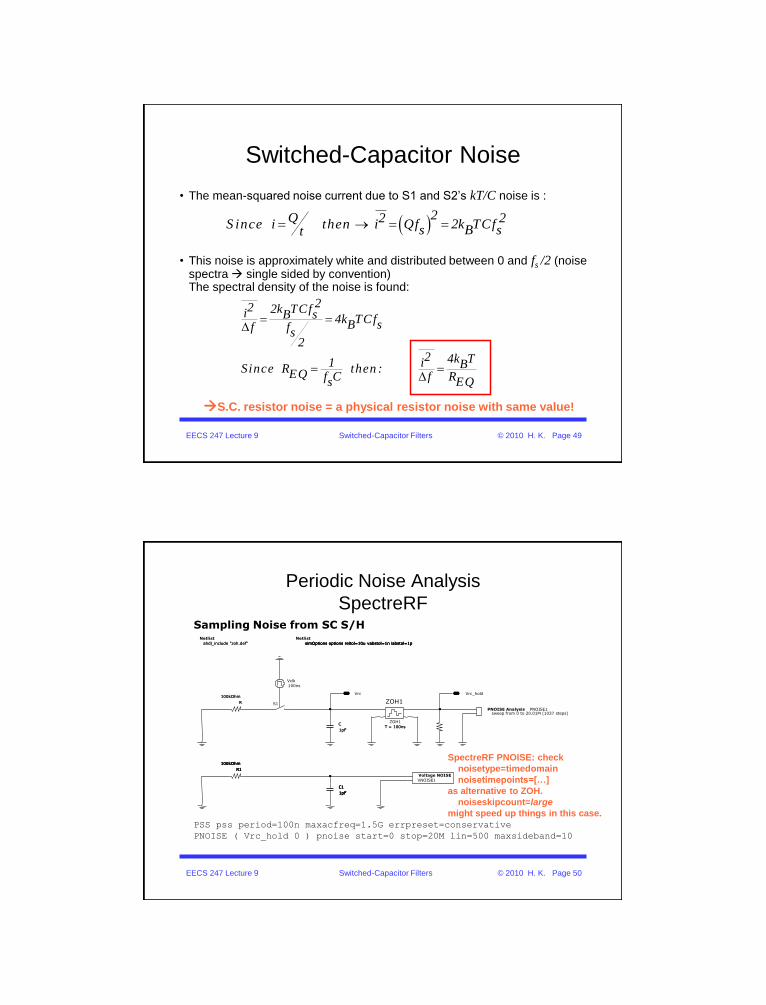
Periodic Noise Analysis
SpectreRF
PSS pss period=100n maxacfreq=1.5G errpreset=conservative
PNOISE ( Vrc_hold 0 ) pnoise start=0 stop=20M lin=500 maxsideband=10
SpectreRF PNOISE: check
noisetype=timedomain
noisetimepoints=[…]
as alternative to ZOH.
noiseskipcount=large
might speed up things in this case.
ZOH1
T = 100ns
ZOH1
T = 100ns
S1R
100kOhm
R
100kOhm
C
1pF
C
1pF
PNOISE Analysissweep from 0 to 20.01M (1037 steps)
PNOISE1
Netlist
ahdl_include "zoh.def"ahdl_include "zoh.def"
Vclk
100ns
Vrc Vrc_hold
Sampling Noise from SC S/H
C1
1pF
C1
1pF
C1
1pF
C1
1pF
R1
100kOhm
R1
100kOhm
R1
100kOhm
R1
100kOhm
Voltage NOISE
VNOISE1
Netlist
simOptions options reltol=10u vabstol=1n iabstol=1psimOptions options reltol=10u vabstol=1n iabstol=1psimOptions options reltol=10u vabstol=1n iabstol=1psimOptions options reltol=10u vabstol=1n iabstol=1p

EECS 247 Lecture 9 Switched-Capacitor Filters © 2010 H. K. Page 51
Sampled Noise Spectrum
Spectral density of sampled
noise including sinx/x effectNoise spectral density with
sinx/x effect taken out
V/s
qrt
(Hz)
No
rma
lize
d N
ois
e D
ensi
ty [
dB
]
EECS 247 Lecture 9 Switched-Capacitor Filters © 2010 H. K. Page 52
Total Noise
No
rmal
ized
To
tal
No
ise
v n
T/(
KT
/C)
1
0.1
fs /2
Sampled simulated noise
in 0 … fs/2: 62.2V rms
(expect 64V for 1pF)

EECS 247 Lecture 9 Switched-Capacitor Filters © 2010 H. K. Page 53
Switched-Capacitor Integrator
-
+
Vin
Vo
1 2
CI
Css
signal sampling
s0 I
s0 s
I
for f f
f CV V dtinC
Cf
C
-
+ 1
2
T=1/fs
Main advantage: No tuning needed
Critical frequency function of ratio of capacitors & clock freq.
EECS 247 Lecture 9 Switched-Capacitor Filters © 2010 H. K. Page 54
Switched-Capacitor Integrator
-
+
Vin
Vo
1 2
CI
Cs
-
+
Vin
Vo
1
CI
Cs
-
+
Vin
Vo
2
CI
Cs
1
2
T=1/fs
1 High
Cs Charged to Vin
2 High
Charge transferred from Cs to CI

EECS 247 Lecture 9 Switched-Capacitor Filters © 2010 H. K. Page 55
Continuous-Time versus Discrete-Time
Analysis Approach
Continuous-Time
• Write differential equation
• Laplace transform (F(s))
• Let s=j F(j)
• Plot |F(j)|, phase(F(j))
Discrete-Time
• Write difference equation relates output sequence to input sequence
• Use delay operator z -1 to transform the recursive realization to algebraic equation in z domain
• Set z= e jT
• Plot mag./phase versus frequency
o s i s
1o i
V ( nT ) V . . . . . . . . . .( n 1)T
V z V .. . . . . .z z
EECS 247 Lecture 9 Switched-Capacitor Filters © 2010 H. K. Page 56
Discrete Time Design Flow
• Transforming the recursive realization to algebraic
equation in z domain:
– Use delay operator z :
s1
s
1/ 2s
1s
1/ 2s
nT ..................... 1
............. z(n 1)T
.......... z(n 1/ 2 )T
............. z(n 1)T
.......... z(n 1/ 2 )T
* Note: z = e jTs = cos(Ts )+ j sin(Ts )

EECS 247 Lecture 9 Switched-Capacitor Filters © 2010 H. K. Page 57
Switched-Capacitor IntegratorOutput Sampled on 1
1 2 1 21
Vin
Vo
VCs
Clock
Vo1
-
+
Vin
Vo1
1 2 CI
Cs
1
Vo
EECS 247 Lecture 9 Switched-Capacitor Filters © 2010 H. K. Page 58
Switched-Capacitor Integrator
1 2 1 21
Vin
Vo
Vs
Clock
Vo1
F1 Qs [(n-1)Ts]= Cs Vi [(n-1)Ts] , QI [(n-1)Ts] = QI [(n-3/2)Ts]
F2 Qs [(n-1/2) Ts] = 0 , QI [(n-1/2) Ts] = QI [(n-1) Ts] + Qs [(n-1) Ts]
F1 _ Qs [nTs ] = Cs Vi [nTs ] , QI [nTs ] = QI[(n-1) Ts ] + Qs [(n-1) Ts]
Since Vo1= - QI /CI & Vi = Qs / Cs CI Vo1(nTs) = CI Vo1 [(n-1) Ts ] -Cs Vi [(n-1) Ts ]
(n-1)Ts nTs(n-1/2)Ts (n+1)Ts(n-3/2)Ts (n+1/2)Ts

EECS 247 Lecture 9 Switched-Capacitor Filters © 2010 H. K. Page 59
Switched-Capacitor Integrator
Output Sampled on 1
s
I
s
I
1s1I
o s o ss sI I inC
o s o s sinC
C1 1o o inC
CC 1
in
C V (nT ) C V C V(n 1)T (n 1)T
V (nT ) V V(n 1)T (n 1)T
V ( Z ) Z V ( Z ) Z V ( Z )
Vo Z( Z )ZV
DDI (Direct-Transform Discrete Integrator)
-
+
Vin
Vo1
1 2 CI
Cs
1
Vo
EECS 247 Lecture 9 Switched-Capacitor Filters © 2010 H. K. Page 60
z-Domain Frequency Response•Sampled-data systems z plane singularities analyzed via z-plane
•The s-plane j axis maps onto the unit-circle
•LHP singularities in s-plane map into inside of unit-circle in z-domain
•RHP singularities in s-plane map into outside of unit-circle in z-domain
•Particular values:
– f = 0 z = 1
– f = fs/2 z = -1
f = 0
f = fs /2
LHP in s-domain
imag. axis in
s-domain z-plane
z = e s.Ts

EECS 247 Lecture 9 Switched-Capacitor Filters © 2010 H. K. Page 61
z-Domain Frequency Response
• The frequency response is
obtained by evaluating H(z)
on the unit circle at:
z = e jT = cos(Ts) + j sin(Ts)
• Once z=-1 (fs /2) is reached,
the frequency response
repeats, as expected
• The angle to the pole is
equal to 360° (or 2
radians) times the ratio of
the pole frequency to the
sampling frequency
(cos(Ts),sin(Ts))
2f
fS
z-plane
EECS 247 Lecture 9 Switched-Capacitor Filters © 2010 H. K. Page 62
Switched-Capacitor Direct-Transform Discrete
Integrator
1s1I
s 1
I
CC 1
in
CC 1
Vo z( z )zV
z
-
+
Vin
Vo
1 2
CI
Cs
1

EECS 247 Lecture 9 Switched-Capacitor Filters © 2010 H. K. Page 63
DDI Integrator
Pole-Zero Map in z-Plane
z -1=0 z = 1
on unit circle
Pole from f 0
in s-plane mapped to z =+1
As frequency increases zdomain point moves on unit circle (CCW)
Once frequency gets to:
z=-1 (f=fs /2)
frequency response repeatsz-plane
f = fs /2
f
f1
1
(z-1)increasing
EECS 247 Lecture 9 Switched-Capacitor Filters © 2010 H. K. Page 64
DDI Switched-Capacitor Integrator
CI
Ideal Integrator Magnitude Error
1s s 11I I
j T / 2s sj T j T / 2 j T / 2I I
s
I
s
I
C C j TC C1 1
in
j jC C
C C1
C j T / 2C
C j T / 2C j T
Vo z( z ) , z ez zV
e ee1 since : sin2 je e e
1j e
2sin T / 2
T / 21 esin T / 2
-
+
Vin
Vo
1 2
CI
Cs
1

EECS 247 Lecture 9 Switched-Capacitor Filters © 2010 H. K. Page 65
DDI Switched-Capacitor Integrator
Example: Mag. & phase error for:
1- f / fs=1/12 Mag. error = 1% or 0.1dB
Phase error=15 degree
Qintg = -3.8
2- f / fs=1/32 Mag. error=0.16% or 0.014dB
Phase error=5.6 degree
Qintg = -10.2
CI
-
+
Vin
Vo
1 2
CI
Cs
1
DDI Integrator:
magnitude error no problem
phase error major problem
s
I
C j T / 2C j T
in
V T / 2o 1( z ) esin T / 2V
EECS 247 Lecture 9 Switched-Capacitor Filters © 2010 H. K. Page 66
5th Order Low-Pass Switched Capacitor Filter
Built with DDI Integrators
Example:
5th Order Elliptic Filter
Singularities pushed
towards RHP due to
integrator excess phase
s-plane
Fine View
j
s
Ideal Pole
Ideal Zero
s-plane
Coarse View
j
s
s
-s DDI Pole
DDI Zero

EECS 247 Lecture 9 Switched-Capacitor Filters © 2010 H. K. Page 67
Frequency (Hz)
Switched Capacitor Filter
Build with DDI Integrator jH
sf / 2 sf 2fs fContinuous-Time
Prototype
SC DDI based
Filter
Passband
Peaking
Zeros lost!
EECS 247 Lecture 9 Switched-Capacitor Filters © 2010 H. K. Page 68
Switched-Capacitor Integrator
Output Sampled on 2
CI
-
+
Vin
Vo2
1 2
CI
Cs
2
Sample output ½ clock cycle earlier
Sample output on 2
Vo

EECS 247 Lecture 9 Switched-Capacitor Filters © 2010 H. K. Page 69
F1 Qs [(n-1)Ts]= Cs Vi [(n-1)Ts] , QI [(n-1)Ts] = QI[(n-3/2)Ts]
F2 Qs [(n-1/2) Ts] = 0 , QI [(n-1/2) Ts] = QI [(n-3/2) Ts] + Qs [(n-1) Ts]
F1 _ Qs [nTs ] = Cs Vi [nTs ] , QI [nTs ] = QI[(n-1) Ts ] + Qs [(n-1) Ts]
F2 Qs [(n+1/2) Ts] = 0 , QI [(n+1/2) Ts] = QI [(n-1/2) Ts] + Qs [n Ts]
1 2 1 21
Vin
Vo2
Vs
Clock
(n-1)Ts nTs(n-1/2)Ts (n+1)Ts(n-3/2)Ts
Switched-Capacitor Integrator Output Sampled on 2
(n+1/2)Ts
EECS 247 Lecture 9 Switched-Capacitor Filters © 2010 H. K. Page 70
QI [(n+1/2) Ts] = QI [(n-1/2) Ts] + Qs [n Ts]
Vo2= - QI /CI & Vi = Qs / Cs CI Vo2 [(n+1/2) Ts] = CI Vo2 [(n-1/2) Ts ] -Cs Vi [n Ts ]
Using the z operator rules:
CI Vo2 z1/2 = CI Vo2 z
-1/2 - Cs Vi
1/ 2s1I
CC 1
in
Vo2 z( z )
zV
Switched-Capacitor Integrator Output Sampled on 2
1 2 1 21
Vin
Vo
Vs
Clock
(n-1)Ts nTs(n-1/2)Ts (n+1)Ts(n-3/2)Ts

EECS 247 Lecture 9 Switched-Capacitor Filters © 2010 H. K. Page 71
LDI Switched-Capacitor Integrator
1/ 2s1I
j T / 2s e s 1j T j T / 2 j T / 2I I
s
I
s
I
C j TC 1 z
in
C CC C1
CC
CC j T
Vo2 z( z ) , z e
V
e e e
1j
2 sin T / 2
T / 21sin T / 2
CI
Ideal Integrator Magnitude Error
No Phase Error!
For signals at frequencies << sampling freq.
Magnitude error negligible
-
+
Vin
Vo2
1 2
CI
Cs
2
LDI
LDI (Lossless Discrete Integrator)
same as DDI but output is sampled ½clock cycle earlier
EECS 247 Lecture 9 Switched-Capacitor Filters © 2010 H. K. Page 72
Switched-Capacitor Filter
Built with LDI Integrators jH
Zeros Preserved
Frequency (Hz) 2fs ffsfs /2


