Switch-mode Power Supply - College of Engineering Mode Power Supply.pdf · Switch-mode Power Supply...
19
Switch-mode Power Supply This laboratory exercise and its manual were originally designed and written by Prof. D. Lynch with contributions and revisions from M. Nesdoly, J. Kowalski, B. Fogal, A. El Damaty, Prof. S.B. Ko, and H. Majid. The manual was revised for EE321 by Prof. R. Johanson with input from P. Pourhaj and C. Janzen. Safety You should always follow safe procedures when working on any electronic circuit. Assemble or modify a circuit with the power off or disconnected. Don’t touch different nodes of a live circuit simultaneously, and don’t touch the circuit if any part of you is grounded. Don’t touch a circuit if you have a cut or sore that might come in contact with a live wire. Check the orientation of polarized capacitors before powering a circuit, and remember that capacitors can store charge after the power is turned off. Never remove a wire from an inductor while current is flowing through it. Components can become hot if a fault develops or even during normal operation so use appropriate caution when touching components. This laboratory exercise presents the following specific hazards: Shock: Inductors and transformers can produce very high potentials when the current through them is abruptly changed (usually by opening the circuit); allow for appropriate discharge paths and insulate yourself appropriately when contacting leads or components. A node connected to an inductor should be treated as possibly at a high voltage. Burn: Circuit elements under load, especially abnormal load caused by circuit or design errors, can reach temperatures which will cause burns to skin if contacted. Do not attempt to determine the temperature of elements with your fingers! Approach potentially overheated elements with caution and allow sufficient time for cooling when necessary. In some cases, elements may burst into flames. This is usually very isolated and does not normally create a fire hazard. If overheating does occur, immediately remove power and determine and correct the cause before re-energizing! Explosion: Capacitors that are subjected to potentials exceeding their rating can burst their cases. Polarized electrolytic capacitors commonly used as power supply filter elements can explode if they are connected with the polarity reversed, even below the rated voltage. Make certain that all electrolytic capacitors are connected with the proper polarity before energizing the circuit.
Transcript of Switch-mode Power Supply - College of Engineering Mode Power Supply.pdf · Switch-mode Power Supply...

Switch-mode Power Supply
This laboratory exercise and its manual were originally designed and written by Prof. D. Lynch with contributions and revisions from M. Nesdoly, J. Kowalski, B. Fogal, A. El Damaty, Prof. S.B. Ko, and H. Majid. The manual was revised for EE321 by Prof. R. Johanson with input from P. Pourhaj and C. Janzen.
Safety You should always follow safe procedures when working on any electronic circuit. Assemble or modify a circuit with the power off or disconnected. Don’t touch different nodes of a live circuit simultaneously, and don’t touch the circuit if any part of you is grounded. Don’t touch a circuit if you have a cut or sore that might come in contact with a live wire. Check the orientation of polarized capacitors before powering a circuit, and remember that capacitors can store charge after the power is turned off. Never remove a wire from an inductor while current is flowing through it. Components can become hot if a fault develops or even during normal operation so use appropriate caution when touching components. This laboratory exercise presents the following specific hazards: Shock: Inductors and transformers can produce very high potentials when the current through them is abruptly changed (usually by opening the circuit); allow for appropriate discharge paths and insulate yourself appropriately when contacting leads or components. A node connected to an inductor should be treated as possibly at a high voltage.
Burn: Circuit elements under load, especially abnormal load caused by circuit or design errors, can reach temperatures which will cause burns to skin if contacted. Do not attempt to determine the temperature of elements with your fingers! Approach potentially overheated elements with caution and allow sufficient time for cooling when necessary. In some cases, elements may burst into flames. This is usually very isolated and does not normally create a fire hazard. If overheating does occur, immediately remove power and determine and correct the cause before re-energizing! Explosion: Capacitors that are subjected to potentials exceeding their rating can burst their cases. Polarized electrolytic capacitors commonly used as power supply filter elements can explode if they are connected with the polarity reversed, even below the rated voltage. Make certain that all electrolytic capacitors are connected with the proper polarity before energizing the circuit.

Objectives: These experiments will investigate the operating principles and design of a switch-mode power supply (SMPS). At the end of the laboratory, a student should be able to
• explain the operation of a flyback circuit, • semi-quantitatively explain how the output voltage depends on switching frequency
and duty cycle, • explain the importance of incorporating a transformer in the design, and • design a simple switch-mode power supply that includes regulation.
Note: This design laboratory on switch-mode power supplies is independent of the lecture part of EE321 and is mostly self-contained. You are expected to read through the background material and understand the basic operation of a switch-mode power supply. You will then use the information to investigate the operation of sections of a SMPS and design a supply to certain specifications. The laboratory is in three parts; each part should be completed in a three hour laboratory period. The design part of the lab, part 3, requires that preparatory work be done before coming to the lab.1 The flyback circuit Introduction: The purpose of any d.c. voltage supply is to transform an unregulated, possibly varying voltage into a specified, stable voltage that is independent of the current drawn by the load (within limits, of course). There are various types of power supplies with the most common ones being the linear supply and the switch-mode power supply (SMPS). SMPSs have become the architecture of choice for power conversion because of their economy, high efficiency, and light weight. We begin this laboratory by investigating a core circuit in one type of SMPS without the complication of feedback regulation. The basic operating principles of a SMPS can be illustrated by the circuit in Fig. 1, which is called a flyback or inverting configuration. Let us analyze this circuit assuming all the components are ideal. The switch is repeatedly closed and opened at a frequency f with duty cycle η. During the first part of the cycle, the switch is closed, and the input voltage Vin is applied to the inductor. Recall that the fundamental equation for an inductor is V = L dI/dt. For a constant voltage applied to the inductor, the solution of this equation is a linear increase of the current with time, I = I0 + (Vin/L)t. Notice that the diode is reverse biased because of the polarity of the output voltage Vout. Meanwhile, on the other side of the circuit the capacitor supplies a current to the load resistor RL. This current will partially discharge the capacitor resulting in a decrease of Vout. The reverse-biased diode keeps the two parts of the circuit separate. When the switch opens, the inductor will attempt to keep the current flowing by very rapidly decreasing the voltage at node X. The voltage will continue to decrease until it reaches –Vout at which point the diode becomes forward biased. Current then flows through the diode and charges the capacitor resulting in an increase in Vout. The cycle then repeats. The current through the inductor and the voltage across the inductor are plotted in Fig. 2.
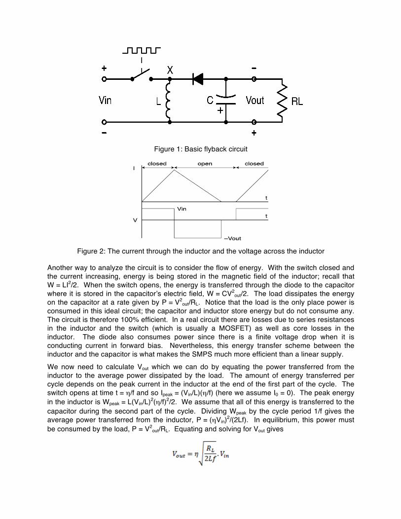
Figure 1: Basic flyback circuit
Figure 2: The current through the inductor and the voltage across the inductor
Another way to analyze the circuit is to consider the flow of energy. With the switch closed and the current increasing, energy is being stored in the magnetic field of the inductor; recall that W = LI2/2. When the switch opens, the energy is transferred through the diode to the capacitor where it is stored in the capacitor’s electric field, W = CV2
out/2. The load dissipates the energy on the capacitor at a rate given by P = V2
out/RL. Notice that the load is the only place power is consumed in this ideal circuit; the capacitor and inductor store energy but do not consume any. The circuit is therefore 100% efficient. In a real circuit there are losses due to series resistances in the inductor and the switch (which is usually a MOSFET) as well as core losses in the inductor. The diode also consumes power since there is a finite voltage drop when it is conducting current in forward bias. Nevertheless, this energy transfer scheme between the inductor and the capacitor is what makes the SMPS much more efficient than a linear supply. We now need to calculate Vout which we can do by equating the power transferred from the inductor to the average power dissipated by the load. The amount of energy transferred per cycle depends on the peak current in the inductor at the end of the first part of the cycle. The switch opens at time t = η/f and so Ipeak = (Vin/L)(η/f) (here we assume I0 = 0). The peak energy in the inductor is Wpeak = L(Vin/L)2(η/f)2/2. We assume that all of this energy is transferred to the capacitor during the second part of the cycle. Dividing Wpeak by the cycle period 1/f gives the average power transferred from the inductor, P = (ηVin)2/(2Lf). In equilibrium, this power must be consumed by the load, P = V2
out/RL. Equating and solving for Vout gives

Notice how the output voltage depends on the switching frequency and the duty cycle. Since these can be easily varied, they provide a means to set and regulate the output voltage. This calculation ignores the other power losses in a real circuit, but the formula is a useful simple approximation for working with the circuit.
The above calculation assumes that all the energy on the inductor is transferred each cycle, but is this true? Full transfer of energy will occur if the current through the inductor drops to zero before the end of the cycle. The time it takes for the current to drop from Ipeak to zero is given by the equation 0 = Ipeak – (Vout/L)t or t = IpeakL/Vout = (Vin/Vout)(η/f). This time must be less than the amount of time the switch is open (1–η)/f. This condition imposes a requirement on the duty cycle,
The calculation also assumes the output voltage is constant. Of course, if the power supply is designed properly, the output voltage should be nearly constant. However since the capacitor alternately receives and delivers charge, Vout must vary to some extent. The amount of the variation is called the ripple. We can estimate the magnitude of the ripple by calculating the discharge from the capacitor while the switch is closed. Since the diode is reverse biased, the capacitor is simply being discharged by the load resistance, and so the output voltage will decay as an exponential function with a time constant t = RLC. Since the ripple is expected to be small, we can linearize the exponential, Vout = Vmaxexp(-t/t) ~ Vmax(1–t/t). So at the end of the period with the switch closed, t = η/f, the voltage will have decreased by Vout(η/fRLC) which is the ripple
1.1 Some Practical Restrictions For proper operation of a switched-mode power supply, the inductor’s current must
• stay below saturation during switch ON time. The maximum ON time is
• drop to zero during switch OFF time. The maximum duty cycle to meet this requirement
is
: Inductor’s saturation current : Input DC voltage
: output voltage
The power is delivered to the inductor from DC input is
By rearranging the equation

If we assume there is no power loss in the circuit, the entire input power is delivered to the load. For a constant load and input voltage, the right side of above equation is constant. Fig. 3, shows a typical profile. Any point on between and can be used to deliver power to the load. Outside of this range, we exceed maximum values of or η and the inductor current is saturated.
Figure 3: η-Ton profile for a fixed load
Lowering the load resistance shifts the η-Ton profile to the right and the acceptable range becomes smaller, Fig. 4.
Figure 4: η-Ton profile for variable loads
The maximum power that can be delivered to the load without current saturation is
loadincreaseMaximumpower
validrange

1.2 Procedure Step 1 – Find restrictions
Measure actual inductance of inductor • Build the circuit according to Fig. 5 (use 50 Ω rheostat as load )
Calculate maximum duty cycle for Vin=25 Vdc and Vo=5±0.5 V • Measure inductor saturation current
o Monitor inductor current using voltage drop across 1Ω resistor o Apply a 10 KHz, 0-5 V square wave to the gate of MOSFET switch o Adjust duty cycle to reach saturation level ( ) o Make sure inductor current drops to zero during the switch OFF period o Calculate the maximum ON time
• Calculate maximum deliverable power and corresponding load current and load resistance
Step 2 – Constant frequency control • Calculate the switching frequency that delivers maximum power • Start with 50 Ω load, calculate the corresponding duty cycle • Test the circuit, do fine tuning if needed • Collect a few data points by increasing the load up to the maximum point, adjust η to
maintain correct output voltage
Step 3 – Constant ON time control • Use the ON time for maximum power • Start with 50 Ω load, calculate corresponding frequency and duty cycle • Test the circuit, do fine tuning if needed • Increase the load (lower the resistance), recalculate new switching parameters • Repeat the test to collect a few data points
Figure 5: Flyback circuit for measurements

Equations Comments
Total power delivered from input DC power source during the switch ON periods
Total power delivered by inductor during the switch OFF periods
Total power delivered to load
Peak inductor current at the end of ON period
Maximum switch ON time, for a specific input voltage
Assumption:
Higher duty cycles leave smaller OFF time to discharge inductor current completely and cause early inductor current saturation
Assumption:

2 Isolation A problem with the flyback circuit in Fig. 5 is that there is no isolation between the input voltage and the output voltage; failure of the diode could lead to a direct connection between input and output. If the input is derived directly from a.c. line voltages, there is a potential safety hazard. Replacing the inductor with a transformer is one way to achieve isolation as shown in Fig. 6. Another advantage of the isolation is that one side of the output can now be grounded.
Figure 6: Flyback circuit incorporating a transformer
The transformer must be of a special type that can work efficiently at higher frequencies (hundreds of KHz) and still transfer a respectable amount of power. The operation of this circuit is basically the same as the previous version. During the period when the switch is closed, current ramps up in the primary storing energy in the magnetic field. The linear increase in current causes a constant voltage to appear across the secondary, but this voltage reverse biases the diode (note the dots on the transformer), and the load current is supplied by the capacitor. When the switch opens the current falls in the primary inducing a voltage in the secondary that forward biases the diode. Current flows into the capacitor transferring the energy from the transformer to the capacitor. A simple power flow analysis of the circuit leads to the same equation for Vout (Is the inductance that of the primary or the secondary?). However, the transformer turns ratio between primary and secondary means that the voltages on the input side will differ from those of the output side. 2.1 Transformer Configuration For proper operation of SMPS with a transformer, similar to pervious section:
• During switch ON time, primary current must stay below saturation level:
• During switch OFF time, secondary current must drop to 0:
where n is the transformer turns ratio,

For switching parameters for any load less than the maximum load
Rearranging the above equations gives
: Maximum load power (design target)
2.2 Procedure Transformer configuration
• Input DC voltage: • Output voltage: • Output Power: • Measure actual inductance of all windings • Monitor saturation current
o Build a circuit according to Fig. 6 o Use 50Ω load o Use 1-3, 2-3, 4-5 as primaries and 12-13 for secondary o Explain your observation
• Find at least 3 transformer configuration with a proper turns ratio
Circuit test • Select one configuration and modify your circuit • Start with 50 Ω load, use constant frequency control to maintain output voltage up to
maximum load power. • Demonstrate working system to lab instructor

Equations Comments
Transformer Turns ratio
Total power delivered from input DC power source during switch ON periods
Total power delivered by inductor during switch OFF periods
Total power delivered to load
Peak inductor current at the end of ON period
Maximum switch ON time, for a specific input voltage
Assumption:
For a specific load, lower duty cycles cause inductor current saturated
Assumption:
Higher duty cycles leave smaller OFF time to discharge inductor current completely and cause early inductor current saturation

Snubber Circuits Parasiticelementsofpracticalcomponentoftencauseundesirableeffectsinelectronic/electricalsystems.InswitchingmodepowersuppliesitappearsasoscillationthatcancausedamagetoMOSFETswitches.Snubbercircuitsaredesignedtoreduceeffectsofcircuitoscillation.
ThissectionisbasedonapplicationnotesAN-4147andAN-11160.Itprovidestwodifferentapproachestodesignsnubbercircuits.Formoredetaildiscussionrefertooriginaldocuments.
SMPSwithPracticalElementsFigure1showsaFly-backconverterwithsomeofparasiticelementsthathavemajorroleincircuitoscillation.
Figure 1: Flyback converter with parasitic components
leakageinductorofprimarymagnetizedinductorofprimaryMOSFEToutputcapacitance
transformerratio
Whataretypicalvaluesfor , and ofthecomponentsinyourdesign?

OscillationWhentheMOSFETswitchisON,voltageacross isverylow.Whenitturnsoff,primarycurrentquicklycharges andincreasesdrain-sourcevoltage.When reachesto ,voltageacross
,is andsecondaryvoltageis .Secondarydiode, ,startsconducting.Outputcapacitor
clampsprimaryandsecondaryvoltagesatfixedlevels,Figure2.
Figure 2: Voltage levels when secondary diode starts conducting
Forcingvoltageacross toaDClevel,resemblesapplyingStepinputtotheLCoscillatorcomposedof
and ,thatcausesoscillation.Theoscillationfrequencyis:
Thevoltageondrainis:
TheoscillationcauseshighvoltagepeaksandovertimecancausedamagetotheMOSFET,Figure3.

Figure 3: Oscillations at primary side
CircuitDesign1.1.1 ParasiticelementsTodesignasnubbercircuit,firstweneedtodetermine and .
− Step 1: Find the resonance frequency after switch turns off ( ) − Step 2: Add a capacitor between drain and source − Step 3: Measure the new resonance frequency ( ) − Step 4: Use equation below to determine and
Are and intheacceptablerange?
1.1.2 RCSnubberCircuitByaddingaresistorandcapacitorbetweendrainandsource,wecreatesaRLCcircuitthatcandamptheoscillation,Figure4.

Figure 4: RC Snubber Circuit
ThestepresponseofaRLCcircuitisdepictedinFigure5.
Figure 5: Step response of RLC circuit
Foroverdampedoperation,ζmustbegreaterthan1.Highdampingfactorsmakecircuitmoresluggish.Sothereispracticallimitonhowlargeζcanbe.DampingfactorandcutofffrequencyfortheRLCisapproximatedusingfollowingequations:

Note:bothequationaresimplifiedforms. and arenotconsideredinequationsforDamping
factorandcutofffrequency.
• CircuitDesign
− Step 1: Select an initial value for ζ, calculate − Step 2: Select a cutoff frequency, calculate − Step 3: Test your circuit and change ζ and/or if required
1.1.3 RCDsnubberCircuitRCDsnubbercircuitprotectsMOSFETswitchfromovervoltagedamagebylimitingmaximumvoltagedropacrosstheswitch.Figure6showsRCDsnubbercircuitaddedtoprimarysideofthetransformer.Whendrainvoltageraisesto , conductsandprimarycurrentredirecttothesnubber
circuit. clampsdrainvoltageto .
Figure 6: Snubber circuit
Figure7showsdrainpinvoltageafterimplementingpropersnubbercircuit.
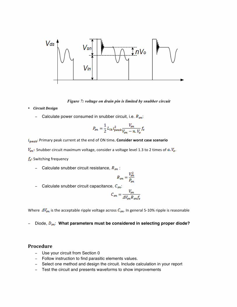
Figure 7: voltage on drain pin is limited by snubber circuit
• CircuitDesign
− Calculate power consumed in snubber circuit, i.e. :
PrimarypeakcurrentattheendofONtime.Considerworstcasescenario
Snubbercircuitmaximumvoltage,consideravoltagelevel1.3to2timesof .
Switchingfrequency
− Calculate snubber circuit resistance, :
− Calculate snubber circuit capacitance, :
Where istheacceptableripplevoltageacross .Ingeneral5-10%rippleisreasonable
− Diode, : What parameters must be considered in selecting proper diode?
Procedure− Use your circuit from Section 0 − Follow instruction to find parasitic elements values. − Select one method and design the circuit. Include calculation in your report − Test the circuit and presents waveforms to show improvements

Design of a regulated supply In previous parts, the circuit was not a regulated power supply since the output voltage changed with the load. A regulated supply will have additional circuitry that senses the output voltage and automatically adjusts the switching frequency or duty cycle to maintain a constant output. Semiconductor manufacturers have developed ICs that that perform SMPS regulation. Designhints
Error! Reference source not found. shows simplified block diagram of a regulated power supply (for the purpose of this lab).
Figure 8: Simplified block diagram of regulated power supply
• The step down transformer provides isolation for safety and reduces the AC voltage to 24V.
• The rectifier circuit rectifies the AC input, a half-wave or full-wave rectifier can be used for this stage.
• A filter capacitor is required to produce unregulated d.c. input voltage for next stage. The capacitance will determine the ripple on the unregulated voltage;
where I is the average current draw, and f is the frequency (60 Hz for half-wave and 120 Hz for full-wave rectification).
• The integrated regulator IC available to you is from STMicroelectronics’s UC384xB family, specifically the UC3845B.You will need to read the datasheet for the regulator IC. Yes, it is not very clear (actually the datasheet from ON Semiconductor is somewhat better than the one from STMicroelectronics). But datasheets are all too often poorly written, so this exercise is good practice.
1.1.4 ControllerchipThe controller regulates the voltage by adjusting the duty cycle at a fixed switching frequency which is a form of pulse width modulation (PWM). The controller computes the proper duty cycle based on two control loops; one that senses the current in the inductor (input pin 3) and one that senses the output voltage (input pin 2). Both of these feedbacks need to be wired for the chip to work. The computed PWM signal controls the switching MOSFET (output pin 6) (see Fig. 3-1).
step-downtransformer
rectifier/filter flyback circuit
controller IC
110V AC input
unregulated DC voltage
24V AC regulated DC
PWM signal voltage feedback
current feedback

Fig.3-1 Simplified internal block diagram of the controller
Figure 16 of datasheet (ON Semiconductor) shows the basic circuit for using the IC and includes connections to power, ground, the MOSFET, the current sense resistor, the voltage feedback, and an RC network to set the frequency. The current sense resistor generates a voltage proportional to the current through the inductor during the first part of the cycle (switch closed). The value of the sense resistor (Rs) must be selected such that Ipeak * Rs < 1.0 V. You can protect the current sense input with a voltage limiter (1.0 V zener diode). The voltage control compares the voltage feedback signal to a 2.5 V reference that is generated internally. The output voltage needs to be scaled to 2.5 V to provide the feedback signal. Scaling can be done using a simple voltage divider. The total resistance of the divider should be large enough to present a minimal additional load on the output. An internal oscillator controls the switching frequency; the oscillator’s frequency is set by an RC circuit connected to pins 4 and 8 (Figure 16 of the datasheet). Note that the switching frequency is half the internal oscillator’s frequency. The capacitor also controls the maximum duty cycle. OK so how do you choose R and C? You must decide on the switching frequency and maximum duty cycle based on the output voltage and maximum current draw by the load as you did in part 1. Then choose C to give the required maximum duty cycle based on the graph in Fig. 3 on page 4. Note that % output deadtime is the opposite of duty cycle, %DT = 1–η. Once you have C then choose R to give the correct oscillator frequency using the graph in Fig. 2 on page 4. If your resistor will be greater than 5K then you can instead use the formula below the graph in Fig. 2 to calculate R. Remember that the switching frequency is half the oscillator frequency.
+PWMGen.
error signal: current command
+
Error signal: duty cycle command.
+2.5V reference voltage
+
-
+
- current feedback
voltage feedback
Pin 6: PWM signal to control
power MOSFET
UC3845
Pin 3: current feedback input
current control loop voltage control loop
Pin 2: voltage feedback input

Important figure and tables (Datasheet from ON Semiconductor) • The PIN FUNCTION DESCRIPTION table on page 6 provides a brief but useful
description of UC3486B pins. • The MAXIMUM RATINGS table on page 2 must be considered during the design
process (e.g. the maximum voltage that can applied to the IC). • The Design Considerations section on page 9 provides some general design hints,
especially on how to use bypass capacitors for noise reduction. • Fig. 30 shows a better current feedback circuit where a RC filter is added to the current
sense input to eliminate narrow spikes on the leading edge of the current waveform. The spikes decrease the stability of the current control loop. For more details refer to the “Current Sense Comparator and PWM Latch” section on page 7.
1.1.5 DesignConstraintsAnotherrestrictionontransformerturnsratioenforcedbythecurrentcontrollerIC.UC3845cangeneratesquarewaveswithmaximum50%dutycycle,i.e.:
Rearrangingtheabovein-equationgives:
Thusthevalidrangeforturnsratiois:
Consider other maximum rating hat can affect your design.
ProcedureObjective: Design a 5V, 1W power supply. The output ripple must be less than 2%
− Input stage design: design rectifier module, find proper transformer configuration, and calculate input filter capacitor. How much ripple can the SMPS take at its input (tricky question)?
− Flyback circuit: Use flyback circuit with isolation in section 0, modify it to add current and voltage loops
− Controller module: calculate switching parameters, and design controller IC peripherals according to datasheet
− Design snubber circuit − Test each module independently whenever it is possible − Integrate all modules and test the complete circuit. Start with 50 Ω load, and increase the
load up to 1W − Demonstrate working system to lab instructor.