Surface plasmon resonances in periodic and random patterns ... · Surface plasmon resonances in...
12
Surface plasmon resonances in periodic and random patterns of gold nano-disks for broadband light harvesting Yoshiaki Nishijima, 1,∗ Lorenzo Rosa, 2 and Saulius Juodkazis 2,3 1 Department of Electrical and Computer Engineering, Graduate School of Engineering, Yokohama National University, 79-5 Tokiwadai, Hodogaya-ku, Yokohama 240-8501, Japan 2 Centre for Micro-Photonics, Faculty of Engineering and Industrial Sciences, Swinburne University of Technology, Hawthorn, VIC 3122, Australia 3 Melbourne Centre for Nanofabrication, 151 Wellington Road, Clayton, VIC 3168, Australia ∗ [email protected] Abstract: We analyze the localized surface plasmon resonance spectra of periodic square lattice arrays of gold nano-disks, and we describe numerically and experimentally the effect of disorder on resonance width, spectrum, and EM field enhancement in increasingly randomized patterns. The periodic structure shows a narrower and stronger extinction peak, conversely we observe an increase of up to (1 − 2) × 10 2 times enhancement as the disorder is gradually introduced. This allows for simpler, lower resolution fabrication, cost-effective in light harvesting for solar cell and sensing applications. We show that dipole-dipole interactions contribute to diffract light parallel to the surface as a mean of long-range coupling between the nano-disks. © 2012 Optical Society of America OCIS codes: (160.4236) Nanomaterials; (240.6680) Surface plasmons; (250.5403) Plasmon- ics; (290.4210) Multiple scattering; (220.4241) Nanostructure fabrication; (310.6628) Sub- wavelength structures, nanostructures. References and links 1. S. Link and M. A. El-Sayed, “Size and temperature dependence of the plasmon absorption of colloidal gold nanoparticles,” J. Phys. Chem. B 103, 4212–4217 (1999). 2. O. Shekhah, J. Liu, R. A. Fischer, and Ch. Woll, “MOF thin films: existing and future application,” Chem. Soc. Rev. 40, 1081–1106 (2011). 3. D. M. Koller, A. Hohenau, H. Ditlbacher, N. Galler, F. Reil, F. R. Aussenegg, A. Leitner, E. J. W. List, and J. R. Krenn, “Organic plasmon-emitting diode,” Nat. Photonics 2, 684–687 (2008). 4. W. Cai, A. P. Vasudev, and M. L. Brongersma, “Electrically controlled nonlinear generation of light with plas- monics,” Science, 333, 1720–1723 (2011). 5. A. E. Miroshnichenko, S. Flach, and Y. S. Kivshar, “Fano resonances in nanoscale structures,” Rev. Mod. Phys. 82, 2257–2298 (2010). 6. D. K. Gramotnev, A. Pors, M. Willatzen, and S. I. Bozhevolnyi, “Gap-plasmon nanoantennas and bowtie res- onators,” Phys. Rev. B 85, 045434 (2012). 7. V. K. Valev, N. Smisdom, A. V. Silhanek, B. De Clercq, W. Gillijns, M. Ameloot, V. V. Moshchalkov, and T. Verbiest, “Plasmonic ratchet wheels: switching circular dichroism by arranging chiral nanostructures,” Nano Lett. 9, 3945–3948 (2009). 8. M. Michaels, M. Nirmal, and L. E. Brus, “Surface enhanced raman spectroscopy of individual rhodamine 6G molecules on large Ag nanocrystals,” J. Am. Chem. Soc. 121, 9932–9939 (1999). 9. F. Lordan, J. H. Rice, B. Jose , R. J. Forster, and T. E. Keyes, “Site selective surface enhanced Raman on nanos- tructured cavities,” Appl. Phys. Lett. 99, 033104 (2011). #164456 - $15.00 USD Received 9 Mar 2012; revised 26 Apr 2012; accepted 27 Apr 2012; published 4 May 2012 (C) 2012 OSA 7 May 2012 / Vol. 20, No. 10 / OPTICS EXPRESS 11466
Transcript of Surface plasmon resonances in periodic and random patterns ... · Surface plasmon resonances in...

Surface plasmon resonances in periodicand random patterns of gold nano-disks
for broadband light harvesting
Yoshiaki Nishijima,1,∗ Lorenzo Rosa,2 and Saulius Juodkazis2,3
1Department of Electrical and Computer Engineering, Graduate School of Engineering,Yokohama National University, 79-5 Tokiwadai, Hodogaya-ku, Yokohama 240-8501, Japan
2Centre for Micro-Photonics, Faculty of Engineering and Industrial Sciences, SwinburneUniversity of Technology, Hawthorn, VIC 3122, Australia
3Melbourne Centre for Nanofabrication, 151 Wellington Road, Clayton, VIC 3168, Australia∗[email protected]
Abstract: We analyze the localized surface plasmon resonance spectraof periodic square lattice arrays of gold nano-disks, and we describenumerically and experimentally the effect of disorder on resonance width,spectrum, and EM field enhancement in increasingly randomized patterns.The periodic structure shows a narrower and stronger extinction peak,conversely we observe an increase of up to (1−2)×102 times enhancementas the disorder is gradually introduced. This allows for simpler, lowerresolution fabrication, cost-effective in light harvesting for solar cell andsensing applications. We show that dipole-dipole interactions contributeto diffract light parallel to the surface as a mean of long-range couplingbetween the nano-disks.
© 2012 Optical Society of America
OCIS codes: (160.4236) Nanomaterials; (240.6680) Surface plasmons; (250.5403) Plasmon-ics; (290.4210) Multiple scattering; (220.4241) Nanostructure fabrication; (310.6628) Sub-wavelength structures, nanostructures.
References and links1. S. Link and M. A. El-Sayed, “Size and temperature dependence of the plasmon absorption of colloidal gold
nanoparticles,” J. Phys. Chem. B 103, 4212–4217 (1999).2. O. Shekhah, J. Liu, R. A. Fischer, and Ch. Woll, “MOF thin films: existing and future application,” Chem. Soc.
Rev. 40, 1081–1106 (2011).3. D. M. Koller, A. Hohenau, H. Ditlbacher, N. Galler, F. Reil, F. R. Aussenegg, A. Leitner, E. J. W. List, and J. R.
Krenn, “Organic plasmon-emitting diode,” Nat. Photonics 2, 684–687 (2008).4. W. Cai, A. P. Vasudev, and M. L. Brongersma, “Electrically controlled nonlinear generation of light with plas-
monics,” Science, 333, 1720–1723 (2011).5. A. E. Miroshnichenko, S. Flach, and Y. S. Kivshar, “Fano resonances in nanoscale structures,” Rev. Mod. Phys.
82, 2257–2298 (2010).6. D. K. Gramotnev, A. Pors, M. Willatzen, and S. I. Bozhevolnyi, “Gap-plasmon nanoantennas and bowtie res-
onators,” Phys. Rev. B 85, 045434 (2012).7. V. K. Valev, N. Smisdom, A. V. Silhanek, B. De Clercq, W. Gillijns, M. Ameloot, V. V. Moshchalkov, and T.
Verbiest, “Plasmonic ratchet wheels: switching circular dichroism by arranging chiral nanostructures,” NanoLett. 9, 3945–3948 (2009).
8. M. Michaels, M. Nirmal, and L. E. Brus, “Surface enhanced raman spectroscopy of individual rhodamine 6Gmolecules on large Ag nanocrystals,” J. Am. Chem. Soc. 121, 9932–9939 (1999).
9. F. Lordan, J. H. Rice, B. Jose , R. J. Forster, and T. E. Keyes, “Site selective surface enhanced Raman on nanos-tructured cavities,” Appl. Phys. Lett. 99, 033104 (2011).
#164456 - $15.00 USD Received 9 Mar 2012; revised 26 Apr 2012; accepted 27 Apr 2012; published 4 May 2012(C) 2012 OSA 7 May 2012 / Vol. 20, No. 10 / OPTICS EXPRESS 11466

10. K. Ueno, S. Juodkazis, M. Mino, V. Mizeikis, and H. Misawa, “Spectral sensitivity of uniform arrays of goldnanorods to dielectric environment,” J. Phys. Chem. C 111, 4180–4184 (2007).
11. Y. Sawai, B. Takimoto, H. Nabika, K. Ajito, and K. Murakoshi “Observation of a small number of molecules ata metal nanogap arrayed on a solid surface using surface-enhanced Raman scattering,” J. Am. Chem. Soc. 129,1658–1662 (2007).
12. Y. Nishijima, K. Ueno, Y. Yokota, K. Murakoshi, and H. Misawa, “Plasmon-assisted photocurrent generationfrom visible to near-infrared wavelength using a Au-nanorods/TiO2 electrode,” J. Phys. Chem. Lett. 1, 2031–2036 (2010).
13. Y. Tsuboi, T. Shoji, N. Kitamura, M. Takase, K. Murakoshi, Y. Mizumoto, and H. Ishihara, “Optical trapping ofquantum dots based on gap-mode-extinction of localized surface plasmon,” Chem. Lett. 1, 2327–2333 (2010).
14. I. M. Monirul, K. Ueno, S. Juodkazis, Y. Yokota, and H. Misawa, “Development of interdigitated array electrodeswith surface-enhanced raman scattering Functionality,” Anal. Sci. 26, 13–18 (2010).
15. K. Ueno, S. Takabatake, K. Onishi, H. Itoh, Y. Nishijima, and H. Misawa, “Homogeneous nano-patterning usingplasmon-assisted photolithography,” Appl. Phys. Lett. 99, 011107 (2011).
16. J. Merlein, M. Kahl, A. Zuschlag, A. Sell, A. Halm, J. Boneberg, P. Leiderer, A. Leitenstorfer, and R. Brats-chitsch, “Nanomechanical control of an optical antenna,” Nat. Photonics 2, 230–233 (2008).
17. S. J. Barrow, A. M. Funston, D. E. Gomez, T. J. Davis, and P. Mulvaney, “Surface plasmon resonances in stronglycoupled gold nanosphere chains from monomer to hexamer,” Nano Lett. 11, 4180–4187 (2011).
18. A. Roberts, and L. Lin, “Substrate and aspect-ratio effects in resonant nanoaperture arrays,” Opt. Mater. Express1, 480–488 (2011).
19. K. Ueno, S. Juodkazis, V. Mizeikis, K. Sasaki, and H. Misawa, “Clusters of closely-spaced gold nanoparticles asa source of two-photon photoluminescence at visible wavelengths,” Adv. Mater. 20, 26–30 (2008).
20. T. Teranishi, M. Eguchi, M. Kanehara, and S. Gwo, “Controlled localized surface plasmon resonance wavelengthfor conductive nanoparticles over the ultraviolet to near-infrared region,” J. Mater. Chem. 21, 10238–10242(2011).
21. K. Ueno, S. Juodkazis, V. Mizeikis, K. Sasaki, and H. Misawa, “Spectrally-resolved atomic-scale length varia-tions of gold nanorods,” J. Am. Chem. Soc. 128, 14226–14227 (2006).
22. Y. K. Kim, A. J. Danner, J. J. Raftery, and K. D. Choquette, “Focused ion beam nanopatterning for optoelectronicdevice fabrication,” IEEE J. Sel. Top. Quantum. Electron. 11, 1292–1298 (2005).
23. M. Hu, C. Novo, A. Funston, H. Wang, H. Staleva, S. Zou, P. Mulvaney, Y. Xia, and G. V. Hartland, “Dark-fieldmicroscopy studies of single metal nanoparticles: understanding the factors that influence the linewidth of thelocalized surface plasmon resonance,” J. Mater. Chem. 18, 1949–1960 (2008).
24. S. Juodkazis, and L. Rosa, “Surface defect mediated electron hopping between nanoparticles separated by anano-gap,” Phys. Status Solidi - Rapid Res. Lett. 10, 244-246 (2010).
25. W. Khunsin, B. Brian, J. Dorfmuller, M. Esslinger, R. Vogelgesang, C. Etrich, C. Rockstuhl, A. Dmitriev, and K.Kern, “Long-distance indirect excitation of nanoplasmonic resonances,” Nano Lett. 11, 2765–2769 (2011).
26. M. I. Stockman, S. V. Faleev, and D. J. Bergman, “Localization versus delocalization of surface plasmons innanosystems: Can one state have both characteristics?” Phys. Rev. Lett. 87, 167401 (2001).
27. T. Takasone, S. Juodkazis, Y. Kawagishi, A. Yamaguchi, S. Matsuo, H. Sakakibara, H. Nakayama, and H. Mis-awa, “Flexural rigidity of a single microtubule,” Jpn. J. Appl. Phys. 41, 3015–3019 (2002).
28. T. Klar, M. Perner, S. Grosse, G. von Plessen, W. Spirkl, and J. Feldmann, ”Surface-plasmon resonances in singlemetallic nanoparticles,” Phys. Rev. Lett. 80, 4249–4252 (1998).
29. C. Sonnichsen, S. Geier, N. E. Hecker, G. von Plessen, J. Feldmann H. Ditlbacher, B. Lamprecht, J. R. Krenn,F. R. Ausseneg, V. Z-H. Chan, J. P. Spatz, and M. Moller, “Spectroscopy of single metallic nanoparticles usingtotal internal reflection microscopy,” Appl. Phys. Lett. 77, 132355, (2000).
30. M. L. Brongersma, J. W. Hartman, and H. A. Atwater, “Electromagnetic energy transfer and switching innanoparticle chain arrays below the diffraction limit,” Phys. Rev. B 62, R16356–R16359 (2000).
31. B. Lamprecht, G. Schider, R. T. Lechner, H. Ditlbacher, J. R. Krenn, A. Leitner, and F. R. Aussenegg, “Metalnanoparticle gratings: Influence of dipolar particle interaction on the plasmon resonance,” Phys. Rev. Lett. 84,4721–4724 (2000).
32. W. Gotschy, K. Vonmetz, A. Leitner, and F. R. Aussenegg, “Optical dichroism of lithographically designed silvernanoparticle films,” Opt. Lett. 21, 1099–1101, (1996).
33. C. Sonnichsen, T. Franzl, T. Wilk, G. von Plessen, J. Feldmann, O. Wilson, and P. Mulvaney, “Drastic reductionof plasmon damping in gold nanorods,” Phys. Rev. Lett. 88, 077402 (2002).
34. G. V. Hartland, “Coherent vibrational motion in metal particles: Determination of the vibrational amplitude andexcitation mechanism,” J. Chem. Phys. 116, 8048–8056 (2002).
35. L. Rosa, K. Sun and S. Juodkazis, “Sierpinski fractal plasmonic nanoantennas,” Phys. Status Solidi - Rapid Res.Lett. 5, 175–177 (2011).
36. X. Chen, B. Jia, J. K. Saha, B. Cai, N. Stokes, Q. Qiao, Y. Wang, Z. Shi and M. Gu, “Broadband enhance-ment in thin-film amorphous silicon solar cells enabled by nucleated silver nanoparticles,” Nano Lett. 2012 doi:10.1021/nl203463z (in press)
37. K. Aydin, V. E. Ferry, R. M. Briggs, and H. A. Atwater,“Broadband polarization-independent resonant light
#164456 - $15.00 USD Received 9 Mar 2012; revised 26 Apr 2012; accepted 27 Apr 2012; published 4 May 2012(C) 2012 OSA 7 May 2012 / Vol. 20, No. 10 / OPTICS EXPRESS 11467

absorption using ultrathin plasmonic super absorbers,” Nat. Commun. 2, 517 (2011).38. A. K. Sarychev, V. A. Shubin, and V. M. Shalaev, “Anderson localization of surface plasmons and nonlinear
optics of metal-dielectric composites,” Phys. Rev. B 60 16389–16408 (1999).39. S. Takeda, S. Hamada, R. Peretti, P. Viktorovitch, and M. Obara, “ Order to disorder optical phase transition in
random photonic crystals,” Appl. Phys. B 106 95–100 (2012).40. Z. -L. Deng, Z. -H. Li and J. -W. Dong, and H. -Z. Wang, “In-plane plasmonic modes in a quasicrystalline array
of metal nanoparticles,” Plasmonics 6, 507-514 (2011).41. K. Juodkazis, J. Juodkazyte, P. Kalinauskas, E. Jelmakas, and S. Juodkazis, “Photoelectrolysis of Water: Solar
Hydrogen - Achievements and Perspectives,” Opt. Express 18, A147–A160 (2010).
1. Introduction
Localized surface plasmons are generated in nanostructures of noble metals such as gold, sil-ver and copper, which are promising materials in the fields of optoelectronics and plasmon-ics [1–6]. Recently, their applications have been widely examined and reported. For instance,detection of small amounts of molecules by surface enhanced Raman scattering (SERS) spec-troscopy [7–10], refractive index sensing [10], nanolithography [11], solar energy harvesting atwavelength of choice [12], optical trapping [13] and electrochemistry [14] are several active di-rections of research. In particular, short-range plasmon resonances in so-called “nano-gaps” [6]have been discussed because of their strong electric field enhancement (|E|2 ∼ 104) [15, 16].Fabrication of gold nano-structures is mainly accomplished either by chemical synthesis or bysemiconductor nano-fabrication methods [16–23]. Because of the difficulty to control the parti-cle size distribution, and immobilizing them on a substrate, most of colloidal particle work hasbeen done with random configurations.
On the other hand, nano-fabrication often involves fabricating periodic structures, becauseof their convenience for CAD design and numerical benchmarking with simulations using thefinite-difference time-domain (FDTD) method. With nano-fabrication it is easy to control theparticle size and their periodicity, hence, spectral patterns of light absorption and scattering,enhancement at nano-gaps, peculiarities of dipole-dipole interaction, and optical nonlinearitiesof localized surface plasmons (LSPRs) have been demonstrated and explored [6,19]. However,the facility costs are increasing when fabrication resolution of nano-gaps down to few nanome-ters is required. Moreover, the required high-voltage (≥ 100 keV) electron beam lithographyis known to create subsurface defects [24] and, e.g., can compromise performance and longtime stability of solar cells. One strongly desired feature is a large enhancement factor with lowfabrication resolution (leading to low-cost device fabrication as a result).
In this study, we show long-range interactions during the transition between order and dis-order in low-resolution fabricated gold nano-particles, and the transition effect on the opticalproperties of such patterns. Dipole-dipole long-range interactions between perfectly orderednano-particle arrays [31] and fully disordered [25, 26] patterns of plasmonic nano-particleshave been examined. The ordered patterns show distinct extinction resonances scalable withthe period and spectrally red-shifted, because of the phase alignment of scattered fields betweenneighboring particles [31]. In disordered patterns it is shown that the dipole-dipole interactionvirtually disappears when Period/Diameter > 2.5 [25]. Here, we show how by tuning the de-gree of randomness it is possible to control the extinction properties of the patterns, through thestrong dipolar interactions arising from the shift between evanescence and radiation of differentlight diffraction orders. The long-range interaction of nano-particles observed in the extinctionspectrum is maximum at the critical period, when diffraction orders radiates and higher ordersare traveling along the surface in a grazing angle mode. The optical properties (extinction spec-tra and field enhancement) of gold nano-disk arrays are systematically studied experimentallyand numerically for the first time during the order-to-disorder evolution, which is introduced ina controlled way through a random walk algorithm.
#164456 - $15.00 USD Received 9 Mar 2012; revised 26 Apr 2012; accepted 27 Apr 2012; published 4 May 2012(C) 2012 OSA 7 May 2012 / Vol. 20, No. 10 / OPTICS EXPRESS 11468

Initial point
Movable area
Periodic arrangement Random arrangement
N = 0 N = 1 N = 2
(a)
(b)
0 200 400 600 800 10000
500
1000
1500
2000
Coun
ts
Random walk distance (nm)
Random walking
Random walk distance
Fig. 1. (a) Method description for random configuration preparation. (b) Statistical distribu-tion of nano-disk distance from the initial configuration, from the first to tenth random-walkstep (a numerical result).
2. Samples and methods
Patterns of gold nano-disks are CAD generated by the random-walk method starting from aperfectly periodic arrangement. A schematic illustration of the random structure preparation isshown in Fig. 1(a), where the centers of the disks are allowed to move up to 150 nm beyondthe disk diameter for each step, and the random walk is iterated for N = 10 steps. The statisticaldistribution of the step-by-step nano-disks’ distances from the initial configuration is shown inFig. 1(b), where the random-walk distances are well fit by Gaussian profiles with average dis-tance increasing with the step number. Random walks have been generated for initial periodic-ities ranging from 450 nm to 800 nm, with disks diameters of d = 150, 200, and 250 nm. Afterthe final random walk step, the area covered by the nano-disks is expanded by about 0.17%,and 1% of the disks overlap (which is allowed by the algorithm design); correspondingly, thegold area coverage decreases by 1.01 times.
The arrays have been fabricated by electron beam (EB) lithography lift-off techniques. EBresist (ZEP520A, Zeon) has been coated on glass substrate by spin coating (3000 rpm, 60 s).After baking at 180◦C for 2 min., the surface of resist has been coated with charge dissipatingagent for EB lithography (ESPACER, Showa Denko). The EB drawing has been carried out
#164456 - $15.00 USD Received 9 Mar 2012; revised 26 Apr 2012; accepted 27 Apr 2012; published 4 May 2012(C) 2012 OSA 7 May 2012 / Vol. 20, No. 10 / OPTICS EXPRESS 11469
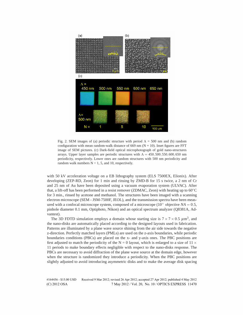
Fig. 2. SEM images of (a) periodic structure with period Λ = 500 nm and (b) randomconfiguration with mean random-walk distance of 669 nm (N = 10). Inset figures are FFTimage of SEM pictures. (c) Dark-field optical microphotograph of gold nano-structuresarrays. Upper layer samples are periodic structures with Λ = 450,500,550,600,650 nmperiodicity, respectively. Lower ones are random structures with 500 nm periodicity andrandom walk numbers N = 1, 5, and 10, respectively.
with 50 kV acceleration voltage on a EB lithography system (ELS 7500EX, Elionix). Afterdeveloping (ZEP-RD, Zeon) for 1 min and rinsing by ZMD-B for 15 s twice, a 2 nm of Crand 25 nm of Au have been deposited using a vacuum evaporation system (ULVAC). Afterthat, a lift-off has been performed in a resist remover (ZDMAC, Zeon) with heating up to 60◦Cfor 3 min., rinsed by acetone and methanol. The structures have been imaged with a scanningelectron microscope (SEM - JSM-7500F, JEOL), and the transmission spectra have been meas-ured with a confocal microscope system, composed of a microscope (10× objective NA = 0.5,pinhole diameter 0.1 mm, Optiphoto, Nikon) and an optical spectrum analyzer (Q8381A, Ad-vantest).
The 3D FDTD simulation employs a domain whose starting size is 7× 7× 0.5 μm3, andthe nano-disks are automatically placed according to the designed layouts used in fabrication.Patterns are illuminated by a plane wave source shining from the air side towards the negativez-direction. Perfectly matched layers (PMLs) are used on the z-axis boundaries, while periodicboundaries conditions (PBCs) are placed on the x- and y-axis ones. The PBC positions arefirst adjusted to match the periodicity of the N = 0 layout, which is enlarged to a size of 11×11 periods to make boundary effects negligible with respect to the nano-disks response. ThePBCs are necessary to avoid diffraction of the plane wave source at the domain edge, howeverwhen the structure is randomized they introduce a periodicity. When the PBC positions areslightly adjusted to avoid introducing asymmetric disks and to make the average disk spacing
#164456 - $15.00 USD Received 9 Mar 2012; revised 26 Apr 2012; accepted 27 Apr 2012; published 4 May 2012(C) 2012 OSA 7 May 2012 / Vol. 20, No. 10 / OPTICS EXPRESS 11470

Fig. 3. (a) Schematic depiction of extinction measurements and coupling of diffracted lightalong surface via radiation at grazing angle. (b) Photos of the diffraction pattern in trans-mission, 2nd-order is in grazing mode and propagates along the surface (recognizable bycoloring of the cover glass edges).
uniform, their influence has been found negligible due to the large number of disks includedin the domain. The reflected and transmitted power is collected by two monitors at oppositeends of the domain; due to the periodicity, the monitors collect the total power over all thediffraction orders. The effect of staircase approximation is addressed by reducing the squaremesh size around the nano-disks to about 2 nm (or about λ/500), forcing the use of a dedicatedmachine on a 3D mesh totaling around 1.5 million mesh points. The simulation times rangedfrom 1 to 3 hours and total memory occupancy ranged from 10 to 18 GB, with increasingtimes and memory according to greater mesh complexity for increasing random-walk step. Thesimulations have been performed on the Green machine, a 150-node supercomputer with 8-corecalculation nodes, each carrying 16 GB memory. Workload has been subdivided by employingone 8-node cluster per simulation.
3. Results and discussion
3.1. Optical properties and grating coupling
Figures 2(a) and 2(b) show SEM images of fabricated gold nano-disks together with their 2Dfast Fourier transform (FFT) spatial distributions in the insets. With respect to the periodicstructures, the random structures for N = 10 have clearly lost their periodicity. The FFT retainsperiodicity peaks up to third order for N = 0, 1, and 2, while for greater number of steps onlyzero- and first-order peaks remain, indicating a randomness increase of the disk array for in-creasing step N, although weak periodic features persist even after many steps. After severalsteps, some of the nano-disks start to cluster within a few nanometers or overlap, a situationthat models well the aggregates reached by self-assembling nano-particles, typically obtainedin experiments of chemical gold nano-particle synthesis. These features are also revealed bydark-field optical imaging, a scattering measurements technique for single nano-particle spec-troscopy [19, 23, 27–29]. Although the nano-disk extinction spectra peak in the near-infrared(see Figs. 3 and 4(a)), scattering peaks in the visible band, ranging from blue to red color. Sincein the dark field imaging only the scattered light is collected (transmission is not detected) theperiodic array of gold nano-disks act as a diffraction grating and only the color of the diffractedlight is apparent in the image; strong scattering occurs at wavelengths close to wavelength of
#164456 - $15.00 USD Received 9 Mar 2012; revised 26 Apr 2012; accepted 27 Apr 2012; published 4 May 2012(C) 2012 OSA 7 May 2012 / Vol. 20, No. 10 / OPTICS EXPRESS 11471

light. On the other hand, the scattering color becomes gradually blurred with increasing stepN and increase of randomness (bottom row in Fig. 2(c)). The N = 5 and N = 10 dark-field im-ages show a slightly reddish color, with a white background. The red color corresponds to thegold plasmonic resonance, and the white color is due to multi-wavelength distributed scatteringcaused by the randomness.
Figure 3 shows schematically how the higher order diffraction is coupled into light directedalong the surface at grazing angle in case of critical period Λ. The experimentally measured1st-order diffraction angles, Θ±1, are shown in Fig. 3(b). It is noteworthy that in the case ofoptically thick not plasmonic pattern, the diffraction orders would gradually disappear in trans-mission as the period becomes small and closer to the wavelength of incident light accordingto the grating formula nλ = ΛsinΘn, here n is the order of diffraction maxima, Λ is the period,and λ is the wavelength of incident light. Since gold cylinders are only 40-nm-thick and trans-mission is mediated by plasmons, an efficient diffraction in transmission has been observed(Fig. 3(b)). The 2nd-order diffraction is exactly at grazing angle; it directs light along the sur-face and contributes to surface plasmon excitation along the array of Au-cylinders [30]. Thiscontributes to the light enhancement by individual nano-disks. In this way even far away sepa-rated nano-disks are coupled at specific wavelengths when diffraction enters grazing mode; anextinction spectrum shows the corresponding peak. The 1st-order diffraction also contributes tothe extinction losses (see, Fig. 3(a)) but it does not contribute to the light enhancement sincelight is escaping surface and nano-particles. Light propagation from glass to air is favorable forgrazing angle coupling. For the quantitative results, the electromagnetic field enhancement isestimated by FDTD analysis in Sec. 3.3.
3.2. Experimental extinction spectra
The plasmonic resonances of the periodic/random structures have been characterized bymeasuring their extinction spectra for periodicity intervals between 450 and 800 nm, and diskdiameters from 150 to 250 nm, in 50 nm intervals. Typical extinction spectra of periodic arraysare shown in Fig. 4. With increasing periodicity, the extinction peak value decreases, as thedensity of gold nano-disks decreases, and the peak wavelength is red-shifted. As for the causeof this red-shift, the near-field coupling of gold nano-particles pairs is efficient at few tensnanometers distance and gradually vanishes as Λ/d > 2.5 [25]. The red shift (Fig. 4) showsthat dipole-dipole interaction is stronger as the separation between the particles increases in theperiodic pattern [25]. In fact, as observed in FDTD calculations, at the particular wavelength,the electromagnetic field enhancement also increases (see, Sec. on simulations). According torefs. [25,31,32], the red shift is related to the dipole-dipole interaction, is linked to the phase ofplasmonic field, and its strength can be estimated from the bandwidth of plasmonic resonance.The results shown in Fig. 4 for the periodic patterns are in good agreement with predictionsreported in ref. [31] for the longer wavelengths (emission to air [31]). At the shorter wave-lengths, the feature at critical period [31] due to coherent plasmon scattering and emission intosubstrate was out of spectral range of our detection (Fig. 4), but can be recognized in Figs. 2(c)and 3 when propagating diffraction orders forms the image and recognizable by color of theextinction maxima (direct transmission is canceled in the dark-field microscopy mode).
The difference between periodic and random arrays is analyzed in Fig. 5(a), where therandom-walk effect on the spectra causes linearly decreasing extinction peak values with in-creasing average random-walk distance, with a blue-shift of the peak wavelength as the in-phase matching of the scattered fields of the single nano-particles is progressively disrupted(see Fig. 5(b)). Extinction wavelengths are almost the same in all samples. This result indi-cates that the quality Q-factor of the random arrays is strongly linked to that of the periodicones. It is noteworthy that what we discuss further in terms of the Q-factor and dephasing time,
#164456 - $15.00 USD Received 9 Mar 2012; revised 26 Apr 2012; accepted 27 Apr 2012; published 4 May 2012(C) 2012 OSA 7 May 2012 / Vol. 20, No. 10 / OPTICS EXPRESS 11472

600 800 1000 1200 1400 1600
0.0
0.1
0.2
0.3
0.4
Extin
ction
Wavelength (nm)
Period 450 nm500 nm550 nm600 nm650 nm700 nm
Fig. 4. Experimental extinction spectra of periodic arrays with periods between Λ= 450 nmand 700 nm. Diameter of nano-cylinders d = 150 nm.
T2 (defined by the FWHM of the extinction peak) are affected by diffraction losses (Fig. 3).Hence, a strong and narrow extinction peak (consequently large T2) does not necessary meanthat nano-particles are less interacting, but rather contribute to strong diffraction (e.g., Fig. 5(b))as discussed below.
The dephasing time of the plasmon resonance T2 = 2h /Γ, where Γ is the FWHM of the res-onance peak [33, 34] and h is the reduced Planck constant. Results are plotted in Fig. 5(b) asa function of the average random-walk distance, that is the maximum peak of the Gaussian fitin Fig. 1(b): the dephasing time is inversely proportional to the average distance. Therefore,the FWHM of extinction resonance is linearly increasing as random walk progresses, however,the area under the extinction curve is almost constant, with a linear reduction of the observedextinction maximum. Interestingly, all the random structures converge towards the same de-phasing time T∞ = 3.7 fs (defined as the dephasing time at N = ∞, or the time in completelyrandom patterns). On the other hand, the periodic dephasing time varies considerably with theperiod, as can be seen from appearance in Fig. 3. The dephasing is related to the LSPR lossesdue to interaction between nano-particles in the pattern as well as due to diffraction. By con-trolling the average intra-particle distance is it possible to tune the width of the extinction peak.
We also performed dephasing measurements on the samples with different nano-disk diam-eters. The ratio of dephasing time between periodic and random (at N = ∞) arrays has beenplotted in Fig. 6: the maximum dephasing time is strongly linked to the square lattice pe-riod. There is an optimal period for each disk diameter: for 150 nm diameter it is 550 nm,for 200 nm diameter it is 650 nm, and for 250 nm diameter it is 750 nm, respectively. Note,those wavelengths corresponds to strong diffraction responsible for the scattered/diffracted lightin dark-field imaging (see, Fig. 2(c)) and are explained by the discussed mechanism shown inFig. 3(a). This value is connected to the LSPR wavelength, namely, when the LSPR wavelengthhas shifted to longer wavelength because of the increasing disk diameter, the diffraction lossesdue to effective grating also shifts to longer wavelengths (Fig. 1(b)). As a result, the extinctionvalue, Q-factor, and dephasing time, T2, measured spectroscopically have maxima related to theplasmonic properties as well as to the light diffraction losses due to pattern periodicity.
In the case of a random structure, each nano-disk has slightly different resonance wavelengthbecause of different long-range interaction, thus the randomly-scattered light is spread over allwavelengths, as shown in Fig. 2(c) and LSPR spectra seem to have broader and lower extinctionand shorter dephasing time. Spectrally broader plasmon resonances are favorable in practical
#164456 - $15.00 USD Received 9 Mar 2012; revised 26 Apr 2012; accepted 27 Apr 2012; published 4 May 2012(C) 2012 OSA 7 May 2012 / Vol. 20, No. 10 / OPTICS EXPRESS 11473

Fig. 5. Random-walk induced changes of experimentally measured extinction; diameter ofnano-disk is d = 150 nm. (a) Extinction spectra for Λ = 550 nm with N = 0, 3, 5, and10, respectively. (b) Dependence of the extinction maximum and of the dephasing time, T2(extinction at peak wavelength) on the random-walk distance.
Fig. 6. Experimental dephasing time ratios of periodic structures relative to random struc-tures for different diameters d = 150 (1), 200 (2), and 250 nm (3), respectively.
light harvesting applications [35–37]. In contrast, periodic nano-disk arrays show an increase ofthe LSPR resonance, relative to the random configuration, larger Q-factor and longer dephasingtime T2 (Fig. 6).
3.3. 3D-FDTD analysis of light field enhancement
Field enhancement calculation is then confirmed by simulation with 3D-FDTD softwareLumerical, looking for extinction and E-field enhancement values around the peak wavelength.Calculation has been performed on a 6 ×6 μm wide domain for the periodic ordered and ran-dom structures with disks’ arrangement as taken from the CAD design. The arrays are illumi-nated by a x-polarized plane wave source between 600 and 1000 nm wavelength. The periodicarray shown in Fig. 7(b) has periodicity of 600 nm and nano-disk diameter of 160 nm (the de-signed diameter was d = 150 nm). It can be seen in Fig. 7(a) that the maximum extinction is
#164456 - $15.00 USD Received 9 Mar 2012; revised 26 Apr 2012; accepted 27 Apr 2012; published 4 May 2012(C) 2012 OSA 7 May 2012 / Vol. 20, No. 10 / OPTICS EXPRESS 11474

Fig. 7. 3D-FDTD calculations: (a) normalized extinction spectrum for periodic andrandom-walk nano-disk array (periodicity 600 nm, diameter 160 nm) and log-plots of nor-malized E-field enhancement on top of the nano-disks for (b) periodic array (λ = 850 nm),(c) random-walk with N = 2 (λ = 850 nm), and (d) random-walk with N = 10 (λ = 790nm). The maximum enhancements are: 200 (b), 2.1×10⁴ (c), 2.2×10⁴ (d).
around 0.2, which confirms the experimental result, but the peak is moved to 850 nm becauseof the smaller disks. The maximum field enhancement obtained is 200 at the edges of the disksand the field distribution is highly symmetric. The figure shows the enhancement at 850 nmwavelengths in logarithmic scale ranging from 1 to 100, depicting quite broad hot-spots due toregular coupling.
Figures 7(c) and 7(d) show the random walk configuration, in the same conditions as before.For N = 2 it can be seen that the peak tends to split in two, originating a second resonanceat shorter wavelength. The enhancement figure shows a more random pattern, with fewer hot-spots, but much more focused. For longer random walk with N = 10, the first peak disappearsand it can be seen that the maximum extinction is still around 0.2 but above the periodic value,and the peak is narrower and is moved to slightly shorter wavelength at 790 nm. These trendsare all confirmed by the experimental results. E-field enhancement is two orders of magnitudehigher at 2×10⁴ for both N = 2 and N = 10, whose enhancement distribution is shown in thefigure, and many peaks exist, unevenly distributed because of the random configuration: dueto distribution of disk distances there are many coupled resonances at different wavelengths,while the enhancement tends to increase when disks are closer together and to decrease where
#164456 - $15.00 USD Received 9 Mar 2012; revised 26 Apr 2012; accepted 27 Apr 2012; published 4 May 2012(C) 2012 OSA 7 May 2012 / Vol. 20, No. 10 / OPTICS EXPRESS 11475
0
100
200
300
|E|2 m
ax
��������
���
���
500 750 1000 1250 15000
Period, Λ (nm)
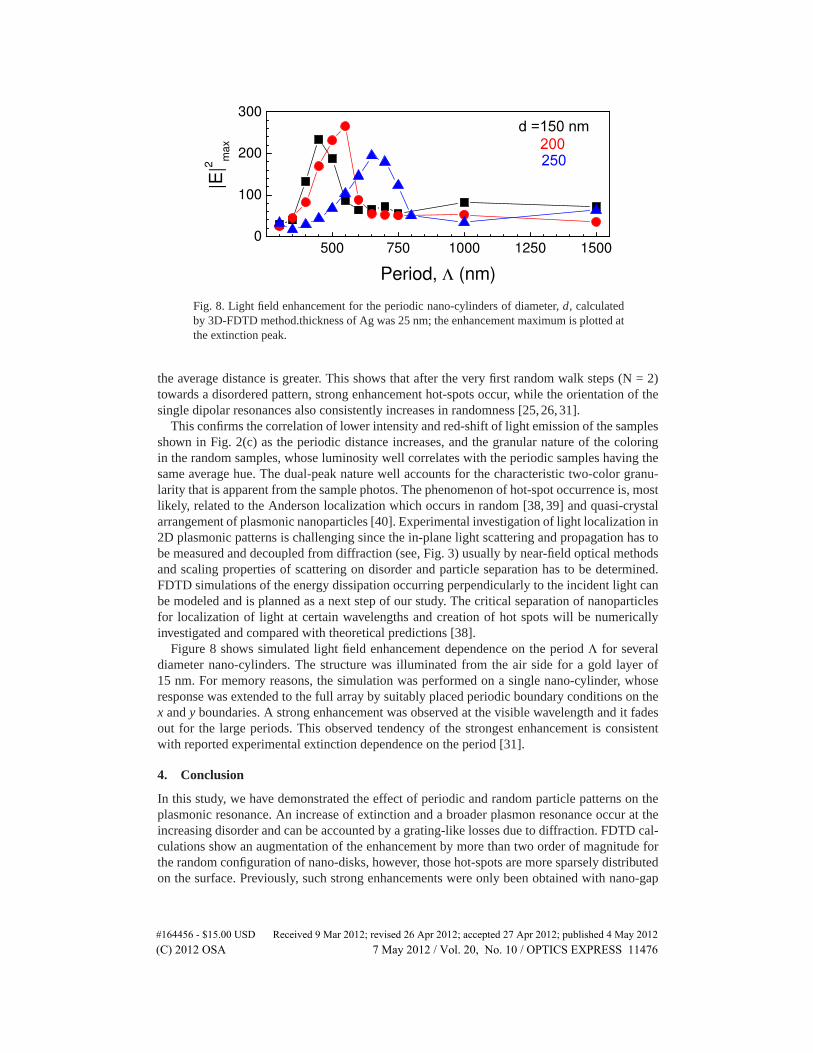
Fig. 8. Light field enhancement for the periodic nano-cylinders of diameter, d, calculatedby 3D-FDTD method.thickness of Ag was 25 nm; the enhancement maximum is plotted atthe extinction peak.
the average distance is greater. This shows that after the very first random walk steps (N = 2)towards a disordered pattern, strong enhancement hot-spots occur, while the orientation of thesingle dipolar resonances also consistently increases in randomness [25, 26, 31].
This confirms the correlation of lower intensity and red-shift of light emission of the samplesshown in Fig. 2(c) as the periodic distance increases, and the granular nature of the coloringin the random samples, whose luminosity well correlates with the periodic samples having thesame average hue. The dual-peak nature well accounts for the characteristic two-color granu-larity that is apparent from the sample photos. The phenomenon of hot-spot occurrence is, mostlikely, related to the Anderson localization which occurs in random [38, 39] and quasi-crystalarrangement of plasmonic nanoparticles [40]. Experimental investigation of light localization in2D plasmonic patterns is challenging since the in-plane light scattering and propagation has tobe measured and decoupled from diffraction (see, Fig. 3) usually by near-field optical methodsand scaling properties of scattering on disorder and particle separation has to be determined.FDTD simulations of the energy dissipation occurring perpendicularly to the incident light canbe modeled and is planned as a next step of our study. The critical separation of nanoparticlesfor localization of light at certain wavelengths and creation of hot spots will be numericallyinvestigated and compared with theoretical predictions [38].
Figure 8 shows simulated light field enhancement dependence on the period Λ for severaldiameter nano-cylinders. The structure was illuminated from the air side for a gold layer of15 nm. For memory reasons, the simulation was performed on a single nano-cylinder, whoseresponse was extended to the full array by suitably placed periodic boundary conditions on thex and y boundaries. A strong enhancement was observed at the visible wavelength and it fadesout for the large periods. This observed tendency of the strongest enhancement is consistentwith reported experimental extinction dependence on the period [31].
4. Conclusion
In this study, we have demonstrated the effect of periodic and random particle patterns on theplasmonic resonance. An increase of extinction and a broader plasmon resonance occur at theincreasing disorder and can be accounted by a grating-like losses due to diffraction. FDTD cal-culations show an augmentation of the enhancement by more than two order of magnitude forthe random configuration of nano-disks, however, those hot-spots are more sparsely distributedon the surface. Previously, such strong enhancements were only been obtained with nano-gap
#164456 - $15.00 USD Received 9 Mar 2012; revised 26 Apr 2012; accepted 27 Apr 2012; published 4 May 2012(C) 2012 OSA 7 May 2012 / Vol. 20, No. 10 / OPTICS EXPRESS 11476

structures (via short-range dipole-dipole interaction) but could not be seen in patterns with largeintra-particle distance.
Theoretical simulation and experimental results shown in this paper should be also applicablenot only to top-down plasmonic technologies, but also to self-assembling patterns. The randomconfiguration is one of the most inexpensive ways to place nano-particles on the substrate,favored for industrials application of LSPR in spectral control of light harvesting for solarcells [12, 41] and sensing [35–37].
Acknowledgments
YN gratefully thanks Prof. Toshihiko Baba of Yokohama National University for fruitful discus-sions and support for facilities, and Prof. Hiroaki Misawa (RIES Hokkaido Univ.) for fruitfuldiscussions; YN has learned the fabrication methods during PhD studies at Hokkaido Univ.This work was financially supported by research grants from Yokohama Academic Foundationand the Research Foundation for Opt-Science and Technology.
#164456 - $15.00 USD Received 9 Mar 2012; revised 26 Apr 2012; accepted 27 Apr 2012; published 4 May 2012(C) 2012 OSA 7 May 2012 / Vol. 20, No. 10 / OPTICS EXPRESS 11477