Surface Mount and Through-Hole Multilayer Ceramic …€¦ · MIL–PRF–49470 was developed as...
25
© KEMET Electronics Corporation • P.O. Box 5928 • Greenville, SC 29606 (864) 963-6300 • www.kemet.com C1031_KPS_SMPS_49470_STACKS • 10/1/2014 1 One world. One KEMET Benefits • -55°C to +125°C operating temperature range • High frequency performance • Bulk capacitance in a reduced footprint • MIL–PRF–49470 QPL • Military Case Codes 3, 4 and 5 • Space Grade available (“T” Level) • DSCC approved (87106) • Commercial/Industrial Grade available • Customer specific requirements available • Low ESR and ESL • High thermal stability • High ripple current capability • Higher reliability than aluminum electrolytic or tantalum • Available encapsulated or unencapsulated Applications • Military • Space • Industrial • Input and output filtering on power supplies – often found on “capacitor banks“ • Snubber circuits • Radar filtering (28 V/microwave burst) Overview KEMET Power Solutions (KPS) MIL Series ceramic stacked capacitors are available in commercial, military and space grades and are well suited for standard and high reliability switch mode power supply (SMPS) and pulse energy applications. Qualified under performance specification MIL–PRF–49470, our military and space grade products meet or exceed the requirements outlined by DSCC (Defense Supply Center, Columbus) and are available in both B (standard reliability) & T (high reliability) product levels. MIL–PRF–49470 was developed as part of a cooperative effort between the U.S. Military, NASA and SMPS suppliers to produce a robust replacement to cancelled DSCC Drawing 87106. The KPS MIL Series is constructed using large chip multilayer ceramic capacitors (MLCCs), horizontally stacked and secured to a lead-frame termination system using a high melting point (HMP) solder alloy. The lead frame isolates the MLCCs from the printed circuit board (PCB) while establishing a parallel circuit configuration. Mechanically isolating the capacitors from the PCB improves mechanical and thermal stress performance, while the parallel circuit configuration allows for bulk capacitance in the same or smaller design footprint. Available in BX, BR, BQ, and X7R dielectrics, these devices are available in encapsulated and unencapsulated styles in both surface mountable and through-hole configurations. Their low Equivalent Series Resistance (ESR) and Equivalent Series Inductance (ESL) make them ideally suited for input and output filtering of power supply as well as snubber applications. The encapsulated styles are primarily used where increased mechanical and environmental protection is required, such as in avionics systems. Surface Mount and Through-Hole Multilayer Ceramic Chip Stacked Capacitors KPS MIL Series, SMPS Stacked Capacitors, MIL–PRF–49470, DSCC 87106, 25 – 1,000 VDC (Commercial, Military, & Space Grades)
Transcript of Surface Mount and Through-Hole Multilayer Ceramic …€¦ · MIL–PRF–49470 was developed as...

© KEMET Electronics Corporation • P.O. Box 5928 • Greenville, SC 29606 (864) 963-6300 • www.kemet.com C1031_KPS_SMPS_49470_STACKS • 10/1/2014 1One world. One KEMET
Benefits
• -55°C to +125°C operating temperature range• High frequency performance• Bulk capacitance in a reduced footprint• MIL–PRF–49470 QPL• Military Case Codes 3, 4 and 5• Space Grade available (“T” Level)• DSCC approved (87106)• Commercial/Industrial Grade available • Customerspecificrequirementsavailable• Low ESR and ESL• High thermal stability• High ripple current capability• Higher reliability than aluminum electrolytic or tantalum• Available encapsulated or unencapsulated
Applications
• Military• Space• Industrial• Inputandoutputfilteringonpowersupplies–oftenfoundon
“capacitor banks“• Snubber circuits• Radarfiltering(28V/microwaveburst)
Overview
KEMET Power Solutions (KPS) MIL Series ceramic stacked capacitors are available in commercial, military and space grades and are well suited for standard and high reliability switch mode powersupply(SMPS)andpulseenergyapplications.QualifiedunderperformancespecificationMIL–PRF–49470,ourmilitaryandspace grade products meet or exceed the requirements outlined by DSCC (Defense Supply Center, Columbus) and are available in both B (standard reliability) & T (high reliability) product levels. MIL–PRF–49470 was developed as part of a cooperative effort between the U.S. Military, NASA and SMPS suppliers to produce a robust replacement to cancelled DSCC Drawing 87106.
The KPS MIL Series is constructed using large chip multilayer ceramic capacitors (MLCCs), horizontally stacked and secured to a lead-frame termination system using a high melting point (HMP) solder alloy. The lead frame isolates the MLCCs from the
printed circuit board (PCB) while establishing a parallel circuit configuration.MechanicallyisolatingthecapacitorsfromthePCBimproves mechanical and thermal stress performance, while the parallelcircuitconfigurationallowsforbulkcapacitanceinthesame or smaller design footprint.
Available in BX, BR, BQ, and X7R dielectrics, these devices are available in encapsulated and unencapsulated styles inbothsurfacemountableandthrough-holeconfigurations.Their low Equivalent Series Resistance (ESR) and Equivalent Series Inductance (ESL) make them ideally suited for input and outputfilteringofpowersupplyaswellassnubberapplications.The encapsulated styles are primarily used where increased mechanical and environmental protection is required, such as in avionics systems.
Surface Mount and Through-Hole Multilayer Ceramic Chip Stacked Capacitors
KPS MIL Series, SMPS Stacked Capacitors, MIL–PRF–49470,DSCC 87106, 25 – 1,000 VDC (Commercial, Military, & Space Grades)

© KEMET Electronics Corporation • P.O. Box 5928 • Greenville, SC 29606 (864) 963-6300 • www.kemet.com C1031_KPS_SMPS_49470_STACKS • 10/1/2014 22
Surface Mount and Through-Hole Multilayer Ceramic Chip Stacked Capacitors – KPS MIL Series, SMPS Stacked Capacitors
MIL–PRF–49470 Ordering Information
M49470 R 01 474 K C NPerformanceSpecification
Indicating MIL–PRF–494701DielectricClassification/
Characteristic2PerformanceSpecificationSheet
Number (Indicating MIL–PRF–49470/1)3Capacitance Code (pF)
Capacitance Tolerance
RatedVoltage(VDC)
Lead Configuration4
M49470 = B level T49470 = T level
A“T”prefixisusedinplace of the “M” for T level product.
Q = BQ R = BRX = BX
01 = Unencapsulated02 = Encapsulated
2SignificantDigits +
Number of Zeros
J = ±5%K = ±10%M = ±20%
A = 50B = 100C = 200E = 500
N = Straight PinL = Formed "L" M= Formed "L" J= Formed "J" K= Formed "J"
1 Indicates performance and reliability requirements. "B" level represents standard reliability."T" level represents high reliability.1 Please refer to performance specification sheet MIL–PRF–49470 for details regarding test levels. The latest revision of the specification sheet is available
through DSCC.1, 3 Test level option "T" is not available on encapsulated stacked devices (i.e. MIL–PRF–49470/2).2 Dielectric classification and characteristic details are outlined in the "Electrical Parameters" section of this document.4 Lead configuration and dimension details are outlined in the "Dimensions" section of this document.
KPS MIL Series, SMPS Stacks Ordering Information(Do not use this ordering code if a QPL MIL–SPEC part type is required. Please order using MIL–SPEC ordering code. Details regarding MIL–PRF–49470 QPL ordering information is outlined above.)
L1 R N 30 C 106 K S 12
Product Family1Dielectric
Classification/Characteristic2
Lead Configuration3
Case Size / Case Code
(CC)
Rated Voltage(VDC)
Capacitance Code (pF)
Capacitance Tolerance Testing Option4 Maximum Height
Dimension (in.)5
L1 = Unencapsulated
L2 = Encapsulated
Q = BQ R = BRX = BXW = X7R
N = StraightL = Formed "L" M= Formed "L" J= Formed "J" K= Formed "J"
30 = CC 340 = CC 450 = CC 5
3 = 255 = 501 = 1002 = 200C = 500B = 630D = 1,000
2SignificantDigits +
Number of Zeros
J = ±5%K = ±10%M = ±20%
B = M49470 "B" LevelT = M49470 "T" LevelC = DSCC87106S = CommercialX = Non-Standard (CustomerSpecificRequirements)
Unencapsulated12 = 0.12"24 = 0.24"36 = 0.36"48 = 0.48"65 = 0.65"
Encapsulated27 = 0.27"39 = 0.39"53 = 0.53"66 = 0.66"80 = 0.80"
1, 4 Test level option "T" is not available on encapsulated stacked devices, i.e., MIL–PRF–49470/2. If a QPL MIL–Spec part type is required, please order using the MIL–Spec ordering code.
2 Dielectric classification and characteristic details are outlined in the "Electrical Parameters" section of this document.3 Lead configuration and dimension details are outlined in the "Dimensions" section of this document. Additional lead configurations may be available. Contact
KEMET for details.4 Indicates performance and reliability requirements. Testing option details are outlined in the "Performance & Reliability" section of this document.4 Please refer to performance specification sheet MIL–PRF–49470 for additional details regarding test levels. The latest revision of the specification sheet is
available through DSCC.4 DSCC Drawing 87106 was cancelled on 01/03/2005. MIL–PRF–49470 capacitors are preferred over DSCC Drawing 87106 capacitors.5 Maximum height dimensions are provided in product tables 1A, 1B, and 1C of this document
Ordering Information Requirements per DSCC Drawing 87106DSCC Drawing 87106 was cancelled on 01/03/2005. Customers can continue to order per 87106 requirements using the original DSCC ordering code,i.e., 87106–001.When available, MIL–PRF–49470 devices are preferred over DSCC Drawing 87106. The MIL–PRF–49470 military specification product provides additional quality assurance provisions that are not required by the DSCC drawing. These extra provisions create a more robust replacement.

© KEMET Electronics Corporation • P.O. Box 5928 • Greenville, SC 29606 (864) 963-6300 • www.kemet.com C1031_KPS_SMPS_49470_STACKS • 10/1/2014 33
Surface Mount and Through-Hole Multilayer Ceramic Chip Stacked Capacitors – KPS MIL Series, SMPS Stacked Capacitors
Construction
Note: Image is exaggerated in order to clearly identify all components of construction
Reference Item MaterialA Leadframe Phosphor Bronze – Alloy 510
B Leadframe Attach Solder Sn10, Pb88, Ag2
C
Termination System1
SnPb (4% minimum)
Solderable SilverD Ni
E Ag
F Electrode PdAg
G Dielectric BaTiO3
H Lead Solder Sn60, Pb40
JEncapsulation2
Molding Compound
K Diallyl-Phthalate (DAP)
1 KEMET reserves the right to construct these devices using either of the termination systems outlined.2 Encapsulated product only, i.e., MIL–PRF–49470/2 and L2 product families.
© KEMET Electronics Corporation • P.O. Box 5928 • Greenville, SC 29606 (864) 963-6300 • www.kemet.com C1031_KPS_SMPS_49470_STACKS • 10/1/2014 44
Surface Mount and Through-Hole Multilayer Ceramic Chip Stacked Capacitors – KPS MIL Series, SMPS Stacked Capacitors
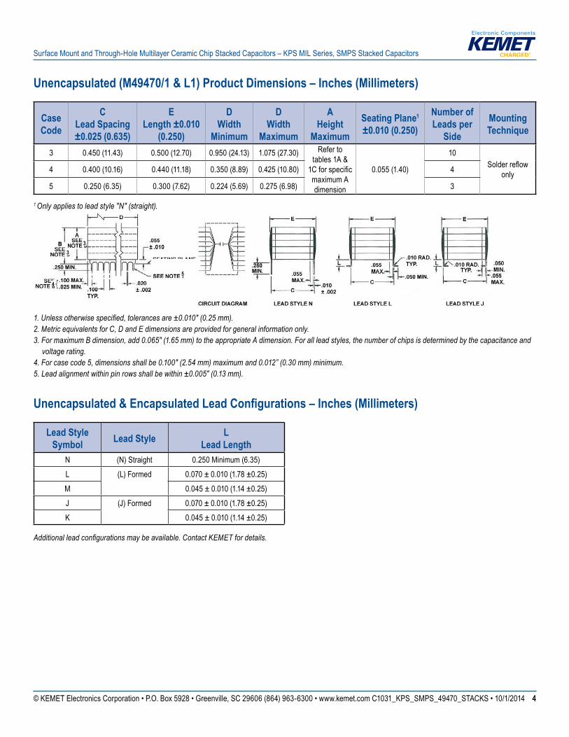
Unencapsulated (M49470/1 & L1) Product Dimensions – Inches (Millimeters)
Case Code
CLead Spacing ±0.025 (0.635)
ELength ±0.010
(0.250)
DWidth
Minimum
DWidth
Maximum
AHeight
Maximum
Seating Plane1 ±0.010 (0.250)
Number of Leads per
Side
Mounting Technique
3 0.450 (11.43) 0.500 (12.70) 0.950 (24.13) 1.075 (27.30) Refer to tables 1A &
1Cforspecificmaximum A dimension
0.055 (1.40)
10 Solderreflow
only4 0.400 (10.16) 0.440 (11.18) 0.350 (8.89) 0.425 (10.80) 4
5 0.250 (6.35) 0.300 (7.62) 0.224 (5.69) 0.275 (6.98) 3
1 Only applies to lead style "N" (straight).
1. Unless otherwise specified, tolerances are ±0.010" (0.25 mm).2. Metric equivalents for C, D and E dimensions are provided for general information only.3. For maximum B dimension, add 0.065" (1.65 mm) to the appropriate A dimension. For all lead styles, the number of chips is determined by the capacitance and
voltage rating.4. For case code 5, dimensions shall be 0.100" (2.54 mm) maximum and 0.012” (0.30 mm) minimum.5. Lead alignment within pin rows shall be within ±0.005" (0.13 mm).
Unencapsulated & Encapsulated Lead Configurations – Inches (Millimeters)
Lead Style Symbol Lead Style L
Lead LengthN (N) Straight 0.250 Minimum (6.35)L (L) Formed 0.070 ± 0.010 (1.78 ±0.25)M 0.045 ± 0.010 (1.14 ±0.25)J (J) Formed 0.070 ± 0.010 (1.78 ±0.25)K 0.045 ± 0.010 (1.14 ±0.25)
Additional lead configurations may be available. Contact KEMET for details.
33
4
5

© KEMET Electronics Corporation • P.O. Box 5928 • Greenville, SC 29606 (864) 963-6300 • www.kemet.com C1031_KPS_SMPS_49470_STACKS • 10/1/2014 55
Surface Mount and Through-Hole Multilayer Ceramic Chip Stacked Capacitors – KPS MIL Series, SMPS Stacked Capacitors
Encapsulated (M49470/2 & L2) Product Dimensions – Inches (Millimeters)
Case CodeC
Lead Spacing ±0.025 (0.635)
ELength
Maximum
DWidth ±0.635
(±0.025)
AHeight
Number of Leads per Side
Mounting Technique
3 0.450 (11.43) 0.580 (14.73) 1.155 (29.34) Refer to table 1B for specificmaximumA
dimension
10 Solderreflowonly
4 0.400 (10.16) 0.485 (12.32) 0.485 (12.32) 4
5 0.250 (6.35) 0.355 (9.02) 0.355 (9.02) 3
1. Dimensions are in inches.2. Metric equivalents are given for general information only.3. Unless otherwise specified, tolerances are ±0.010” (0.25 mm).4. Lead alignment within pin rows shall be within ±0.005” (0.13 mm).
Unencapsulated & Encapsulated Lead Configurations – Inches (Millimeters)
Lead Style Symbol Lead Style L
Lead LengthN (N) Straight 0.250 Minimum (6.35)L (L) Formed 0.070 ± 0.010 (1.78 ±0.25)M 0.045 ± 0.010 (1.14 ±0.25)J (J) Formed 0.070 ± 0.010 (1.78 ±0.25)K 0.045 ± 0.010 (1.14 ±0.25)
Additional lead configurations may be available. Contact KEMET for details.
SEE NOTE 4
© KEMET Electronics Corporation • P.O. Box 5928 • Greenville, SC 29606 (864) 963-6300 • www.kemet.com C1031_KPS_SMPS_49470_STACKS • 10/1/2014 66
Surface Mount and Through-Hole Multilayer Ceramic Chip Stacked Capacitors – KPS MIL Series, SMPS Stacked Capacitors
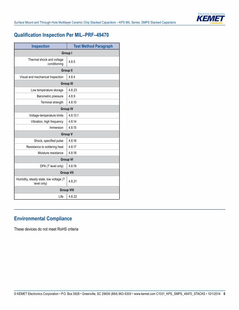
Qualification Inspection Per MIL–PRF–49470
Inspection Test Method Paragraph Group I
Thermal shock and voltage conditioning 4.8.5
Group II
VisualandmechanicalInspection 4.8.4
Group III
Low temperature storage 4.8.23Barometric pressure 4.8.9
Terminal strength 4.8.10
Group IV
Voltage-temperaturelimits 4.8.13.1Vibration,highfrequency 4.8.14
Immersion 4.8.15
Group V
Shock,specifiedpulse 4.8.16Resistance to soldering heat 4.8.17
Moisture resistance 4.8.18
Group VI
DPA (T level only) 4.8.19
Group VII
Humidity, steady state, low voltage (T level only) 4.8.21
Group VIII
Life 4.8.22
Environmental Compliance
These devices do not meet RoHS criteria

© KEMET Electronics Corporation • P.O. Box 5928 • Greenville, SC 29606 (864) 963-6300 • www.kemet.com C1031_KPS_SMPS_49470_STACKS • 10/1/2014 77
Surface Mount and Through-Hole Multilayer Ceramic Chip Stacked Capacitors – KPS MIL Series, SMPS Stacked Capacitors
Electrical Parameters/Performance Characteristics: BQ Dielectric
Item Parameters/CharacteristicsOperating Temperature Range -55°C to +125°C
CapacitanceChangewithReferenceto+25°Cand0VDCApplied(TCC) ±15%
CapacitanceChangewithReferenceto+25°Cand100%RatedVDCApplied +15%, -50%
Aging Rate (Maximum % Capacitance Loss/Decade Hour) 1%
DielectricWithstandingVoltage(DWV)250%ofratedDCvoltageforvoltagerating<500V 150%ofratedDCvoltageforvoltageratingof500V (5 ±1 seconds and charge/discharge not exceeding 50 mA)
Dissipation Factor (DF) Maximum Limit @ 25ºC 2.5%
Insulation Resistance (IR) Limit @ 25°C 1,000megohmmicrofarads(minimum)or100GΩ
Insulation Resistance (IR) Limit @ 125°C 100megohmmicrofarads(minimum)or10GΩ
Regarding aging rate: Capacitance measurements (including tolerance) are indexed to a referee time of 1,000 hours.To obtain IR limit, divide MΩ-µF value by the capacitance and compare to GΩ limit. Select the lower of the two limits.Capacitance and dissipation factor (DF) measured under the following conditions: 1 kHz ±100 Hz at 1.0 Vrms ±0.2 Vrms (open circuit voltage).Note: When measuring capacitance it is important to ensure the set voltage level is held constant. The HP4284 and Agilent E4980 have a feature known as Automatic Level Control (ALC). The ALC feature should be switched to "ON."
Electrical Parameters/Performance Characteristics: BR Dielectric
Item Parameters/CharacteristicsOperating Temperature Range -55°C to +125°C
CapacitanceChangewithReferenceto+25°Cand0VDCApplied(TCC) ±15%
CapacitanceChangewithReferenceto+25°Cand100%RatedVDCApplied +15%, -40%
Aging Rate (Maximum % Capacitance Loss/Decade Hour) 1%
DielectricWithstandingVoltage(DWV)250%ofratedDCvoltageforvoltagerating<500V 150%ofratedDCvoltageforvoltageratingof500V (5 ±1 seconds and charge/discharge not exceeding 50 mA)
Dissipation Factor (DF) Maximum Limit @ 25ºC 2.5%
Insulation Resistance (IR) Limit @ 25°C 1,000megohmmicrofarads(minimum)or100GΩ
Insulation Resistance (IR) Limit @ 125°C 100megohmmicrofarads(minimum)or10GΩ
Regarding aging rate: Capacitance measurements (including tolerance) are indexed to a referee time of 1,000 hours. To obtain IR limit, divide MΩ-µF value by the capacitance and compare to GΩ limit. Select the lower of the two limits. Capacitance and dissipation factor (DF) measured under the following conditions: 1 kHz ±100 Hz at 1.0 Vrms ±0.2 Vrms (open circuit voltage).Note: When measuring capacitance it is important to ensure the set voltage level is held constant. The HP4284 and Agilent E4980 have a feature known as Automatic Level Control (ALC). The ALC feature should be switched to "ON."

© KEMET Electronics Corporation • P.O. Box 5928 • Greenville, SC 29606 (864) 963-6300 • www.kemet.com C1031_KPS_SMPS_49470_STACKS • 10/1/2014 88
Surface Mount and Through-Hole Multilayer Ceramic Chip Stacked Capacitors – KPS MIL Series, SMPS Stacked Capacitors
Electrical Parameters/Performance Characteristics: BX Dielectric
Item Parameters/CharacteristicsOperating Temperature Range -55°C to +125°C
CapacitanceChangewithReferenceto+25°Cand0VDCApplied(TCC) ±15%
CapacitanceChangewithReferenceto+25°Cand100%RatedVDCApplied +15%, -25%
Aging Rate (Maximum % Capacitance Loss/Decade Hour) 1%
DielectricWithstandingVoltage(DWV)250%ofratedDCvoltageforvoltagerating<500V 150%ofratedDCvoltageforvoltageratingof500V (5 ±1 seconds and charge/discharge not exceeding 50 mA)
Dissipation Factor (DF) Maximum Limit @ 25ºC 2.5%
Insulation Resistance (IR) Limit @ 25°C 1000megohmmicrofarads(minimum)or100GΩ
Insulation Resistance (IR) Limit @ 125°C 100megohmmicrofarads(minimum)or10GΩ
Regarding aging rate: Capacitance measurements (including tolerance) are indexed to a referee time of 1000 hours. To obtain IR limit, divide MΩ-µF value by the capacitance and compare to GΩ limit. Select the lower of the two limits. Capacitance and dissipation factor (DF) measured under the following conditions: 1 kHz ±100 Hz at 1.0 Vrms ±0.2 Vrms (open circuit voltage).Note: When measuring capacitance it is important to ensure the set voltage level is held constant. The HP4284 and Agilent E4980 have a feature known as Automatic Level Control (ALC). The ALC feature should be switched to "ON."
Electrical Parameters/Performance Characteristics: X7R Dielectric
Item Parameters/CharacteristicsOperating Temperature Range -55°C to +125°C
CapacitanceChangewithReferenceto+25°Cand0VDCApplied(TCC) ±15%
Aging Rate (Maximum % Capacitance Loss/Decade Hour) 3.0%
DielectricWithstandingVoltage(DWV) 250% of rated voltage (5 ±1 seconds and charge/discharge not exceeding 50 mA)
Dissipation Factor (DF) Maximum Limit @ 25ºC 3.5%(25V)and2.5%(50Vto200V)
Insulation Resistance (IR) Limit @ 25°C 1,000megohmmicrofaradsor100GΩ (Rated voltage applied for 120 ±5 seconds @ 25°C)
Regarding aging rate: Capacitance measurements (including tolerance) are indexed to a referee time of 1000 hours.To obtain IR limit, divide MΩ-µF value by the capacitance and compare to GΩ limit. Select the lower of the two limits.Capacitance and dissipation factor (DF) measured under the following conditions: 1 kHz ±50 Hz and 1.0 ±0.2 Vrms if capacitance ≤ 10 µF. 20 Hz ±10 Hz and 0.5 ±0.1 Vrms if capacitance > 10 µF.Note: When measuring capacitance it is important to ensure the set voltage level is held constant. The HP4284 and Agilent E4980 have a feature known as Automatic Level Control (ALC). The ALC feature should be switched to "ON."

© KEMET Electronics Corporation • P.O. Box 5928 • Greenville, SC 29606 (864) 963-6300 • www.kemet.com C1031_KPS_SMPS_49470_STACKS • 10/1/2014 99
Surface Mount and Through-Hole Multilayer Ceramic Chip Stacked Capacitors – KPS MIL Series, SMPS Stacked Capacitors
MIL–PRF–49470/1 Unencapsulated, Horizontally Stacked
MIL–PRF–49470 P/N 1 Capacitance (µF)
Case Code
Height A inch (mm)
Capacitance Tolerance
Lead Configuration KEMET P/N 1
50 VDC – BX Dielectric (1)49470X01105(2)A(3) 1 5 0.120 (3.05) K, M N, L, M, J, K L1X(3)505105(2)(4)12(1)49470X01125(2)A(3) 1.2 5 0.120 (3.05) K, M N, L, M, J, K L1X(3)505125(2)(4)12(1)49470X01155(2)A(3) 1.5 5 0.240 (6.10) K, M N, L, M, J, K L1X(3)505155(2)(4)24(1)49470X01185(2)A(3) 1.8 5 0.240 (6.10) K, M N, L, M, J, K L1X(3)505185(2)(4)24(1)49470X01225(2)A(3) 2.2 5 0.240 (6.10) K, M N, L, M, J, K L1X(3)505225(2)(4)24(1)49470X01275(2)A(3) 2.7 5 0.360 (9.14) K, M N, L, M, J, K L1X(3)505275(2)(4)36(1)49470X01335(2)A(3) 3.3 5 0.360 (9.14) K, M N, L, M, J, K L1X(3)505335(2)(4)36(1)49470X01475(2)A(3) 3.9 5 0.480 (12.19) K, M N, L, M, J, K L1X(3)505475(2)(4)48(1)49470X01395(2)A(3) 3.9 5 0.480 (12.19) K, M N, L, M, J, K L1X(3)505395(2)(4)48(1)49470X01565(2)A(3) 5.6 5 0.650 (16.51) K, M N, L, M, J, K L1X(3)505565(2)(4)65(1)49470X01685(2)A(3) 6.8 4 0.360 (9.14) K, M N, L, M, J, K L1X(3)405685(2)(4)36(1)49470X01825(2)A(3) 8.2 4 0.360 (9.14) K, M N, L, M, J, K L1X(3)405825(2)(4)36(1)49470X01106(2)A(3) 10 4 0.480 (12.19) K, M N, L, M, J, K L1X(3)405106(2)(4)48(1)49470X01126(2)A(3) 12 4 0.480 (12.19) K, M N, L, M, J, K L1X(3)405126(2)(4)48(1)49470X01156(2)A(3) 15 4 0.650 (16.51) K, M N, L, M, J, K L1X(3)405156(2)(4)65(1)49470X01186(2)A(3) 18 3 0.240 (6.10) K, M N, L, M, J, K L1X(3)305186(2)(4)24(1)49470X01226(2)A(3) 22 3 0.360 (9.14) K, M N, L, M, J, K L1X(3)305226(2)(4)36(1)49470X01276(2)A(3) 27 3 0.360 (9.14) K, M N, L, M, J, K L1X(3)305276(2)(4)36(1)49470X01336(2)A(3) 33 3 0.360 (9.14) K, M N, L, M, J, K L1X(3)305336(2)(4)36(1)49470X01396(2)A(3) 39 3 0.480 (12.19) K, M N, L, M, J, K L1X(3)305396(2)(4)48(1)49470X01476(2)A(3) 47 3 0.650 (16.51) K, M N, L, M, J, K L1X(3)305476(2)(4)65
100 VDC – BX Dielectric (1)49470X01684(2)B(3) 0.68 5 0.120 (3.05) K, M N, L, M, J, K L1X(3)501684(2)(4)12(1)49470X01824(2)B(3) 0.82 5 0.240 (6.10) K, M N, L, M, J, K L1X(3)501824(2)(4)24(1)49470X01105(2)B(3) 1 5 0.240 (6.10) K, M N, L, M, J, K L1X(3)501105(2)(4)24(1)49470X01125(2)B(3) 1.2 5 0.240 (6.10) K, M N, L, M, J, K L1X(3)501125(2)(4)24(1)49470X01155(2)B(3) 1.5 5 0.360 (9.14) K, M N, L, M, J, K L1X(3)501155(2)(4)36(1)49470X01185(2)B(3) 1.8 5 0.360 (9.14) K, M N, L, M, J, K L1X(3)501185(2)(4)36(1)49470X01225(2)B(3) 2.2 5 0.480 (12.19) K, M N, L, M, J, K L1X(3)501225(2)(4)48(1)49470X01275(2)B(3) 2.7 5 0.480 (12.19) K, M N, L, M, J, K L1X(3)501275(2)(4)48(1)49470X01335(2)B(3) 3.3 5 0.650 (16.51) K, M N, L, M, J, K L1X(3)501335(2)(4)65(1)49470X01395(2)B(3) 3.9 4 0.360 (9.14) K, M N, L, M, J, K L1X(3)401395(2)(4)36(1)49470X01475(2)B(3) 4.7 4 0.360 (9.14) K, M N, L, M, J, K L1X(3)401475(2)(4)36(1)49470X01565(2)B(3) 5.6 4 0.480 (12.19) K, M N, L, M, J, K L1X(3)401565(2)(4)48(1)49470X01685(2)B(3) 6.8 4 0.480 (12.19) K, M N, L, M, J, K L1X(3)401685(2)(4)48(1)49470X01825(2)B(3) 8.2 4 0.650 (16.51) K, M N, L, M, J, K L1X(3)401825(2)(4)65(1)49470X01106(2)B(3) 10 3 0.240 (6.10) K, M N, L, M, J, K L1X(3)301106(2)(4)24(1)49470X01126(2)B(3) 12 3 0.240 (6.10) K, M N, L, M, J, K L1X(3)301126(2)(4)24(1)49470X01156(2)B(3) 15 3 0.360 (9.14) K, M N, L, M, J, K L1X(3)301156(2)(4)36(1)49470X01186(2)B(3) 18 3 0.360 (9.14) K, M N, L, M, J, K L1X(3)301186(2)(4)36(1)49470X01226(2)B(3) 22 3 0.480 (12.19) K, M N, L, M, J, K L1X(3)301226(2)(4)48(1)49470X01276(2)B(3) 27 3 0.650 (16.51) K, M N, L, M, J, K L1X(3)301276(2)(4)65
200 VDC – BR Dielectric (1)49470R01474(2)C(3) 0.47 5 0.240 (6.10) K, M N, L, M, J, K L1R(3)502474(2)(4)24(1)49470R01564(2)C(3) 0.56 5 0.240 (6.10) K, M N, L, M, J, K L1R(3)502564(2)(4)24(1)49470R01684(2)C(3) 0.68 5 0.360 (9.14) K, M N, L, M, J, K L1R(3)502684(2)(4)36(1)49470R01824(2)C(3) 0.82 5 0.360 (9.14) K, M N, L, M, J, K L1R(3)502824(2)(4)36(1)49470R01105(2)C(3) 1 5 0.480 (12.19) K, M N, L, M, J, K L1R(3)502105(2)(4)48
MIL–PRF–49470 P/N 1 Capacitance (µF) Case Code Height A inch (mm)
Capacitance Tolerance Lead Configuration KEMET P/N 1
Table 1A – MIL–PRF–49470/1, Product Selection 50 – 200 VDC
1 Complete P/N requires additional characters in the numbered positions provided in order to indicate product level (B level or T level), capacitance tolerance and lead configuration. For each numbered position, available options are as follows: (1) Test level character "M" for B level, or "T" for T level (MIL–PRF–49470/1 part number only). (2) Capacitance tolerance character " K" or " M". (3) Lead style character " N", "L", "M", "J" or "K". (4) Test level character "B" for B level, or "T" for T level (KEMET part number only).

© KEMET Electronics Corporation • P.O. Box 5928 • Greenville, SC 29606 (864) 963-6300 • www.kemet.com C1031_KPS_SMPS_49470_STACKS • 10/1/2014 1010
Surface Mount and Through-Hole Multilayer Ceramic Chip Stacked Capacitors – KPS MIL Series, SMPS Stacked Capacitors
MIL–PRF–49470/1 Unencapsulated, Horizontally Stacked
MIL–PRF–49470 P/N 1 Capacitance (µF)
Case Code
Height A inch (mm)
Capacitance Tolerance
Lead Configuration KEMET P/N 1
(1)49470R01125(2)C(3) 1.2 5 0.480 (12.19) K, M N, L, M, J, K L1R(3)502125(2)(4)48(1)49470R01155(2)C(3) 1.5 5 0.650 (16.51) K, M N, L, M, J, K L1R(3)502155(2)(4)65(1)49470R01185(2)C(3) 1.8 4 0.360 (9.14) K, M N, L, M, J, K L1R(3)402185(2)(4)36(1)49470R01225(2)C(3) 2.2 4 0.360 (9.14) K, M N, L, M, J, K L1R(3)402225(2)(4)36(1)49470R01275(2)C(3) 2.7 4 0.480 (12.19) K, M N, L, M, J, K L1R(3)402275(2)(4)48(1)49470R01335(2)C(3) 3.3 4 0.480 (12.19) K, M N, L, M, J, K L1R(3)402335(2)(4)48(1)49470R01395(2)C(3) 3.9 4 0.650 (16.51) K, M N, L, M, J, K L1R(3)402395(2)(4)65(1)49470R01475(2)C(3) 4.7 3 0.240 (6.10) K, M N, L, M, J, K L1R(3)302475(2)(4)24(1)49470R01565(2)C(3) 5.6 3 0.240 (6.10) K, M N, L, M, J, K L1R(3)302565(2)(4)24(1)49470R01685(2)C(3) 6.8 3 0.360 (9.14) K, M N, L, M, J, K L1R(3)302685(2)(4)36(1)49470R01825(2)C(3) 8.2 3 0.360 (9.14) K, M N, L, M, J, K L1R(3)302825(2)(4)36(1)49470R01106(2)C(3) 10 3 0.480 (12.19) K, M N, L, M, J, K L1R(3)302106(2)(4)48(1)49470R01126(2)C(3) 12 3 0.650 (16.51) K, M N, L, M, J, K L1R(3)302126(2)(4)65
500 VDC – BQ Dielectric (1)49470Q01154(2)E(3) 0.15 5 0.120 (3.05) K, M N, L, M, J, K L1Q(3)50C154(2)(4)12(1)49470Q01184(2)E(3) 0.18 5 0.240 (6.10) K, M N, L, M, J, K L1Q(3)50C184(2)(4)24(1)49470Q01224(2)E(3) 0.22 5 0.240 (6.10) K, M N, L, M, J, K L1Q(3)50C224(2)(4)24(1)49470Q01274(2)E(3) 0.27 5 0.240 (6.10) K, M N, L, M, J, K L1Q(3)50C274(2)(4)24(1)49470Q01334(2)E(3) 0.33 5 0.360 (9.14) K, M N, L, M, J, K L1Q(3)50C334(2)(4)36(1)49470Q01394(2)E(3) 0.39 5 0.360 (9.14) K, M N, L, M, J, K L1Q(3)50C394(2)(4)36(1)49470Q01474(2)E(3) 0.47 5 0.360 (9.14) K, M N, L, M, J, K L1Q(3)50C474(2)(4)36(1)49470Q01564(2)E(3) 0.56 5 0.480 (12.19) K, M N, L, M, J, K L1Q(3)50C564(2)(4)48(1)49470Q01684(2)E(3) 0.68 5 0.650 (16.51) K, M N, L, M, J, K L1Q(3)50C684(2)(4)65(1)49470Q01824(2)E(3) 0.82 4 0.360 (9.14) K, M N, L, M, J, K L1Q(3)40C824(2)(4)36(1)49470Q01105(2)E(3) 1 4 0.360 (9.14) K, M N, L, M, J, K L1Q(3)40C105(2)(4)36(1)49470Q01125(2)E(3) 1.2 4 0.360 (9.14) K, M N, L, M, J, K L1Q(3)40C125(2)(4)36(1)49470Q01155(2)E(3) 1.5 4 0.480 (12.19) K, M N, L, M, J, K L1Q(3)40C155(2)(4)48(1)49470Q01185(2)E(3) 1.8 4 0.650 (16.51) K, M N, L, M, J, K L1Q(3)40C185(2)(4)65(1)49470Q01225(2)E(3) 2.2 3 0.240 (6.10) K, M N, L, M, J, K L1Q(3)30C225(2)(4)24(1)49470Q01275(2)E(3) 2.7 3 0.360 (9.14) K, M N, L, M, J, K L1Q(3)30C275(2)(4)36(1)49470Q01335(2)E(3) 3.3 3 0.360 (9.14) K, M N, L, M, J, K L1Q(3)30C335(2)(4)36(1)49470Q01395(2)E(3) 3.9 3 0.360 (9.14) K, M N, L, M, J, K L1Q(3)30C395(2)(4)36(1)49470Q01475(2)E(3) 4.7 3 0.480 (12.19) K, M N, L, M, J, K L1Q(3)30C475(2)(4)48(1)49470Q01565(2)E(3) 5.6 3 0.650 (16.51) K, M N, L, M, J, K L1Q(3)30C565(2)(4)65
MIL–PRF–49470 P/N 1 Capacitance (µF) Case Code Height A inch (mm)
Capacitance Tolerance Lead Configuration KEMET P/N 1
Table 1A – MIL–PRF–49470 /1, Product Selection 200 – 500 VDC cont'd
1 Complete P/N requires additional characters in the numbered positions provided in order to indicate product level (B level or T level), capacitance tolerance and lead configuration. For each numbered position, available options are as follows: (1) Test level character "M" for B level, or "T" for T level (MIL-PRF-49470/1 part number only). (2) Capacitance tolerance character " K" or " M". (3) Lead style character " N", "L", "M", "J" or "K". (4) Test level character "B" for B level, or "T" for T level (KEMET part number only).
© KEMET Electronics Corporation • P.O. Box 5928 • Greenville, SC 29606 (864) 963-6300 • www.kemet.com C1031_KPS_SMPS_49470_STACKS • 10/1/2014 1111
Surface Mount and Through-Hole Multilayer Ceramic Chip Stacked Capacitors – KPS MIL Series, SMPS Stacked Capacitors
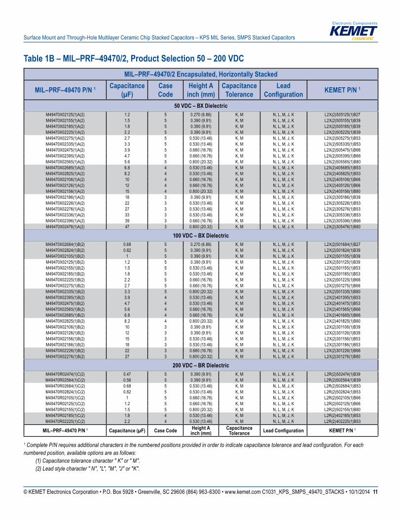
MIL–PRF–49470/2 Encapsulated, Horizontally Stacked
MIL–PRF–49470 P/N 1 Capacitance (µF)
Case Code
Height A inch (mm)
Capacitance Tolerance
Lead Configuration KEMET P/N 1
50 VDC – BX Dielectric M49470X02125(1)A(2) 1.2 5 0.270 (6.86) K, M N, L, M, J, K L2X(2)505125(1)B27M49470X02155(1)A(2) 1.5 5 0.390 (9.91) K, M N, L, M, J, K L2X(2)505155(1)B39M49470X02185(1)A(2) 1.8 5 0.390 (9.91) K, M N, L, M, J, K L2X(2)505185(1)B39M49470X02225(1)A(2) 2.2 5 0.390 (9.91) K, M N, L, M, J, K L2X(2)505225(1)B39M49470X02275(1)A(2) 2.7 5 0.530 (13.46) K, M N, L, M, J, K L2X(2)505275(1)B53M49470X02335(1)A(2) 3.3 5 0.530 (13.46) K, M N, L, M, J, K L2X(2)505335(1)B53M49470X02475(1)A(2) 3.9 5 0.660 (16.76) K, M N, L, M, J, K L2X(2)505475(1)B66M49470X02395(1)A(2) 4.7 5 0.660 (16.76) K, M N, L, M, J, K L2X(2)505395(1)B66M49470X02565(1)A(2) 5.6 5 0.800 (20.32) K, M N, L, M, J, K L2X(2)505565(1)B80M49470X02685(1)A(2) 6.8 4 0.530 (13.46) K, M N, L, M, J, K L2X(2)405685(1)B53M49470X02825(1)A(2) 8.2 4 0.530 (13.46) K, M N, L, M, J, K L2X(2)405825(1)B53M49470X02106(1)A(2) 10 4 0.660 (16.76) K, M N, L, M, J, K L2X(2)405106(1)B66M49470X02126(1)A(2) 12 4 0.660 (16.76) K, M N, L, M, J, K L2X(2)405126(1)B66M49470X02156(1)A(2) 15 4 0.800 (20.32) K, M N, L, M, J, K L2X(2)405156(1)B80M49470X02186(1)A(2) 18 3 0.390 (9.91) K, M N, L, M, J, K L2X(2)305186(1)B39M49470X02226(1)A(2) 22 3 0.530 (13.46) K, M N, L, M, J, K L2X(2)305226(1)B53M49470X02276(1)A(2) 27 3 0.530 (13.46) K, M N, L, M, J, K L2X(2)305276(1)B53M49470X02336(1)A(2) 33 3 0.530 (13.46) K, M N, L, M, J, K L2X(2)305336(1)B53M49470X02396(1)A(2) 39 3 0.660 (16.76) K, M N, L, M, J, K L2X(2)305396(1)B66M49470X02476(1)A(2) 47 3 0.800 (20.32) K, M N, L, M, J, K L2X(2)305476(1)B80
100 VDC – BX Dielectric M49470X02684(1)B(2) 0.68 5 0.270 (6.86) K, M N, L, M, J, K L2X(2)501684(1)B27M49470X02824(1)B(2) 0.82 5 0.390 (9.91) K, M N, L, M, J, K L2X(2)501824(1)B39M49470X02105(1)B(2) 1 5 0.390 (9.91) K, M N, L, M, J, K L2X(2)501105(1)B39M49470X02125(1)B(2) 1.2 5 0.390 (9.91) K, M N, L, M, J, K L2X(2)501125(1)B39M49470X02155(1)B(2) 1.5 5 0.530 (13.46) K, M N, L, M, J, K L2X(2)501155(1)B53M49470X02185(1)B(2) 1.8 5 0.530 (13.46) K, M N, L, M, J, K L2X(2)501185(1)B53M49470X02225(1)B(2) 2.2 5 0.660 (16.76) K, M N, L, M, J, K L2X(2)501225(1)B66M49470X02275(1)B(2) 2.7 5 0.660 (16.76) K, M N, L, M, J, K L2X(2)501275(1)B66M49470X02335(1)B(2) 3.3 5 0.800 (20.32) K, M N, L, M, J, K L2X(2)501335(1)B80M49470X02395(1)B(2) 3.9 4 0.530 (13.46) K, M N, L, M, J, K L2X(2)401395(1)B53M49470X02475(1)B(2) 4.7 4 0.530 (13.46) K, M N, L, M, J, K L2X(2)401475(1)B53M49470X02565(1)B(2) 5.6 4 0.660 (16.76) K, M N, L, M, J, K L2X(2)401565(1)B66M49470X02685(1)B(2) 6.8 4 0.660 (16.76) K, M N, L, M, J, K L2X(2)401685(1)B66M49470X02825(1)B(2) 8.2 4 0.800 (20.32) K, M N, L, M, J, K L2X(2)401825(1)B80M49470X02106(1)B(2) 10 3 0.390 (9.91) K, M N, L, M, J, K L2X(2)301106(1)B39M49470X02126(1)B(2) 12 3 0.390 (9.91) K, M N, L, M, J, K L2X(2)301126(1)B39M49470X02156(1)B(2) 15 3 0.530 (13.46) K, M N, L, M, J, K L2X(2)301156(1)B53M49470X02186(1)B(2) 18 3 0.530 (13.46) K, M N, L, M, J, K L2X(2)301186(1)B53M49470X02226(1)B(2) 22 3 0.660 (16.76) K, M N, L, M, J, K L2X(2)301226(1)B66M49470X02276(1)B(2) 27 3 0.800 (20.32) K, M N, L, M, J, K L2X(2)301276(1)B80
200 VDC – BR Dielectric M49470R02474(1)C(2) 0.47 5 0.390 (9.91) K, M N, L, M, J, K L2R(2)502474(1)B39M49470R02564(1)C(2) 0.56 5 0.390 (9.91) K, M N, L, M, J, K L2R(2)502564(1)B39M49470R02684(1)C(2) 0.68 5 0.530 (13.46) K, M N, L, M, J, K L2R(2)502684(1)B53M49470R02824(1)C(2) 0.82 5 0.530 (13.46) K, M N, L, M, J, K L2R(2)502824(1)B53M49470R02105(1)C(2) 1 5 0.660 (16.76) K, M N, L, M, J, K L2R(2)502105(1)B66M49470R02125(1)C(2) 1.2 5 0.660 (16.76) K, M N, L, M, J, K L2R(2)502125(1)B66M49470R02155(1)C(2) 1.5 5 0.800 (20.32) K, M N, L, M, J, K L2R(2)502155(1)B80M49470R02185(1)C(2) 1.8 4 0.530 (13.46) K, M N, L, M, J, K L2R(2)402185(1)B53M49470R02225(1)C(2) 2.2 4 0.530 (13.46) K, M N, L, M, J, K L2R(2)402225(1)B53
MIL–PRF–49470 P/N 1 Capacitance (µF) Case Code Height A inch (mm)
Capacitance Tolerance Lead Configuration KEMET P/N 1
Table 1B – MIL–PRF–49470/2, Product Selection 50 – 200 VDC
1 Complete P/N requires additional characters in the numbered positions provided in order to indicate capacitance tolerance and lead configuration. For each numbered position, available options are as follows: (1) Capacitance tolerance character " K" or " M". (2) Lead style character " N", "L", "M", "J" or "K".

© KEMET Electronics Corporation • P.O. Box 5928 • Greenville, SC 29606 (864) 963-6300 • www.kemet.com C1031_KPS_SMPS_49470_STACKS • 10/1/2014 1212
Surface Mount and Through-Hole Multilayer Ceramic Chip Stacked Capacitors – KPS MIL Series, SMPS Stacked Capacitors
MIL–PRF–49470/2 Encapsulated, Horizontally Stacked
MIL–PRF–49470 P/N 1 Capacitance (µF)
Case Code
Height A inch (mm)
Capacitance Tolerance
Lead Configuration KEMET P/N 1
M49470R02275(1)C(2) 2.7 4 0.660 (16.76) K, M N, L, M, J, K L2R(2)402275(1)B66M49470R02335(1)C(2) 3.3 4 0.660 (16.76) K, M N, L, M, J, K L2R(2)402335(1)B66M49470R02395(1)C(2) 3.9 4 0.800 (20.32) K, M N, L, M, J, K L2R(2)402395(1)B80M49470R02475(1)C(2) 4.7 3 0.390 (9.91) K, M N, L, M, J, K L2R(2)302475(1)B39M49470R02565(1)C(2) 5.6 3 0.390 (9.91) K, M N, L, M, J, K L2R(2)302565(1)B39M49470R02685(1)C(2) 6.8 3 0.530 (13.46) K, M N, L, M, J, K L2R(2)302685(1)B53M49470R02825(1)C(2) 8.2 3 0.530 (13.46) K, M N, L, M, J, K L2R(2)302825(1)B53M49470R02106(1)C(2) 10 3 0.660 (16.76) K, M N, L, M, J, K L2R(2)302106(1)B66M49470R02126(1)C(2) 12 3 0.800 (20.32) K, M N, L, M, J, K L2R(2)302126(1)B80
500 VDC – BQ Dielectric M49470Q02154(1)E(2) 0.15 5 0.270 (6.86) K, M N, L, M, J, K L2Q(2)50C154(1)B27M49470Q02184(1)E(2) 0.18 5 0.390 (9.91) K, M N, L, M, J, K L2Q(2)50C184(1)B39M49470Q02224(1)E(2) 0.22 5 0.390 (9.91) K, M N, L, M, J, K L2Q(2)50C224(1)B39M49470Q02274(1)E(2) 0.27 5 0.390 (9.91) K, M N, L, M, J, K L2Q(2)50C274(1)B39M49470Q02334(1)E(2) 0.33 5 0.530 (13.46) K, M N, L, M, J, K L2Q(2)50C334(1)B53M49470Q02394(1)E(2) 0.39 5 0.530 (13.46) K, M N, L, M, J, K L2Q(2)50C394(1)B53M49470Q02474(1)E(2) 0.47 5 0.530 (13.46) K, M N, L, M, J, K L2Q(2)50C474(1)B53M49470Q02564(1)E(2) 0.56 5 0.660 (16.76) K, M N, L, M, J, K L2Q(2)50C564(1)B66M49470Q02684(1)E(2) 0.68 5 0.800 (20.32) K, M N, L, M, J, K L2Q(2)50C684(1)B80M49470Q02824(1)E(2) 0.82 4 0.530 (13.46) K, M N, L, M, J, K L2Q(2)40C824(1)B53M49470Q02105(1)E(2) 1 4 0.530 (13.46) K, M N, L, M, J, K L2Q(2)40C105(1)B53M49470Q02125(1)E(2) 1.2 4 0.530 (13.46) K, M N, L, M, J, K L2Q(2)40C125(1)B53M49470Q02155(1)E(2) 1.5 4 0.660 (16.76) K, M N, L, M, J, K L2Q(2)40C155(1)B66M49470Q02185(1)E(2) 1.8 4 0.800 (20.32) K, M N, L, M, J, K L2Q(2)40C185(1)B80M49470Q02225(1)E(2) 2.2 3 0.390 (9.91) K, M N, L, M, J, K L2Q(2)30C225(1)B39M49470Q02275(1)E(2) 2.7 3 0.530 (13.46) K, M N, L, M, J, K L2Q(2)30C275(1)B53M49470Q02335(1)E(2) 3.3 3 0.530 (13.46) K, M N, L, M, J, K L2Q(2)30C335(1)B53M49470Q02395(1)E(2) 3.9 3 0.530 (13.46) K, M N, L, M, J, K L2Q(2)30C395(1)B53M49470Q02475(1)E(2) 4.7 3 0.660 (16.76) K, M N, L, M, J, K L2Q(2)30C475(1)B66M49470Q02565(1)E(2) 5.6 3 0.800 (20.32) K, M N, L, M, J, K L2Q(2)30C565(1)B80M49470Q02565(1)E(2) 5.6 3 0.800 (20.32) K, M N, L, M, J, K L2Q(2)30C565(1)B65
MIL–PRF–49470 P/N 1 Capacitance (µF) Case Code Height A inch (mm)
Capacitance Tolerance Lead Configuration KEMET P/N 1
Table 1B – MIL–PRF–49470 /2, Product Selection 200 – 500 VDC cont'd
1 Complete P/N requires additional characters in the numbered positions provided in order to indicate capacitance tolerance and lead configuration. For each numbered position, available options are as follows: (1) Capacitance tolerance character " K" or " M". (2) Lead style character " N", "L", "M", "J" or "K".

© KEMET Electronics Corporation • P.O. Box 5928 • Greenville, SC 29606 (864) 963-6300 • www.kemet.com C1031_KPS_SMPS_49470_STACKS • 10/1/2014 1313
Surface Mount and Through-Hole Multilayer Ceramic Chip Stacked Capacitors – KPS MIL Series, SMPS Stacked Capacitors
Commercial/Non-Standard – Customer Specific Unencapsulated, Horizontally StackedKEMET P/N 1 Capacitance
(µF) Case Code Height A inch (mm)
Capacitance Tolerance
Lead Configuration
25 VDC – BX Dielectric L1X(1)503824(2)(3)12 0.82 5 0.120 (3.05) K, M N, L, M, J, KL1X(1)503105(2)(3)12 1 5 0.120 (3.05) K, M N, L, M, J, KL1X(1)503125(2)(3)12 1.2 5 0.120 (3.05) K, M N, L, M, J, KL1X(1)503155(2)(3)12 1.5 5 0.120 (3.05) K, M N, L, M, J, KL1X(1)503185(2)(3)24 1.8 5 0.240 (6.10) K, M N, L, M, J, KL1X(1)403225(2)(3)12 2.2 4 0.120 (3.05) K, M N, L, M, J, KL1X(1)503225(2)(3)24 2.2 5 0.240 (6.10) K, M N, L, M, J, KL1X(1)503255(2)(3)24 2.5 5 0.240 (6.10) K, M N, L, M, J, KL1X(1)403275(2)(3)12 2.7 4 0.120 (3.05) K, M N, L, M, J, KL1X(1)503275(2)(3)24 2.7 5 0.240 (6.10) K, M N, L, M, J, KL1X(1)403335(2)(3)12 3.3 4 0.120 (3.05) K, M N, L, M, J, KL1X(1)503335(2)(3)36 3.3 5 0.360 (9.14) K, M N, L, M, J, KL1X(1)403395(2)(3)12 3.9 4 0.120 (3.05) K, M N, L, M, J, KL1X(1)503395(2)(3)36 3.9 5 0.360 (9.14) K, M N, L, M, J, KL1X(1)403475(2)(3)12 4.7 4 0.120 (3.05) K, M N, L, M, J, KL1X(1)503475(2)(3)36 4.7 5 0.360 (9.14) K, M N, L, M, J, KL1X(1)403565(2)(3)24 5.6 4 0.240 (6.10) K, M N, L, M, J, KL1X(1)503565(2)(3)48 5.6 5 0.480 (12.19) K, M N, L, M, J, KL1X(1)403605(2)(3)24 6 4 0.240 (6.10) K, M N, L, M, J, KL1X(1)503605(2)(3)48 6 5 0.480 (12.19) K, M N, L, M, J, KL1X(1)303685(2)(3)12 6.8 3 0.120 (3.05) K, M N, L, M, J, KL1X(1)403685(2)(3)24 6.8 4 0.240 (6.10) K, M N, L, M, J, KL1X(1)503685(2)(3)65 6.8 5 0.650 (16.51) K, M N, L, M, J, KL1X(1)403755(2)(3)24 7.5 4 0.240 (6.10) K, M N, L, M, J, KL1X(1)503755(2)(3)65 7.5 5 0.650 (16.51) K, M N, L, M, J, KL1X(1)303825(2)(3)12 8.2 3 0.120 (3.05) K, M N, L, M, J, KL1X(1)403825(2)(3)24 8.2 4 0.240 (6.10) K, M N, L, M, J, KL1X(1)303106(2)(3)12 10 3 0.120 (3.05) K, M N, L, M, J, KL1X(1)403106(2)(3)24 10 4 0.240 (6.10) K, M N, L, M, J, KL1X(1)303116(2)(3)12 11 3 0.120 (3.05) K, M N, L, M, J, KL1X(1)303126(2)(3)12 12 3 0.120 (3.05) K, M N, L, M, J, KL1X(1)403126(2)(3)36 12 4 0.360 (9.14) K, M N, L, M, J, KL1X(1)303156(2)(3)12 15 3 0.120 (3.05) K, M N, L, M, J, KL1X(1)403156(2)(3)36 15 4 0.360 (9.14) K, M N, L, M, J, KL1X(1)303166(2)(3)24 16 3 0.240 (6.10) K, M N, L, M, J, KL1X(1)403166(2)(3)48 16 4 0.480 (12.19) K, M N, L, M, J, KL1X(1)303186(2)(3)24 18 3 0.240 (6.10) K, M N, L, M, J, KL1X(1)403186(2)(3)48 18 4 0.480 (12.19) K, M N, L, M, J, KL1X(1)303206(2)(3)24 20 3 0.240 (6.10) K, M N, L, M, J, KL1X(1)403206(2)(3)48 20 4 0.480 (12.19) K, M N, L, M, J, KL1X(1)303226(2)(3)24 22 3 0.240 (6.10) K, M N, L, M, J, KL1X(1)403226(2)(3)65 22 4 0.650 (16.51) K, M N, L, M, J, KL1X(1)403246(2)(3)65 24 4 0.650 (16.51) K, M N, L, M, J, KL1X(1)303276(2)(3)24 27 3 0.240 (6.10) K, M N, L, M, J, KL1X(1)303306(2)(3)24 30 3 0.240 (6.10) K, M N, L, M, J, KL1X(1)303306(2)(3)36 30 3 0.360 (9.14) K, M N, L, M, J, KL1X(1)303336(2)(3)36 33 3 0.360 (9.14) K, M N, L, M, J, KL1X(1)303396(2)(3)36 39 3 0.360 (9.14) K, M N, L, M, J, KL1X(1)303456(2)(3)36 45 3 0.360 (9.14) K, M N, L, M, J, KL1X(1)303506(2)(3)48 50 3 0.480 (12.19) K, M N, L, M, J, KL1X(1)303546(2)(3)48 54 3 0.480 (12.19) K, M N, L, M, J, KL1X(1)303606(2)(3)48 60 3 0.480 (12.19) K, M N, L, M, J, K
KEMET P/N 1 Capacitance (µF) Case Code Height A inch (mm) Capacitance Tolerance Lead Configuration
Table 1C – Product Selection 25 VDC
1 Complete part number requires additional characters in the numbered positions provided in order to indicate testing option, capacitance tolerance and lead configuration. For each numbered position, available options are as follows: (1) Lead style character " N", "L", "M", "J" or "K". (2) Capacitance tolerance character " K" or " M". (3) Testing option character "S" for Commercial, or "X" for non-standard (customer specific).

© KEMET Electronics Corporation • P.O. Box 5928 • Greenville, SC 29606 (864) 963-6300 • www.kemet.com C1031_KPS_SMPS_49470_STACKS • 10/1/2014 1414
Surface Mount and Through-Hole Multilayer Ceramic Chip Stacked Capacitors – KPS MIL Series, SMPS Stacked Capacitors
Table 1C – Commercial/Non-Standard – Product Selection 25 – 50 VDC cont'd
1 Complete part number requires additional characters in the numbered positions provided in order to indicate testing option, capacitance tolerance and lead con-figuration. For each numbered position, available options are as follows: (1) Lead style character " N", "L", "M", "J" or "K". (2) Capacitance tolerance character " K" or " M". (3) Testing option character "S" for Commercial, or "X" for non-standard (customer specific).
Commercial/Non-Standard – Customer Specific Unencapsulated, Horizontally StackedKEMET P/N 1 Capacitance
(µF) Case Code Height A inch (mm)
Capacitance Tolerance
Lead Configuration
L1X(1)303666(2)(3)65 66 3 0.650 (16.51) K, M N, L, M, J, KL1X(1)303726(2)(3)65 72 3 0.650 (16.51) K, M N, L, M, J, KL1X(1)303756(2)(3)65 75 3 0.650 (16.51) K, M N, L, M, J, K
50 VDC – BX Dielectric L1X(1)505824(2)(3)12 0.82 5 0.120 (3.05) K, M N, L, M, J, KL1X(1)505105(2)(3)12 1 5 0.120 (3.05) K, M N, L, M, J, KL1X(1)505125(2)(3)12 1.2 5 0.120 (3.05) K, M N, L, M, J, KL1X(1)505155(2)(3)12 1.5 5 0.120 (3.05) K, M N, L, M, J, KL1X(1)505185(2)(3)24 1.8 5 0.240 (6.10) K, M N, L, M, J, KL1X(1)405225(2)(3)12 2.2 4 0.120 (3.05) K, M N, L, M, J, KL1X(1)505225(2)(3)24 2.2 5 0.240 (6.10) K, M N, L, M, J, KL1X(1)505255(2)(3)24 2.5 5 0.240 (6.10) K, M N, L, M, J, KL1X(1)405275(2)(3)12 2.7 4 0.120 (3.05) K, M N, L, M, J, KL1X(1)505275(2)(3)24 2.7 5 0.240 (6.10) K, M N, L, M, J, KL1X(1)505275(2)(3)36 2.7 5 0.360 (9.14) K, M N, L, M, J, KL1X(1)405335(2)(3)12 3.3 4 0.120 (3.05) K, M N, L, M, J, KL1X(1)505335(2)(3)36 3.3 5 0.360 (9.14) K, M N, L, M, J, KL1X(1)405395(2)(3)12 3.9 4 0.120 (3.05) K, M N, L, M, J, KL1X(1)505395(2)(3)36 3.9 5 0.360 (9.14) K, M N, L, M, J, KL1X(1)405475(2)(3)12 4.7 4 0.120 (3.05) K, M N, L, M, J, KL1X(1)505475(2)(3)36 4.7 5 0.360 (9.14) K, M N, L, M, J, KL1X(1)405565(2)(3)24 5.6 4 0.240 (6.10) K, M N, L, M, J, KL1X(1)505565(2)(3)48 5.6 5 0.480 (12.19) K, M N, L, M, J, KL1X(1)405605(2)(3)24 6 4 0.240 (6.10) K, M N, L, M, J, KL1X(1)505605(2)(3)48 6 5 0.480 (12.19) K, M N, L, M, J, KL1X(1)305685(2)(3)12 6.8 3 0.120 (3.05) K, M N, L, M, J, KL1X(1)405685(2)(3)24 6.8 4 0.240 (6.10) K, M N, L, M, J, KL1X(1)505685(2)(3)65 6.8 5 0.650 (16.51) K, M N, L, M, J, KL1X(1)405755(2)(3)24 7.5 4 0.240 (6.10) K, M N, L, M, J, KL1X(1)505755(2)(3)65 7.5 5 0.650 (16.51) K, M N, L, M, J, KL1X(1)305825(2)(3)12 8.2 3 0.120 (3.05) K, M N, L, M, J, KL1X(1)405825(2)(3)24 8.2 4 0.240 (6.10) K, M N, L, M, J, KL1X(1)305106(2)(3)12 10 3 0.120 (3.05) K, M N, L, M, J, KL1X(1)405106(2)(3)24 10 4 0.240 (6.10) K, M N, L, M, J, KL1X(1)305116(2)(3)12 11 3 0.120 (3.05) K, M N, L, M, J, KL1X(1)305126(2)(3)12 12 3 0.120 (3.05) K, M N, L, M, J, KL1X(1)405126(2)(3)36 12 4 0.360 (9.14) K, M N, L, M, J, KL1X(1)305156(2)(3)12 15 3 0.120 (3.05) K, M N, L, M, J, KL1X(1)405156(2)(3)36 15 4 0.360 (9.14) K, M N, L, M, J, KL1X(1)305166(2)(3)24 16 3 0.240 (6.10) K, M N, L, M, J, KL1X(1)405166(2)(3)48 16 4 0.480 (12.19) K, M N, L, M, J, KL1X(1)305186(2)(3)24 18 3 0.240 (6.10) K, M N, L, M, J, KL1X(1)405186(2)(3)48 18 4 0.480 (12.19) K, M N, L, M, J, KL1X(1)305206(2)(3)24 20 3 0.240 (6.10) K, M N, L, M, J, KL1X(1)405206(2)(3)48 20 4 0.480 (12.19) K, M N, L, M, J, KL1X(1)305226(2)(3)24 22 3 0.240 (6.10) K, M N, L, M, J, KL1X(1)405226(2)(3)65 22 4 0.650 (16.51) K, M N, L, M, J, KL1X(1)405246(2)(3)65 24 4 0.650 (16.51) K, M N, L, M, J, KL1X(1)305276(2)(3)24 27 3 0.240 (6.10) K, M N, L, M, J, KL1X(1)305306(2)(3)24 30 3 0.240 (6.10) K, M N, L, M, J, KL1X(1)305336(2)(3)36 33 3 0.360 (9.14) K, M N, L, M, J, KL1X(1)305396(2)(3)36 39 3 0.360 (9.14) K, M N, L, M, J, KL1X(1)305456(2)(3)36 45 3 0.360 (9.14) K, M N, L, M, J, K
KEMET P/N 1 Capacitance (µF) Case Code Height A inch (mm) Capacitance Tolerance Lead Configuration

© KEMET Electronics Corporation • P.O. Box 5928 • Greenville, SC 29606 (864) 963-6300 • www.kemet.com C1031_KPS_SMPS_49470_STACKS • 10/1/2014 1515
Surface Mount and Through-Hole Multilayer Ceramic Chip Stacked Capacitors – KPS MIL Series, SMPS Stacked Capacitors
Commercial/Non-Standard – Customer Specific Unencapsulated, Horizontally StackedKEMET P/N 1 Capacitance
(µF) Case Code Height A inch (mm)
Capacitance Tolerance
Lead Configuration
L1X(1)305506(2)(3)48 50 3 0.480 (12.19) K, M N, L, M, J, KL1X(1)305546(2)(3)48 54 3 0.480 (12.19) K, M N, L, M, J, KL1X(1)305606(2)(3)48 60 3 0.480 (12.19) K, M N, L, M, J, KL1X(1)305666(2)(3)65 66 3 0.650 (16.51) K, M N, L, M, J, KL1X(1)305726(2)(3)65 72 3 0.650 (16.51) K, M N, L, M, J, KL1X(1)305756(2)(3)65 75 3 0.650 (16.51) K, M N, L, M, J, K
100 VDC – BR Dielectric L1R(1)501564(2)(3)12 0.56 5 0.120 (3.05) K, M N, L, M, J, KL1R(1)501684(2)(3)12 0.68 5 0.120 (3.05) K, M N, L, M, J, KL1R(1)501754(2)(3)12 0.75 5 0.120 (3.05) K, M N, L, M, J, KL1R(1)501824(2)(3)12 0.82 5 0.120 (3.05) K, M N, L, M, J, KL1R(1)501105(2)(3)12 1 5 0.120 (3.05) K, M N, L, M, J, KL1R(1)501125(2)(3)12 1.2 5 0.120 (3.05) K, M N, L, M, J, KL1R(1)401155(2)(3)12 1.5 4 0.120 (3.05) K, M N, L, M, J, KL1R(1)501155(2)(3)24 1.5 5 0.240 (6.10) K, M N, L, M, J, KL1R(1)401185(2)(3)12 1.8 4 0.120 (3.05) K, M N, L, M, J, KL1R(1)501185(2)(3)24 1.8 5 0.240 (6.10) K, M N, L, M, J, KL1R(1)401225(2)(3)12 2.2 4 0.120 (3.05) K, M N, L, M, J, KL1R(1)501225(2)(3)24 2.2 5 0.240 (6.10) K, M N, L, M, J, KL1R(1)501255(2)(3)24 2.5 5 0.240 (6.10) K, M N, L, M, J, KL1R(1)401275(2)(3)12 2.7 4 0.120 (3.05) K, M N, L, M, J, KL1R(1)501275(2)(3)36 2.7 5 0.360 (9.14) K, M N, L, M, J, KL1R(1)401335(2)(3)12 3.3 4 0.120 (3.05) K, M N, L, M, J, KL1R(1)501335(2)(3)36 3.3 5 0.360 (9.14) K, M N, L, M, J, KL1R(1)401395(2)(3)12 3.9 4 0.120 (3.05) K, M N, L, M, J, KL1R(1)501395(2)(3)48 3.9 5 0.480 (12.19) K, M N, L, M, J, KL1R(1)401475(2)(3)24 4.7 4 0.240 (6.10) K, M N, L, M, J, KL1R(1)501475(2)(3)48 4.7 5 0.480 (12.19) K, M N, L, M, J, KL1R(1)301565(2)(3)12 5.6 3 0.120 (3.05) K, M N, L, M, J, KL1R(1)401565(2)(3)24 5.6 4 0.240 (6.10) K, M N, L, M, J, KL1R(1)501565(2)(3)65 5.6 5 0.650 (16.51) K, M N, L, M, J, KL1R(1)301605(2)(3)12 6 3 0.120 (3.05) K, M N, L, M, J, KL1R(1)401605(2)(3)24 6 4 0.240 (6.10) K, M N, L, M, J, KL1R(1)501605(2)(3)65 6 5 0.650 (16.51) K, M N, L, M, J, KL1R(1)301685(2)(3)12 6.8 3 0.120 (3.05) K, M N, L, M, J, KL1R(1)401685(2)(3)24 6.8 4 0.240 (6.10) K, M N, L, M, J, KL1R(1)401755(2)(3)24 7.5 4 0.240 (6.10) K, M N, L, M, J, KL1R(1)301825(2)(3)12 8.2 3 0.120 (3.05) K, M N, L, M, J, KL1R(1)401825(2)(3)36 8.2 4 0.360 (9.14) K, M N, L, M, J, KL1R(1)301106(2)(3)12 10 3 0.120 (3.05) K, M N, L, M, J, KL1R(1)401106(2)(3)36 10 4 0.360 (9.14) K, M N, L, M, J, KL1R(1)301116(2)(3)12 11 3 0.120 (3.05) K, M N, L, M, J, KL1R(1)301126(2)(3)24 12 3 0.240 (6.10) K, M N, L, M, J, KL1R(1)401126(2)(3)48 12 4 0.480 (12.19) K, M N, L, M, J, KL1R(1)301156(2)(3)24 15 3 0.240 (6.10) K, M N, L, M, J, KL1R(1)401156(2)(3)48 15 4 0.480 (12.19) K, M N, L, M, J, KL1R(1)301166(2)(3)24 16 3 0.240 (6.10) K, M N, L, M, J, KL1R(1)401166(2)(3)65 16 4 0.650 (16.51) K, M N, L, M, J, KL1R(1)301186(2)(3)24 18 3 0.240 (6.10) K, M N, L, M, J, KL1R(1)401186(2)(3)65 18 4 0.650 (16.51) K, M N, L, M, J, KL1R(1)301206(2)(3)24 20 3 0.240 (6.10) K, M N, L, M, J, KL1R(1)301226(2)(3)36 22 3 0.360 (9.14) K, M N, L, M, J, KL1R(1)301276(2)(3)36 27 3 0.360 (9.14) K, M N, L, M, J, K
KEMET P/N 1 Capacitance (µF) Case Code Height A inch (mm) Capacitance Tolerance Lead Configuration
Table 1C – Commercial/Non-Standard – Product Selection 50 – 100 VDC cont'd
1 Complete part number requires additional characters in the numbered positions provided in order to indicate testing option, capacitance tolerance and lead configuration. For each numbered position, available options are as follows: (1) Lead style character " N", "L", "M", "J" or "K". (2) Capacitance tolerance character " K" or " M". (3) Testing option character "S" for Commercial, or "X" for non-standard (customer specific).

© KEMET Electronics Corporation • P.O. Box 5928 • Greenville, SC 29606 (864) 963-6300 • www.kemet.com C1031_KPS_SMPS_49470_STACKS • 10/1/2014 1616
Surface Mount and Through-Hole Multilayer Ceramic Chip Stacked Capacitors – KPS MIL Series, SMPS Stacked Capacitors
Commercial/Non-Standard – Customer Specific Unencapsulated, Horizontally StackedKEMET P/N 1 Capacitance
(µF) Case Code Height A inch (mm)
Capacitance Tolerance
Lead Configuration
L1R(1)301306(2)(3)36 30 3 0.360 (9.14) K, M N, L, M, J, KL1R(1)301336(2)(3)48 33 3 0.480 (12.19) K, M N, L, M, J, KL1R(1)301396(2)(3)48 39 3 0.480 (12.19) K, M N, L, M, J, KL1R(1)301456(2)(3)65 45 3 0.650 (16.51) K, M N, L, M, J, KL1R(1)301506(2)(3)65 50 3 0.650 (16.51) K, M N, L, M, J, K
200 VDC – BQ Dielectric L1Q(1)502334(2)(3)12 0.33 5 0.120 (3.05) K, M N, L, M, J, KL1Q(1)502394(2)(3)12 0.39 5 0.120 (3.05) K, M N, L, M, J, KL1Q(1)502474(2)(3)12 0.47 5 0.120 (3.05) K, M N, L, M, J, KL1Q(1)502564(2)(3)12 0.56 5 0.120 (3.05) K, M N, L, M, J, KL1Q(1)502684(2)(3)12 0.68 5 0.120 (3.05) K, M N, L, M, J, KL1Q(1)502754(2)(3)12 0.75 5 0.120 (3.05) K, M N, L, M, J, KL1Q(1)402824(2)(3)12 0.82 4 0.120 (3.05) K, M N, L, M, J, KL1Q(1)502824(2)(3)24 0.82 5 0.240 (6.10) K, M N, L, M, J, KL1Q(1)402105(2)(3)12 1 4 0.120 (3.05) K, M N, L, M, J, KL1Q(1)502105(2)(3)24 1 5 0.240 (6.10) K, M N, L, M, J, KL1Q(1)402125(2)(3)12 1.2 4 0.120 (3.05) K, M N, L, M, J, KL1Q(1)502125(2)(3)24 1.2 5 0.240 (6.10) K, M N, L, M, J, KL1Q(1)402155(2)(3)12 1.5 4 0.120 (3.05) K, M N, L, M, J, KL1Q(1)502155(2)(3)36 1.5 5 0.360 (9.14) K, M N, L, M, J, KL1Q(1)402185(2)(3)12 1.8 4 0.120 (3.05) K, M N, L, M, J, KL1Q(1)502185(2)(3)36 1.8 5 0.360 (9.14) K, M N, L, M, J, KL1Q(1)402225(2)(3)24 2.2 4 0.240 (6.10) K, M N, L, M, J, KL1Q(1)502225(2)(3)48 2.2 5 0.480 (12.19) K, M N, L, M, J, KL1Q(1)302245(2)(3)12 2.4 3 0.120 (3.05) K, M N, L, M, J, KL1Q(1)502255(2)(3)48 2.5 5 0.480 (12.19) K, M N, L, M, J, KL1Q(1)302275(2)(3)12 2.7 3 0.120 (3.05) K, M N, L, M, J, KL1Q(1)402275(2)(3)24 2.7 4 0.240 (6.10) K, M N, L, M, J, KL1Q(1)502275(2)(3)48 2.7 5 0.480 (12.19) K, M N, L, M, J, KL1Q(1)302335(2)(3)12 3.3 3 0.120 (3.05) K, M N, L, M, J, KL1Q(1)402335(2)(3)24 3.3 4 0.240 (6.10) K, M N, L, M, J, KL1Q(1)502335(2)(3)65 3.3 5 0.650 (16.51) K, M N, L, M, J, KL1Q(1)302365(2)(3)12 3.6 3 0.120 (3.05) K, M N, L, M, J, KL1Q(1)302395(2)(3)12 3.9 3 0.120 (3.05) K, M N, L, M, J, KL1Q(1)402395(2)(3)24 3.9 4 0.240 (6.10) K, M N, L, M, J, KL1Q(1)302475(2)(3)12 4.7 3 0.120 (3.05) K, M N, L, M, J, KL1Q(1)402475(2)(3)36 4.7 4 0.360 (9.14) K, M N, L, M, J, KL1Q(1)302565(2)(3)12 5.6 3 0.120 (3.05) K, M N, L, M, J, KL1Q(1)402565(2)(3)36 5.6 4 0.360 (9.14) K, M N, L, M, J, KL1Q(1)302605(2)(3)12 6 3 0.120 (3.05) K, M N, L, M, J, KL1Q(1)402605(2)(3)36 6 4 0.360 (9.14) K, M N, L, M, J, KL1Q(1)302685(2)(3)24 6.8 3 0.240 (6.10) K, M N, L, M, J, KL1Q(1)402685(2)(3)48 6.8 4 0.480 (12.19) K, M N, L, M, J, KL1Q(1)402755(2)(3)48 7.5 4 0.480 (12.19) K, M N, L, M, J, KL1Q(1)302825(2)(3)24 8.2 3 0.240 (6.10) K, M N, L, M, J, KL1Q(1)402825(2)(3)65 8.2 4 0.650 (16.51) K, M N, L, M, J, KL1Q(1)302106(2)(3)24 10 3 0.240 (6.10) K, M N, L, M, J, KL1Q(1)402106(2)(3)65 10 4 0.650 (16.51) K, M N, L, M, J, KL1Q(1)302116(2)(3)24 11 3 0.240 (6.10) K, M N, L, M, J, KL1Q(1)302126(2)(3)36 12 3 0.360 (9.14) K, M N, L, M, J, KL1Q(1)302156(2)(3)36 15 3 0.360 (9.14) K, M N, L, M, J, KL1Q(1)302166(2)(3)36 16 3 0.360 (9.14) K, M N, L, M, J, KL1Q(1)302186(2)(3)48 18 3 0.480 (12.19) K, M N, L, M, J, K
KEMET P/N 1 Capacitance (µF) Case Code Height A inch (mm) Capacitance Tolerance Lead Configuration
Table 1C – Commercial/Non-Standard – Product Selection 100 – 200 VDC cont'd
1 Complete part number requires additional characters in the numbered positions provided in order to indicate testing option, capacitance tolerance and lead configuration. For each numbered position, available options are as follows: (1) Lead style character " N", "L", "M", "J" or "K". (2) Capacitance tolerance character " K" or " M". (3) Testing option character "S" for Commercial, or "X" for non-standard (customer specific).
© KEMET Electronics Corporation • P.O. Box 5928 • Greenville, SC 29606 (864) 963-6300 • www.kemet.com C1031_KPS_SMPS_49470_STACKS • 10/1/2014 1717
Surface Mount and Through-Hole Multilayer Ceramic Chip Stacked Capacitors – KPS MIL Series, SMPS Stacked Capacitors
Commercial/Non-Standard – Customer Specific Unencapsulated, Horizontally StackedKEMET P/N 1 Capacitance
(µF) Case Code Height A inch (mm)
Capacitance Tolerance
Lead Configuration
L1Q(1)302206(2)(3)48 20 3 0.480 (12.19) K, M N, L, M, J, KL1Q(1)302226(2)(3)48 22 3 0.480 (12.19) K, M N, L, M, J, KL1Q(1)302276(2)(3)65 27 3 0.650 (16.51) K, M N, L, M, J, K
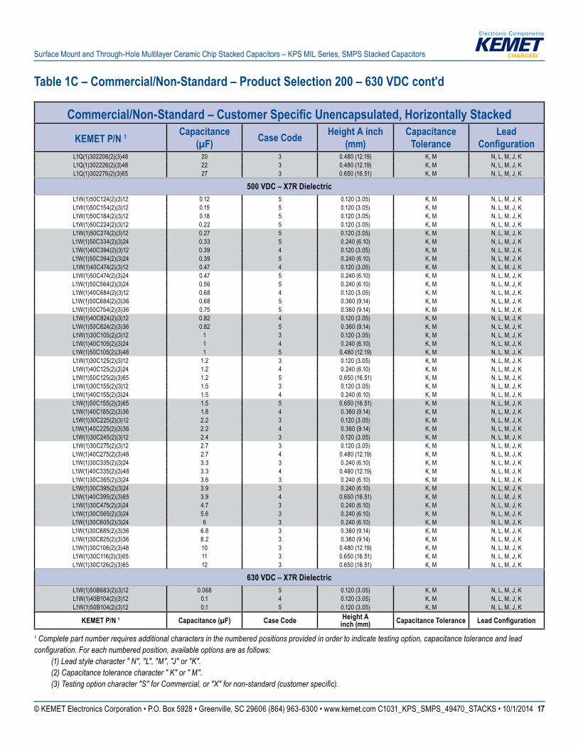
500 VDC – X7R Dielectric L1W(1)50C124(2)(3)12 0.12 5 0.120 (3.05) K, M N, L, M, J, KL1W(1)50C154(2)(3)12 0.15 5 0.120 (3.05) K, M N, L, M, J, KL1W(1)50C184(2)(3)12 0.18 5 0.120 (3.05) K, M N, L, M, J, KL1W(1)50C224(2)(3)12 0.22 5 0.120 (3.05) K, M N, L, M, J, KL1W(1)50C274(2)(3)12 0.27 5 0.120 (3.05) K, M N, L, M, J, KL1W(1)50C334(2)(3)24 0.33 5 0.240 (6.10) K, M N, L, M, J, KL1W(1)40C394(2)(3)12 0.39 4 0.120 (3.05) K, M N, L, M, J, KL1W(1)50C394(2)(3)24 0.39 5 0.240 (6.10) K, M N, L, M, J, KL1W(1)40C474(2)(3)12 0.47 4 0.120 (3.05) K, M N, L, M, J, KL1W(1)50C474(2)(3)24 0.47 5 0.240 (6.10) K, M N, L, M, J, KL1W(1)50C564(2)(3)24 0.56 5 0.240 (6.10) K, M N, L, M, J, KL1W(1)40C684(2)(3)12 0.68 4 0.120 (3.05) K, M N, L, M, J, KL1W(1)50C684(2)(3)36 0.68 5 0.360 (9.14) K, M N, L, M, J, KL1W(1)50C754(2)(3)36 0.75 5 0.360 (9.14) K, M N, L, M, J, KL1W(1)40C824(2)(3)12 0.82 4 0.120 (3.05) K, M N, L, M, J, KL1W(1)50C824(2)(3)36 0.82 5 0.360 (9.14) K, M N, L, M, J, KL1W(1)30C105(2)(3)12 1 3 0.120 (3.05) K, M N, L, M, J, KL1W(1)40C105(2)(3)24 1 4 0.240 (6.10) K, M N, L, M, J, KL1W(1)50C105(2)(3)48 1 5 0.480 (12.19) K, M N, L, M, J, KL1W(1)30C125(2)(3)12 1.2 3 0.120 (3.05) K, M N, L, M, J, KL1W(1)40C125(2)(3)24 1.2 4 0.240 (6.10) K, M N, L, M, J, KL1W(1)50C125(2)(3)65 1.2 5 0.650 (16.51) K, M N, L, M, J, KL1W(1)30C155(2)(3)12 1.5 3 0.120 (3.05) K, M N, L, M, J, KL1W(1)40C155(2)(3)24 1.5 4 0.240 (6.10) K, M N, L, M, J, KL1W(1)50C155(2)(3)65 1.5 5 0.650 (16.51) K, M N, L, M, J, KL1W(1)40C185(2)(3)36 1.8 4 0.360 (9.14) K, M N, L, M, J, KL1W(1)30C225(2)(3)12 2.2 3 0.120 (3.05) K, M N, L, M, J, KL1W(1)40C225(2)(3)36 2.2 4 0.360 (9.14) K, M N, L, M, J, KL1W(1)30C245(2)(3)12 2.4 3 0.120 (3.05) K, M N, L, M, J, KL1W(1)30C275(2)(3)12 2.7 3 0.120 (3.05) K, M N, L, M, J, KL1W(1)40C275(2)(3)48 2.7 4 0.480 (12.19) K, M N, L, M, J, KL1W(1)30C335(2)(3)24 3.3 3 0.240 (6.10) K, M N, L, M, J, KL1W(1)40C335(2)(3)48 3.3 4 0.480 (12.19) K, M N, L, M, J, KL1W(1)30C365(2)(3)24 3.6 3 0.240 (6.10) K, M N, L, M, J, KL1W(1)30C395(2)(3)24 3.9 3 0.240 (6.10) K, M N, L, M, J, KL1W(1)40C395(2)(3)65 3.9 4 0.650 (16.51) K, M N, L, M, J, KL1W(1)30C475(2)(3)24 4.7 3 0.240 (6.10) K, M N, L, M, J, KL1W(1)30C565(2)(3)24 5.6 3 0.240 (6.10) K, M N, L, M, J, KL1W(1)30C605(2)(3)24 6 3 0.240 (6.10) K, M N, L, M, J, KL1W(1)30C685(2)(3)36 6.8 3 0.360 (9.14) K, M N, L, M, J, KL1W(1)30C825(2)(3)36 8.2 3 0.360 (9.14) K, M N, L, M, J, KL1W(1)30C106(2)(3)48 10 3 0.480 (12.19) K, M N, L, M, J, KL1W(1)30C116(2)(3)65 11 3 0.650 (16.51) K, M N, L, M, J, KL1W(1)30C126(2)(3)65 12 3 0.650 (16.51) K, M N, L, M, J, K
630 VDC – X7R Dielectric L1W(1)50B683(2)(3)12 0.068 5 0.120 (3.05) K, M N, L, M, J, KL1W(1)40B104(2)(3)12 0.1 4 0.120 (3.05) K, M N, L, M, J, KL1W(1)50B104(2)(3)12 0.1 5 0.120 (3.05) K, M N, L, M, J, K
KEMET P/N 1 Capacitance (µF) Case Code Height A inch (mm) Capacitance Tolerance Lead Configuration
Table 1C – Commercial/Non-Standard – Product Selection 200 – 630 VDC cont'd
1 Complete part number requires additional characters in the numbered positions provided in order to indicate testing option, capacitance tolerance and lead configuration. For each numbered position, available options are as follows: (1) Lead style character " N", "L", "M", "J" or "K". (2) Capacitance tolerance character " K" or " M". (3) Testing option character "S" for Commercial, or "X" for non-standard (customer specific).

© KEMET Electronics Corporation • P.O. Box 5928 • Greenville, SC 29606 (864) 963-6300 • www.kemet.com C1031_KPS_SMPS_49470_STACKS • 10/1/2014 1818
Surface Mount and Through-Hole Multilayer Ceramic Chip Stacked Capacitors – KPS MIL Series, SMPS Stacked Capacitors
Commercial/Non-Standard – Customer Specific Unencapsulated, Horizontally StackedKEMET P/N 1 Capacitance
(µF) Case Code Height A inch (mm)
Capacitance Tolerance
Lead Configuration
L1W(1)50B124(2)(3)12 0.12 5 0.120 (3.05) K, M N, L, M, J, KL1W(1)50B154(2)(3)12 0.15 5 0.120 (3.05) K, M N, L, M, J, KL1W(1)50B184(2)(3)24 0.18 5 0.240 (6.10) K, M N, L, M, J, KL1W(1)30B224(2)(3)12 0.22 3 0.120 (3.05) K, M N, L, M, J, KL1W(1)40B224(2)(3)12 0.22 4 0.120 (3.05) K, M N, L, M, J, KL1W(1)50B224(2)(3)24 0.22 5 0.240 (6.10) K, M N, L, M, J, KL1W(1)50B274(2)(3)24 0.27 5 0.240 (6.10) K, M N, L, M, J, KL1W(1)30B334(2)(3)12 0.33 3 0.120 (3.05) K, M N, L, M, J, KL1W(1)50B334(2)(3)36 0.33 5 0.360 (9.14) K, M N, L, M, J, KL1W(1)40B394(2)(3)12 0.39 4 0.120 (3.05) K, M N, L, M, J, KL1W(1)50B394(2)(3)36 0.39 5 0.360 (9.14) K, M N, L, M, J, KL1W(1)30B474(2)(3)12 0.47 3 0.120 (3.05) K, M N, L, M, J, KL1W(1)40B474(2)(3)24 0.47 4 0.240 (6.10) K, M N, L, M, J, KL1W(1)50B474(2)(3)36 0.47 5 0.360 (9.14) K, M N, L, M, J, KL1W(1)50B564(2)(3)48 0.56 5 0.480 (12.19) K, M N, L, M, J, KL1W(1)30B684(2)(3)12 0.68 3 0.120 (3.05) K, M N, L, M, J, KL1W(1)40B684(2)(3)24 0.68 4 0.240 (6.10) K, M N, L, M, J, KL1W(1)50B684(2)(3)65 0.68 5 0.650 (16.51) K, M N, L, M, J, KL1W(1)50B754(2)(3)65 0.75 5 0.650 (16.51) K, M N, L, M, J, KL1W(1)40B824(2)(3)24 0.82 4 0.240 (6.10) K, M N, L, M, J, KL1W(1)30B105(2)(3)12 1 3 0.120 (3.05) K, M N, L, M, J, KL1W(1)40B105(2)(3)36 1 4 0.360 (9.14) K, M N, L, M, J, KL1W(1)30B125(2)(3)12 1.2 3 0.120 (3.05) K, M N, L, M, J, KL1W(1)40B125(2)(3)36 1.2 4 0.360 (9.14) K, M N, L, M, J, KL1W(1)30B155(2)(3)12 1.5 3 0.120 (3.05) K, M N, L, M, J, KL1W(1)40B155(2)(3)48 1.5 4 0.480 (12.19) K, M N, L, M, J, KL1W(1)40B185(2)(3)48 1.8 4 0.480 (12.19) K, M N, L, M, J, KL1W(1)30B225(2)(3)24 2.2 3 0.240 (6.10) K, M N, L, M, J, KL1W(1)40B225(2)(3)65 2.2 4 0.650 (16.51) K, M N, L, M, J, KL1W(1)30B245(2)(3)24 2.4 3 0.240 (6.10) K, M N, L, M, J, KL1W(1)30B275(2)(3)24 2.7 3 0.240 (6.10) K, M N, L, M, J, KL1W(1)30B335(2)(3)36 3.3 3 0.360 (9.14) K, M N, L, M, J, KL1W(1)30B365(2)(3)36 3.6 3 0.360 (9.14) K, M N, L, M, J, KL1W(1)30B395(2)(3)36 3.9 3 0.360 (9.14) K, M N, L, M, J, KL1W(1)30B475(2)(3)36 4.7 3 0.360 (9.14) K, M N, L, M, J, KL1W(1)30B565(2)(3)48 5.6 3 0.480 (12.19) K, M N, L, M, J, KL1W(1)30B605(2)(3)65 6 3 0.650 (16.51) K, M N, L, M, J, KL1W(1)30B685(2)(3)65 6.8 3 0.650 (16.51) K, M N, L, M, J, K
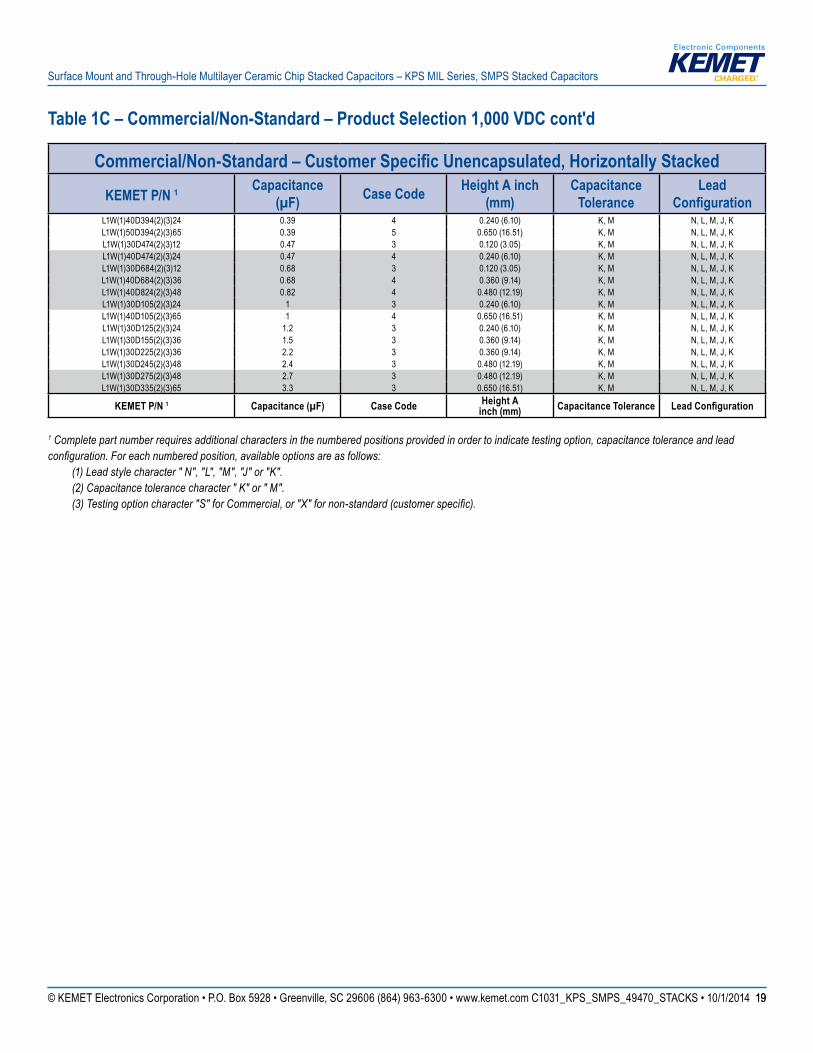
1,000 VDC – X7R Dielectric L1W(1)50D473(2)(3)12 0.047 5 0.120 (3.05) K, M N, L, M, J, KL1W(1)50D683(2)(3)12 0.068 5 0.120 (3.05) K, M N, L, M, J, KL1W(1)30D104(2)(3)12 0.1 3 0.120 (3.05) K, M N, L, M, J, KL1W(1)40D104(2)(3)12 0.1 4 0.120 (3.05) K, M N, L, M, J, KL1W(1)50D104(2)(3)24 0.1 5 0.240 (6.10) K, M N, L, M, J, KL1W(1)50D124(2)(3)24 0.12 5 0.240 (6.10) K, M N, L, M, J, KL1W(1)50D154(2)(3)36 0.15 5 0.360 (9.14) K, M N, L, M, J, KL1W(1)50D184(2)(3)36 0.18 5 0.360 (9.14) K, M N, L, M, J, KL1W(1)30D224(2)(3)12 0.22 3 0.120 (3.05) K, M N, L, M, J, KL1W(1)40D224(2)(3)12 0.22 4 0.120 (3.05) K, M N, L, M, J, KL1W(1)50D224(2)(3)36 0.22 5 0.360 (9.14) K, M N, L, M, J, KL1W(1)50D274(2)(3)48 0.27 5 0.480 (12.19) K, M N, L, M, J, KL1W(1)30D334(2)(3)12 0.33 3 0.120 (3.05) K, M N, L, M, J, KL1W(1)50D334(2)(3)65 0.33 5 0.650 (16.51) K, M N, L, M, J, K
KEMET P/N 1 Capacitance (µF) Case Code Height A inch (mm) Capacitance Tolerance Lead Configuration
Table 1C – Commercial/Non-Standard – Product Selection 630 – 1,000 VDC cont'd
1 Complete part number requires additional characters in the numbered positions provided in order to indicate testing option, capacitance tolerance and lead configuration. For each numbered position, available options are as follows: (1) Lead style character " N", "L", "M", "J" or "K". (2) Capacitance tolerance character " K" or " M". (3) Testing option character "S" for Commercial, or "X" for non-standard (customer specific).
© KEMET Electronics Corporation • P.O. Box 5928 • Greenville, SC 29606 (864) 963-6300 • www.kemet.com C1031_KPS_SMPS_49470_STACKS • 10/1/2014 1919
Surface Mount and Through-Hole Multilayer Ceramic Chip Stacked Capacitors – KPS MIL Series, SMPS Stacked Capacitors
Commercial/Non-Standard – Customer Specific Unencapsulated, Horizontally StackedKEMET P/N 1 Capacitance
(µF) Case Code Height A inch (mm)
Capacitance Tolerance
Lead Configuration
L1W(1)40D394(2)(3)24 0.39 4 0.240 (6.10) K, M N, L, M, J, KL1W(1)50D394(2)(3)65 0.39 5 0.650 (16.51) K, M N, L, M, J, KL1W(1)30D474(2)(3)12 0.47 3 0.120 (3.05) K, M N, L, M, J, KL1W(1)40D474(2)(3)24 0.47 4 0.240 (6.10) K, M N, L, M, J, KL1W(1)30D684(2)(3)12 0.68 3 0.120 (3.05) K, M N, L, M, J, KL1W(1)40D684(2)(3)36 0.68 4 0.360 (9.14) K, M N, L, M, J, KL1W(1)40D824(2)(3)48 0.82 4 0.480 (12.19) K, M N, L, M, J, KL1W(1)30D105(2)(3)24 1 3 0.240 (6.10) K, M N, L, M, J, KL1W(1)40D105(2)(3)65 1 4 0.650 (16.51) K, M N, L, M, J, KL1W(1)30D125(2)(3)24 1.2 3 0.240 (6.10) K, M N, L, M, J, KL1W(1)30D155(2)(3)36 1.5 3 0.360 (9.14) K, M N, L, M, J, KL1W(1)30D225(2)(3)36 2.2 3 0.360 (9.14) K, M N, L, M, J, KL1W(1)30D245(2)(3)48 2.4 3 0.480 (12.19) K, M N, L, M, J, KL1W(1)30D275(2)(3)48 2.7 3 0.480 (12.19) K, M N, L, M, J, KL1W(1)30D335(2)(3)65 3.3 3 0.650 (16.51) K, M N, L, M, J, K
KEMET P/N 1 Capacitance (µF) Case Code Height A inch (mm) Capacitance Tolerance Lead Configuration
Table 1C – Commercial/Non-Standard – Product Selection 1,000 VDC cont'd
1 Complete part number requires additional characters in the numbered positions provided in order to indicate testing option, capacitance tolerance and lead configuration. For each numbered position, available options are as follows: (1) Lead style character " N", "L", "M", "J" or "K". (2) Capacitance tolerance character " K" or " M". (3) Testing option character "S" for Commercial, or "X" for non-standard (customer specific).

© KEMET Electronics Corporation • P.O. Box 5928 • Greenville, SC 29606 (864) 963-6300 • www.kemet.com C1031_KPS_SMPS_49470_STACKS • 10/1/2014 2020
Surface Mount and Through-Hole Multilayer Ceramic Chip Stacked Capacitors – KPS MIL Series, SMPS Stacked Capacitors
Soldering Process
Thecapacitorsandassembliesoutlinedinthisspecificationsheetaresusceptibletothermalshockdamageduetotheirlargeceramicmass.Temperatureprofilesusedshouldprovideadequatetemperatureriseandcool-downtimetopreventdamagefromthermalshock. In general, KEMET recommends against hand soldering for these types of large ceramic devices.
Recommended Soldering Technique: •Solderreflowonly
RecommendedReflowSolderingProfile:
Time
Tem
pera
ture
Tsmin
25° C to Peak
tL
tS
25
tP
Tsmax
TL
TPMax Ramp Up Rate = 2° C/secMax Ramp Down Rate = 2° C/sec
Profile Feature Sn-Pb Assembly
Preheat/SoakTemperature Minimum (TSmin) 100°C Temperature Maximum (TSmax) 150°C
Time (ts) from Tsmin to Tsmax) 60-90 secondsRamp-up rate (TL to TP) 2°C/seconds
Liquidous temperature (TL) 183°CTime above liquidous (tL) 95 secondsPeak Temperature (TP) 240°C
Time within 5°C of maximum peak temperature (tP)
5 seconds
Ramp-down rate (TP to TL) 2°C/secondsTime 25° C to peak temperature 3.5 minutes
Note 1: All temperatures refer to the center of the package, measured on the package body surface that is facing up during assembly reflow
Preheating and Reflow Profile Notes:Due to differences in the coefficient of thermal expansion for the different materials of construction, it is critical to monitor and control the heating and cooling rates during the soldering process. During the reflow soldering process, the maximum recommended heating and cooling rate (dT/dt) is 4°C/second. To ensure optimal component reliability, KEMET's recommended heating and cooling rate is 2°C/second. After soldering, the capacitors should be air cooled to room temperature
before further processing. Forced air cooling is not recommended.

© KEMET Electronics Corporation • P.O. Box 5928 • Greenville, SC 29606 (864) 963-6300 • www.kemet.com C1031_KPS_SMPS_49470_STACKS • 10/1/2014 2121
Surface Mount and Through-Hole Multilayer Ceramic Chip Stacked Capacitors – KPS MIL Series, SMPS Stacked Capacitors
Table 4 – Performance & Reliability: Test Methods and Conditions
Inspection Test MethodTest Level Option
MIL–PRF–49470B Level (B)
MIL–PRF–49470T Level (T)
DSSC Drawing 87106 (C)1
Commercial (S)
Non-Standard (X)2
In-Process InspectionUltrasonic Scanning
(C-SAM) Meet EIA–469 Criteria
Not required Yes (per lot) Not required Not required
Optional per Source Controlled
Drawing (SCD)DPA Analysis EIA–469
In-ProcessVisualInspection
MIL–PRF–49470Method 4.8.3
Group A Requirements
Thermal Shock MIL–STD–202Method 107 Yes (5 cycles) Yes (20 cycles) Yes (5 cycles)
Not required
Optional per Source Controlled
Drawing (SCD)VoltageConditioning
≤200V 500V
MIL–PRF–49470Method 4.8.5.2
200%VR @125°C 120%VR @125°C
Yes (96 hours minimum)
Yes (168 hours minimum)
Yes (96 hours minimum)
VisualandMechanicalInspection
MIL–PRF–49470Method 4.8.4 Yes (per lot)
Yes (per lot)
Yes (per lot) Yes (per lot)
Solderability MIL–STD–202 Method 208
Yes (per Inspection lot)
Yes (per inspection lot)
Optional per Source Controlled
Drawing (SCD)DPA Analysis EIA–469 Not required Not requiredGroup B Requirements
Voltage–TemperatureLimits(TCVC)
MIL–PRF–49470Method 4.8.13.2
Yes (periodic)
Yes (per lot)
Yes (periodic)
Not required
Optional per Source Controlled
Drawing (SCD)
Resistance to Solvents MIL–STD–202Method 215
Terminal Strength MIL–STD–202Method 211
Resistance to Soldering Heat
MIL–STD–202Method 210
Moisture Resistance MIL–STD–202 Method 106
Marking Legibility MIL–PRF–49470Method 4.8.4.1
LowVoltageHumidityTesting
MIL–STD–202 Method 103 Not required Not required
Life Test ≤200V 500V
MIL–STD–202 Method 108
200%VR @125°C 120%VR @125°C
Yes (periodic) Yes (periodic)
Thermal Shock MIL–STD–202Method 107 Not required Not required
KEMET RequirementsVisualandMechanical
Inspection (100%) KEMET Standard Yes Yes Yes Yes YesVoltageConditioning
1 As per discretionary statement outlined in cancelled DSCC Drawing 87106, KEMET will not perform Group B inspections on a per lot basis. KEMET 87106 orders may include a standard certificate of compliance stating compliance to the 87106 requirements, specifically conformance to Group B inspections. Please contact KEMET for additional details
2 Non-standard test level option is designated to satisfy customer specific testing requirements that may deviate from those stated in a Mil-Spec or DSCC drawing.

© KEMET Electronics Corporation • P.O. Box 5928 • Greenville, SC 29606 (864) 963-6300 • www.kemet.com C1031_KPS_SMPS_49470_STACKS • 10/1/2014 2222
Surface Mount and Through-Hole Multilayer Ceramic Chip Stacked Capacitors – KPS MIL Series, SMPS Stacked Capacitors
Product Marking
Capacitors shall be marked with KEMET's name, trademark or (CAGE) code, date, capacitance and capacitance tolerance codes. The date code shall consist of the year and week. For example, the third week of 2011 would be 1103 using a 4-digit date code or 103 using a 3-digit date code. At the option of the manufacturer, the date code may be placed on a separate line. Full marking shall be included on the package.
MIL–PRF–49470 Case code 4 or 5 exampleCapacitor marking will include "JAN" or "J."Case codes 4 and 5 shall be marked with the following sequence of information:J brand (1 digit), product level designator (“B” or “T”) Manufacturer'sidentification(1to5digits)Capacitance code (3 digits) and capacitance tolerance (1 digit)Date code (3 or 4 digits)Case code 3 shall either be fully marked or partially marked like case code 4 or 5 parts at the option of KEMET.
DSCC 87106MarkingshallbeinaccordancewithMIL–STD–1285,exceptthepartsshallbemarkedwiththepartnumberasspecifiedinparagraph1.2 of DSCC Drawing 87106 with the manufacturer's name or code and date code minimum. Case sizes 4 and 5 shall be marked with coded capacitance and tolerance minimum. Full marking shall be included on the package.
Storage and Handling
Ceramic chip capacitors should be stored in normal working environments. While the chips themselves are quite robust in other environments, solderability will be degraded by exposure to high temperatures, high humidity, corrosive atmospheres, and long term storage. In addition, packaging materials will be degraded by high temperature– reels may soften or warp and tape peel force may increase. KEMET recommends that maximum storage temperature not exceed 40ºC and maximum storage humidity not exceed 70% relativehumidity.Temperaturefluctuationsshouldbeminimizedtoavoidcondensationonthepartsandatmospheresshouldbefreeofchlorine and sulfur bearing compounds. For optimized solderability chip stock should be used promptly, preferably within 1.5 years of receipt.
Packaging
Shipping Container Packaging QuantitiesCase Code Small Box Quantity1 (7.5” x 7.5”) Large Box Quantity1 (13.0” x 13.0” )
3 28 104 4 36 144 5 64 225
1 Minimum order value applies. Contact KEMET for details.
JT12345106K1103

© KEMET Electronics Corporation • P.O. Box 5928 • Greenville, SC 29606 (864) 963-6300 • www.kemet.com C1031_KPS_SMPS_49470_STACKS • 10/1/2014 2323
Surface Mount and Through-Hole Multilayer Ceramic Chip Stacked Capacitors – KPS MIL Series, SMPS Stacked Capacitors
Application Notes
Notice of KEMET MIL–PRF–49470 Qualified Products Listing (QPL) Status.KEMET is qualified to supply MIL–PRF–49470/1 unencapsulated X7R Case Codes 3, 4, & 5 ceramic SMPS capacitors in DC voltage ratings of 50 V, 100 V, 200 V, and 500 V. This qualification includes both "B" and "T" test levels.
KEMET is also qualified to supply MIL–PRF–49470/2 encapsulated X7R Case Codes 3, 4, & 5 ceramic SMPS capacitors in DC voltage ratings of 50 V, 100 V, 200 V, and 500 V. This qualification includes "B" level testing only.
Notice of Cancellation: DSCC Drawing 87106 was cancelled on January 3rd 2005.MIL–PRF–49470 parts are preferred and direct replacements.
MIL–PRF–49470 capacitors are preferred over DSCC 87106 capacitors. The MIL–PRF–49470 specification was developed as part of a cooperative effort between the U.S. Military, NASA and the switch mode power supply capacitor manufacturers to produce a robust direct replacement for the DSCC drawing. The military specification product provides additional quality assurance provisions that are NOT required by the DSCC drawing. Two product levels are offered in MIL–PRF–49470: the standard "B" level and the high reliability "T" level. Some of the benefits of the MIL–PRF–49470 product over the 87106 product include the following: Formal qualification process (QPL established), MIL–STD–790 compliance, DSCC audits, routine qualification maintenance testing, i.e., life testing, group A percent defective allowed (PDA) specified, and prohibiting the mixing of chips from different production lots within a single SMPS capacitor stack lot.
MIL–PRF–49470 "T" Level product is recommended for all high reliability applications. MIL–PRF–49470 "T" level product requires the following in-process inspections and additional group A and B screening inspections that are not part of the normal "B" level flow: In-process screening that includes non-destructive internal examination (chip level) and destructive physical analysis (chip level), group A destructive physical analysis (finished stack level), group B lot specific humidity, steady-state, low voltage (lot sample test), and group B lot specific thermal shock and life test (lot sample test).
For additional information regarding KEMET MIL–PRF–49470 QPL status or cancellation of DSCC Drawing 87106, please visit the DSCC website at: www.dscc.dla.mil.

© KEMET Electronics Corporation • P.O. Box 5928 • Greenville, SC 29606 (864) 963-6300 • www.kemet.com C1031_KPS_SMPS_49470_STACKS • 10/1/2014 2424
Surface Mount and Through-Hole Multilayer Ceramic Chip Stacked Capacitors – KPS MIL Series, SMPS Stacked Capacitors
KEMET Corporation World Headquarters
2835 KEMET WaySimpsonville, SC 29681
Mailing Address:P.O. Box 5928 Greenville, SC 29606
www.kemet.com Tel: 864-963-6300 Fax: 864-963-6521
Corporate Offi cesFort Lauderdale, FLTel: 954-766-2800
North America
SoutheastLake Mary, FLTel: 407-855-8886
NortheastWilmington, MATel: 978-658-1663
CentralNovi, MITel: 248-306-9353
WestMilpitas, CATel: 408-433-9950
Mexico Guadalajara, Jalisco Tel: 52-33-3123-2141
Europe
Southern EuropeParis, FranceTel: 33-1-4646-1006
Sasso Marconi, ItalyTel: 39-051-939111
Central EuropeLandsberg, Germany Tel: 49-8191-3350800
Kamen, GermanyTel: 49-2307-438110
Northern EuropeBishop’s Stortford, United Kingdom Tel: 44-1279-460122
Espoo, FinlandTel: 358-9-5406-5000
Asia
Northeast AsiaHong KongTel: 852-2305-1168
Shenzhen, ChinaTel: 86-755-2518-1306
Beijing, ChinaTel: 86-10-5829-1711
Shanghai, ChinaTel: 86-21-6447-0707
Taipei, TaiwanTel: 886-2-27528585
Southeast AsiaSingaporeTel: 65-6586-1900
Penang, MalaysiaTel: 60-4-6430200
Bangalore, IndiaTel: 91-806-53-76817
Note: KEMET reserves the right to modify minor details of internal and external construction at any time in the interest of product improvement. KEMET does not assume any responsibility for infringement that might result from the use of KEMET Capacitors in potential circuit designs. KEMET is a registered trademark of KEMET Electronics Corporation.
© KEMET Electronics Corporation • P.O. Box 5928 • Greenville, SC 29606 (864) 963-6300 • www.kemet.com C1031_KPS_SMPS_49470_STACKS • 10/1/2014 2525
Surface Mount and Through-Hole Multilayer Ceramic Chip Stacked Capacitors – KPS MIL Series, SMPS Stacked Capacitors
DisclaimerAllproductspecifications,statements,informationanddata(collectively,the“Information”)inthisdatasheetaresubjecttochange.Thecustomerisresponsibleforcheckingandverifying the extent to which the Information contained in this publication is applicable to an order at the time the order is placed.
All Information given herein is believed to be accurate and reliable, but it is presented without guarantee, warranty, or responsibility of any kind, expressed or implied.
Statements of suitability for certain applications are based on KEMET Electronics Corporation’s (“KEMET”) knowledge of typical operating conditions for such applications, but are notintendedtoconstitute–andKEMETspecificallydisclaims–anywarrantyconcerningsuitabilityforaspecificcustomerapplicationoruse.TheInformationisintendedforuseonlyby customers who have the requisite experience and capability to determine the correct products for their application. Any technical advice inferred from this Information or otherwise provided by KEMET with reference to the use of KEMET’s products is given gratis, and KEMET assumes no obligation or liability for the advice given or results obtained.
Although KEMET designs and manufactures its products to the most stringent quality and safety standards, given the current state of the art, isolated component failures may still occur. Accordingly, customer applications which require a high degree of reliability or safety should employ suitable designs or other safeguards (such as installation of protective circuitry or redundancies) in order to ensure that the failure of an electrical component does not result in a risk of personal injury or property damage.
Although all product–related warnings, cautions and notes must be observed, the customer should not assume that all safety measures are indicted or that other measures may not be required.