SURFACE-ENHANCED RAMAN SCATTERING FROM SILVER …
196
SURFACE-ENHANCED RAMAN SCATTERING FROM SILVER NANOROD ARRAYS FABRICATED BY OBLIQUE ANGLE DEPOSITION by YONGJUN LIU (Under the Direction of Yiping Zhao) ABSTRACT Surface-enhanced Raman scattering (SERS) has been proven to be a promising and powerful analytical tool in environment monitoring, chemical and biological sensing, disease diagnosing and homeland security checking. This dissertation focuses on the studies on a new SERS substrate platform --- Ag nanorod arrays. We have fabricated Ag nanorod array substrates with different length at various deposition angles using oblique angle deposition (OAD) and the detailed structural characterizations have been performed for these samples. Semi-ordered Ag nanorod arrays have also been fabricated using template OAD method combining with electron beam lithography method. For Ag nanorod array substrates with a fixed stucture, SERS characterizations related to the excitation configuration have been systematically investigated. The SERS intensity strongly depends on the laser incident angle, polarization states and the reflectance from the underlayer of substrates. In order to understand these unique SERS properties, a modified Greenler’s model has been proposed. The theoretical calculations from this model can qualitatively explain these SERS properties. The SERS activity is also strongly dependent on the specific structures, such as length, diameter, and tilted angle of Ag nanorod and so on. For a fixed tilted
Transcript of SURFACE-ENHANCED RAMAN SCATTERING FROM SILVER …
SURFACE-ENHANCED RAMAN SCATTERING FROM SILVER NANOROD ARRAYS
FABRICATED BY OBLIQUE ANGLE DEPOSITION
by
YONGJUN LIU
(Under the Direction of Yiping Zhao)
ABSTRACT
Surface-enhanced Raman scattering (SERS) has been proven to be a promising and
powerful analytical tool in environment monitoring, chemical and biological sensing, disease
diagnosing and homeland security checking. This dissertation focuses on the studies on a new
SERS substrate platform --- Ag nanorod arrays.
We have fabricated Ag nanorod array substrates with different length at various
deposition angles using oblique angle deposition (OAD) and the detailed structural
characterizations have been performed for these samples. Semi-ordered Ag nanorod arrays have
also been fabricated using template OAD method combining with electron beam lithography
method.
For Ag nanorod array substrates with a fixed stucture, SERS characterizations related to
the excitation configuration have been systematically investigated. The SERS intensity strongly
depends on the laser incident angle, polarization states and the reflectance from the underlayer of
substrates. In order to understand these unique SERS properties, a modified Greenler’s model
has been proposed. The theoretical calculations from this model can qualitatively explain these
SERS properties. The SERS activity is also strongly dependent on the specific structures, such as
length, diameter, and tilted angle of Ag nanorod and so on. For a fixed tilted

angle, there exists an optimum length of Ag nanorod for SERS activity. At the same length,
larger SERS intensity can be obtained from a larger tilted angle of Ag nanorods. With the
increase of the diameter of Ag nanorods, the SERS intensity from template Ag nanorods
decreases when the diameter of Ag nanorod is larger than 100 nm.
To understand the SERS mechanism, the origin of SERS from Ag nanorod array has been
investigated. Due to the anisotropic absorbance nature of Ag nanorod layer, our experiments
indicate that most of SERS signal come from the molecules adsorbed on the side surface of Ag
nanorods, not from the so called “hot spots” at the corner of between Ag nanorods and Ag film.
We believe the Ag nanorod absorbance as a function of the thickness plays a critical role.
INDEX WORDS: Surface-enhanced Raman scattering, Silver nanorod, Oblique angle
deposition, Electron beam lithography, Incident angle, Polarization, Reflectance, Greenler’s model, Length, Tiliting angle, Absorbance,Finite difference time domain

SURFACE-ENHANCED RAMAN SCATTERING FROM SILVER NANOROD ARRAYS
FABRICATED BY OBLIQUE ANGLE DEPOSITION
by
YONGJUN LIU
B.S., Huazhong Normal University, China, 1997
M.S., Huazhong University of Science and Technology, China, 2004
A Dissertation Submitted to the Graduate Faculty of The University of Georgia in Partial
Fulfillment of the Requirements for the Degree
DOCTOR OF PHILOSOPHY
ATHENS, GEORGIA
2010

© 2010
Yongjun Liu
All Rights Reserved
SURFACE-ENHANCED RAMAN SCATTERING FROM SILVER NANOROD ARRAYS
FABRICATED BY OBLIQUE ANGLE DEPOSITION
by
YONGJUN LIU
Major Professor: Yiping Zhao
Committee: William M. Dennis Jason Locklin Qun Zhao
Electronic Version Approved: Maureen Grasso Dean of the Graduate School The University of Georgia May 2010

iv
ACKNOWLEDGEMENTS
Upon my PhD thesis defense and graduation, I would like to express my deep gratitude to
my advisor, Dr. Yiping Zhao, for his support, supervision and advice from the very early stage of
this project to the accomplishment of this thesis. Dr. Zhao is a diligent and knowledgeable
mentor. His truly creative thinking, careful attitude, scientist intuition and passion exceptionally
inspire and enrich my growth as a student, a researcher and a scientist want to be. I also express
my appreciations to Dr. William M. Dennis, Dr. Jason Locklin and Dr. Qun Zhao for serving on
my advisory committee.
I am highly thankful to Dr. Richard A. Dluhy, Dr. Jeremy Driskell and Dr. Ximei Qian for
their valuable suggestions. And I also thank Dr. Gregory Book for his kind assistance to use the
facilities in the clean room at Georgia Institute of Technology.
Many thanks go to all my labmates: Dr. Zhongyue Zhang, Dr. Yuping He, Dr. Jianguo
Fan, Dr. Junxue Fu, Dr. Vivien Chu, Dr. Yu Zhu, Mr. Wilson Smith, Mr. John Gibbs and Mr.
Justin Abell, for their helps and discussions in my research.

v
TABLE OF CONTENTS
Page
ACKNOWLEDGEMENTS ........................................................................................................... iv
LIST OF TABLES ....................................................................................................................... viii
LIST OF FIGURES ....................................................................................................................... ix
CHAPTER
1 INTRODUCTION .........................................................................................................1
1.1 Origin of Raman scattering .................................................................................4
1.2 SERS mechanisms ...............................................................................................6
1.3 Localized surface plasmon resonance ...............................................................14
1.4 SERS substrates .................................................................................................29
1.5 Organization of this dissertation ........................................................................37
2 FABRICATION OF SILVER NANOROD ARRAY ..................................................38
2.1 Oblique angle deposition ...................................................................................38
2.2 Ag nanorod arrays fabrication by normal OAD ................................................44
2.3 Template Ag nanorod arrays fabrication ...........................................................49
2.4 Conclusions .......................................................................................................55
3 SERS FROM SILVER NANOROD ARRAYS: EXCITATION CONFIGURATION
DEPENDENCE ...........................................................................................................57
3.1 Incident angle dependence ................................................................................58

vi
3.2 Underlayer effect ...............................................................................................62
3.3 Polarization dependence ....................................................................................65
3.4 Modified Greenler’s model ...............................................................................69
3.5 Conclusions .......................................................................................................87
4 SERS FROM SILVER NANOROD ARRAYS: SUBSTRATES STRUCTRAL
PARAMETERS DEPENDENCE ................................................................................88
4.1 Length dependence of SERS from Ag nanorod arrays .....................................88
4.2 Diameter and separation dependence of SERS from template Ag nanorod
arrays .................................................................................................................98
4.3 Conclusions .....................................................................................................105
5 THE ORIGIN OF SERS FROM SILVER NANOROD ARRAY .............................107
5.1 Electric field “hot spots” .................................................................................108
5.2 Experimental design to locate Raman probe molecules ..................................110
5.3 The SERS enhancement factor at different substrate locations ......................112
5.4 Polarization dependence of SERS signal ........................................................113
5.5 The layer absorbance model ............................................................................114
5.6 Conclusions .....................................................................................................117
6 CONCLUSION AND FUTURE WORK ..................................................................119
REFERENCES ............................................................................................................................122
APPENDICES .............................................................................................................................148
A GREENLER’S MODEL ............................................................................................148
B SEPARATION DEPENDENCE OF SERS FROM GOLD NANOPOST ARRAY .154

vii
C SHAPE DEPENDENCE OF SERS FROM GOLD NANOROD ARRAY AND
NANOCOMB ARRAY .............................................................................................162
D FINITE DIFFERENCE TIME DOMAIN NUMERICAL METHOD .......................171
viii
LIST OF TABLES
Page
Table 1.1: Comparison of different techniques which could potentially fabricate uniform,
reproducible and large area SERS substrates ................................................................31
Table C.1: The ratio of experimental SRES intensity and the normalized overall local field
enhancement ratio rodcomb II '/' at different detection configuration for different
nanostructures ..............................................................................................................165
Table C.2: The ratio of normalized local field enhancement ratio rodcomb II '/' at different detection
configuration for different surfaces of the nanostructures ..........................................169

ix
LIST OF FIGURES
Page
Figure 1.1: Illustration of Rayleigh scattering, Raman scattering and IR absorbance ....................2
Figure 1.2: The oscillating dipole model of molecule .....................................................................4
Figure 1.3: Illustration of EM mechanism for SERS .......................................................................8
Figure 1.4: (a), (b) and (c) are the E-fields distribution and enhancement contours for a rod,
spheroid and triangular prism, and the arrows show locations with the maximum of E-
filed ................................................................................................................................10
Figure 1.5: E-field distribution of (a) Au nanoring and (b) Au nanophotonic crescent moon ......10
Figure 1.6: (a) and (b) E-field distribution of Ag nanosphere dimmer and 3D plot of E-field
enhancement; (c) and (d) E-field distribution of Ag triangular prism dimmer and 3D
plot of E-field enhancement ..........................................................................................12
Figure 1.7: E-field distributions of dimmers of nanospheres and nanoshell, (b) T-shaped dimmer
consisting of a sphere and a hemispherically capped rod..............................................12
Figure 1.8: SEM images of (i) monomers through pentamers of 120 ± 10 nm Au disks with 30 ±
5 nm separations. (ii) Au disk with identical 30 ± 5 nm separations and thicknesses of
40 ± 5, 80 ± 8, 120 ± 10, and 200 ± 15 nm from top left to bottom right. At the top left
is a single Au disk (thickness 40 nm). (iii) Identical 120 ± 10 nm Au disks with
separations of 160 ± 10, 80 ± 10, 30 ± 5, 15 ± 5, and 5 ± 2 nm from bottom left to top
right. (iv), (v), (vi), are 3D confocal Raman images of the structures shown in (i), (ii)
and (iii). Numbers indicate intensity in arbitrary units .................................................13

x
Figure 1.9: (A) Full multibowtie structure, with seven nanoconstrictions. (B) Close-up of an
individual constriction after electromigration. Note that the resulting nanoscale gap (<
5 nm at closest separation, as inferred from closer images) is toward the right edge of
the indicated red square. (C) Map of Si Raman peak (integrated from 500 to 550 cm-1)
in device from (B), with red corresponding to high total counts. The attenuation of the
Si Raman line by the Au electrodes is clear. (D) Map of pMA SERS signal for this
device based on one carbon ring mode (integrated from 1050 to 1110 cm-1). (E) Map
of integrated low-energy background (50-300 cm-1) for this device .............................14
Figure 1.10: (a) Schematic diagram of a surface propagating plasmon; (b) Schematic diagram of
a localized surface plasmon ...........................................................................................15
Figure 1.11: The calculated extinction spectra of a spheroid, a rod, and a triangular prism with
the same effective radius ~15 nm. The aspect ratios of spheroid and rod are 3.4:1 and
2.8:1, respectively. The prism has a 60 nm edge dimension with thickness of 12 nm .15
Figure 1.12: Sketch of a homogeneous sphere placed into an electrostatic field ..........................16
Figure 1.13: (a) E-field contours for radius 30 nm Ag sphere in vacuum excited at wavelength
369 nm; (b) Comparison of extinction efficiency, surface-averaged E-field
enhancement, and E-field enhancement for specific points for radius 30 nm Ag spheres
in a vacuum ...................................................................................................................18

xi
Figure 1.14: (a) Unpolarized dark-field scattering spectra and corresponding SEM images of
single isolated particles of different diameters (D = 50, 100, 150 and 200 nm). The
dashed lines show Lorentzian fits of the experimental data and solid lines show
scattering spectra calculated on the basis of the MLWA polarizability. (b)
Experimental LSPR peak vs. particle diameter. The solid and dashed lines show
MLWA results for oblate spheroids with heights of 20 and 25 nm, respectively. The
substrate is taken into account through an effective refractive index of 1.25 ...............20
Figure 1.15: UV-vis absorption spectra of 9, 22, 48, and 99 nm gold nanoparticles in water. All
spectra are normalized at their absorption maxima, which are 517, 521, 533, and 575
nm, respectively .............................................................................................................20
Figure 1.16: Exact electrodynamic calculation of the extinction spectra of oblate spheroids with a
sphere radius of 80 nm. The major to minor axis ratio is from left to right: 10, 5, 3.33,
2.5, 2, 1.67, 1.43, 1.25, 1.11, and 1 ...............................................................................21
Figure 1.17: Near- field intensity as a function of wavelength for an electromagnetic plane wave
incident on a cylindrical Au nanorod. L is the length of the nanorod. The rod radius R
is 40 nm. The near field is evaluated 1 nm from the nanorod. Results for small L are
shown in the insets ........................................................................................................21
Figure 1.18: The TEM images and the spectral peak wavelength for three different shapes
(sphere, pentagon and triangle) of individual silver nanoparticles with three different
size .................................................................................................................................22
xii
Figure 1.19: Dark-field spectra and SEM images of isolated D ≈ 95 nm, h ≈ 25 nm particle pairs
with varying separations in parallel and perpendicular polarization, as indicated by
arrows. The separations (gaps) between the particles are d ≈ (A) 10, (B) 15, (C) 25,
(D) 50, and (E) 250 nm. Spectrum (F) from a single particle is included for
comparison ....................................................................................................................24
Figure 1.20: LSP peak position for pairs in parallel polarization geometry versus surface
separation d. The particle diameters were D ≈ 80 or 90 nm, and the height h ≈ 25 nm.
Each point represents an average over ~ 20 pairs. The full and broken lines show DDA
and CDA calculations, respectively, for the same particle and illumination geometry as
in the measurements ......................................................................................................24
Figure 1.21: (a) Normalized near-field intensity at the midpoint between two nanorods as a
function of wavelength for an excitation light incident on a pair of cylindrical Au
nanorods, s is the separation between the nanorods. L = 200 nm, R = 40 nm. The
polarization is parallel to the rod; (b) Dependence of the near-field of an isolated rod
and a dimmer of Au nanorods on the interrod gap s for an excitation light with
polarization parallel to the rods for both at midpoint and in the gap 1 nm from the end
of a rod ...........................................................................................................................25
Figure 1.22: Extinction spectra of a single silver sphere radius 50 nm and a one-dimensional
array of 400 × 50 nm spheres spaced by 470 nm, with polarization and wavevector
both perpendicular to the array axis ..............................................................................26

xiii
Figure 1.23: (a) Extinction spectra of 50 nm silver nanoparticles in a one dimensional chain of
400 particles, the polarization vector and wave vector are both perpendicular to the
chain; (b) a two-dimensional hexagonal array of 400 particles, the wave vector is
perpendicular to the plane and the polarization vector is in the plane ..........................26
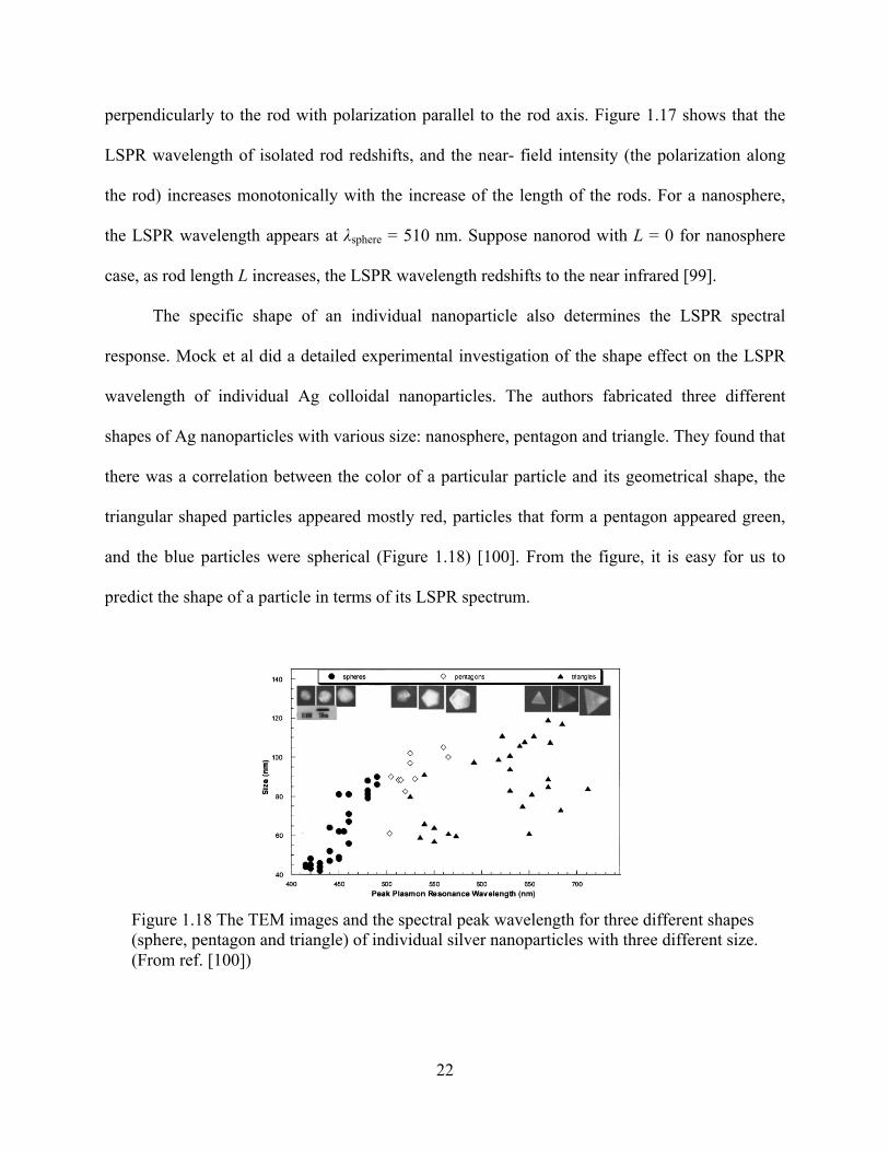
Figure 1.24: (a) SEM image of Ag particle pad on glass with an interparticle spacing of 632 nm,
diameter = 130 nm, height = 30 nm; (b) show the darkfield measurements for samples
with 2 interline spacing and cylinder diameters of 130, taken of arrays varying in
interparticle spacing from 400 to 700 nm with a uniform refractive index (n = 1.5)
around the particles. The corresponding single particle spectra are shown (dotted line)
with peak positions of λmax = 660 nm ............................................................................27
Figure 1.25: Variation of the LSPR wavelength with the diameter of cylinders (open circle) or
the length of ellipsoids major axis (full circle). Inset: SEM images of typical arrays of
ellipsoidal (minor axis: 50 nm, major axis: 120 nm, height: 50 nm) and cylindrical
(diameter: 100 nm, height: 50 nm) particles achieved by EBL. The gap between two
nanoparticles is kept constant at 200 nm .......................................................................28
Figure 1.26: SEM images of several representative SERS substrates ...........................................30
Figure 1.27: Relative substrate efficiency vs d, quantified as ISERS(d)/ISERS(dmax), for two
different adsorbates: R6G and thiophenol. Insets show examples of Raman spectra for
different d values and SEM image of sphere array .......................................................32
Figure 1.28: (a) SEM image of Au nanorod array, scalar bar represents 2 µm; (b) SERS peak
intensity at band 1200 cm-1 Raman mode versus the nanowire aspect ratio R = L/l and
the nanowire length for experimental data (plain square) and for FDTD calculations
(open circle) ...................................................................................................................33

xiv
Figure 1.29: (a) AFM morphologies of the Au nanorod arrays. The average pore diameter of the
AAO template was ~66 nm; (b) Reflectance spectra of the Au nanorod array substrates
with the indicated pore diameters; (Arrow points to the excitation laser wavelength
488 nm); (c) SERS signal ratio as a function of Au nanorod diameter .........................34
Figure 1.30: (a) SEM images of various Ag nanoparticle aggregates; (b) and (c) Polar plots of the
Raman intensity of spot A and spot C versus polarization. The Raman intensity scale
(a.u.) corresponds to 500 and 2000 counts per division in (b) and (c), respectively .....35
Figure 1.31: (a) Extinction spectra of an ellipsoidal particle array for two polarization states of
the incident light, parallel and perpendicular to the major axis; (b) Raman (open circle)
and LSPR (mode along the major axis located at 750 nm, full circle) intensity plotted
against the polarization angle; the solid line is the cos2 fit ..........................................36
Figure 1.32: (a) SEM images of Ag nanowire monolayers with varying degrees of order. The
order parameter, S, characterizes the overall orientation alignment of the sample, with
perfect alignment for S = 1: (a) S = 0.970; Scale bar = 1 µm. The inset shows a TEM
image of the nanowires, with pentagonal cross sections and an atomically smooth
surface. Scale bar = 50 nm; (b) Polar plot of SERS intensities for various low-
frequency Raman bands with respect to polarization angle. The dark lines represent the
best fit to a periodic cosine function. ............................................................................36
Figure 2.1: (a) A schematic of oblique angle deposition; (b) and (c) Shadowing effect ...............39
Figure 2.2: Cross section SEM images of nanorods of different material fabricated by OAD
technique under different deposition conditions ...........................................................40

xv
Figure 2.3: The initial vapor nucleates on the seeds and their shadows enforce periodic
nucleation, and yield a periodic columnar structure when the OAD is performed on a
seeds pattern ..................................................................................................................42
Figure 2.4: Schematics of seeds pattern .........................................................................................44
Figure 2.5: The top-view (up) and cross-section (down) SEM images of Ag nanorod arrays with
length L ≈ 1200 nm prepared at θ = 78°, 80°, 82°, and 84°, respectively .....................46
Figure 2.6: (a) The plot of Ag nanorod height h versus the Ag nanorod length L for samples
deposited at θ = 78°, 80°, 82°, and 84°, respectively ; (b) The Ag nanorod tilt angle β
as a function of deposition angle θ ................................................................................47
Figure 2.7: The log-log plots of the diameter D (a) and the density n (b) of Ag nanorod versus
the length L for various deposition angles θ ..................................................................48
Figure 2.8: sketch of Au nanopost array fabrication process by EBL ...........................................51
Figure 2.9: The top view SEM images of Au nano-post array seed patterns with the designed
diameter: (a) D = 100 nm, (b) D = 120 nm and (c) D = 140 nm, respectively. The scale
bars in the figures are the same .....................................................................................52
Figure 2.10: The top view SEM images of Ag nanorods on (a) blank Si substrate (D =0), and on
Au nano-post array seed patterns with the designed diameter, (b) D = 100 nm, (c) D =
120 nm and (d) D = 140 nm, respectively. ....................................................................53
Figure 2.11: The sum of the diameter and separation of the Ag nanorods as a function of the sum
of diameter and separation of Au nano-posts ................................................................55
Figure 3.1: (a) and (b) SEM images of the top and cross-sectional view of Ag nanorod array ....58
Figure 3.2: Illustration of Ag nanorod array and incident configuration .......................................59

xvi
Figure 3.3: The sketch of Enwave Raman probe and the setup of the incident angle dependence
measurement ..................................................................................................................59
Figure 3.4: Representative SERS spectra of BPE adsorbed on Ag nanorod substrate at different
incident angles, ϕ = -10 o, 0o, 20 o, 45 o, and 60 o respectively. The peak intensity was
strongest at around 45° ..................................................................................................61
Figure 3.5: The integrated SERS intensity for the BPE band at 1200 cm-1 plotted as a function of
the incoming laser incident angle ..................................................................................62
Figure 3.6: The reflectance spectra of underlayers ........................................................................63
Figure 3.7: The representative SERS spectra obtained from Ag nanorod arrays on different
underlayers ....................................................................................................................64
Figure 3.8: The SERS peak intensity I1200 as a function of reflectance from underlayers ............65
Figure 3.9: Diagram of definition of incident light polarization ...................................................66
Figure 3.10: Polarized SERS spectra of BPE on the Ag nanorod substrates .................................67
Figure 3.11: Polar plots of the SERS peak intensity at Raman band Δv = 1200 cm-1 of BPE as a
function of polarization angle ψ ....................................................................................68
Figure 3.12: (a) Representative absorbance spectra from Ag nanorod rod array excited by
different polarization light; (b) Polar plot of the relationship between the absorbance
and polarization angles ..................................................................................................69
Figure 3.13: A schematic illustration of the modified Greenler’s model. (a) Case I, the dipole is
in the incident plane; (b) Case II, the dipole is perpendicular to the incident plane. All
the induced dipoles are perpendicular to the nanorod ...................................................74

xvii
Figure 3.14: The relative Raman intensity Ramanη as a function of the incident angle θ calculated
from the modified Greenler’s model for an Ag nanorod SERS substrate. The
underlayer substrate is Ag, the excitation light is unpolarized, and the nanorod tiling
angles are β = 63º, 65º, 67º), 70º, and 72º, respectively ................................................81
Figure 3.15: The SERS peak intensity as a function of the incident angle (scattered points), and
the ratio of Raman scattering intensity to the incident light intensity calculated from
the modified oscillating dipole model (solid curve) ......................................................82
Figure 3.16: The optimal incident angle 0ϕ as a function of Ag nanorod tilting angle β under
unpolarized excitation light ...........................................................................................83
Figure 3.17: The relative Raman intensity Ramanη as a function of incident angle ϕ for different
underlayer thin films: Ag thin film; Ti thin film, Si wafe, and glass substrate The
nanorod tilting angle is fixed, °= 70β .........................................................................84
Figure 3.18: The SERS peak intensity as function of reflectance from underlayers .....................84
Figure 3.19: The polarization dependence SERS intensity at different incident angles °= 0ϕ
(navy filled circles), 15o (black filled squares), 30o (blue triangles), 45o (green
pentagons), 60o (red stars), and 75o (orange diamonds), respectively. When the
incident angles ϕ are smaller than 15o, the SERS intensity reaches a maximum at
polarization angle of 90o, and 270 o. When the incident angles are bigger than 15o, the
SERS intensity reaches a maximum at polarization angles of 0o and 180o ...................86
Figure 4.1: (a) The reflectance spectra of Ag nanorod arrays with different length L deposited at
θ = 84; (b) the reflectance R and absorbance A at λ = 785 nm as a function of nanorod
length L; and (c) the spectra of the effective absorbance coefficient α for Ag nanorod
arrays with different lengths deposited at θ = 84° .........................................................90

xviii
Figure 4.2: The incident and transmission configurations for SERS signal detection for the Ag
nanorod array SERS substrate. This sketch illustrates the coordinates to calculate the
effective EF based on the phenomenological model .....................................................90
Figure 4.3: (a) The reflectance spectra of Ag nanorod arrays with a fixed length L= 1200 nm
prepared at different deposition angles; and (b) the reflectance R and absorbance A at λ
= 785 nm as a function of deposition angles θ ..............................................................92
Figure 4.4: (a) The SERS EF as a function of nanorod length L for samples deposited θ = 78°,
80°, 82°, and 84°, respectively; and (b) the SERS EF as a function of deposition angle
θ at a fixed nanorod length L = 165 nm ........................................................................93
Figure 4.5: (a) The SERS EF versus the reflectance R785 at λ = 785 nm from the Ag nanorod
array samples with different nanorod length and prepared at different deposition
angles; and (b) the SERS EF versus the reflectance R785 from samples with a fixed
nanorod length L = 1200 nm and L = 164 nm prepared at different deposition angles θ,
respectively ....................................................................................................................95
Figure 4.6: Sketches of three different configurations for the SERS experiments, (a) Case I, a 1
μL drop of 10-4 M concentration of BPE is spread on Au nano-post array patterns; (b)
Case II, Ag nanorods are deposited onto the samples from Case I; (c) Case III, a 1 μL
drop of 10-5 M concentration of BPE is placed onto the samples from case II .............99
Figure 4.7: The absorbance spectra of 800 nm Ag nanorod on glass ..........................................100
Figure 4.8: (a), (b) and (c) show the representative SERS spectra obtained from different
patterned substrates for Case I, Case II, and Case III, respectively ............................100

xix
Figure 4.9: (a) The Raman peak intensities at Δv = 1200 cm-1 I1200 as functions of the diameter Dr
and and separation dr of Au nano-post for Case III, respectively, (b) The Raman peak
intensities at Δv = 1200 cm-1 I1200 as a function of the sum l of Dr the diameter Dr and
and separation dr of Au nano-post ...............................................................................102
Figure 5.1: (a) A SEM image of Ag nanorod array; (b) A diagram of the 3 × 3 Ag nanorod array
model; (c) and (d) are the E-field distribution under p-polarization incidence in the xz
plane and yz plane, respectively ..................................................................................109
Figure 5.2: An illustration of the three different samples designed to illustrate the effect of “hot
spots” on the SERS spectra of Ag nanorod arrays, (a) Case I. A 1 μL drop of 10-4 M
BPE was put onto a Ag film; (b) Case II. Ag nanorods were deposited by oblique
angle vapor deposition onto the samples in Case I; (c) Case III. A 1 μL drop of 10-5 M
BPE was placed onto the sample in Case II ................................................................111
Figure 5.3: (a) The representative SERS spectra obtained from samples prepared in Case I, II and
III;(b) The representative spectra obtained from different polarization excitation at 633
nm in Case II and Case III ...........................................................................................113
Figure 5.4: (a) The representative SER spectra of substrates without the Ag film for Case II and
Case III at λ = 785 nm with two different excitation and collection configurations; (b)
The representative SERS spectra of substrates without the Ag film for Case II and
Case III under the excitation of two different polarization at λ = 633 nm with two
different excitation and collection configurations .......................................................116
Figure A.1: Geometry of the excitation light incident on a planar interface ...............................149
Figure A.2: The sketches of geometries of three possible orientation for an oscillating dipole on a
planar surface relative observation point .....................................................................151

xx
Figure B.1: (a), (b) and (c) are three top view SEM images of Au nanopost array with the
diameter D = 100 nm, and separation d = 60 nm, 160 nm and 235 nm, respectively.
The scale bar represents 200 nm for all SEM images .................................................156
Figure B.2: Representative SERS spectra of BPE obtained from the Au nanopost arrays with
different separation d = 85 nm, 110 nm, 135nm, 180 nm, and 235 nm, respectively.
The spectra are not normalized to the post number .....................................................157
Figure B.3: (a) The relative SERS peak intensity per post at Δν =1200 cm-1 (star), 1604 cm-1
(filled circle) and 1636 cm-1(filled square), and the rescaled sum of <E>4 versus d
calculated by FDTD method (the solid curves); (b) the enhancement of edge EEI , and
top TEI , and the total enhancement EI , as functions of the separation d, calculated by
FDTD method ..............................................................................................................159
Figure B.4: (a) The top view and (b) the cross-sectional view of the local E-field distribution of
the 3×3 nanopost array calculated by FDTD method ..................................................160
Figure C.1: Top view SEM images of (a) Au nanorod array and (b) Au nanocomb array .........163
Figure C.2: Representative SERS spectra of MGITC obtained from (a) Au nanorod array and (b)
Au nanocomb array at λ = 785 nm, and under s-polarization and p-polarization at λ =
633 nm .........................................................................................................................164
Figure C.3: The local E-field distribution excited at λ = 633 nm for p-polarization (a) and s-
polarization (b) of Au nanorod array, and for p-polarization (c) and s-polarization (d)
of Au nanocomb array. The dashed squares in (a) and (c) show different surfaces of
the two nanostructures: ① end surface; ② side surface; ③ top surface ....................167
Figure D.1: Illustration of a standard Cartesian Yee cell for FDTD ...........................................173
1
CHAPTER 1
INTRODUCTION
Vibrational spectroscopy is a very old spectroscopic method, it corresponds to the
molecular vibrational transition, hence can be used to obtain molecular structure and dynamics
information. At the beginning of 20th century, infrared (IR) absorbance was first applied to study
the interactions between the light and matter, thereby producing the first vibrational spectrum.
For a very long time, vibrational spectroscopy was only limited to apply on analysis of fairly
small molecules until the invention of laser in the 1960s. With the laser used as light sources, it
became possible to perform experiments on the large and rather complex molecular systems, and
the application of vibrational spectroscopy to biomolecule and life science achieved many
breakthroughs. Recently, the vibrational spectroscopy has been widely applied in life science
researches such as the identification of bacteria and virus [1-7], drug distribution monitoring in
live cell [8, 9] tumor targeting [10-12] and so on.
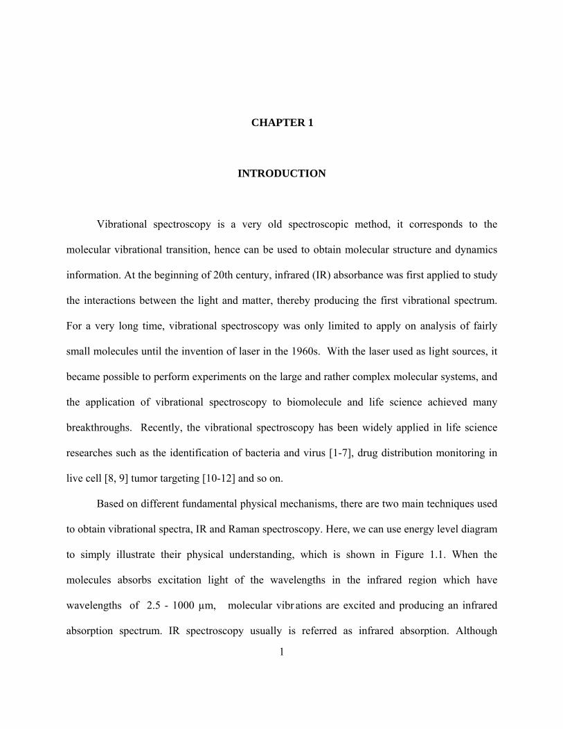
Based on different fundamental physical mechanisms, there are two main techniques used
to obtain vibrational spectra, IR and Raman spectroscopy. Here, we can use energy level diagram
to simply illustrate their physical understanding, which is shown in Figure 1.1. When the
molecules absorbs excitation light of the wavelengths in the infrared region which have
wavelengths of 2.5 - 1000 µm, molecular vibr ations are excited and producing an infrared
absorption spectrum. IR spectroscopy usually is referred as infrared absorption. Although
2
infrared spectroscopy was discovered much earlier than Raman spectro scopy and was
dominant for a long time in spectroscopy methods, IR spectroscopy has some limitations. For
example, some vibrations are inherently weak in IR, the sample preparation is time-consuming,
and especially the studies of biological components in aqueous solution are difficult in IR
spectroscopy method. Raman scattering is observed by Indian scientist C. V. Raman in liquids
and by Russian physicists G. S. Landsberg and L. I. Mandelstam in crystals in 1928
independently [13]. When the excitation monochromatic light impinges on the molecule, the
molecule experiences a energy transition, excited from a ground state to an intermediate energy
level (virtual energy level), after it relaxes, it emits a photon and the molecule returns to a
different vibrational energy state. If the final state is more energetic than the initial state, then the
emitted photon will be shifted to a lower frequency than the excitation photon, this shift in
frequency is defined as a Stokes shift; if the final state is less energetic than the initial state, then
the emitted photon will be shifted to a higher frequency than the excitation photon, this shift in
frequency is designed as a Anti-Stokes shift. Both Stokes and anti-Stokes scattering are Raman
scattering. For a given molecule, the induced vibrational transitions occur with different
Figure 1.1 Illustration of Rayleigh scattering, Raman scattering and IR absorbance
Virtual energy state
Infrared
Absorption
0 1 2 3 Vibrational
Energy State
Electronic state
Rayleigh
scattering
Stokes Raman
scattering
Anti-Stokes Raman
scattering
3
probabilities, hence there are different vibrational bands,displayed in Raman spectra. Compared
to IR absorbance, Raman spectroscopy has following advantages: Since Raman peaks are much
narrower than IR bands, it generates highly compound-specific and molecular structure
information for chemical analysis; it shows a great potential for multi-component analysis;
especially, Raman spectroscopy can work on aqueous samples because water itself does not give
any Raman signal. The Raman technique also requires little sample preparation, which allows
field applications. Therefore, Raman spectroscopy is an excellent complement spectroscopy
method to IR [14]. But the intensity of conventional Raman spectroscopy is very low, because
the Raman cross-section is inherently weak at 10-29 cm2. This limitation drastically prevents the
practical applications of the Raman spectroscopy, especially in the detection of organic and bio-
molecules.
Fortunately, in 1974 Fleischman et al first reported that “Giant Raman scattering of
pyridine adsorbed on roughed Ag electrode” [15]. This phenomenon is called surfaced-enhanced
Raman scattering (SERS). After the first observations of the SERS effect, Van Duyne [16],
Gersten [17], Aravind [18], Kerker [19], Moskovits [20], Schatz [21] and others have performed
an extensive amount of fundamental and theoretical researches on this effect. But, due to the
limitation of the enhancement ~103 – 106, most studies involved samples with concentrations
between 10-1 and 10-3 M. Those concentrations are much larger than the concentration ranges for
trace analysis, and SERS have not leaded to practical applications until 1997 [17, 19, 22]. With
the rapid development of nanotechnology, various nanostructures fabricated by different
techniques have been used as SERS-active platforms to generate higher SERS enhancement
factor (EF) [23-41]. In 1997, Nie et al [42] and Kneipp et al [43] independently reported that the
SERS EF could reach 1013-1014, which brought an enormous resurgence of interest in SERS. In

4
recent years, SERS has been a popular field of great scientific and even clinic interest, and the
SERS technique has become a fast, promising and powerful analytical tool in environmental
monitoring [44-47], chemical and biological sensing [1, 7, 48-51], disease diagnosing [52, 53],
and homeland safety [54, 55].
1.1 Origin of Raman scattering
A simple classical model can illustrate most of the essential features of Raman scattering.
If a molecule is exposed in an excitation light with a frequency exv , the molecule can be treated
as an oscillating dipole, which is shown in Figure 1.2. Suppose the excitation electric field E of
the light is an alternating electric field
)2cos(0 tvEE exπ= , (1.1)
the induced dipole moment μ in the molecule is given by
Eαμ = , (1.2)
where α is the polarizability of the molecule. The polarizability is a material property which
( tEE ex= πν2cos0
( )tqq vib= πν2cos0
?
Figure 1.2 The oscillating dipole model of a molecule
)

5
depends on the molecular structure and the nature of the bonds. For any molecular bond, the
individual atoms are confined to specific vibrational modes. The vibrational energy of a
particular mode is given by
vibvib hvjE )( 21+= , (1.3)
where j is the vibrational quantum number (j = 0,1,2…), vibv is the frequency of the vibrational
mode, and h is the Planck constant. Assume that q is the physical displacement of atoms about
their equilibrium position due to a particular vibrational mode, it can be simply written as
)2cos(0 tvqq vibπ= , (1.4)
where 0q is the vibrational amplitude about equilibrium position. Because the ability to perturb
the local electron cloud of a molecular structure depends on the relative location of the individual
atoms, the polarizability is a function of the displacement of constituent atoms. For a small
displacement, the polarizability can be approximately expanded by a Taylor series as
qq q0
0 ∂∂
+=ααα , (1.5)
where 0α is the polarizability of the molecule at the equilibrium nuclear geometry. With
equation (1.4), the polarizability can be written as
)2cos(00
0
tvqq vib
q
πααα∂∂
+= . (1.6)
Substituting equation (1.1) and (1.6) into (1.2), the induced dipole moment is given by
)2cos()2cos()2cos( 0000
0
tvtvEqq
tvE exvibq
ex ππαπαμ∂∂
+= . (1.7)
Using a trigonometric identity, equation (1.7) can be rewritten as

6
]})(2cos[])(2{cos[2
)2cos( 0000
0
tvvtvvEqq
tvE vibexvibexq
ex ++−∂∂
+= ππαπαμ . (1.8)
Equation (1.8) implies that the induced dipole moments are composed of oscillations with three
different frequencies exv , vibex vv − , vibex vv + , which results in scattered radiation at these three
frequencies. The first term includes a radiation with the excitation frequency exv . Thus, this term
describes the elastic scattering, i.e. Rayleigh scattering or Mie scattering. The second term
describes radiations with frequencies vibex vv − and vibex vv + , which referred to the scattered
photons that gains or loses energy compared to the excitation photon. These two radiations are
inelastic scattering due to Raman scattering. The lower frequency ( vibex vv − ) radiation is referred
to as Stokes scattering, and the higher frequency ( vibex vv + ) radiation is referred to Anti-Stokes
scattering. Equation (1.8) also gives a selection rule, because the second term also depends on
the factor 0qq∂
∂α . If this derivative equals zero, the second term will be zero and there will be no
Raman scattering. Thus, the selection rule is: A molecular motion will be Raman-active only if
the motion occurs with a changing polarizability. Although the normal Raman cross section is
extermely weak, it is possible to enhance the cross section by changing 0qq∂
∂α and 0E according
to equation (1.8).
1.2 SERS mechanisms
Equation (1.8) shows that the Raman intensities are the product of the incident E-field
intensity and polarizability differentiation. To enhance the Raman signal, one can improve these
two parameters. Therefore, two primary mechanisms are believed to be responsible for SERS,
7
one involves enhancements in the field intensity as a result of localized plasmon resonance
excitation, and the other relates to the enhancement in polarizability differentiation due to
chemical effects, although these two mechanisms usually entangles to contribute to the SERS.
The first one is called a long-range classical electromagnetic (EM) mechanism and the second
one is called a short-range chemical (CHEM) mechanism [20, 56-59]. These two mechanisms
usually contribute simultaneously to the overall enhancement.
1.2.1 Chemical mechanism of SERS
The chemical enhancement can be divided into two enhancement mechanisms:
the chemical bonding effect [60] and charge-transfer mechanisms [61-63]. The chemical
bonding effect is mainly caused by the formation of metal-molecular complexes due to the
chemical bonding. In this mechanism, there are several factors contributing to the enhancement
of Raman scattering: relative orientation of molecule with respect to the metal cluster, the local
symmetry of the chemisorbed molecule, and the proximity of the particular vibrational mode to
the binding site. Saikin et al showed that the SERS EF from benzenethiol chemisorbed on Ag
clusters due to chemical bonding effect can reach 103 [60]. The charge-transfer happens between
the metal and the adsorbed molecule due to the electron excitation.One possible reason
contributing to the SERS EF is that the transferred charge affects the surface plasmon modes and
change the surface plasmon contribution to light scattering by metal surface, then enhance the
Raman scattering; another reason is that virtual excitations to the charge transfer state, which can
be partially resonant with the exciting radiation, yield large contributions to the Raman scattering
[63]. The charge-transfer effect can generally contribute to SERS EF with 10 - 103 [61-66]. But
recently Fromm et al reported that a small number of p-mercaptoaniline molecule on a single

8
bowtie showed the chemical enhancement > 107, likely due to the charge-transfer between the
Au surface and molecule [67]. In fact, the chemical mechanism is not fully understood. It is also
very hard to experimentally study the chemical mechanism of SERS for the systems which
support electromagnetic enhancement, because the chemical mechanism is never independent,
while the two effects are multiplicative for the systems.
1.2.2 Electromagnetic mechanism of SERS
Since the chemical enhancement is generally about 10 - 103 and there is no chemical
effect of SERS for most molecules [68], the EM mechanism is considered to contribute the most
to the observed Raman intensity enhancement. This enhancement is due primarily to the local
electric field enhancement by the excitation of localized surface plasmon resonance of a
particular nanostructure, such as nanoparticles. As shown in Figure 1.3, when the excitation
field )(0 exvEv
with frequency exv incidents onto a nanoparticle, the excited nanoparticle will
generate the electric field )( exlm vEv
over the surface, the total electric field over the surface of the
particle is called the localized electric field or primary field )()()( 0 exlmexexl vEvEvEvvv
+= . If the
molecules are adsorbed on this location of the surface of the particle, they will be excited by the
localized electric field with magnitude )( exl vE , and the corresponding excited molecules radiate
)(0 exvE
)( exlm vE
o)( Rdip vE
)( Rsc vE
Figure 1.3 Illustration of EM mechanism for SERS

9
the scattered Raman electric field (also called secondary electric field) )( Rdip vEv
with frequency
Rv . The nanoparticle can also be further excited by the secondary electric field )( Rdip vEv
and
radiated electric field )( Rsc vEv
at frequency Rv . Therefore, the total Raman scattered electric field
)()()( RscRdipRR vEvEvEvvv
+= with magnitude )( RR vE . Assume that )( exvg is the averaged local
field enhancement over the surface of the particle, the average magnitude of localized electric
field lE will be expressed as )()()( 0 exexexl vEvgvE = . )()()()( 0 exexexlRdiv vEvgvEvE αα , where
α is the appropriate polarizability tensor. Therefore the Raman scattered electric fields can be
further enhanced by the nanoparticles in exactly the same way as the incident field does. Assume
that the Raman scattered electric field is enhanced by a factor )( Rvg . Thus, the final amplitude
of the Raman scattered field also called SERS scattered field will be written as
)()()()( 0 exexRRSERS vEvgvgvE α , (1.9)
and the overall SERS intensity will be
022 )()( IvgvgI RexSERS α , (1.10)
where SERSI and 0I are the SERS intensity and excitation laser intensity, respectively.
Since vvv exR Δ+= , when vΔ is small and exvv <<Δ , )()()()(
0 ex
exlRex vE
vEvgvg =≈ . Define
)()()(
0 ex
exlexl vE
vEvgg == , the SERS intensity will be enhanced by a factor proportional to the fourth
power of the enhancement of the local electric field [19, 20, 69], i.e.,
442 )()()( lexRex gvgvgvgG === , (1.11)
where G is defined as the SERS enhancement factor (EF). Since 0E is a constant and ll E ,g
the SERS EF is proportional to the fourth power of the local electric field, 4lEG .

10
The locations with largest electric field enhancements are called “hot spots”. In general,
the enormous enhancement of the Raman scattering is believed to originate from the “hot spots”
in nanoparticle systems. The “hot spots” are also considered to be responsible for the single
molecule sensitivity of SERS [42, 43, 70]. “Hot spots” particularly exist at the tips of
nanoparticles or in the junctions with an intense electric field induced by the interparticles
coupling effect. For example, the two ends of Au or Ag nanorods, and the corners of triangular
shaped Au or Ag nanoparticles, the small gaps (on the order of a few nanometers) between Au
2 4 6 8 10 12 14
Figure 1.5 E-field distribution of (a) Au nanoring from ref. [75] and (b) Au nanophotonic crescent moon from ref. [76]
(a) (b)
(a) (b) (c) Figure 1.4 (a), (b) and (c) are the E-fields distribution and enhancement contours for a Ag nanorod, nanospheroid and nanotriangular prism, and the arrows show locations with the maximum of E-field. (From ref. [74])

11
or Ag nanoparticle aggregates (dimers, trimers, or larger aggregates) can all be viewed as “hot
spots” [71-74]. Hao et al have theoretically studied the E-field distributions from Ag nanorod
with an effective diameter 30 nm, an aspect ratio of 2.8 : 1, an oblate spheroid with an effective
diameter 30 nm, an aspect ratio of 3.4 : 1 and triangular prism with side length 60 nm, snip 0
nm, and thickness 12 nm. For these three nanoparticles, the longest wavelength plasmon
resonance is near 700 nm. The E-field contours show that the maximum enhancement for the
dipole resonances occurs at the tips of particles (Figure 1.4). The largest possible fields intensity
<E2> enhancement for the plasmon resonance are 4500 for the rod, 4700 for the spheroid, and
3500 for the triangular prism [74]. Aipurua et al analyzed the E-field enhancement around the
Au nanoring excited at wavelength λ = 1000 nm. The diameter of the ring was 120 nm, the
thickness of the belt was 10 nm, and the height of the ring was 22.7 nm. The authors set the
excitation E-field direction as left-to-right. They found that the maximum of E-field occurred at
upper and lower of nanoring along E-field, and the largest E-field intensity enhancement was
2500 (Figure 1.5(a)) [75]. Lee et al found that the SERS enhancement factor could be larger than
1010 at the sharp edge of Au nanophotonic crescent moon (r = 150 nm, R = 200 nm, and d = 51
nm) excited at wavelength λ = 785 nm (Figure 1.5(b)) [76]. From those examples, it is well
known that “hot spots” usually locate at the end, tip, or corner of specific metallic nano objects.
For the “hot spots” of dimer and trimer nanoparticle systems, Xu et al found that the SERS
enhancement could reach 1010 at the midpoint between two nanospheres (diameter D = 90 nm)
with an edge-to-edge separation d = 1 nm, at the excitation wavelength λ = 514.5 nm [72]. Hao
et al did a detailed theoretical study on the field enhancement for dimer of spheres and triangular
prisms, the largest SERS enhancement was estimated to be 1.21 × 10⁸ under excitation at the
wavelength of 520 nm for dimer of spheres with diameter 36 nm, while the largest SERS

12
enhancement could be 2.8 × 10⁹ under excitation at resonance wavelength 932 nm for dimer of
triangular prisms with edge dimension 60 nm, the spacing for both dimer was 2 nm (Figure 1.6)
[74]. Tally et al experimentally and theoretically investigated the “hot spots” of an adjacent
nanoshell pair with a 3 nm interparticle distance, and the SERS enhancement was estimated to
be 5.2 × 10⁷. They also compared this result with the largest SERS enhancement (3.4 × 10⁶)
from dimer of nanospheres (D = 60 nm) with the same separation (Figure 1.7(a)) [77]. Camden
et al studied SERS EF distribution around a T-shaped dimer consisting of a sphere and a
Figure 1.6 (a) and (b) E-field distribution of Ag nanosphere dimer and 3D plot of E-field enhancement; (c) and (d) E-field distribution of Ag triangular prism dimer and 3D plot of E-field enhancement. (From ref. [74])
(a) (b) (c) (d)
1
100
Figure 1.7 (a) E-field distributions of dimers of nanospheres (top) and nanoshells (bottom) from ref. [77], (b) T-shaped dimer consisting of a sphere and a hemispherically capped rod from ref. [73].
(a) (b)

13
hemispherically capped rod that just touch together (0 nm separation). They found that the
maximum SERS EF reached 3.9 × 10⁸ at wavelength of 532 nm, and the hot spot was near, but
not at the intersection of the two particles, i.e., at the particle junction (Figure 1.7(b)) [73].
Experimentally, “hot spots” of some nanostructure systems can be observed through Raman
imaging or mapping [78-80]. Laurent et al observed Raman scattering image for Au nanoring
array fabricated by electron beam lithography. Their diameters were 1 µm and 2 µm, and the
excitation wavelength was 647 nm [80]. Qin et al studied nanodisk arrays fabricated by a so-
called on-wire lithography method and recorded Raman images of “hot pots” for these structures
at λ = 633 nm (Figure 1.8). The authors made direct comparisons between different types of
dimmers, trimmers and tetramers of varying gap spacing and thickness from 3D confocal Raman
images of the structures [79, 81]. Ward et al used Raman map of Si (integrated from 500 to 550
cm-1) and SERS map of para-mercaptoaniline (pMA) (integrated from 1050 to 1110 cm-1)
Figure 1.8 SEM images of (i) monomers through pentamers of 120 ± 10 nm Au disks with 30 ± 5 nm separations. (ii) Au disk with identical 30 ± 5 nm separations and thicknesses of 40 ± 5, 80 ± 8, 120 ± 10, and 200 ± 15 nm from top left to bottom right. At the top left is a single Au disk (thickness 40 nm). (iii) Identical 120 ± 10 nm Au disks with separations of 160 ± 10, 80 ± 10, 30 ± 5, 15 ± 5, and 5 ± 2 nm from bottom left to top right. (iv), (v), (vi), are 3D confocal Raman images of the structures shown in (i), (ii) and (iii). Numbers indicate intensity in arbitrary units. OWL-Generated nanodisk arrays from ref. [79, 81]

14
studied “hot spots” distribution for multibowtie structure (Figure 1.9) [82]. From above
examples, the “hot spots” around the nano-sized structural systems are usually generated by the
localized surface plasmon excitation due to the specific nanoscale topologies of the metal
nanostructures [72].
1.3 Localized surface plasmon resonance
When the material (a metal) has a large negative real and small positive imaginary
dielectric constant such as noble metals (Ag, Au and Cu) excited by an electromagnetic radiation,
the free electrons can oscillate collectively. These oscillations occur at the plasma frequency and
the associated quanta are called plasmons. As shown in Figure 1.10(a), at a planar interface
between a metal and a dielectric, the plasmon is confined on the surface and propagating along
Figure 1.9 (A) Full multibowtie structure, with seven nanoconstrictions. (B) Close-up of an individual constriction after electromigration. Note that the resulting nanoscale gap (< 5 nm at closest separation, as inferred from closer images) is toward the right edge of the indicated red square. (C) Map of Si Raman peak (integrated from 500 to 550 cm-1) in device from (B), with red corresponding to high total counts. The attenuation of the Si Raman line by the Au electrodes is clear. (D) Map of pMA SERS signal for this device based on one carbon ring mode (integrated from 1050 to 1110 cm-1). (E) Map of integrated low-energy background (50-300 cm-1) for this device. (From ref. [82])

15
the interface direction (x direction), hence called surface Plasmon (also called surface
propagating plasmon). If the electrons experience a resonant coherent oscillation with the
frequency of the excitation light, this is called surface plasmon resonance (SPR). When the size
of a metal structure is within 100 nm, the oscillation of electrons is restricted at a localized
surface. This confined plasmon is called the localized surface plasmon (LSP) shown in Figure
1.10(b). For the case of LSP, the excitation light interacts with particles much smaller than the
excitation wavelength. This can lead to a plasmon that oscillates locally at the surface of the
Electric field
Metal sphere (a) (b) Dielectric
Metal
x
z
Electron cloud
Figure 1.10 (a) Schematic diagram of a surface propagating plasmon; and (b) Schematic diagram of a localized surface plasmon. (From ref. [83])
Figure 1.11 The calculated extinction spectra of a spheroid, a rod, and a triangular prism with the same effective radius ~15 nm. The aspect ratios of spheroid and rod are 3.4:1 and 2.8:1, respectively. The prism has a 60 nm edge dimension with thickness of 12 nm. (From ref. [74])

16
nanoparticle with a frequency known as LSP resonance (LSPR) [83]. If the frequency of the light
matches with the collective oscillations frequency of confined electrons, the light excited a LSPR,
and the nanoparticle system will absorb maximum energy from the excitation light, which
corresponds to an absorbance peak in the absorbance spectrum. This absorbance peak is called
the LSPR peak and the corresponding wavelength is named the LSPR wavelength pλ . Figure
1.11 shows typical extinction spectra of a Ag nano spheroid, a Ag nanorod, and a Ag nano
triangular prism mentioned in above section, the plasmon peak for all three nanoparticles
700=pλ nm [74].
However, it is very hard to get an analytical solution to understand the localized surface
plasmons for most systems. For some ideal nanoparticle systems such as nanospheres,
nanospheroids and nanorods, it is possible to directly calculate the electric field distribution and
then calculate the absorbance coefficient analytically based on classic electrodynamics. In order
to further understand the theory of localized surface plasmon resonance, we will give a very
simple example --- a spherical nanoparticle of radius R shown in Figure 1.12. Suppose the
nanosphere is irradiated by x-polarized light of wavelength λ. The radius R of the sphere is much
smaller than the excitation wavelength λ. In this limit, the nanosphere can be treated to be
P
Εen
R
x
E0
Εm
Figure 1.12 Sketch of a homogeneous sphere placed into an electrostatic field.

17
immersed in an electrostatic field. The solution for the electric and magnetic field outside the
particle is given by
)]ˆˆˆ(3ˆ[]
2[ˆ),,( 530
30 zzyyxx
rx
rxERxEzyxE
enm
enmout ++−
+−
−=εε
εε , (1.12)
where εm = εr + iεi and εen are the dielectric constant of the metal nanoparticle and the external
environment, respectively. E0 is the magnitude of incident electric field. Equation (1.12)
describes the near-fields at the particle surfaces quite accurately for small enough particles.
However, the far field beyond 100 nm from the center of the particle exhibits radioactive
contributions that are not contained in this equation. To describe far field, the dipole field should
be replaced by its radioactive counterpart. In the case of the dipole field, this is given by
5
2
32 )(3[)1()(
rPrrPrrike
rPrrekE ikrikr
dipole
vvvvv
vvv ⋅−−+
××= , (1.13)
where Pv
is the dipole moment of the nanoparticles. In the limit: 0→k , equation (1.13) reduces
to the static field in equation (1.12). Figure 1.13(a) presents contour of the electric field
enhancement around 30 nm radius Ag sphere in xz plane. The excitation wavelength of 369 nm
was the dipole plasmon peak of 30 nm Ag nanosphere. Since the dipole field dominates, a
characteristic p-orbital shape is shown around the sphere in Figure 1.13(a). At the long range, the
radioactive terms in equation (1.13) become more important, and the field has a characteristic
spherical wave. Figure 1.13(b) plots the surface-average E-field enhancement for the 30 nm
sphere as a function of wavelength, along with the extinction efficiency. This figure shows the E-
field enhancement at two specific points on the surface of the sphere: point 1 is along the
polarization direction, and point 2 located 45° away from the polarization direction. The E-field
enhancement associated with point 1 is about three times larger than the surface average value,
while point 2 shows a smaller enhancement and corresponding LSPR peak also blue shifted a

18
little compared to point 1 [71]. From equation (1.12), the extinction spectra of the metal sphere
can also be calculated as follows
])())((
)([)10ln(
24)( 22
2332
λεχελελε
λεπλ
ienr
ienNRE++
= , (1.14)
where the factor χ depends on the particle geometries. We can only analytically solve χ value
for spheres ( χ = 2) and spheroids. But for most nanoparticle systems, they are too complicated to
obtain an analytical χ value, the numerical methods are employed to solve these problems such
as multiple multipole approximation (MMP) [84-86], discrete dipole approximation (DDA) [87-
89], and finite difference time domain (FDTD) methods [90-95].
From equation (1.12), when εm ~ -2εen, the outside EM field is extremely enhanced
relative to the incident field. Recall equation (1.11), the SERS enhancement factor can written as
40
22 )()(
E
vvEvEEFSERS
outout Δ−= . (1.15)
From above understanding, the LSPR response from any nanoparticle system is sensitive
to the size, shape, interparticle spacing, dielectric environment, and dielectric properties of the
metallic nanoparticles. To further illustrate these LSPR characteristics, the following examples
(a) (b)
2 1
Figure 1.13 (a) E-field contours for radius 30 nm Ag sphere in vacuum excited at wavelength 369 nm; (b) Comparison of extinction efficiency, surface-averaged E-field enhancement, and E-field enhancement for specific points for radius 30 nm Ag spheres in a vacuum. (From ref. [71])
19
will mainly discuss LSPR dependences of the size, separation and shape of several nanoparticle
systems: isolated particle, particle pairs and particle arrays.
1.3.1 Isolated nanoparticle
Several basic shapes of isolated particle system (sphere, spheroid, nanorod, pentagon and
triangle) have been studied. The LSPR response strongly depends on both size and shape of
particles. The above discussion gave a detailed description of E-field distribution and extinction
spectra of isolated nanosphere. Here, examples on size dependence of LSPR wavelength will be
introduced. With the increase of the size of the nanoparticle, the LSPR wavelength is red-shifted
[71, 96-98]. Gunnarsson et al did a theoretical and experimental study on the size dependence of
LSPR for nanodisks fabricated by electron beam lithography. The particle diameters D were
varied from 30 to 200 nm, and the height h of the particles was estimated to be in the range of 20
- 25 nm. The LSPR wavelength changed from 450 nm to 900 nm, and the wavelength shift is
approximately 27 nm per 10 nm change in diameter for the nanodisks [97]. Figure 1.14(a) shows
the scattering spectra of single isolated Ag particles with the diameters of D = 50, 100, 150, and
200 nm. Figure 1.14(b) plotted the LSPR wavelength as a function of diameter for oblate
spheroids with heights of 20 and 25 nm, respectively, and it is almost a linearly increasing
function of the size. The authors also used modified long wavelength approximation (MLWA)
polarizability to calculate the scattering efficiency. In Figure 1.14(a), the solid curves show
scattering spectra calculated on the basis of MLWA polarizability. Link et al also experimentally
observed the absorbance spectra of Au nanospherical particles in aqueous solution by UV-vis
spectrometer (Figure 1.15). The average diameters of nanospherical particles were 9 nm, 22 nm,
48 nm and 99 nm, respectively. From the absorbance spectra, the LSPR peak position redshifted

20
with the increase of the diameter of Ag nanoparticles [96]. Kelly et al theoretically studied
extinction spectra of oblate Ag spheroids. The authors used Mie theory to perform an exact
electrodynamics calculation of the extinction spectra of oblate spheroids [71]. Figure 1.16 shows
Figure 1.14 (a) Unpolarized dark-field scattering spectra and corresponding SEM images of single isolated particles of different diameters (D = 50, 100, 150 and 200 nm). The dashed lines show Lorentzian fits of the experimental data and solid lines show scattering spectra calculated on the basis of the MLWA polarizability. (b) Experimental LSPR peak vs. particle diameter. The solid and dashed lines show MLWA results for oblate spheroids with heights of 20 and 25 nm, respectively. The substrate is taken into account through an effective refractive index of 1.25. (From ref. [97])
Figure 1.15 UV-vis absorption spectra of 9, 22, 48, and 99 nm gold nanoparticles in water. All spectra are normalized at their absorption maxima, which are 517, 521, 533, and 575 nm, respectively. (From ref. [96])

21
extinction efficiency spectra for oblate Ag spheroids calculated by an exact analytical theory.
The excitation electric field polarization was along the major axis of the spheroid. The ratio of
major to minor axes vary from 1 (sphere) to 10 (highly oblate) [71]. Aizpurua et al theoretically
investigated electric near- and far- field distributions of Au nanorods with a diameter of 80 nm,
hemispherical, rounded ends. Since the LSPR wavelength has similar trend of size dependence
for both near- and far- field. We can take near-field as example. The excitation light incidents
Figure 1.16 Exact electrodynamic calculation of the extinction spectra of oblate spheroids with a sphere radius of 80 nm. The major to minor axis ratio is from left to right: 10, 5, 3.33, 2.5, 2, 1.67, 1.43, 1.25, 1.11, and 1. (From ref. [71])
Figure 1.17 Near- field intensity as a function of wavelength for an electromagnetic plane wave incident on a cylindrical Au nanorod. L is the length of the nanorod. The rod radius R is 40 nm. The near field is evaluated 1 nm from the nanorod. Results for small L are shown in the insets. (From ref. [99])
22
perpendicularly to the rod with polarization parallel to the rod axis. Figure 1.17 shows that the
LSPR wavelength of isolated rod redshifts, and the near- field intensity (the polarization along
the rod) increases monotonically with the increase of the length of the rods. For a nanosphere,
the LSPR wavelength appears at λsphere = 510 nm. Suppose nanorod with L = 0 for nanosphere
case, as rod length L increases, the LSPR wavelength redshifts to the near infrared [99].
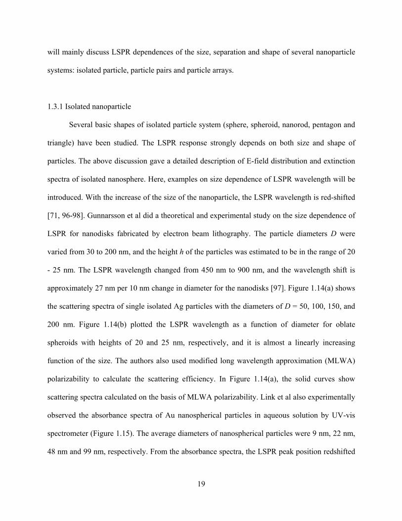
The specific shape of an individual nanoparticle also determines the LSPR spectral
response. Mock et al did a detailed experimental investigation of the shape effect on the LSPR
wavelength of individual Ag colloidal nanoparticles. The authors fabricated three different
shapes of Ag nanoparticles with various size: nanosphere, pentagon and triangle. They found that
there was a correlation between the color of a particular particle and its geometrical shape, the
triangular shaped particles appeared mostly red, particles that form a pentagon appeared green,
and the blue particles were spherical (Figure 1.18) [100]. From the figure, it is easy for us to
predict the shape of a particle in terms of its LSPR spectrum.
Figure 1.18 The TEM images and the spectral peak wavelength for three different shapes (sphere, pentagon and triangle) of individual silver nanoparticles with three different size. (From ref. [100])

23
1.3.2 Nanoparticle pairs
When two particles are placed close enough to make LSPR spectra and E-field
distributions extremely different from an isolated particle, such a particle system is called a
dimer. In a dimer system, the E-field intensity could achieve a large enhancement, especially in
the middle point of two particles excited along the dimer axis, compared to any location of an
isolated particle with the same diameter. Therefore, the separation between nanoparticles plays
an important role in the LSPR response. With the increase of separation, the peak position
rapidly blue-shifts [72, 97, 99, 101, 102]. Gunnarsson et al also theoretically and experimentally
studied the interparticle interactions of the dimer of the nanospherical particles. They changed
the separation of the dimer and found LSPR wavelength for polarization parallel to the dimer
axis exhibited a strong redshift as the interdimer separation decreased. The diameter of the
spherical particle was 95 nm and the height was 25 nm. The separation was chose to be 10 nm,
15 nm, 25 nm, 50 nm and 250 nm (Figure 1.19) [97]. From Figure 1.19, when the spacing
between two particles became large enough, the LPSR response from the dimer was more close
to the LSPR response from the isolated particle, therefore, the dimmer system can be treated as
an isolated particle system. The authors also used DDA and CDA to calculate the LSPR
wavelength for parallel polarization along the dimer axis by varying the gap of the dimers with
two different diameters D = 80 and 95 nm. Figure 1.20 plotted the LSPR peak position as a
function of separation of the dimer [97]. Aizpurua et al also investigated the coupling effect by
changing the separation of the dimer of Au cylindrical nanorods. The shape of rod was
mentioned when we discussed isolated particle, but the length was 200 nm. The excitation light
polarized parallel to the rod axis. Figure 1.21(a) shows the change in the near-field responses at
midpoint between the rods when the separation s between rods was varied to modify the

24
coupling. As the separation increased, the LSPR wavelength blue shifts and the E-field
magnitude decreased. Figure 1.21(b) plotted the E-field as a function of edge-to-edge separation
Figure 1.20 LSP peak position for pairs in parallel polarization geometry versus surface separation d. The particle diameters were D ≈ 80 or 90 nm, and the height h ≈ 25 nm. Each point represents an average over ~ 20 pairs. The full and broken lines show DDA and CDA calculations, respectively, for the same particle and illumination geometry as in the measurements. (From ref. [97])
Figure 1.19 Dark-field spectra and SEM images of isolated D ≈ 95 nm, h ≈ 25 nm particle pairs with varying separations in parallel and perpendicular polarization, as indicated by arrows. The separations (gaps) between the particles are d ≈ (A) 10, (B) 15, (C) 25, (D) 50, and (E) 250 nm. Spectrum (F) from a single particle is included for comparison. (From ref. [97])
Scat
terin
g (a
rb. u
nits
)
Wavelength (nm) Wavelength (nm) Wavelength (nm) 400 500 600 700 800 900 400 500 600 700 800 900 400 500 600 700 800 900

25
s of the dimmer of Au nanorods. With decreasing separation s, the E-field increased rapidly due
to the coupling of the two Au nanorods [99].
1.3.3 Nanoparticle arrays
Since two close particles can change the LSPR response and achieve a large E-field
enhancement, well-defined particle arrays also attract great interest of researchers and scientists.
In Schatz’s group, Zhao et al and Zou et al performed systematic theoretical studies on the LSPR
response of nanoparticle arrays [103-105]. They found that one dimensional array structures built
from spherical Ag nanoparticles with a radius of 50 nm produced remarkablely narrow plasmon
resonance spectra upon excitation with light that was polarized perpendicular to the array axis
(Figure 1.22) [106]. As shown in Figure 1.22, the LSPR spectrum of one dimensional particle
array is much narrower than that of isolated particle. Zou et al also investigated two dimensional
array and distance dependence of LSPR spectra for particle arrays, which is shown in Figure
(a) (b)
Figure 1.21 (a) Normalized near-field intensity at the midpoint between two nanorods as a function of wavelength for an excitation light incident on a pair of cylindrical Au nanorods, s is the separation between the nanorods. L = 200 nm, R = 40 nm. The polarization is parallel to the rod; (b) Dependence of the near-field of an isolated rod and a dimmer of Au nanorods on the interrod gap s for an excitation light with polarization parallel to the rods for both at midpoint and in the gap 1 nm from the end of a rod. (From ref. [99])

26
1.23. For one dimensional array containing 400 particles with radius 50 nm, with the increase of
the center-to-center distance from 100 nm to 700 nm, the LSPR spectra redshifts and
become narrower and narrower. But narrow resnonances are only found for polarization
perpendicular to the array axis. For the two dimensional arrays, the variation in the
Figure 1.22 Extinction spectra of a single silver sphere radius 50 nm and a one-dimensional array of 400 × 50 nm spheres spaced by 470 nm, with polarization and wavevector both perpendicular to the array axis. (From ref. [106])
Figure 1.23 (a) Extinction spectra of 50 nm silver nanoparticles in a one dimensional chain of 400 particles, the polarization vector and wave vector are both perpendicular to the chain; (b) a two-dimensional hexagonal array of 400 particles, the wave vector is perpendicular to the plane and the polarization vector is in the plane. (From ref. [104])
(a) (b)
27
plasmon peak with increasing particle separation is very similar to that in the 1D chains, but the
plasmon is always broader than that of 2D arrays. The excitation light incidented perpendicularly
to the arrays with polarization parrallel to the array [104]. They also reported that 1D
nanoparticle arrays can combine local field enhacement of nanoparticle dimmers with long range
photonic interactions leading to giant enhancements ( |E|2 > 107) at specific locations [106].
Experimentally, Hicks et al. demonstrated the plasmon line shapes of linear Ag arrays of
cylindrical nanoparticles fabricated by EBL [107]. As shown in Figure 1.24(a), the cyllinder
diameter was 130 nm, the spacing varied from 400 nm to 700 nm, and the interline spacing was 2
µm. The author found that as the interparticle distance increased toward the single particle
resonance wavelength, the shoulder on the red portion of the line shape narrowed and became
Figure 1.24 (a) SEM image of Ag particle pad on glass with an interparticle spacing of 632 nm, diameter = 130 nm, height = 30 nm; (b) show the darkfield measurements for samples with 2 interline spacing and cylinder diameters of 130, taken of arrays varying in interparticle spacing from 400 to 700 nm with a uniform refractive index (n = 1.5) around the particles. The corresponding single particle spectra are shown (dotted line) with peak positions of λmax = 660 nm. (From ref. [107])

28
more intense, with a maximum intensity occurring at spacing of 625 nm. With further larger
spacings, the LSPR peak remained narrow, but the intensity decreased until it dissapeared in the
spectrum (Figure 1.24(b)). For two dimensional nanoparticle arrays, the LSPR wavelength
dependence of the diameter and separation of nanoparticle system has been widely studied. For
example, Grand et al studied size dependence of LSPR walength for cylinders array and ellipse
array fabricated by EBL. They obtianed the LSPR wavelength red shifted with the increase of the
size (Figure 1.25) [108].
From above examples and discussions, LSPR plays an important role in enhacing local
electric field, and LSPR wavelength strongly depends on the size, shape, separation and
environmental medium of particle systems. Therefore, we can engineer SERS substrates in terms
Figure 1.25 Variation of the LSPR wavelength with the diameter of cylinders (open circle) or the length of ellipsoids major axis (full circle). Inset: SEM images of typical arrays of ellipsoidal (minor axis: 50 nm, major axis: 120 nm, height: 50 nm) and cylindrical (diameter: 100 nm, height: 50 nm) particles achieved by EBL. The gap between two nanoparticles is kept constant at 200 nm. (From ref. [108])

29
of the correlation of the effects of the size, shape, separation and envionmental medium of
nanoparticle.
1.4 SERS substrates
1.4.1 The fabrication methods of SERS substrates
The Raman intensity enhancement attributed to the SERS mechanism is primarily due to
the enhancement of localized electric field [83]. Therefore, a critical aspect of SERS is the
requirement of a specific morphology to alter the local electric field and achieve reproducible
and high level of enhancement. Most of reports on SERS substrates use gold, silver and copper
because of their negative dielectric constants. It has also been demonstrated that some other
metals such as transition metals (e.g., Pt, Ru, Rh, Pd, Fe, Co, Ni, and their alloys) were used to
fabricate SERS substrates [109], but the SERS effect from these materials are too low to be of
practical applications. A large number of methods have been used to fabricate and synthesize
nanostructures as SERS substrates. For examples, chemical methods such as oxidation-reduction
cycles (ORC) (Fleischmann et al 1974) [15], metal colloid hydrosol (Ahern et al 1986) [110],
chemical etching (Xue et al 1991) [111], laser ablation of metals (Neddersen et al 1993) [112],
and chemical synthesis of Ag or Au nanoparticles (Nie et al, Kneipp et al in 1996) [42, 43];
physical methods such as physical vapor deposition (Schlegel et al 1991, Roark et al 1996) [113,
114] and mechanical polishing (Taylor et al 1996) [115]. Most fabrication techniques only focus
on obtaining large SERS enhancements, but the requirements for practical applications are
seldom considered. In particular, Au and Ag nanoparticle aqueous solution have been used
extensively to study SERS because they can provide huge enhancements (~1014) and are easy to
synthesize in solution [42, 43]. However this type of nanoparticle structure fabricated by

30
chemical synthesis is limited due to the nature of particle aggregation and particle co-location,
although some methods are adopted to improve reproducibility [116]. This limitation leads to a
poor reproducibility of samples especially when dried onto inert substrates (Figure 1.26(a)) [117].
Currently, there are mainly following four fabrication methods which can potentially produce
more uniform and reproducible SERS substrates to meet the specific requirements: the template
method, nanosphere lithography (NSL), electron beam lithography (EBL), and oblique angle
deposition method. The template method employs a porous structure array such as anodic porous
alumina mask as template to deposit Ag or Au nanorods directly into the pores by
electrochemical plating or physical vapor deposition methods (Figure 1.26(b)) [29, 32, 118, 119].
Van Duyne and coworkers are pioneers to use NSL to fabricate SERS substrates. In this
technique, nanospheres/microspheres were self-assembled into a monolayer or bilayer on the
(a) (b) (c)
(d) (e) (f)
(Murphy et al [117]) (kondo et al [32]) (Van Duyn et al [122])
(Liu et al [90]) (Liu et al [135]) (Nicholas et al [26])
Figure 1.26 SEM images of several representative SERS substrates
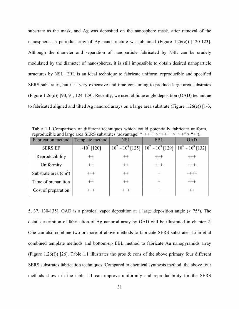
31
substrate as the mask, and Ag was deposited on the nanosphere mask, after removal of the
nanospheres, a periodic array of Ag nanostructure was obtained (Figure 1.26(c)) [120-123].
Although the diameter and separation of nanoparticle fabricated by NSL can be crudely
modulated by the diameter of nanospheres, it is still impossible to obtain desired nanoparticle
structures by NSL. EBL is an ideal technique to fabricate uniform, reproducible and specified
SERS substrates, but it is very expensive and time consuming to produce large area substrates
(Figure 1.26(d)) [90, 91, 124-129]. Recently, we used oblique angle deposition (OAD) technique
to fabricated aligned and tilted Ag nanorod arrays on a large area substrate (Figure 1.26(e)) [1-3,
5, 37, 130-135]. OAD is a physical vapor deposition at a large deposition angle (> 75°). The
detail description of fabrication of Ag nanorod array by OAD will be illustrated in chapter 2.
One can also combine two or more of above methods to fabricate SERS substrates. Linn et al
combined template methods and bottom-up EBL method to fabricate Au nanopyramids array
(Figure 1.26(f)) [26]. Table 1.1 illustrates the pros & cons of the above primary four different
SERS substrates fabrication techniques. Compared to chemical synthesis method, the above four
methods shown in the table 1.1 can improve uniformity and reproducibility for the SERS
Table 1.1 Comparison of different techniques which could potentially fabricate uniform, reproducible and large area SERS substrates (advantage: “++++” > “+++” > “++” > “+”). Fabrication method Template method NSL EBL OAD
SERS EF ~107 [120] 107 ~ 108 [125] 107 ~ 108 [129] 108 ~ 109 [132]
Reproducibility ++ ++ +++ +++
Uniformity ++ ++ +++ +++
Substrate area (cm2) +++ ++ + ++++
Time of preparation ++ ++ + +++
Cost of preparation +++ +++ + ++

32
substrates, but it may reduce SERS enhancement. Therefore, we need to obtain an compromise
between reproducibility and enhancement for SERS substrates fabrication. In fact, a better SERS
substrate should have good reproducibility, uniformity, stability, large area, reasonable cost and
relative large SERS enhancement.
1.4.2 SERS characteristics of substrates
Since LSPR response strongly depends on the size and separation of nanoparticle system,
the SERS substrates also show the size and separation dependence on nanoparticles. Gunnarsson
et al have investigated SERS activity and coupling effect of Ag nanosphere array fabricated by
EBL. They found that the SERS intensity from Ag nanosphere arrays rapidly decreased with the
increase of the edge-to-edge separation (Figure 1.27). In their experiments, rhodamine 6G and
thiophenol molecules were used as Raman probes to characterize SERS opterties for Ag
nanosphere arrays with diameter D = 200 nm [126]. Billot et al studied SERS dependenc of the
length of Au nanowire (nanorod) array fabricated by EBL. The authors used the molecule trans-
R6G
Rel
ativ
e su
bstra
te e
ffic
ienc
y
Separation d (nm) Separation d (nm) Figure 1.27 Relative substrate efficiency vs d, quantified as ISERS(d)/ISERS(dmax), for two different adsorbates: (a) R6G and (b) thiophenol. Insets show examples of Raman spectra for different d values and SEM image of sphere array. (From ref. [126])
(a) (b)

33
1,2-bis (4-pyridyl) ethene (BPE) as the probe and the Raman peak intensity I1200 at band Δv =
1200 cm-1 was chosen to charaterize the SERS substrates. They found that the Au nanorod arrays
with the length of 670 and 900 nm gave maximum SERS enhancment (Figure 1.28) [136]. Liao
et al studied SERS activity of 2D Au nanorod arrays by means of the anodic aluminum oxide
(AAO) template-assisted nanofabrication. They observed that LSPR wavelength red shifted with
the increase of the diameter of Au nanorods from 20 nm to 200 nm. The SERS effect strongly
depended on the diameter of Au nanorod and the strongest SERS intensity happened at the
diameter of ~ 66 nm for Au nanorod array (Figure 1.29) [29]. In their experiments, the Raman
excitation wavelength was 488 nm, the Raman probes were pyridine and β-carotene, and the
Raman signal ratio was defined as the ratio of the Raman signal obtained between the Au
nanorod array and AAO template.
Due to the asymmetry of the SERS substrates, the SERS intensity from these substrates
also extermely relies on the polarization direction of exctiation light. Xu et al. studied the SERS
polarization dependence from colloidal Ag nanoparticle aggregates [137]. They found that the
Raman intensity had a maximum when the incident polartization parallel to the dimmer axis. For
(a) (b)
Figure 1.28 (a) SEM image of Au nanorod array, scalar bar represents 2 µm; (b) SERS peak intensity at band 1200 cm-1 Raman mode versus the nanowire aspect ratio R = L/l and the nanowire length for experimental data (plain square) and for FDTD calculations (open circle). (From ref. [136])

34
aggreagates composed of more than two particles, the polarization dependency turned to be in
general more isotropic than for isolated dimmers. As shown in Figure 1.30 (a), the aggregate at
spot A was a dimmer, while the aggregate at spot C was composed of five Ag nanoparticles. For
spot A, the angle between axis of dimmer and x axis was about 125°, hence the maximum
Raman signal occurred at a polarization angle of 125° (Figure 1.30(b)). For spot C, a large
Raman signal was observed for all polarization angles, but there were two noticeable anisotropic
intensity peaks when the polarization direction was parallel to the 80° - 260° and 160° - 340°
(Figure 1.30(c)). This complicated polarization dependencies was interpreted as the entangled
electromagnetic coupling beteween several particles. Grand et al also studied SERS polarization
dependence of Au ellipsoids (nanorod) with major axis 120 nm, minor axis 50 nm and height 50
nm [108]. They found that the LSPR wavelength of transverse mode was around 530 nm and the
LSPR wavelength of longitude mode was about 750 nm (Figure 1.31(a)). Using BPE as the
Raman probe and the excitation wavelength at λext = 632.8 nm (non LSPR resonant wavelength),
they found that the SERS intensity excited along major axis was much stronger than that excited
Figure 1.29 (a) AFM morphologies of the Au nanorod arrays. The average pore diameter of the AAO template was ~66 nm; (b) Reflectance spectra of the Au nanorod array substrates with the indicated pore diameters; (Arrow points to the excitation laser wavelength 488 nm); (c) SERS signal ratio as a function of Au nanorod diameter. (From ref. [29])
(a) (b) (c)

35
along minor axis. From the extinction spectra, the extinction in the excitation along major axis
was larger than that in the excitation along minor axis at excitation wavelength. Figure 1.31(b)
plotted the relative SERS intensity as a function of polarization angle (0° was defined
polarization parallel to the major axis). The SERS intenstiy excited parrallel to longitude axis is
larger than that excited parallel to minor axis [108]. Tao et al. investigated polarization
dependence of SERS from Ag nanowires synthesized using the polyol method with poly(vinyl
pyrolidone) as a surface-capping agent to promote one growth direction [138]. As shown in
Fgiure 1.32(a), the diameter of nanowire was about 45 nm and the length was 1.57 µm. The
excitation wavelength was 532 nm. The authors defined the angle between the polarized electric
field and the long axes of nanowires as 90° when the polarization direction was perpendicular to
the long axis of nanowires. They found that the SERS intenstiy reached maximum at polarization
angle 90° and 270°, while minimum Raman intensities were obtianed at polariztion angle 0° and
180°, which means that the SERS intensity excited parrallel to the long axis is mcuh larger than
Figure 1.30 (a) SEM images of various Ag nanoparticle aggregates; (b) and (c) Polar plots of the Raman intensity of spot A and spot C versus polarization. The Raman intensity scale (a.u.) corresponds to 500 and 2000 counts per division in (b) and (c), respectively. (From ref. [137])
x
(a) (b) (c)

36
that excited perpendicular to the long axis (Figure 1.32(b)). From above examples, SERS
polarization dependence is determined by the symmetry of SERS substrates.
(a) (b)
Figure 1.31 (a) Extinction spectra of an ellipsoidal particle array for two polarization states of the incident light, parallel and perpendicular to the major axis; (b) Raman (open circle) and LSPR (mode along the major axis located at 750 nm, full circle) intensity plotted against the polarization angle; the solid line is the cos2 fit. (From ref. [108])
Figure 1.32 (a) SEM images of Ag nanowire monolayers with varying degrees of order. The order parameter, S, characterizes the overall orientation alignment of the sample, with perfect alignment for S = 1: (a) S = 0.970; Scale bar = 1 µm. The inset shows a TEM image of the nanowires, with pentagonal cross sections and an atomically smooth surface. Scale bar = 50 nm; (b) Polar plot of SERS intensities for various low-frequency Raman bands with respect to polarization angle. The dark lines represent the best fit to a periodic cosine function. (From ref. [138])

37
1.5 Organization of this dissertation
This dissertation is composed of six chapters. Chapter 1 is an introduction to SERS. This
chapter starts from the history overview of SERS; then gives a brief introduction to the origin of
Raman scattering and the mechanism of SERS; emphasizes the localized surface plasmon
resonance and illustrates several basic examples; finally it focus on SERS substrate fabrications
and behaviors. Chapter 2 is concentrated on the fabrication of Ag nanorod array as SERS
substrates. This chapter first gives an overview of OAD technique; then describes the fabrication
processes and morphological characterization of Ag nanorod arrays deposited by OAD technique;
finally refers to the fabrication of semi-order Ag nanorod array by template OAD technique
combing EBL and normal OAD techniques. Chapter 3 investigates some SERS properties related
to excitation configuration for the same structural Ag nanorod array including incident angle
dependence, polarization dependence, and underlayer effect, and a modified Greenler’s model is
proposed to qualitatively explain these SERS properties. Chapter 4 moves on study the
nanoparticle structural parameters dependence of SERS such as the length, separation, and
diameter dependence, and for these SERS characteristics, certain theoretical explanations are
also presented. Chapter 5 emphasizes on the origin of SERS from Ag nanorod arrays. Finally,
chapter 6 gives a summarization and conclusion over this dissertation and a direction and outline
for future work on SERS from Ag nanorod arrays.
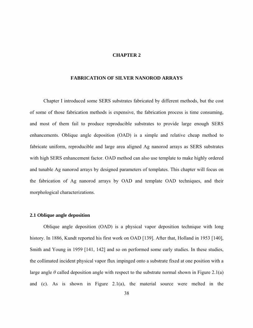
38
CHAPTER 2
FABRICATION OF SILVER NANOROD ARRAYS
Chapter I introduced some SERS substrates fabricated by different methods, but the cost
of some of those fabrication methods is expensive, the fabrication process is time consuming,
and most of them fail to produce reproducible substrates to provide large enough SERS
enhancements. Oblique angle deposition (OAD) is a simple and relative cheap method to
fabricate uniform, reproducible and large area aligned Ag nanorod arrays as SERS substrates
with high SERS enhancement factor. OAD method can also use template to make highly ordered
and tunable Ag nanorod arrays by designed parameters of templates. This chapter will focus on
the fabrication of Ag nanorod arrays by OAD and template OAD techniques, and their
morphological characterizations.
2.1 Oblique angle deposition
Oblique angle deposition (OAD) is a physical vapor deposition technique with long
history. In 1886, Kundt reported his first work on OAD [139]. After that, Holland in 1953 [140],
Smith and Young in 1959 [141, 142] and so on performed some early studies. In these studies,
the collimated incident physical vapor flux impinged onto a substrate fixed at one position with a
large angle θ called deposition angle with respect to the substrate normal shown in Figure 2.1(a)
and (c). As is shown in Figure 2.1(a), the material source were melted in the

39
crucible, the substrates were mounted on the substrate holder which connected a rotational motor.
Before the deposition, the substrates were rotated to a large angle relative to substrates normal.
They found that the tilting of substrates during the deposition could change the properties of the
film, which was probably due to the change of the film morphology. Till 1966, Nieuwenhuizen
et al reported the SEM images of these substrates and confirmed that the deposited Al films are
tilted columnar structures [143].
OAD film growth mechanism is mainly due to a so-called atomic shadowing effect and
adatom diffusion. As shown in Figure 2.1(b), during the initial stage of the deposition, the
impinging adatoms randomly condense onto a flat substrate, diffuse around the surface and form
individual separated island or nuclei. The size of nuclei is strongly dependent on the adatom
mobility of the material and the deposition conditions: the higher the adatom mobility, the larger
the nuclei. Since the incident vapor flux arrives at substrate at a very small angle, the taller
islands or nuclei act as the shadowing centers and block the atoms into the shadowed regions on
the substrate, thus there is no deposition in the shadowing region (Figure 2.1(c)). With the further
Motor
Substrate θ
(b)
(c)
Figure 2.1 (a) A schematic of oblique angle deposition; (b) and (c) Shadowing effect.
(a)
Source
θ β
Deposition angle
Tilting angle
Deposition angle

40
deposition (Figure 2.1(c)), the atoms can only land on top of the taller island or nuclei, which
makes taller island even taller, thus gives rise to the formation of columns growing in the
direction toward the incident deposition flux. In the meantime, deposition with high adatom
mobility materials can create larger diameter of isolated columns than the deposition with low
adatom mobility materials [144]. The formation of this kind of columnar structure requires not
only a large deposition angle to maintain atomic shadowing effect, but also low pressure (usually
~ 10-6 torr) and low temperature (room temperature). This is because at higher temperatures, the
surface diffusivity of adatoms increases and their diffusion length becomes large enough so that
the atoms are able to fill in the shadowed regions of the substrates [145].
Figure 2.2 shows the representative cross section SEM images of the evaporated films
deposited by OAD technique with different materials under different deposition conditions [5,
146-150]. These films are aligned columnar structures, and the columns are inclined away from
the substrate normal with an angle β. This kind of columnar structure is also called as nanorod
array, and the angle between the nanorod tilting direction and substrate surface normal is called
Figure 2.2 Cross section SEM images of nanorods of different material fabricated by OAD technique under different deposition conditions.
Cr: θ=80°, β=56° (Robbie et al, [146])
SiO: θ=86°, β=58° (Robbie et al, [146])
TiO2: θ=85°, β=52° (Kiema et al, [147])
Alq3: θ=85°, β=70° (Kiema et al, [147])
Cu: θ=75°, β=40° (Karabacak et al, [148])
Co/Cu: θ=85°, β=60° (Kar et al, [149])
Pt/Si: θ=86°, β=55° (He et al, [150)
Ag: θ=86°, β=72° (Driskell et al, [5])

41
as nanorod tilting angle β , which is shown in Figure 2.1(c). In most literatures, it is accepted that
there is a fixed relationship between the rod tilting angle β and the deposition angle θ for a
certain deposition conditions. Many scientists and researchers who worked on OAD tried to
understand and quantify this relationship, but it is actually complex and poorly understood. In
general, there are two main formula accepted in the literatures. The empirical “tangent rule” [143]
2/arctanθβ =t is more accurate when the deposition angle θ is smaller than 50°. As the
deposition angle becomes larger than 50°, it will give very poor explanation for the experimental
data. Trait et al [151] deduced a “cosine rule” ]2/)cos1arcsin[( θθβ −−=c based on geometrical
analysis which can give much better results for highly large deposition angle θ. But these
formulas can only give some qualitative predictions of column tilting angle β, they do not count
varied material and deposition conditions including background gas pressure and composition,
substrate and film temperature, and the energy and the distribution of the deposition flux.
Sometimes the measured tilting angle β is the average of the predicted value βt & βc. Therefore, it
is very hard to say which rule is “correct”, rather, experimental results tend to follow the trend
predicted by these formulas.
Because that the formation of columnar structure is the results of the competing effects of
surface diffusion and ballistic shadowing, both effects directly determine the diameter D and
density n of columns, parameters. Under the same deposition conditions, the ballistic shadowing
leads to the preferential growth of the tallest features on the surface, and smaller columns will
eventually fall into the shadowed regions cast by larger neighboring columns. This behavior
causes the extinction of the shadowed column since it will no longer receive any vapor flux. In
the mean time, due to the lateral diffusion, the columns will tend to fan out in a direction
perpendicular to the incident vapor direction since there is no mechanism restricting lateral
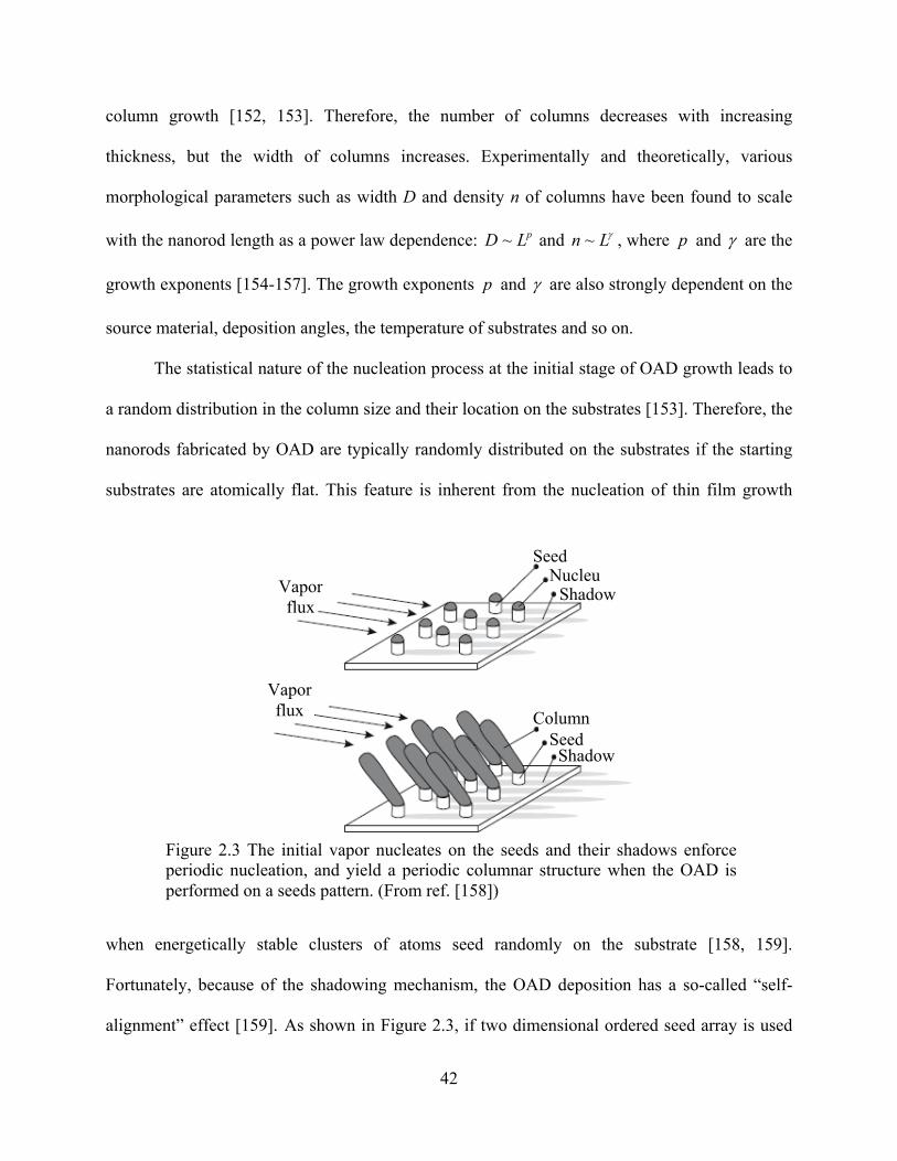
42
column growth [152, 153]. Therefore, the number of columns decreases with increasing
thickness, but the width of columns increases. Experimentally and theoretically, various
morphological parameters such as width D and density n of columns have been found to scale
with the nanorod length as a power law dependence: pLD ~ and γLn ~ , where p and γ are the
growth exponents [154-157]. The growth exponents p and γ are also strongly dependent on the
source material, deposition angles, the temperature of substrates and so on.
The statistical nature of the nucleation process at the initial stage of OAD growth leads to
a random distribution in the column size and their location on the substrates [153]. Therefore, the
nanorods fabricated by OAD are typically randomly distributed on the substrates if the starting
substrates are atomically flat. This feature is inherent from the nucleation of thin film growth
when energetically stable clusters of atoms seed randomly on the substrate [158, 159].
Fortunately, because of the shadowing mechanism, the OAD deposition has a so-called “self-
alignment” effect [159]. As shown in Figure 2.3, if two dimensional ordered seed array is used
Figure 2.3 The initial vapor nucleates on the seeds and their shadows enforce periodic nucleation, and yield a periodic columnar structure when the OAD is performed on a seeds pattern. (From ref. [158])
NucleuShadow
Seed
Seed Shadow
Column
Vapor flux
Vapor flux

43
as a template, the seeds can act as the shadowing centers. The deposition vapor would only
accumulate on the shadowing centers under the proper geometric deposition condition in OAD
and thus suppress the growth of random distributed nanorods. The separation, diameter and
density of the nanorods will only be determined by the structural designed parameters of the
designed template. This so-called template OAD has been used to fabricate three dimensional
photonic crystal structures recently [153, 160, 161].
To ensure that the initial vapor flux only grows onto the seeds, but not onto the bare
substrate between the seeds, the first consideration is to make that the shadow cast by one seed
only reaches to the edge of the nearest neighboring seeds along the direction of the incoming flux
for a given deposition angle. Thus the defined seeds pattern design is most important. As shown
in Figure 2.4, the edge-to-edge separation d between two neighbor seeds, the height h of seed
and deposition angle θ must follow the relation
)(tan 1 hdc−=≥ θθ , (2.1)
where cθ is called critical deposition angle shown in Figure 2.4. There is another requirement for
the diameter D of seed which must be close to the natural OAD column diameter, otherwise, the
significant column broadening and bifurcation will take place during the initial growth. Due to
the porous column structure fabricated by OAD, the mean density OADρ of a OAD film is always
less than the bulk density bulkρ of deposited material. Thus in the planar interface between a seed
layer and OAD column film, the seed layer must match the reduced film density, which requires
that the planar fill factor fA,seeds of the seed layer equals to the volume fill factor of the OAD
column film fV,OAD, where fA,seeds is defined as the fraction of a seed lattice unit cell (lattice period

44
dD +=Δ ) that is covered by actual seed material 2
2
,)2(
Δ=
Df seedsAπ , and fV,OAD is defined as
the fraction of a unit volume of the OAD column film that contains column film [161]
bulk
OADOADVseedsA ff
ρθρθθ )()()( ,, ≥= . (2.2)
Therefore, the template OAD requires both a specific lattice period dD +=Δ and a specific
volume fill factor fV,OAD.
2.2 Ag nanorod arrays fabrication by conventional OAD
There are many nanocolumnar structure films fabricated by OAD technique using
different material sources at different deposition angles. For examples, Brett group fabricated
nanocolumn of Cr, SiO, TiO2, Alq3 and so on [146, 147, 162]; Lu group fabricated nanocolumn
of Si, Rh, W, Co/Cu and so on [149, 152, 163]; Our group fabricated nanorods of Si, Pt/Si, TiO2,
WO3, Ti/Mg and so on [150, 164-166]. In 1986, Martinez et al used OAD to deposit Ag
columnar film for SERS detection [167, 168], however the SERS EF obtained from their
substrates was relative low and they also did not perform a systematic study on how the
columnar structures affect SERS enhancement. For SERS, Ag and Au are the two most
D
d
h
D d Δ
Flux θc
Figure 2.4 Schematics of seeds pattern

45
important materials for high SERS enhancements. We use Ag nanorod array fabricated by OAD
as SERS substrates. Here, we will give a detailed description of fabrication and morphological
characterization of Ag nanorod arrays fabricated by OAD techniques. In the later chapters, we
will perform a systematical study on the SERS characterizations and the SERS origin from Ag
nanorod array substrates.
2.2.1 Ag nanorod array fabricated on a flat substrate
The Ag nanorod arrays were deposited by a custom–designed electron-beam evaporation
system. Before the deposition, all 1 cm × 1 cm Si (100) wafers (or glass substrates) were cleaned
by a RCA-1 method (in 70°C solution of deionized (DI) water: hydrogen peroxide : ammonium
hydroxide = 5 : 1 : 1) for 20 minutes followed by DI water rinse. The clean substrates dried by
N2 were mounted onto a substrate holder, and the holder was put into the chamber of electron
beam evaporator. To obtain SERS substrates, the substrates were positioned directly toward the
incident vapor flux, and a 20 nm Ti adhere layer and a 500 nm Ag thin film were deposited onto
the cleaned Si wafers or glass substrates. The Ti and Ag were obtained from Kurt J. Lesker
company. Then the Ti/Ag film coated substrates were rotated to a large deposition angle with
respect to the deposition vapor, and finally a layer of Ag nanorod array was prepared by OAD
technique at different deposition angle θ = 78°, 80°, 82°, and 84°, respectively. During the
evaporation, the thickness of the metal deposited was monitored by a quartz crystal microbalance
(QCM) positioned at normal incidence to the vapor source; the Ti deposition rate was 0.1 nm/s;
the Ag film deposition rate was 0.3 nm/s, and the Ag nanorod array was prepared at a rate of
0.25 nm/s. Before the evaporation, the base pressure in the vacuum chamber was around 8.6 ×
10-7 Torr. For each deposition angle, 8 samples with different lengths were deposited. For

46
example, at θ = 84°, the QCM reading of Ag nanorod was l = 393 nm, 787 nm, 1180 nm, 1579
nm, 1968 nm, 2361 nm, 3148 nm and 3936 nm, respectively. The morphologies of as-deposited
samples were characterized by a field-emission scanning electron microscope (SEM) (FEI
Inspect F).
2.2.2 Morphological characterization of Ag nanorod arrays
Figure 2.5 show the top-view and cross-section SEM images of four representative Ag
nanorod arrays prepared at θ = 78°, 80°, 82°, and 84°, respectively. The QCM reading length l
for all four samples is nearly the same, 2310≈l ± 50 nm, and the measured nanorod length L =
1190 nm, 1160 nm, 1290 nm, and 1150 nm for θ = 78°, 80°, 82°, and 84°, respectively. In Figure
Figure 2.5 The top-view (up) and cross-section (down) SEM images of Ag nanorod arrays with length L ≈ 1200 nm prepared at θ = 78°, 80°, 82°, and 84°, respectively.
β= 61° β =64°
(a) θ = 78° (b) θ = 80°
β = 66° β = 67°
(c) θ = 82° (d) θ = 84°
1µm

47
2.5, all the four samples show tilted nanocoloumar structures with slightly different morphology:
for Ag nanorod samples deposited at smaller incident angles (θ = 78° and 80°), the Ag nanorods
connected together, forming a porous network structure as shown in both the top-view and cross-
section SEM images; while at large vapor incident angles (θ = 82° and 84°), the Ag nanorods
are well-separated. In order to obtain a better measurement of β , we plot the height h of
nanorods, i.e., the thickness of nanorod layer, versus the measured nanorod length L in Figure
2.6(a) for all the samples deposited at the same θ . All the data plotted in Figure 2.6(a) show a
linear relationship, and according to the definition of β , the slope of the plots
==ΔΔ= βcos/ Lhk 0.54, 0.49, 0.45, and 0.43 for θ = 78°, 80°, 82°, and 84°, respectively.
Thus the corresponding tilting angle β = 57 ± 2°, 61 ± 3°, 63 ± 3 °, and 65 ± 2 °, respectively.
The column tilting angles β is less than the deposition angle θ . Figure 2.6(b) plots Ag nanorod
tilting angle β as a function of deposition angle θ . With an increase of deposition angle θ , the
tilting angle β is shown to increase. This result is consistent with most of the reports for OAD.
Figure 2.6 (a) The plot of Ag nanorod height h versus the Ag nanorod length L for samples deposited at θ = 78°, 80°, 82°, and 84°, respectively ; (b) The Ag nanorod tilt angle β as a function of deposition angle θ.
(a)
0 300 600 900 1200 1500 1800 2100 24000
200
400
600
800
1000
1200
Hei
ght o
f Ag
Nan
orod
h (n
m)
Length of Ag Nanrod L (nm)
θ = 78o
θ = 80o
θ = 82o
θ = 84o
(b)
77 78 79 80 81 82 83 84 8554565860626466687072747678
β = (βt + βc)/2
βc = θ - arcsin[(1-cosθ)/2]
Experimental data
Ti
lting
Ang
le β
(D
egre
e)
Deposition Angle θ (Degree)
βt = atan[(tanθ)/2]

48
In the literatures, there are two empirical θβ − relationships proposed, the tangent rule
))tan(21arctan( θβ =t [169], or the cosine rule ]2/)cos1arcsin[( θθβ −−=c [151]. The two solid
curves in Figure 2.6(b) shows the predicted tilting angle at different θ for these two rules.
Unfortunately the measured β for Ag nanorods observes neither the tangent rule nor the cosine
rule, rather it falls in between tβ and cβ , and is close to the average value 2/)( ct βββ +≈ (the
dashed curve in Figure 2.6(b)).
From the SEM images, we also find that the diameter of the nanorod and the separation
between nanorods change with L and θ. Figure 2.7 shows the log-log plots of the diameter D
and the density n of Ag nanorods versus L for different θ. The diameter of the Ag nanorod D was
measured at the very growth end of the nanorod. With the increase of L, D becomes larger and
larger, while n becomes smaller and smaller. For example, when the length of Ag nanorods L =
1200 nm, the diameters of Ag nanorods are D = 170 ± 30 nm, 140 ± 20 nm, 130 ± 20 nm, and
120 ± 20 nm for θ = 78°, 80°, 82°, and 84°, respectively. In fact, both D and n follow power laws
(a) (b)
100 100040
80
120
160
200
240
D ~ Lp
θ = 78o, p = 0.30 ? 0.04 θ = 80o, p = 0.31 ? 0.03θ = 82o, p = 0.32 ? 0.03θ = 84o, p = 0.34 ? 0.02
Dia
met
er o
f Ag
Nan
orod
D (n
m)
Length of Ag Nanorod L (nm)100 1000
5
10
15
20
25
n ~ Lγ
θ = 78o, γ = -0.23 ? .03 θ = 80o, γ = -0.29 ? .04θ = 82o, γ = -0.31 ? .04θ = 84o, γ = -0.40 ? .05
Den
sity
n o
f Ag
Nan
orod
Length of Ag Nanorod L (nm)
Figure 2.7 The log-log plots of the diameter D (a) and the density n (b) of Ag nanorod versus the length L for various deposition angles θ.

49
with L: pLD ~ and γLn ~ [155-157], where p is the diameter growth exponent and is
determined as 34.030.0~ −p for different θ; and γ is the density growth exponent and is
determined to be )23.0()40.0(~ −−−γ for different θ . This exponent p is consistent with those
reported in the literature. Karabacak et al reported that the p was measurement to be ~ 0.28 –
0.34 for different materials, Co, Cu, Si, and W, deposited at θ = 85°, respectively [156]. Buzea et
al reported that the p value could be changed from 0.3 to 0.6 by varying θ from 75° to 89° for Si
deposition [155]. However, the exponent γ is very different in the literature. Smith et al reported
that 3.0~ −γ for TiO2 deposited at °= 86θ [154], while Zhou et al reported thatγ = -1.02 for Al
deposited at °= 84θ ; and for Ta deposited at °= 84θ , γ is more complex: with γ = -2.5 for the
Ta thickness smaller than 250 nm and γ = -0.5 for the thickness larger than 250 nm [170]. The
consistency of our reported p and those in the literatures show that p is almost independent of the
materials deposited, but is mainly determined by the shadowing effect [157], and at different θ, p
is slightly different; while for γ, it not only depends on the shadowing effect, but also strongly
relies on the deposited material.
2.3 Template Ag nanorod array fabrication and morphological characterization
The above Ag nanorod arrays are deposited onto the flat substrates, and the Ag nanorods
are distributed randomly on the substrates due to the random nucleation. Although the density,
tilting angle, and diameter of the Ag nanorods can be changed by varying the deposition angles
and deposition time, all these parameters are still very hard to control. Fortunately, we can apply
template OAD to fabricate ordered and uniformly arranged Ag nanorod arrays whose diameter,
separation and density could be determined by the parameters of template structure. Here, we

50
will explore the fabrication of semi-ordered Ag nanorod arrays by template OAD technique
combined with the electron beam lithography (EBL) technique by varying the diameter of Au
seed post array. The whole fabrication process of ordered Ag nanorod arrays includes two main
steps: one is the fabrication of seed patterns by EBL; another one is the fabrication of ordered Ag
nanorod array onto seed patterns by template OAD.
2.3.1 Fabrication of Au nanopost template array by EBL
EBL is a maskless lithographic process which uses a scanning focused electron beam to
directly write the designed pattern in the resist. EBL has been proven to be a powerful tool for
the fabrication of very small structure, and the resolution can be better than 10 nm [171]. Here,
we used EBL to fabricate nanopost array as template pattern. First, two dimensional Au/Ti nano-
post arrays in a square lattice was designed by AutoCAD drawing software. According to the
morphological parameters of the optimal Ag nanorod SERS substrates fabricated by the OAD
technique, i.e., a nanorod diameter ~100 nm and a separation ~179 nm [1, 37, 132, 135, 172-
174], three different nano-post array patterns with 50 µm×50 µm areas were designed with
diameter of each nano-post of 100 nm, 120 nm, and 140 nm, respectively, and a fixed edge-to-
edge separation 179 nm between the posts. Figure 2.8 shows the whole fabrication process of
template, and the fabrication was carried out by a JEOL JBX-9300FS EBL System at
Microelectronics Research Center in Georgia Institute of Technology. Before fabrication, silicon
substrates were cut into 1cm×1cm square and cleaned in piranha solution (5:1:1 volume mixture
of DI water, hydrogen peroxide (Becker, 30 wt.%), and ammonium hydroxide (Becker, 33
wt.%)), at a temperature of 75 ºC for 20 minutes, and were prebaked at 200 ºC for 5 minutes. The
clean substrates were spin-coated with the electron beam resist ZEP520A (Zeon Corp.) at 5000

51
rpm for 60 s to obtain a layer with a thickness of 300 nm, and were baked at 180 ºC for 2
minutes. Then, the ZEP520A coated substrates were exposed by electron beam at an acceleration
voltage 100 kV and a beam current 2 nA. The substrates with exposed resist were developed in
Amyl acetate for 2 minutes. A 20 nm Ti (99.995%, Lesker) and 80 nm Au (Williams Advanced
Material) film was evaporated subsequently on the patterned ZEP520A by electron beam
evaporator. During metallization using Au and Ti, the substrate was facing to the source directly.
Finally, the remained ZEP520A was dissolved in the remover 1165 (MicroChem Corp.), leaving
Au nano-post arrays on the substrates.
Figure 2.9 shows the typical SEM images of Au nano-post seed patterns with different
diameters. The diameters of Au nano-posts D are estimated to be D = 98 ± 8 nm, 119 ± 5 nm
Figure 2.8 sketch of Au nanopost array fabrication process by EBL
Si wafer cleaned in piranha (H2SO4:H2O2 = 4:1)
Prebake (200 ºC, 5 min) Spin coating ZEP520A 300 nm on Si (5000 rpm for 60 s)
Bake (180 ºC, 2 min) EBL exposure (100 kV, 2 nA, Dosage: 250 μC/cm2)
Patterned on ZEP520A
Metallization by E-beam evaporator (20 nm Ti + 80 nm Au on ZEP520A)
Lift off (in 1156 over night)
Au nanopost array on the Si
Development (Amyl acetate, 2 min)

52
and 143 ± 7 nm, respectively, the separation is d = 183 ± 6 nm, 179 ± 5 nm, and 175 ± 9 nm,
respectively, and the number density of Au nano-post along the horizontal direction is 3.6 µm-1,
3.3 µm-1 and 3.1 µm-1, respectively. From Figure 2.9, the top of Au nanopost is not a perfect
circle, there are several possible reasons: the incomplete liftoff may cause some metal residue
surround the nanoposts; the incomplete development, the old blanking amplifier employed
during e-beam exposure, the electron beam astigmatism during patterning, not proper focusing
and even not good skill of our SEM operator may also produce irregular shape of nanoposts.
2.3.1 Fabrication of semi-ordered Ag nanorod arrays by template OAD
After the seed patterns were prepared, Ag nanorod arrays were deposited onto Au nano-
post arrays by the OAD technique using a costumed electron beam evaporator. As shown in
Figure 2.1(a), the template substrates were mounted onto the substrate holder which tilted at an
angle of 86º between the substrate normal and the deposition direction. Recall equation (2.1), the
critical deposition angle )(tan 1 hdc−=θ . For all three templates, h = 100 nm, d = 179 nm, and
the critical angle °= 61cθ . At an incident angle θ larger than the critical angle, the shadowing of
the nearest neighbors can suppress random growth between the patterned nuclei [175]. Thus, a
500 nm
(a) (b) (c)
Figure 2.9 The top view SEM images of Au nano-post array seed patterns with the designed diameter: (a) D = 100 nm, (b) D = 120 nm and (c) D = 140 nm, respectively. The scale bars in the figures are the same.

53
regular Ag nanorod array could be fabricated when the evaporation flux is impinged onto the Au
nano-post array at a large incident angle 86º to the substrate surface normal. The detailed
fabrication procedure has been described in section 2.2. Since Ag deposition occurs almost at
room temperature, Au and Ag do not form an alloy. The thickness of the deposited Ag, recorded
by a quartz crystal microbalance that directly faced the deposition vapor, was 800 nm.
Figure 2.10 shows the typical SEM images of the Ag nanrod arrays on a blank Si substrate
and Au post arrays with different diameters. Ag nanorods on the blank Si substrate are randomly
distributed on the substrate surface (Figure 2.10(a)), while most of Ag nanorods on patterned
substrates only grow on the top of the Au posts (Figure 2.10(b) – (d)). Although each Ag
nanorod does not perfectly stay on each Au nano-post, the Ag nanorods still arrange more
uniformly and periodically on the Au nano-post arrays in the horizontal direction, perpendicular
1 µm
(b)
(c) (d)
(a)
Figure 2.10 The top view SEM images of Ag nanorods on (a) blank Si substrate (D =0), and on Au nano-post array seed patterns with the designed diameter, (b) D = 100 nm, (c) D = 120 nm and (d) D = 140 nm, respectively. The scale bars in the figures are the same.

54
to nanorod tilting direction and the vapor deposition direction. From the SEM images, the
diameters of Ag nanorod Dr on a flat substrate (assuming D = 0 nm for the blank substrate) and
Au nano-post substrates with D = 98 nm, 119 nm and 143 nm, can be estimated as Dr0 = 100 ±
20 nm, Dr100 = 130 ± 20 nm, Dr
120 = 150 ± 20 nm, and Dr140 = 160 ± 20 nm, respectively, the
edge-to-edge separation between the Ag nanorods is dr0 = 120 ± 20 nm, dr
100 = 150 ± 30 nm,
dr120 = 170 ± 30 nm, and dr
140 = 190 ± 20 nm, respectively, and the number density of Ag
nanorods along horizontal direction is 7.2 µm-1, 3.4 µm-1, 2.9 µm-1 and 2.6 µm-1, respectively.
Thus, both the diameter and separation of Ag nanorods becomes bigger with the increase of the
diameter of Au nano-post, which is different from the Au nano-post template. This increase in
diameter is consistent with the fan-out effect described in Figure 2.7(a). The number density of
patterned Ag nanorod along the horizontal direction is smaller than that of Au nano-posts, which
means some of the Ag nanorods are not on the top of the Au nano-posts. The deviation is 0.2 µm-
1, 0.4 µm-1, and 0.5 µm-1 for different Au nano-post seed patterns with different diameters D =
100 nm, 120 nm, and 140 nm, respectively, i.e., the larger the Au nano-post diameter, the larger
the deviation. These deviations come from multiple measurements at different locations for the
same substrates. This deposition result is different from our expectation for the template growth;
the possible reason is that the initial Au pattern area is too big, and the initial nucleation of Ag on
the Au post dominates the growth. This imposes an important need for a better control of the
template OAD technique in the future. A detailed study on template OAD growth of Ag nanorod
is needed in the future. We would need to take care of the following problems: (1) the template
design: would the current template design be adequate for template OAD growth? (2) the
understanding of Ag nanorod behavior; (3) the exploration of optimal growth conditions. As long
as we could fine tune both the diameter and the separation of nanorods and keep consistent

55
deposition uniformity, we could produce much better Ag nanorod SERS substrates. However,
the sum of the diameter and separation of the Ag nanorods follows a linear relationship with the
sum of diameter and separation of Au nano-posts, which is shown in Figure 2.11, i.e., the
patterned Au post arrays do act as a relatively good template.
2.4 Conclusions
In this chapter, large area aligned Ag nanorod arrays SERS substrates have been
fabricated by OAD technique. The diameter, density and tilting angle of Ag nanorod can be
determined by the deposition angle and time. Both the diameter and density follow power laws
with the length of Ag nanorods, with the exponents 34.0~30.0=p and 23.0~40.0 −−=γ for
various deposition angles. For Ag nanorods with the similar length, a larger deposition angle will
yield a smaller diameter. The tilting angle observes neither the tangent rule nor the cosine rule,
rather it falls in between tβ and cβ , 2/)( ct βββ +≈ . With the increase of deposition angles,
the tilting angle increases. In an attempt to produce more ordered and uniform Ag nanorod
270 280 290 300 310 320 330
260
280
300
320
340
360
380
Dr +
dr o
f Ag
Nan
orod
(nm
)
D + d of Au Nanopost (nm)
Figure 2.11 The sum of the diameter and separation of the Ag nanorods as a function of the sum of diameter and separation of Au nano-posts.

56
arrays, semi-ordered Ag nanorod arrays have been fabricated by template OAD method combing
EBL and OAD techniques. The diameter, separation and density of Ag nanorods can be adjusted
by the designed parameters of the template patterns.

57
CHAPTER 3
SERS FROM SILVER NANOROD ARRAYS: EXCITATION
CONFIGURATION DEPENDENCE
As mentioned in chapter 1 section 2, the magnitude of Raman electric field is
proportional to the magnitude of incident electric field, i.e., 0~~ gEEE LR αα . For most cases,
this incident E-field is also part of the primary field which is the sum of the incident field and
reflected fields by the nanoparticle and substrate. According to the electromagnetic behaviors in
the interface between the nanoparticle and substrate, one can directly change the incident power,
incident angle, polarization states and reflection of excitation light by nanoparticle and substrate
to change the magnitude of primary field and further change the Raman signal without the
consideration of LSPR. All these parameters are related to specific excitation configuration. In
this chapter, a series of experimental studies will be performed on the SERS dependences of
incident angle, polarization states and underlayer reflection of excitation light for Ag nanorod
arrays; in addition, a modified Greenler’s model will be proposed to give a theoretical
explanation for these SERS properties, and the theoretical calculations agree qualitatively with
the experimental results.
The Ag nanorod array substrates were prepared by OAD technique, and the fabrication
process has been illustrated in section 2 chapter 2. Here, a layer 20 nm Ti adhere layer and a
layer of 500 nm Ag thin film were first deposited onto the cleaned glass substrate (Gold Seal®

58
Cat No. 3010). Then a Ag nanorod array was deposited at a vapor incident angle of 86o. Typical
SEM images of the top and cross-sectional view of our standard Ag nanorod substrate are shown
in Figure 3.1(a) and (b). The tilting angle β of the nanorods was measured to be ~ 73o with
respect to substrate normal, the length was ~ 900 nm, the diameter was ~ 100 nm, the separation
was ~ 179 nm, and the density of Ag nanorod was ~13 rods/µm2 [151, 176, 177].
3.1 Incident angle dependence
Since the Ag nanorod array substrates used in this study are highly anisotropic (see, e.g.
Figure 3.1), different incident angles of excitation light could result in different Raman spectral
intensities, especially when the nanorod tilting plane of the Ag nanorods is parallel to the
incident plane, as shown in Figure 3.2. Therefore, we need to account for the effect of the laser
incident angle on the spectral intensities.
Figure 3.1 (a) and (b) are SEM images of the top and cross-sectional view of Ag nanorod array
(a)
(b)

59
3.1.1 SERS measurements
We used a fiber Raman system (HRC-10HT Raman Analyzer from Enwave Optronics
Inc.) for SERS characterizations. As shown in Figure 3.3, it consists of a diode laser, a
spectrometer, an integrated Raman probe head used for both excitation and collection, and
Glass substrate
β
ϕϕ
Positive incident angle
Negative incident angle
Ag film
Ag nanorod
Surface normal
Figure 3.2 Illustration of Ag nanorod array and incident configuration
Rotation
Laser Analyzer USB
Collecting Fiber
Exciting Fiber SERS Substrate
Laptop
Figure 3.3 The sketch of Enwave Raman probe and the setup of the incident angle dependence measurement.

60
separate delivery and collection fibers. The excitation source is a frequency stabilized, narrow
linewidth, near IR diode laser with a wavelength of λext = 785 nm. The excitation laser beam
coupled to a 100 µm fiber, is focused onto the substrate through the Raman probe head, and is
unpolarized at the sample. The focal length of the Raman probe is 6 mm, and the diameter of the
focal spot is 0.1 mm. The back scattered Raman signal from the substrate is also collected by the
same Raman probe head, and is coupled to a 200 µm collecting fiber, which delivers the signal to
the spectrometer equipped with a CCD detector. The Raman probe molecule used in this study
was trans-1,2-bis (4-pyridyl) ethene (BPE, Aldrich, 99.9+%). The BPE molecule gives SERS
peaks mainly at Δν = 1200 cm-1,1604 cm-1,and 1634 cm-1, and those bands of BPE can be
assigned to the C=C stretching mode, aromatic ring stretching mode and in-plane ring mode,
respectively. These three vibrational Raman modes are all aligned on the same molecular plane
[178]. Therefore, the SERS peak intensities of these three modes should follow the same trend.
(In fact, we have observed this trend, and will only discuss one particular vibrational mode, the
C=C stretching mode). A 10-6 M BPE solution was prepared by sequential dilution in methanol
(Aldrich, HPLC grade) and a 2 μL drop of BPE solution was placed onto the Ag nanorod
substrate where it formed a sample spot with a diameter of approximately 1.2 cm. The estimated
BPE molecular coverage on the nominal surface was 1.19×10⁻³ monolayers (assuming 7×10¹⁴
molecules/cm2 in a monolayer) [179]. Thus, approximately 1.39×10⁻¹⁴ moles of BPE were
excited in the laser spot.
For classification, we have assigned a positive incident angle when the incident direction
is facing the nanorod tilting direction as shown in Figure 3.2 (first quadrant in the incident
plane), while a negative incident angle is assigned when the laser strikes the surface on the other
side of the surface normal (second quadrant in the incident plane). All the SERS spectra reported

61
here were collected with an incident power ~ 30 mW, and a collection time of 10 seconds. SERS
spectra were collected from multiple spots on different samples in order to ensure the
reproducibility and accuracy of the measurements.
3.1.2 SERS of BPE collected at different incident angle
Figure 3.4 shows the representative SERS spectra of BPE on Ag nanorod arrays at the
different incident angles =ϕ -10°, 0°, +20°, +45° and +60°, respectively. All the spectra show
the characteristic Raman peaks of BPE at band =Δv 1200 cm-1, 1610 cm-1 and 1639 cm-1 [178].
These results demonstrate that even at very low BPE coverage, a Ag nanorod array prepared by
the OAD method can give very high signal-to-noise ratio (SNR) spectra.
Figure 3.4 also shows that the Raman peak intensities change with the incident angle ϕ .
From ϕ = -10o to ϕ = +45o, the peak intensity of each Raman band increases with an increase of
incident angle ϕ . Since these three vibrational Raman modes are all aligned on the same
Figure 3.4 Representative SERS spectra of BPE adsorbed on Ag nanorod substrate at different incident angles, ϕ = -10 o, 0o, 20 o, 45 o, and 60 o respectively. The peak intensity was strongest at around 45°.
1800 1700 1600 1500 1400 1300 1200 11000
1x10 4
2x10 4
3x10 4
4x10 4
5x10 4
60°
Raman Shift ( cm-1)
45°20°0°
-10°Ram
an In
tens
ity (c
ount
s)

62
molecular plane [178], the SERS peak intensities of these three modes should follow the same
trend. (In fact, we have observed this trend, and will only discuss one particular vibrational
mode, the C=C stretching mode). When the incident angle is larger than +45o, the Raman peak
intensity decreases, reaching a minimum value at +70°. This relationship is illustrated in Figure
3.5 by plotting the integrated intensity of the 1200 cm-1 band I1200 versus the incident angle ϕ .
The maximum SERS intensity is observed at about °+= 45ϕ , and is about 5 times the intensity
at °= 0ϕ (for most SERS measurement °= 0ϕ ). Note that the optimum angle 0ϕ is smaller than
the nanorod tilting angle β = 73o.Thus, the optimum experimental configuration to ensure
maximum SERS scattering response for this particular Ag nanorod arrays only is to put the
incident beam at °+= 450ϕ with respect to the substrate surface normal.
3.2 Underlayer effect
We also found that the film layers underneath the Ag nanorod array (underlayer) has a
significant effect on the SERS intensity. For our standard Ag nanorod array substrates, the
-20 0 20 40 60 800
2
4
6
8
10
I 1200
Incident Angle (degree)Figure 3.5 The integrated SERS intensity for the BPE band at 1200 cm-1 plotted as a function of the incoming laser incident angle.

63
underlayer is a layer of 500 nm Ag thin films on 20 nm Ti coated glasses. Therefore, the
underlayer of the above samples is 500 nm Ag thin film on 20 nm Ti coated glass. In order to
investigate the underlayer effect on SERS, four different underlayers are used: bare glass
substrate, bare Si wafer, 400 nm Ti on glass, and 400 nm Ag thin film on 20 nm Ti coated glass.
A ~ 900 nm Ag nanorod array deposited at 86° by OAD is prepared onto these four different
underlayers under the same deposition conditions as section 3.1.
3.2.1 Reflectance measurement for underlayer
After obtaining four different underlayers, the reflectance spectra from these underlayers
were measured using a UV-Vis 2450 spectrometer system with an integration sphere
(Shimadzu). Figure 3.6 show the representative reflectance spectra from different underlayers.
From Figure 3.6, the shapes of reflectance spectra are different for four different underlayers: in
wavelength range 300 nm – 850 nm, the maximum reflectance occur at λ = 350 nm, 368 nm, and
728 nm for glass, Si and Ti, while there is a broad reflectance peak appearing for Ag. In this
320 400 480 560 640 720 8000
20
40
60
80
100
120
400 nm Ag
400 nm Ti
Si
Ref
lect
ance
R %
Wavelength (nm)
Glass
Figure 3.6 The reflectance spectra of underlayers

64
wavelength range, the reflectance from Ag is the largest (~ 88%), while it is the smallest for
glass. At the excitation wavelength λext = 785 nm, the reflectance from bare glass substrate, Si
wafer, 400 nm Ti thin film on glass, and 400 nm Ag thin film on 20 nm Ti coated glass is 0.07,
0.3, 0.51, and 0.92, respectively.
3.2.2 SERS measurement and effect of underlayer reflectance
SERS from four different samples were obtained by HRC-10HT Raman Analyzer with
normal incident ( °= 0ϕ ). The Raman probe molecule was still BPE. A droplet (1µL) of BPE
with the concentration of 10-5 M was dispensed on the Ag nanorod array substrates with different
underlayers. The laser power was set at 44 mW, and the collection time was 10 s. Figure 3.7
shows the representative SERS spectra obtained from Ag nanorod arrays samples with different
underlayers. From Figure 3.7, Ag nanorod array with Ag thin film underlayer can produce an
extremely strong SERS intensity and the Raman peak intensity at band 1200 cm-1 AgI1200 ~ 27935
1100 1200 1300 1400 1500 1600 17000.0
5.0k
10.0k
15.0k
20.0k
25.0k
30.0k
Ram
an in
tens
ity (c
ount
s)
Raman shift (cm-1)
glass Si Ti Ag
Figure 3.7 The representative SERS spectra obtained from Ag nanorod arrays on different underlayers

65
counts, while Ag nanorod array on glass substrate gives a very weak SERS signal and the peak
intensity glassI1200 ~ 3784 counts. For four different underlayer SERS substrates, the
reflectance glassSiTiAg RRRR >>> , and the SERS peak intensity glassSiTiAg IIII 1200120012001200 >>> . Figure
3.8 is the plot of SERS peak intensity 1200I as a function of the reflectance from the underlayers.
Therefore, the SERS intensity increases monotonically with the reflectance from the underlayer
at excitation wavelength λext.
3.3 Polarization dependence
Recently, the polarization dependence of SERS has also been investigated for several
different nanostructural substrates such as nanoparticle dimmers [137], single nanoparticle [180],
regular arrays of nanospheriods [108], aligned nanowire bundles [138], Y-junction [181],
nanorod array [134], and single nanowire [182]. Due to the anisotropic structure of Ag nanorod
array, there is a unique polarization dependence of SERS.
0 20 40 60 80 1000.0
5.0k
10.0k
15.0k
20.0k
25.0k
30.0k
Ram
an p
eak
inte
nsity
I 1200
(cou
nts)
Reflectance from underlayer R %
Figure 3.8 The SERS peak intensity I1200 as a function of reflectance from underlayers

66
3.3.1 SERS spectra collection
In this investigation, the SERS spectra were recorded using a fiber-optic coupled,
confocal Raman microscope interfaced to a CCD-equipped spectrograph (Kaiser Optical
Systems Incorporated, Ann Arbor, MI). A fiber optic interfaced near IR diode laser 785 nm
(Invictus, Kaiser Optical) was used to provide the excitation light source. A Glan Thompson
prism broadband linear polarizer (Karl Lambrecht, Chicago. IL) and a broadband half-wave plate
(Karl Lambrecht) were placed to modify the incident beam. The polarizer directly was used to
linearly polarize the incoming excitation laser beam. The polarization direction of the incident
beam to SERS samples can be changed by rotating the half-wave plate. The polarization
dependent SERS spectra were acquired by rotating the half-wave plate by the increment of 15°
(one bar) which corresponds to 30° increment for polarization rotation, and the polarization angle
change from 0° to 360° with an increment of 30°. To simplify, we define p-polarization as the
direction of the incident electric field that is parallel to the major long axis of the nanorods
( °= 0ψ ) and s-polarization as the direction of the incident field that is perpendicular to the long
axis of the nanorods ( °= 90ψ ). Figure 3.9 shows a diagram of the definition of the polarization
Figure 3.9 Diagram of definition of incident light polarization
p (ψ = 0°)ψ
k
67
angle. In this study, the Raman probe molecule was also BPE. A droplet (2 μL) of BPE methanol
solution with concentration 10-5 M was placed onto the Ag nanorod array substrates. During the
spectra collection, the excitation light incidents normally ( °= 0ϕ ) onto the substrates, and
backscattering collection configuration was employed; the incident laser beam was focused onto
the sample through a 20 × microscope objective (N.A. = 0.40); the laser power on the sample
was ~ 14 mW and exposure time was 10 s.
3.3.2 Polarized SERS of BPE on Ag nanorod arrays
Figure 3.10 shows the polarization-dependent SERS spectra of BPE adsorbed on the Ag
nanorod array (the samples are the same as the samples used in section 3.4.1). The SERS peak
intensity (see 1200=Δv cm-1) in the figure increased with the increase of polarization angle ψ
from 0° to 90°. To better illustrate the anisotropic nature of the SERS polarization response, the
SERS peak intensity at band Δv = 1200 cm-1 was plotted as a function of polarization angle ψ in
a polar coordinate, as shown in Figure 3.11. From Figure 3.11, the SERS intensity excited by s-
1100 1200 1300 1400 1500 1600 17000
3000
6000
9000
12000
15000
18000
21000
24000
27000
ψ = 90o
ψ = 60o
ψ = 30o
ψ = 0o
Ram
an In
tens
ity (c
ount
s)
Raman Shift (cm-1)
Figure 3.10 Polarized SERS spectra of BPE on the Ag nanorod substrates

68
polarization is larger than that excited by p-polarization. In polarization angle ψ = 0° - 360°
range, the maximum intensity appeared at s-polarization (ψ = 90° or 270°), while the minimum
intensity occurred at p-polarization (ψ = 0° or 180°). In previous study, others in our group also
measured the polarized UV-Vis absorption spectra for this kind of aligned Ag nanorod arrays by
a UV-Vis-NIR double beam spectrophotometer (JASCO V-570) [134]. The spectrophotometer
was modified by putting two rotatable polarizers in the incident beams to obtain the polarized
absorption spectra. Figure 3.12(a) shows the absorbance representative spectra for different
polarized excitation light with polarization angle 0°, 4°, 9°, 24°, 34°, 54° and 90°. For p-
polarization (ψ = 0°), a broad absorption feature appears at Vis wavelengths above 400 nm.
When the polarization angle was rotated toward s-polarization (ψ = 90°), the absorbance of the
broad Vis contour steadily decreases, while a sharp UV peak emerges at 357 nm. This sharp peak
is attributed to the transverse Plasmon mode of the nanorod array. At excitation wavelength 785
nm, the absorbance dramatically decreases as the polarization rotates from p to s. Figure 3.12(b)
shows a polar plot of absorbance at excitation wavelength λ0 = 785 nm as a function of
0
30
6090
120
150
180
210
240270
300
330
0.0
4.0k
8.0k
12.0k
16.0k
20.0k
0.0
4.0k
8.0k
12.0k
16.0k
20.0k
I 1200
(cou
nts)
ψ
Figure 3.11 Polar plots of the SERS peak intensity at Raman band Δv = 1200 cm-1 of BPE as a function of polarization angle ψ.

69
polarization angle. Although more s-polarization light is absorbed by Ag nanorod array than p-
polarization light, due to the anisotropic absorbance by Ag nanorods layer, the larger SERS
intensity excited by s-polarization is larger than that excited by p-polarization collected from Ag
nanorod array substrate. For such results, we will give a theoretical explanation in chapter 5.
3.4 Modified Greenler’s model
From the above experimental studies, the SERS spectrum obtained from Ag nanorod array
substrates has the following three unique characteristics relative to excitation configuration: (1)
Incident angle dependence. The SERS intensity reaches the maximum value when the excitation
laser incident at an angle around 45º when the OAD deposition angle is 86º with a backscattering
collection configuration [183]. (2) Substrate reflectivity dependence. When a Ag nanorods array
is deposited onto various underlayers with different reflectance, the SERS signal increases with
the increase of the reflectance from the underlayers. (3) Polarization dependence. With a normal
0
30
6090
120
150
180
210
240270
300
330
0.00.61.21.82.43.0
0.00.61.21.82.43.0
Abs
orba
nce
ψ
300 600 9000.3
0.6
0.9
1.2
1.5
1.8
2.1
2.4
2.7
3.0
ψ = 90oψ = 54o
ψ = 34o
ψ = 24o
ψ = 9o
ψ = 4o
Abs
orba
nce
Wavelength (nm)
Incident angle ϕ = 0o
785 nm
ψ = 0o
Figure 3.12 (a) Representative absorbance spectra from Ag nanorod rod arrays excited by different polarized lights; (b) Polar plot of the relationship between the absorbance and polarization angles. (From ref. [134])

70
incidence excitation and the backscattering collection configuration, the s-polarization SERS
signal where the excitation E-field is perpendicular to nanorod long axis is higher than that of the
p-polarization [134]. Clearly all these three characteristics relate to the excitation configuration
for the same structure of the substrates. There is no existed theory to predict these behaviors for
nanorod array SERS substrates. However, a similar theory has been proposed to describe the
Raman spectrum of a molecule adsorbed on a flat surface. Greenler’s model is the first study on
the effects of the incident angles, the collecting angles and the polarization dependence of
Raman scattering by a molecule adsorbed on a planar surface through classical electrodynamics
[184]. Here we will propose a modified Greenler’s model to explain these SERS properties from
Ag nanorod arrays.
3.5.1 Greenler’s model
In early 1971, Greenler et al theoretically showed that there were an optimum incident
angle (70°) and collection angle (60°) for Raman scattering of molecules adsorbed on a Ag
planar surface based on classical electrodynamics, the excitation wavelength was 488 nm [184].
In this model, the Raman molecules are treated as oscillating dipoles. The primary field PE felt
by the molecule is the sum of the incident and reflected fields by the planar surface, and this
primary field induces an oscillating dipole in the molecule. The oscillating dipole can be
considered as a point source emitting Raman radiation. The sum of the directly emitted field and
the field suffering a single reflection from the surface is the secondary or scattered field RE . The
Raman intensity is proportional to the mean square of total scattered field 2>< RE . The detailed
description and derivations of Greenler’s model are shown in Appendix A.

71
3.5.2 The modified Greenler’s model
In Greenler’s model, the incident angle and incident light polarizations determine the
magnitude of the primary field. The strength and orientation of the induced dipole depend on the
mode symmetry of the molecule considered and its scattering cross section. The orientation of
the induced dipole also determines the variation in scattered intensity with observation angle.
This model gave some correct explanations for the Raman behavior of a molecule adsorbed on a
planar surface [185]. Thus, it naturally extends this model to SERS behavior of nanorod array
substrate. However, the nanorod substrate is not a planar substrate. Based on our experimental
results and conditions, we have made several further assumptions and proposed a modified
Greenler’s model to explain the dependence of incident angle, nanorod tilting angle, the
polarization and reflection of the substrate of the SERS intensity from BPE molecules adsorbed
onto Ag nanorods fabricated by the OAD method. For Raman scattering by a molecule adsorbed
on a planar surface, the behaviors of both the incident and scattering fields near this molecule
have been considered. Due to the high porosity and anisotropy of the Ag nanorod, we cannot
treat the substrate as a planar surface as in the standard Greenler’s model. Based on the
experimental geometry, we make the following assumptions.
(1) The surface of the nanorod can be simply treated as a planar surface by neglecting the
diffraction effect, and we only consider Raman scattering from a single nanorod. This is a very
crude assumption. The length of nanorods (~ 800 - 900 nm) is longer than the wavelength of the
excitation source (785 nm), while the diameter (~ 100 nm) is smaller than the wavelength. The
multiple scattering effects within adjacent nanorods need to be taken into consideration in the
future since the separation and diameter of the nanorods are much smaller than the wavelength of
the excitation source, and the Ag nanorod surface is rough [186].

72
(2) The BPE molecules are usually adsorbed on the sides and top of the nanorods, and are
also oriented perpendicular to the nanorod surface. According to Yang et al, the long axis of the
BPE molecule is always perpendicular to the adsorbed surface [178]. The gap between the Ag
nanorods is approximately 177 nm, which is much larger than the diameter of the BPE
molecules; and the nanorods have a large aspect ratio (~10). In the development of a scattering
model, the BPE molecule is treated as a dipole on the Ag nanorod surface, which is
perpendicular to the long axis of the nanorod.
(3) To be simple, the SERS effect of molecules on the top of Ag nanorods can be
neglected compared to the SERS intensity of the molecules on the side surface of Ag nanorods,
i.e. we do not consider the lightening-rod effect. Assume average SERS intensity as SERSI ,
SERS enhancement factor is G, and the intensity of primary field is pI , in terms of equations
(1.10) and (1.11), pSERS GII = . If the primary electric field PE can be decomposed as the field
⊥PE that is perpendicular to the nanorod long axis and the field ||PE that is parallel to the
nanorod long axis, the average SERS intensity can be written as 2||||||
2PPSERS EnGEnGI += ⊥⊥⊥
where ⊥n and ||n are the numbers of the molecules on the side and the top surface of nanorod
and ⊥G and ||G are the SERS enhancement factors at the directions perpendicular and parallel to
nanorod long axis respectively. If we assume the BPE molecules are uniformly adsorbed on the
Ag nanorod surface, for a single Ag nanorod, the ratio of BPE molecules on the side and the tip
of Ag nanorod surface is rl
SS
nn
top
side 2
||
==⊥ , where l is the length of the nanorod, and r is the
radius of the nanorod. According to our experiments, l ≈ 900 nm, r ≈ 50 nm, and 36||
=⊥
nn
. In

73
addition, from the UV-Vis polarized extinction spectra, the longitude mode plasmon peak of the
Ag nanorod array is around 1056 nm, and the transverse mode plasmon peak is located at about
357 nm [134], while the Raman excitation laser wavelength is 785 nm. This means that the
SERS observed in the experiments is not near the surface plasmon resonance frequency. Under
this condition, a rough numerical calculation using discrete dipole approximation (DDA) method
has shown that 1||
≈⊥
GG
. Thus the main contribution of the average SERS intensity can be
simplified as 2⊥⊥⊥≈ PSERS EnGI , i.e., the contribution to the SERS intensity of the molecules
adsorbed on the tip of Ag nanorod surface can be neglected compared with the contribution of
the molecules on the side surface of the Ag nanorod.
(4) In the experimental setup, a back scattering collecting configuration is employed,
which means that the exciting direction and the collecting directions have 180° phase difference.
Thus, in the proposed model, we also consider such a configuration.
Since any oscillating motion of the dipole can be decomposed into two orthogornal
motions which are parallel and perpendicular to the incident plane respectively, we can simply
consider two cases. The details of the model are depicted in Figure 3.13. Case I, the dipole is
parallel to the incident plane and case II, the dipole is perpendicular to the incident plane. For
case I, as shown in Figure 3.13(a), the incident light beam ① hits the molecule and reflects from
the surface of nanorod, another incident light beam ② hits the Ag thin film and reflects back to
the molecule. The incident beam ①, the reflected beam from the nanorod, and the reflection of
the beam ② all contribute to the primary field for the molecules on the nanorod, and excite the
molecules vibrating and radiating. One part of the radiation, or the scattered light ③ from the
molecule dipole directly goes to a detector, the other part of the scattered light ④ hits the

74
nanorod and is reflected by the surface of nanorod and then goes into the detector. For case II, as
shown in Figure 3.13(b), the incident light beam ⑤ hits the molecule, and the incident light
beam ⑥ hits the Ag thin film and reflected by the film, and then passes through the molecule. In
this case, the incident beam ⑤ and the reflection of beam ⑥ contribute to the primary field. The
scattered light ⑦ from the molecule dipole is directly collected by the detector, and no scattered
light reflecting from the nanorod enters the detector since the collection direction is
perpendicular to molecular vibrating direction in this case. The total Raman intensity is the sum
of the scattering intensities in case I and case II. In both cases, since the tilting of the nanorod
breaks the symmetry, if the excitation light incidents from right or left of the substrate surface
normal, ϕ is positive or negative. The nanorod tilting angle is β with respect to the normal of
substrates.
d β d
Ag thin film
x y
z
φ
Incident light
Indirect scattered
light
Direct scattered
light
Incident light
Direct scattered
light Incident light Reflected
light
φ
Reflected light
(a) Case I (b) Case II
Incident light
Ag thin film Glass substrate Glass substrate
Ag nanorod Ag nanorod
①
② ③
④
⑤
⑥ ⑦
Figure 3.13 A schematic illustration of the modified Greenler’s model. (a) Case I, the dipole is in the incident plane; (b) Case II, the dipole is perpendicular to the incident plane. All the induced dipoles are perpendicular to the nanorod.

75
3.5.2.1 The primary fields
Assuming that the fields isE , and ipE are s- and p- polarized components of the incident
light; the fields rsE , and rpE are s- and p- polarized components of the reflected light from the
Ag nanorod, and the fields rsE ′ and rpE ′ are the s- and p- polarized components of the reflected
light beams from the Ag thin film, respectively. The total phase shifts of the beam reflected by
the Ag nanorod surface compared with incident beam ① for the s- and p- polarized components
are sδ and pδ , rps δδ =, where rδ is the phase shift of beam ①. The phase shifts of the beam
reflected by Ag thin film compared with incident beam ① for the s- and p- polarized components
are s′δ and p′δ , drps δδδ += ′′′, where r′δ is the phase shift of beam ②, the phase shift due to the
optcal path difference between beam ① and ② is λπδ /2 Δ=d , and ϕ
ϕcos
)2cos1( +=Δ
d where d
is the vertical distance from the molecule to the Ag thin film. In our experiments, the length of
Ag nanorod is around 900 nm and the nanorod tilting angle is ~ °70 , so d varies from 0 to 308
nm. The reflected fields can be calculated by the Fresnel equations,
))sin~(/(cos))sin~((cos 21
222
21
222 iiiiisrss nnEEr ϕϕϕϕ −+−−== , (3.1)
))sin~(cos~/())sin~(cos~( 21
222
22
21
222
22 iiiiiprpp nnnnEEr ϕϕϕϕ −+−−== . (3.2)
Where iϕ is the incident angle with respect to the direction perpendicular to Ag nanorod,
ϕβπϕ +−=2i . The reflected fields from Ag thin film are given by the following equations:
))sin~(/(cos))sin~((cos 21
222
21
222 ϕϕϕϕ −+−−=′=′ nnEEr isrss , (3.3)

76
))sin~(cos~/())sin~(cos~( 21
222
22
21
222
22 ϕϕϕϕ −+−−=′=′ nnnnEEr iprpp , (3.4)
where sr and pr are the reflectivity of s- and p-polarized components by the Ag nanorod surface
and sr′ and pr ′ are the reflectivity of the s- and p-polarized components by the Ag thin film.
Let
2ss rR = ,
2
pp rR = , (3.5)
2ss rR ′=′ ,
2
pp rR ′=′ . (3.6)
The reflection phase shifts of s-polarization and p-polarization E-fields from the Ag nanorod and
the Ag thin film are,
])Re()Im([tan 1sss rr−=δ , ])Re()Im([tan 1
ppp rr−=δ , (3.7)
])Re()Im([tan 1sss rr ′′=′ −δ , ])Re()Im([tan 1
ppp rr ′′=′ −δ . (3.8)
The primary field at the nanorod surface is the sum of the incident and reflected fields from Ag
nanorod, and the reflected electric field from the Ag thin film, i.e. dirriP eEEEE δ′++=vvvv
. We set
the direction along the nanorods as the x -axis as shown in Figure 3.11(a), the direction
perpendicular to the incident plane and pointing inside as the y -axis, and the direction
perpendicular to the nanorod surface as z -axis. For case I, the components, xE , yE and zE of the
primary field in Cartesian coordinates can be written as
)cos(~)sin()sin( 22 βϕβϕβϕ +′−−+−−= rprpipx EnEEE , (3.9)
rsrsisy EnEEE ′++= 22
~ , (3.10)
)sin(~)cos()cos( 22 βϕβϕβϕ +′−−+−= rprpipz EnEEE . (3.11)
Thus, the intensity of the primary field for case I is

77
)],cos()2cos()sin(~2
)cos()2cos()sin(~2
cos)(sin2)(cos~
)(sin)([sin
21
212
2
212
2
221
242
2222
βϕδλπδβϕ
βϕλπδβϕ
δβϕβϕ
βϕβϕ
+−Δ+′−′+
+Δ+′−′−
−−+′+
−+−>>=<<
pppp
pp
ppp
pipx
RRn
Rn
RRn
REE
(3.12)
)],sin()2cos()cos(~2
)sin()2cos()cos(~2
cos)(cos2)(sin~
)(cos)([cos
21
212
2
212
2
221
242
2222
βϕδλπδβϕ
βϕλπδβϕ
δβϕβϕ
βϕβϕ
+−Δ+′−′+
+Δ+′−′+
−++′+
−+−>>=<<
pppp
pp
ppp
pipz
RRn
Rn
RRn
REE
(3.13)
).2cos(~2
)2cos(~2cos2
~1(
21
212
2
212
221
42
22
ssss
ssss
ssisy
RRn
RnR
RnREE
δλπδ
λπδδ
−Δ+′′+
Δ+′′++
′++>>=<<
(3.14)
And, the polarized primary intensity is
)],2cos(2sin~2
2sin)2cos(~2
)(2coscos2~1[
21
212
2
212
2
214
22
222
pppp
pp
ppppip
zxp
RRn
Rn
RRnRE
EEE
δλπδθ
βλπδ
βϕδ
−Δ+′′+
Δ+′′+
−+′++>=<
><+>>=<<
(3.15)
).2cos(~2
)2cos(~2cos2
~1(
21
212
2
212
221
42
2
22
ssss
ssss
ssis
ys
RRn
RnR
RnRE
EE
δλπδ
λπδδ
−Δ+′′+
Δ+′′++
′++>=<
>>=<<
(3.16)
78
In case II, because there are no reflections from Ag nanorod surface, 0== ps RR in equations
(4.15) and (4.16), the polarized primary intensity can be written as
],2sin)2cos(~2~1[ 212
24
22
222
βλπδ Δ+′′+′+>=<
><+>>=<<
pppip
zxp
RnRnE
EEE (3.17)
).2cos(~2~1( 212
24
22
22
Δ+′′+′+>=<
>>=<<
λπδ sssis
ys
RnRnE
EE (3.18)
3.5.2.2 The secondary fields
The radiation from the molecule dipole is the primary source for the secondary field. The
relationship between the scattering field and the incident field can be expressed as [187]
⎟⎟⎠
⎞⎜⎜⎝
⎛⎟⎟⎠
⎞⎜⎜⎝
⎛=⎟
⎟⎠
⎞⎜⎜⎝
⎛
incs
incp
Scas
Scap
E
E
E
E
_
_
_
_
1 00 sinφ
χ , (3.19)
βχ sin__ incpScap EE = , (3.20)
incsScas EE −= χ_ , (3.21)
where μχ 00 )exp( k
rrik
= , r is the distance between the dipole and observer (or the detector),
λπ2
0 =k , and μ is the molecular polarizability. Here, to be simplified, we set 1=χ , thus
ϕ22_
2_ sin>>=<< incpScap EE , and >>=<< 2
_2
_ incsScas EE .
In case I, the dipole is perpendicular to the nanorod and is also parallel to the incident
plane. We assume that dE is the directly scattered field from the dipole and rE is the field
scattered from the dipole toward the nanorod and then reflected toward the detector. The

79
components of the total Raman scattering fields EI recorded by the detector are EIx, EIy , and EIz,
respectively
ipd EE ϕ222 sin>>=<< , (3.22)
iridIx EEE ϕϕ coscos −−= , (3.23)
iridIZ EEE ϕϕ sinsin −−= , (3.24)
prdrdIZIxI EEEEEEE δcos222222 ++=+= , (3.25)
),cos21(sin
]2sin)2cos(~2
~1[
212
212
2
42
222
pppi
pp
pipipI
RR
Rn
RnEAEE
δϕ
βλπδ
++×
Δ+′′+
′+>=<×>>=<<
(3.26)
where,
),cos21(sin
]2sin)2cos(~2~1[
212
212
24
2
pppi
ppp
RR
RnRnA
δϕ
βλπδ
++×
Δ+′′+′+= (3.27)
For case II, the dipoles are not only perpendicular to the nanorod, but also perpendicular to the
incident plane. The total Raman scattering fields going into the detector is EII,
dII EE = , (3.28)
),2cos(~2~1( 212
24
22
2222
Δ+′′+′+>=<
×>>=<>=<>=<<
λπδ sssis
issdII
RnRnE
BEEEE (3.29)
where,
).2cos(~2~1( 212
24
2 Δ+′′+′+=λπδ sss RnRnB (3.30)
Therefore, considering both Case I and Case II, the total Raman scattering field totalRE − can be
written as

80
)].2cos(2~~1[
)(cos)cos21( )]2
cos(2sin~22sin)2cos(~2
)(2coscos2~1[
212
24
22
2
21
212
2212
2
214
22
22222
Δ+′′+′+><+
−++−Δ+
′′+Δ+′′+
−+′++>=<
×><+×>=<><+>>=<< −
λπδ
βϕδδλπ
δϕβλπδ
βϕδ
sssis
pppp
ppppp
ppppip
isipIIItotalR
RnRnE
RR
RRnRn
RRnRE
BEAEEEE
(3.31)
This equation reveals that the SERS intensity from nanorod array depends on the incident angle,
the nanorod tilting angle, the polarization of incident light, and the reflection of the substrate. In
the following, we will give a detailed discussion.
3.5.3 Results and discussions
3.5.3.1 The effect of incident and tilting angles
From equation (3.31), SERS intensity clearly depends on the incident angles and nanorod
tilting angles. For Case I, only the p-polarized light can induce dipole oscillation. Due to the
tilting of the nanorods, only dipoles on one side of the nanorods can be excited as shown in
Figure 3.11(a). For Case II, only the s-polarized incident light can induce dipole radiations.
When the incident light is unpolarized light, 2
222 ><
>=>=<< iipis
EEE . Assuming that the
nanorod tilting angle β is fixed, and Ramanη is the ratio of the total Raman scattering power to
incident light power called the relative Raman intensity, then, the relative Raman intensity Ramanη
excited by an unpolarized light can be expressed as

81
)]}.2cos(2~~1[
)(cos)cos21( )]2
cos(2sin~22sin)2cos(~2
)(2coscos2~1{[21
)(21
212
24
2
2
21
212
2212
2
214
2
22
Δ+′′+′++
−++−Δ+
′′+Δ+′′+
−+′++=
+=><>=< −
λπδ
βϕδδλπ
δϕβλπδ
βϕδ
η
sss
pppp
ppppp
pppp
itotalRRaman
RnRn
RR
RRnRn
RRnR
BAEE
(3.32)
From equation (3.32), the relationship between the relative Raman intensity Ramanη and the
incident angles can be calculated. In the calculation, we set the wavelength of incident light
785=λ nm, the index of refraction 1~1 =n for air, and the complex refractive index of Ag
in 242.503.0~2 += (for 785=λ nm) where 03.02 =n and 242.52 =k . Figure 3.14 plots the
relative Raman intensity Ramanη as a function of the incident angle ϕ for nanorod tilting angles
from 63º to 72 º. The Raman intensity increases with the incident angle initially, and then reaches
-30 -20 -10 0 10 20 30 40 50 60 70200
400
600
800
1000
1200
1400
1600
Rel
ativ
e R
aman
Inte
nsity
η Ram
an
Incident Angle θ (degree)
β =72 β =70 β =67 β =65 β =63
Figure 3.14 The relative Raman intensity Ramanη as a function of the incident angle θ calculated from the modified Greenler’s model for an Ag nanorod SERS substrate. The underlayer substrate is Ag, the excitation light is unpolarized, and the nanorod tiling angles are β = 63º, 65º, 67º, 70º, and 72º, respectively.

82
a maximum. With a further increase of the incident angle, the Raman intensity decreases. The
incident angle that results in the maximum Raman intensity is denoted as the optimal angle 0ϕ .
For example, in our experiments, the deposition angle was 86º and the tilting angle of the Ag
nanorods was °±= 43.71β , the optimal angle we measured was around °= 45oθ , and the
modified Greenler’s model give °= 470ϕ for °= 71β . The theoretical calculation is consistent
with the experimental results in the experimental error, which is shown in Figure 3.15. Figure
3.14 also shows that the maximum Raman intensity is almost the same for the Ag nanorod array
substrates with different nanorod tilting angles, and the curves shift to right with the increase of
the nanorod tilting angles, which means that the optimal incident angle ϕ increases with the
increase of nanorod tilting angles β . Figure 3.16 plots the relationship of 0ϕ versus β ; the
optimal angles 0ϕ change linearly from 40º to 49º when the nanorod tilting angles β change
from 63º to 72 º in equation (3.32).
-20 0 20 40 60 800
2
4
6
8
10
I 1200
Incident angle (degree)Figure 3.15 The SERS peak intensity as a function of the incident angle (scattered points), and the ratio of Raman scattering intensity to the incident light intensity calculated from the modified oscillating dipole model (solid curve).

83
3.5.3.2 The effect of the underlayer thin film
As demonstrated by the experiments, an Ag thin film layer underneath the Ag nanorod
array substrate plays an important role to enhance the Raman intensity. In equation (3.32), the
role of this thin film layer is reflected by sR′ and pR′ , the reflectivity from the underlayer film.
To see how different underlayers affect the Raman intensity, we consider four different
underlayers: (a) 400 nm Ag thin film coated on glass, (b) 400 nm Ti thin film coated on glass, (c)
bare Si wafer and bare glass substrate. For each of these underlayers, the refractive index is
inAg 24.503.0~ += , inTi 51.370.3~ += , inSi 03.013.4~ += , and 75.1~ =glassn at excitation wavelength
785 nm, respectively. At a fixed nanorod tilting angle °= 70β , the relative Raman intensity can
be calculated from equation (3.32). Figure 3.17 shows the relationship between the relative
Raman intensity Ramanη and the incident angles in four different cases. The excitation light is
unpolarized. If the excitation light is normally incident onto the substrates, i.e. °= 0ϕ , the
62 64 66 68 70 72 74
40
42
44
46
48
50
Opt
imal
Inci
dent
Ang
le ϕ
o(deg
ree)
Tilting Angle β (degree)
Figure 3.16 The optimal incident angle 0ϕ as a function of Ag nanorod tilting angle β under unpolarized excitation light.

84
corresponding reflectance for the four different underlayers, Ag, Ti, Si and glass, is 0.99, 0.57,
0.37, and 0.04, respectively. The relative Raman intensity Ramanη obtained from Ag nanorod
SERS substrates increases with the increase of reflectance from the underlayers, which is shown
Figure 3.17 The relative Raman intensity Ramanη as a function of incident angle ϕ for different underlayer thin films: Ag thin film; Ti thin film, Si wafe, and glass substrate The nanorod tilting angle is fixed, °= 70β .
-20 -10 0 10 20 30 40 50 60 70
0
200
400
600
800
1000
1200
1400Ag
Ti
Si
Rel
ativ
e R
aman
Inte
nsity
η
Incident angle ϕ (degree)
Glass
0 20 40 60 80 1000
5000
10000
15000
20000
25000
30000
0
200
400
600
800
1000
1200
1400
1600
Ram
an p
eak
inte
nsity
I 1200
(cou
nts)
Reflectance from underlayer R %
Experimental data R
elat
ive
Ram
an in
tens
ity η
Theoretical calculation
Figure 3.18 The SERS peak intensity as function of reflectance from underlayers

85
in Figure 3.18, and the theoretical calculation is qualitatively consistent with the experimental
results. Therefore, Ag thin film layer scientifically improves the Raman intensity.
3.5.3.3 The effect of the polarization of the excitation light
The Ag nanorod SERS substrate has anisotropic morphology, and is expected that the
enhancement factor should depend on the excitation polarization. A SERS polarization
dependence has been observed in our experiments [134]. To consider the effect of polarization
dependence, one can decompose any arbitrary state of incident polarized light into pEr
and sEr
.
The angle, ψ , is the polarization angle between the electric field direction and the p-polarization
E-field direction. So ψ222 cos>>=<< iip EE , ψ222 sin>>=<< iis EE . The Raman scattering
in case I can be only excited by the p-component of the E-field, i.e. >< 2IE corresponds to
><2
RpE and the scattering in case II can be only excited by the s-component of the E-field, i.e.
>< 2IIE corresponds to ><
2RsE . Thus, for the polarized incident light with polarization angle
ψ , the relative Raman intensity Ramanη in equation (3.32) becomes
)],2cos(~2 1[sin
)(cos)cos21)](2cos(
2sin~22sin)2cos(~2
)(2coscos2~1[cos
sincos
212
22
2
21
212
2212
2
214
22
22
Δ+′′+′++
−++−Δ+′
′+Δ+′′+
−+′++=
+=
λπδψ
βϕδδλπδ
ϕβλπδ
βϕδψ
ψψη
sss
ppppp
pppp
pppp
Raman
RnR
RR
RRnRn
RRnR
BA
(3.33)
where A and B are defined by equations (3.27) and (3.30), respectively. Figure 3.19 shows the
polarization angle ψ dependence of relative SERS intensity from the Ag nanorod substrate at

86
different incident angles obtained from equation (3.33). In the calculations, the layer underneath
is a Ag thin film with in 242.503.0~2 += , and the incident angle is taken from °0 to °75 with
°15 increment. At different incident angles, the shapes of the polarization dependent SERS
intensity are different. If the incident angles are smaller than °15 , the maximum SERS intensity
occurs at polarization angle of °= 90ψ and °= 270ψ , which means most of the Raman
scattering intensities observed are excited by the s-polarized component of the E-field, i.e., the
molecules shown in Case II in Figure 3.13(b). This is consistent with our experimental
observation at °= 0ϕ [134]. If the incident angle is larger than 15o, the SERS intensity reaches
the maximum at polarization angles of °= 0ψ and °= 180ψ , which means most of the Raman
0
30
6090
120
150
180
210
240270
300
330
0
4
8
12
16
20
0
4
8
12
16
20
η Ram
an ϕ =750
ϕ =600
ϕ =450
ϕ =300
ϕ =150
ϕ =00
ψ
Figure 3.19 The polarization dependence SERS intensity at different incident angles °= 0ϕ (navy filled circles), 15o (black filled squares), 30o (blue triangles), 45o (green
pentagons), 60o (red stars), and 75o (orange diamonds), respectively. When the incident angles ϕ are smaller than 15o, the SERS intensity reaches a maximum at polarization angle of 90o, and 270 o. When the incident angles are bigger than 15o, the SERS intensity reaches a maximum at polarization angles of 0o and 180o.

87
scattering intensities collected are excited by the p-polarized component of the E-field, or the
molecules shown in Case I in Figure 3.13(a). Note that, for any incident angle, the SERS
intensities at the polarization angles of °= 90ψ and °= 270ψ are almost the same, since the
Raman scattering only results from case II, which is independent of ϕ . However, the SERS
intensity at °= 0ψ and °= 180ψ increases with the incident angle first, reaches a maximum at
°= 450ϕ , and then decreases, which is consistent with Figure 3.11.
3.5 Conclusions
In this chapter, the incident angle dependence, polarization dependence, and underlayer
effect of SERS from the Ag nanorod arrays have been experimentally investigated. To explain
the experimental results of these SERS properties, a modified Greenlner’s model has been
proposed. The results deduced from this simple model are qualitatively consistent with our
experimental observations: (1) The SERS intensity is closely related to the incident angle. There
is an optimal incident angle where the SERS intensity reaches its maximum, and this optimal
angle increases linearly with the nanorod tilting angle. For Ag nanorod array with ~900 nm
length fabricated at deposition angle 86°, the optimum incident angle is ~45°. (2) The reflection
from underlayer thin film has a significant effect on the SERS intensity. The higher the
reflectance is, the larger the SERS intensity is obtained. (3) The SERS intensity is polarization
dependent. For °<15ϕ , s-polarization excitation contribute more SERS intensity. For °≥15ϕ ,
p-polarization excitation dominate the SERS intensity. The agreement between the results
calculated by this model and measured from experiments demonstrates that, although this is a
crude model, it has captured these essential characteristics of the SERS for Ag nanorod array,
and can be used to guide further experimental development.

88
CHAPTER 4
SERS FROM SILVER NANOROD ARRAY: SUBSTRATES STRUCTRAL
PARAMETERS DEPENDENCE
In chapter 3, only some SERS properties relative to the excitation configurations from the
same structural Ag nanorod arrays have been investigated. According to the brief review of
SERS mechanism in chapter 1, it is well known that the SERS activity strongly depends on the
size, separation and structure of nanoparticle systems. To obtain optimum Ag nanorod array
SERS substrates, in this chapter, we will study the effect of nanostructural parameters of Ag
nanorod arrays on SERS effect such as length dependence, diameter and separation dependence
of Ag nanorod arrays.
4.1 Length dependence of SERS from Ag nanorod array
Both Chaney et al and Driskell et al in our group found that the SERS enhancement factor
(EF) is strongly dependent on the length of Ag nanorods prepared at θ = 86°, and the optimum
SERS substrate is with L ≈ 900 nm [37, 132]. Here, we will systematically study the length
dependence of SERS for Ag nanorod arrays deposited at various deposition angles θ = 78°, 80°,
82°, and 84°. The detailed fabrication and morphological characterization of all Ag nanorod
array samples have been described in section 2.2. There are total four sample groups of Ag
89
nanorod arrays deposited at different deposition angles θ = 78°, 80°, 82°, and 84°, respectively.
Each group deposited at one deposition angle has 8 samples with different length of Ag nanorods.
4.1.1 Optical properties of Ag nanorod arrays
All SERS related studies have shown that the SERS activity of nanostructured films
strongly depends on the optical properties of the structures. We have demonstrated that the
absorbance spectra from Ag nanorod arrays on glass substrates is dependent on the length of Ag
nanorods [133]. Thus, it is very important to characterize the optical properties of our samples,
especially their optical absorbance properties. For our samples, the substrate is Si and there is a
500 nm thick Ag film deposited between Ag nanorods and Si wafer, therefore one can only
characterize the optical reflectance R of the samples. Their reflectance spectra were measured by
a UV-Vis 2450 spectrometer system with an integration sphere (Shimadzu). Figure 4.1(a) shows
reflectance spectra from Ag nanorod array substrates with different Ag nanorod length L
prepared at °= 84θ . For different L, the shapes of reflectance spectra are quite similar: they all
have an around constant R in near IR region. However, the absolute value of R at different
wavelength fluctuates with L, and more or less follows a similar trend. Figure 4.1(b) plots the
reflectance R at 785=λ nm as a function of L: the R first decreases with the increase of L,
reaches a minimum at L ≈ 1200 nm, then it increases with the further increase of L. In fact, for
the reflectance R at near IR region, it can be treated as a transmission through the Ag nanorod
array layer after the incident light was absorbed twice by Ag nanorod array since the reflectance
of 500nm-Ag film is ~ 1 at λ > 400 nm, which is shown in Figure 4.2. The reflection can be
expressed approximately as
aheR 2−= , (4.1)

90
where a is the effective absorbance coefficient under the assumption that for each sample the
Figure 4.1 (a) The reflectance spectra of Ag nanorod arrays with different length L deposited at θ = 84; (b) the reflectance R and absorbance A at λ = 785 nm as a function of nanorod length L; and (c) the spectra of the effective absorbance coefficient α for Ag nanorod arrays with different lengths deposited at θ = 84°.
200 300 400 500 600 700 800
0
10
20
30
40
50
60
70
80
Ref
lect
ance
R %
Wavelength λ (nm)
L = 170 nm L = 410 nm L = 590 nm L = 760 nm L = 890 nm L = 1150 nm L = 1590 nm L = 1970 nm
(a) θ = 84°
(c) θ = 84o
200 300 400 500 600 700 800 9000.0
2.0x10⁶
4.0x10⁶
6.0x10⁶
8.0x10⁶
1.0x10⁷
1.2x10⁷
Abs
orba
nce
coef
ficie
ncey
a
Wavelength λ (nm)
L = 170 nm L = 410 nm L = 590 nm L = 760 nm L = 890 nm L = 1150 nm L = 1590 nm L = 1970 nm
(b) θ = 84°
0 500 1000 1500 200045
50
55
60
65
70
0.16
0.20
0.24
0.28
0.32 Reflectance
Ref
lect
ance
R a
t 785
nm
%
Length of Ag Nanorod L (nm)
Abs
orba
nce
A
Absorbance
h dx
o x
α I0
I(h-x) x
y
Excitation beam Ag nanorod array
Ag thin film Figure 4.2 The incident and transmission configurations for SERS signal detection for the Ag nanorod array SERS substrate. This sketch illustrates the coordinates to calculate the effective EF based on the phenomenological model.

91
absorbance coefficient a is a constant across the entire thickness of the Ag nanorod film and h is
the thickness of Ag nanorod layer. The absorbance A of the Ag nanorod arrays can be written as
)log(2 RahA −== . (4.2)
In Figure 4.1(b), the absorbance A at 785=λ nm is also plotted as a function of L: it first
increases with L, reaches a maximum at L ≈ 1200 nm, then decreases with the further increase of
L. Under above assumption, the spectra of the absorbance coefficient α from Ag nanorod arrays
can be calculated. Figure 4.1(c) shows the spectra of a for nanorods with different length L
prepared at °= 84θ : the α value decreases monotonically with length L, this is because with the
increase of L, the diameter D of the nanorod increases while the density n of the nanorods
decreases in a faster manner so that the overall porosity of the Ag nanorod array decreases with
length L, i.e., the Ag volume filling ratio increases. According to the effective medium theory,
the a value is expected to decrease monotonically.
For samples with similar length L (≈ 1200 nm) deposited at different deposition angle θ,
the reflectance spectra R shown in Figure 4.3(a) are strongly dependent on the deposition angles,
especially for the wavelength region >λ 500 nm, the R-θ follows a similar trend. Figure 4.3(b)
shows the relationship of R at 785=λ nm and the deposition angle for a fixed L ≈ 1200 nm: the
R decreases monotonically with deposition angle θ , and an opposite trend of the absorbance A is
also shown in Figure 4.3(b). This result is consistent with the morphology of Ag nanorod arrays
due to OAD: with the increase of θ, the shadowing effect will play a bigger role in the thin film
growth, and the nanorod film becomes more porous, thus the effective absorbance coefficient a
becomes smaller. For nanorod array samples with similar thickness (or length), the larger the
deposition angle, the more porous the film, the higher the reflectance and the less the absorbance
the absorbance of Ag nanorod arrays substrates.

92
4.1.2 SERS measurements and characterizations
For SERS characterizations, the Raman probe molecule EBP with a volume of 1 µL and a
concentration of 10-5 M in methanol was also used. A 1 µL droplet of BPE methanol solution
was dispensed on the surface of Ag nanorod arrays. After the droplet was dried, the spreading
area was observed to be about 1 cm2 for all the substrates. The Raman spectra were recorded by
the HRC-10HT Raman Analyzer from Enwave Optronics Inc, with the excitation wavelength λext
= 785 nm, the excitation power 21 mW, the diameter of the laser spot was 0.1 mm, and the
collection time was 10 s. To obtain the SERS enhancement factor, normal Raman spectra were
measured from BPE methanol bulk solution with a concentration of 10-2 M contained in the
quartz rectangular cuvette with a path length of 1 mm.
The SERS spectra of BPE from Ag nanorod substrates have been shown in Chapter 3 and
we will not show the spectra here. In order to quantitatively compare the SERS substrates, the
Figure 4.3 (a) The reflectance spectra of Ag nanorod arrays with a fixed length L= 1200 nm prepared at different deposition angles; and (b) the reflectance R and absorbance A at λ = 785 nm as a function of deposition angles θ.
300 400 500 600 700 800
0
10
20
30
40
50
60
70
80
R
efle
ctan
ce R
%
Wavelength λ (nm)
θ = 78o
θ = 80o
θ = 82o
θ = 84o
(a) L = 1200 nm
78 79 80 81 82 83 84
48
52
56
60
64
68
72
76
0.16
0.20
0.24
0.28
0.32
Reflectance
Ref
lect
aanc
e R
at 7
85 n
m (
%)
Deposition angle α (degree)
(b) L = 1200 nm
Abs
orba
nce
A
Absorbance

93
SERS peak at Δν = 1200 cm-1 (the C=C stretching mode) and the equation SERS EF RSERS
SERSR
ININ
=
were used to calculate the SERS enhancement factor (EF), where RN and RI are molecular
number and Raman intensity in normal Raman measurement, SERSN and SERSI are SERS
molecular number and intensity [188]. In our experiment, the molecular number excited in
normal Raman measurement was estimated as 131089.4 ×=RN , and the normal Raman peak
intensity at band Δν = 1200 cm-1 was 1241200 =RI counts. The molecular number excited in SERS
measurement was about the same for all the SERS substrates, 81089.4 ×=SERSN . Figure 4.4(a)
plots the calculated SERS EF as a function of nanorod length L for Ag nanorod samples prepared
at θ = 78°, 80°, 82° and 84°, respectively. For different deposition angles, the SERS EF also
shows strong length dependence with a similar trend: the EF increases first with L, reaches a
maximum at an optimum L, and then decreases with further increase of L. More specifically, for
Figure 4.4 (a) The SERS EF as a function of nanorod length L for samples deposited θ = 78°, 80°, 82°, and 84°, respectively; and (b) the SERS EF as a function of deposition angle θ at a fixed nanorod length L = 165 nm.
78 79 80 81 82 83 84104
105
106
107 (170 nm)
(161 nm)
(163 nm)
EF
Deposition Angle θ (degree)
(165 nm)
(b) (a)
0 500 1000 1500 2000 2500104
106
108
1010
θ = 78o
θ = 80o
θ = 82o
θ = 84o
EF
Length of Ag Nanrod L (nm)

94
θ = 78°, L < 200 nm, the EF is relatively low (~104). The EF reaches a maximum value of 8.7 ×
105 at L = 660 nm, and then decreases slightly, and then increases to 2.0×10⁶ at L = 2100 nm. For
θ = 80°, the EF-L relationship follows the same trend of that for θ = 78°. The EF reaches a
maximum value of 7.0 × 10⁶ at L = 600 nm and 9.8 × 10⁶ at L = 2100 nm. For θ = 82°, the
SERS EF reaches a maximum value of 2.4 × 10⁷ at L = 660 nm. For deposition angle θ = 84°,
the maximum SERS EF value is 7.2 × 10⁸ at L = 1100 nm. For all the samples, the SERS EF
obtained from samples prepared at the deposition angle θ = 84° is apparently much larger than
those deposited at θ = 78°, 80°, and 82°. To further illustrate this point, we have selected four
samples with a fixed length L (≈ 160 nm) but deposited at different deposition angle θ, and
plotted the SERS EF as a function of θ in Figure 4.4(b). Figure 4.4(b) shows that for nanorod
samples with similar length, the larger the deposition angle θ , the larger the SERS EF. More
specifically, as θ increases incrementally by 2°, the SERS EF almost increases one order of
magnitude. There are several possible reasons for such a trend. First, from morphological point
of view, at small deposition angle θ , the density of Ag nanorod is large, there will be a higher
probability for two adjacent nanorods to contact each other, which changes the SERS hot spot
distribution, i.e., the two adjacent connected nanostructures could result in low localized electric
fields, and thus cause a low SERS enhancement factor for Ag nanorod arrays deposited at
smaller deposition angles. As shown in Figure 2.5, some Ag nanorods are even stuck together at
smaller deposition angle. Another possible reason is that the diameters of Ag nanorods deposited
at larger angles are relatively smaller at a fixed length L, and the diameter D of Ag nanorod is
larger than 100 nm for L > 200 nm for most of the samples (Figure 2.7(a)). Mo et al [189] and
Du et al [190] reported that the optimum size of the Ag nanoparticles for SERS activity was
around 100 nm. When the size was smaller than 100 nm, the SERS signal increased with an
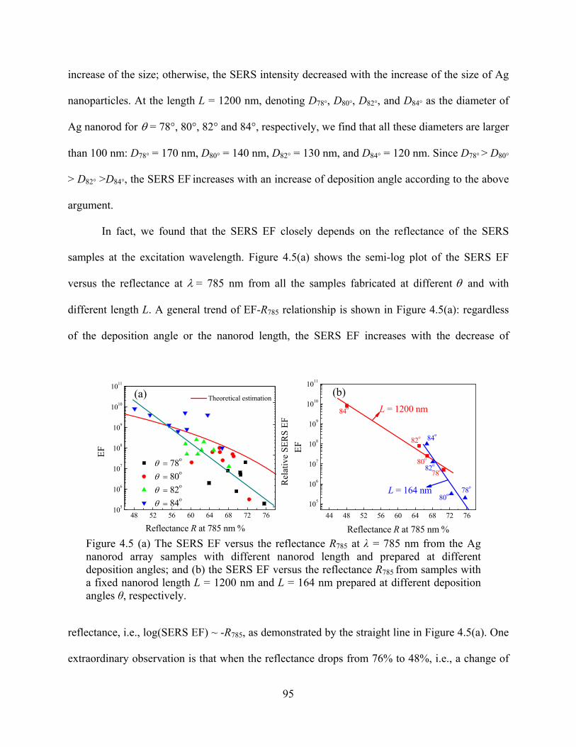
95
increase of the size; otherwise, the SERS intensity decreased with the increase of the size of Ag
nanoparticles. At the length L = 1200 nm, denoting D78°, D80°, D82°, and D84° as the diameter of
Ag nanorod for θ = 78°, 80°, 82° and 84°, respectively, we find that all these diameters are larger
than 100 nm: D78° = 170 nm, D80° = 140 nm, D82° = 130 nm, and D84° = 120 nm. Since D78° > D80°
> D82° >D84°, the SERS EF increases with an increase of deposition angle according to the above
argument.
In fact, we found that the SERS EF closely depends on the reflectance of the SERS
samples at the excitation wavelength. Figure 4.5(a) shows the semi-log plot of the SERS EF
versus the reflectance at λ = 785 nm from all the samples fabricated at different θ and with
different length L. A general trend of EF-R785 relationship is shown in Figure 4.5(a): regardless
of the deposition angle or the nanorod length, the SERS EF increases with the decrease of
reflectance, i.e., log(SERS EF) ~ -R785, as demonstrated by the straight line in Figure 4.5(a). One
extraordinary observation is that when the reflectance drops from 76% to 48%, i.e., a change of
(b)
Figure 4.5 (a) The SERS EF versus the reflectance R785 at λ = 785 nm from the Ag nanorod array samples with different nanorod length and prepared at different deposition angles; and (b) the SERS EF versus the reflectance R785 from samples with a fixed nanorod length L = 1200 nm and L = 164 nm prepared at different deposition angles θ, respectively.
44 48 52 56 60 64 68 72 76105
106
107
108
109
1010
1011
L = 164 nm 78o
80o
82o
84o
78o
80o
82o
84o
EF
Reflectance R at 785 nm %
L = 1200 nm(a) Theoretical estimation
Rel
ativ
e SE
RS
EF
48 52 56 60 64 68 72 76105
106
107
108
109
1010
1011
EF
Reflectance R at 785 nm %
θ = 78o
θ = 80o
θ = 82o
θ = 84o

96
28%, the SERS enhancement factor changes almost 5 orders of magnitude. Also, in Figure
4.5(a), the data can be categorized to four groups, each group corresponds to a specific
deposition angle θ . When the length L of Ag nanorods is set at a similar value, this relationship
can be even better illustrated, as shown in Figure 4.5(b). Figure 4.5(b) shows the SERS EF
versus R785 for fixed L = 1200 nm and L = 164 nm. For Ag nanorod arrays deposited at different
θ , the SERS EF apparently decreases with the increase of the reflectance at excitation
wavelength λ = 785 nm. Therefore, the SERS EF strongly depends on the reflectance from SERS
substrates. As we discussed above, the reflection is directly related to the absorbance by A = -ln
(R), which means for our SERS Ag nanorod array substrates, the larger the absorbance, the larger
the SERS EF.
4.1.3 Layer absorbance effect
The experimental results can be probably predicted from electromagnetic (EM) theory of
SERS. For example, Van Duyne’s group has performed a scanned wavelength SERS
measurement of Ag nanoparticle system, and they found that SERS intensity reached a
maximum when the excitation wavelength was close to the localized surface plasma resonant
(LSPR) wavelength, i.e., the maximum absorbance [98]. The work in Ref. [96] is different from
ours, since it focused on the effect of LSPR, and our Ag nanorod substrates do not show a
particular LSPR peak at λ0 = 785 nm. But phenomenologically, it is similar to our observation,
i.e., when the excitation laser wavelength is moved close to the LSPR wavelength, there will be a
higher extinction, and the nanostructure surfaces could have a higher local electric field
distribution, thus the structure will demonstrate the higher SERS EF. Theoretically, the total
absorbed power can be derived from the total fields on the surface of a small particle, hence the

97
absorption directly links to the local electric fields [191]. Thus, we believe that the layer
absorbance is closely related to the local electric field of the Ag nanorod substrates, and we
propose the following phenomenological model to qualitatively explain our experimental results.
We believe that the main SERS mechanism for Ag nanorod array substrates is
electromagnetic enhancement. For low frequency SERS band, the SERS EF is proportional to
the fourth power of local electric field LE , 4LEEF . According to above discussion, assuming
that the LE of nanorod array in a specific thickness x is directly proportional to the absorbed
power )(2 xaIEL ∝ , the SERS EF 22 )()( xIaxEF . Here we treat that the Ag nanorod array with
thickness h has a constant effective absorbance coefficient a , as shown in Figure 4.2, and I(x) is
the excitation intensity at the thickness x. Assuming that the SERS probe molecules are
uniformly distributed in the Ag nanorod layer, and the surface coverage of the probe molecules
for different samples with different length L and deposition angle θ is almost the same, then
total SERS EF can be expressed as
dxeeaIEF xhah xha )(
0
2)(0 )( −−−−∫ . (4.3)
The additional term )( xhae −− in the integration is added since the SERS signal excited at the
infinitesimal dx layer should experience absorbance by the Ag nanorods above this dx layer in
order to reach to the Raman detector. This consideration is due to our recent experimental and
theoretical findings regarding the importance of layer absorbance and anisotropic absorbance for
Ag nanorod substrates [130, 192]. After integration, the equation (4.3) gives us
aheEF 31 −−∝ , (4.4)
or according equation (4.1),
23
1 REF −∝ . (4.5)

98
Since 0 < R < 1, our model predicts that EF increases with the decrease of R, which qualitatively
agrees with the experimental results. In Figure 4.4(a), the rescaled function )1( 23
RCEF −= is
plotted together with the experimental data, where C is a constant. The predicted data follow the
experimental trend very well. However, since this phenomenological model does not consider
the specific local electric field distribution generated by the specific morphology, it cannot
predict the exact EF values and the detailed trend. To be more quantitative, one has to consider
the contributions from the details of the nanorod arrays, such as the randomness in nanorod
distribution, the irregularity, shape and size distribution of nanorods, the tilting angle and
specific length, etc. Only a sophisticated numerical calculation based on classic EM theory could
potentially provide such an answer. Nevertheless, our assumption based on the link between the
local electric field and absorbance does provide a qualitative view on the potential SERS
mechanism of the Ag nanorod array substrates, and further consideration could include this
finding.
4.2 Diameter and separation dependence of SERS from template Ag nanorod arrays
4.2.1 SERS spectra measurement
To study the SERS activity for both Au nano-post arrays and patterned Ag nanorod
arrays, we also applied a Raman probe molecule BPE. Figure 4.6 shows this experimental
design. First, a 1 μL droplet of 10-4 M BPE methanol solution was dispensed onto the Au nano-
post array, and the SERS spectrum was measured (Case I) (Figure 4.6(a)). After the Ag nanorod
array was deposited onto the BPE-coated Au nano-post array pattern prepared in Case I by OAD,
SERS spectra were obtained again at the patterned locations (Case II) (Figure 4.6(b)). We
assume that during Ag nanorod fabrication in Case II, the BPE molecules are not mobile, and

99
they only stay on the Si substrates or Au posts since the deposition temperature was lower than
40℃ [130]. Finally, after the SERS spectra were obtained for the Case II, an additional 1 μL
drop of 10-5 M BPE was dispensed on the top of the same location as in Case I, and SERS
spectra were again recorded (Case III) ((Figure 4.6(c))). All the SERS spectra were acquired by a
Renishaw Raman microscope system and a 50× magnification objective in back scattering
configuration under the same collection condition. During the SERS measurements, the
excitation wavelength was 785 nm, the excitation power was 1 mW, and the integration time was
10 seconds.
4.2.3 Diameter and separation dependence of SERS
Since we were not able to measure the reflection spectra for such small SERS substrates
(50 µm×50 µm), we instead measured the absorbance spectrum for a Ag nanorod array with the
(a) Case I BPE Molecules
Au nano-post
Ag nanorod (b) Case II
(c) Case III
Figure 4.6 Sketches of three different configurations for the SERS experiments, (a) Case I, a 1 μL drop of 10-4 M concentration of BPE is spread on Au nano-post array patterns; (b) Case II, Ag nanorods are deposited onto the samples from Case I; (c) Case III, a 1 μL drop of 10-5 M concentration of BPE is placed onto the samples from case II.

100
same length deposited on a glass substrate under the same conditions as shown in Figure 4.7. The
absorbance maximum appears at around λ ≈ 400 nm, and at near IR wavelength, i.e., λ = 785
nm laser excitation, there is no apparent local plasmon resonant (LSPR) peak. Thus the resulting
SERS signal is not due to excitation at LSPR wavelength. Figure 4.8 shows the normalized
SERS spectra by available surface area obtained from the Au nano-post arrays and patterned Ag
nanorod arrays in three Cases I, II and III. The peak intensity from the Au nano-post arrays were
too weak to observe as shown in Figure 4.8(a). This means that the Au nano-post arrays with a
height of 100 nm and different diameters (100 ~ 140 nm) are not activity SERS substrates under
400 500 600 700 800 900 1000 1100 12000.05
0.10
0.15
0.20
0.25
0.30
0.35
0.40
0.45
Abs
orba
nce
Wavelength / nm
Figure 4.7 The absorbance spectra of 800 nm Ag nanorod on the glass substrate
Figure 4.8 (a), (b) and (c) show the representative SERS spectra obtained from different patterned substrates for Case I, Case II, and Case III, respectively.
(a) (c)
1200 1300 1400 1500 1600 1700
200
400
600
800
1000
Ram
an In
tens
ity (c
ount
s) D =140 nm
D =120 nm
D = 100 nm
Raman Shift (cm-1)1200 1300 1400 1500 1600 1700
0.0
8.0k
16.0k
24.0k
32.0k
40.0k
D = 140 nmD = 120 nmD = 100 nm
Ram
an In
tens
ity (c
ount
s)
I 140III
I 120III
I 100III
I 0III
Raman Shift (cm-1)
D = 0
1200 1300 1400 1500 1600 17000.0
2.0k
4.0k
6.0k
8.0k
I 140II
I 120II
I 100II
I 0II
Ram
an In
tens
ity (c
ount
s)
D = 0
D = 100 nm
D = 120 nm
D = 140 nm
Raman Shift (cm-1)
(b)

101
our SERS detection conditions for BPE. Kondo et al fabricated Au nanodots with 70 nm
diameter and 100 nm interval between nanodots and performed studies about SERS height
dependence of Au nano-post with non-resonant excitation wavelength 633 nm, they found that
there was an optimum Au post height (~ 60 nm) for SERS [32]. The SERS signal first increases
with the increase of the height of nano-post, then reached a maximum when the height was
around 60 nm. After that, the SERS intensity decreased with a further increase of height of the
nano-post. In our experiments, the 100 nm height of the nano-post may not be optimized for
SERS detection under our conditions. However, the baseline of Raman signals increased with the
increase of the diameter of the Au nano-post. This is probably due to the increase of the
fluorescent background with an increase of the size of the nano particles. Figure 4.8(b) and (c)
show the representative baseline subtracted SERS spectra obtained from patterned Ag nanorod
arrays in Case II and Case III. For both cases, significant SERS spectra were obtained for all the
substrates. We use III0, III
100, III120, and III
140 to denote the SERS peak intensity of BPE obtained
from Case II for D = 0, D =100 nm, D = 120 nm, and D = 140 nm Au nano-post array substrates,
and IIII0, IIII
100, IIII120, and IIII
140 denote the SERS peak intensity of BPE for corresponding
samples for Case III. For Case II, as shown in Figure 4.8(b), III0 > III
100 > III120 > III
140, i.e. the
SERS intensity increases with the decrease of the diameter of seeds Au nano-posts. For Case III,
as shown in Figure 4.8(c), we also obtain similar results: IIII0 > IIII
100 > IIII120 > IIII
140. Compared
in Figure 4.8(b) and (c), the SERS intensity from Case III is about 9 times than that from Case II,
while we only added 1/10 of concentration BPE in Case III. This is because most of the SERS
signal comes from the side surface of the Ag nanorod other than the bottom of Ag nanorod [130].
To compare the relative SERS contribution of the Au-Ag junction and the Ag nanorod array, we
have performed a detailed analysis which is presented as the supporting material. With the

102
increase of the diameter and separation of the Ag nanorods, the SERS intensity decreases. Since
the SERS signal in Case III contains the SERS signal in Case II, in the following discussion we
can just consider the SERS intensities in Case III. Figure 4.9(a) plots the Raman peak intensity
I1200 obtained from Case III at Δv = 1200 cm-1 as a function of the diameter Dr and separation dr
of the Ag nanorods, respectively. The SERS intensity almost decreases linearly with the increase
of the diameter Dr, and also follows a power law I1200 ~ dr-2.39 with the separation dr of Ag
nanorods. Figure 4.9(b) also plots the Raman peak intensity I1200 at Δv = 1200 cm-1 as a function
of the sum l of the diameter Dr and separation dr of the Au nano-post (l = Dr + dr), the SERS
intensity also decreases with l as a power law, I1200 ~ l-2.05. We obtained a similar rule from two
batches of substrates fabricated at the same conditions. Thus, the SERS intensity strongly
depends on the diameter and the separation of the Ag nanorods.
Until now, it is well known that the SERS electromagnetic mechanism enhancement
strongly depends on the nanoparticle’s size, separation, shape and cluster arrangement [29, 90,
91, 101, 189, 190]. Previous studies have illustrated that the SERS signal relies closely on the
Figure 4.9 (a) The Raman peak intensities at Δv = 1200 cm-1 I1200 as functions of the diameter Dr and and separation dr of Au nano-post for Case III, respectively, (b) The Raman peak intensities at Δv = 1200 cm-1 I1200 as a function of the sum l of Dr the diameter Dr and and separation dr of Au nano-post.
200 220 240 260 280 300 320 340 360 3806.0k
9.0k
12.0k
15.0k
18.0k
21.0k
24.0k
I1200 ~ l -2.05
Ag nanorod l = Dr + dr / nm
(a) (b)
80 100 120 140 160 180 2005.00k
7.50k
10.00k
12.50k
15.00k
17.50k
20.00k
22.50k
25.00k80 100 120 140 160 180 200
Diameter Dr of Ag Nanorod / nm
I1200 ~ dr -2.39
Ram
an P
eak
Inte
sity
I 1200
/ co
unts
Separation dr between Ag nanorod / nm

103
size of the nanoparticles [29, 189, 190]. Mo et al reported that the optimum size of Ag
nanoparticles for SERS was around 100 nm [189], and Du et al further conformed this result
[190]. When the size of the Ag particle was smaller than 100 nm, the SERS signal increased with
an increase in size of the Ag nanoparticles, otherwise, the SERS intensity decreased with the
increase of the size of the Ag nanoparticles [190]. For nanoparticles, the SERS intensity depends
on the LSPR [39]. If the excitation laser wavelength is close to the LSPR wavelength, one can
obtain the maximum SERS intensity. However, in our case, as shown in Figure 4.10, there is no
resonant peak at 785 nm for 800 nm Ag nanorod. Thus the physical reason for the nanoparticle
size dependence may not be appropriate for nanorods. In fact, there are only a few studies in the
literature regarding how the nanorod diameter affects the SERS intensity. Liao et al fabricated
250 ~ 1000 nm long vertical Au nanorods and studied the SERS diameter dependence. They
showed that the optimum diameter of Au nanorod for SERS was 66 nm. They also concluded
that the SERS signal varied very little with the increase of the rod length and most SERS signal
come from the top of rods [29]. Their SERS enhancement is probably caused by the transverse
plasmon mode of the Au nanorods since the excitation beam propagated along the nanorods. But
for the tilted parallel large Ag nanorod array fabricated by the OAD technique, we have found
that the SERS strongly depends on the length of nanorods. The SERS intensity can change 3 ~ 4
orders for different nanorod lengths [132]. We have also calculated the local electromagnetic
field and found that a larger field magnitude appears at the bottom and side surface of Ag
nanorods other than the top, and most of the SERS signal comes from side surface of Ag
nanorods [130, 192]. Therefore, the SERS mechanism is more complicated for the tilted parallel
Ag nanorod array compared to the vertical nanorods, and the plasmon mode excited along the
nanorods becomes important.[134] This demonstrates that the gap between the nanorods can

104
greatly influence the SERS intensity. In Liao’s experiment, they did not mention how the
separation between neighbor Au nanorods changed when they changed the pore size of the AAO
template, and we do believe that their rod-rod separation was changed, which happens to our
substrates as well. Due to the coupling effect, the separation between the Ag nanorods could also
play a crucial role for SERS enhancement. Theoretically and experimentally, it has also been
proven that when the separation between nanoparticles, dimmers, or nanoparticles and nanorods
decreases, the electromagnetic coupling effect rapidly increases, and the local electric field
between nanoparticles becomes larger [74, 91, 106, 193, 194]. Xu et al found that the coupling
effect causes strong SERS enhancement when the separation of two small nanopartilces was less
than 10 nm [194]. They also demonstrated that the coupling between a small nanoparticle and an
extra long nanowire could also produce large SERS enhancement [193]. Both Gunnarsson et al
and our group found that the coupling effect still existed for a large separation for a large
diameter nanoparticle and also gives a significant contribution to SERS [91, 126]. Gunnarsson et
al used the EBL technique to fabricate Au nanodots with 200 nm diameter and 30 nm height and
studied the SERS separation dependence. The separation between Au nanorods varied from 100
nm to 500 nm. They found the SERS enhancement in the gap decreased with an increase of
separation of the nanodots as a factor (D/d + 1)4, where D is the diameter of nanodots and d is
the edge-to-edge separation [126]. From Gunnarsson paper, we can use a power law, i.e., I ~ d -
1.16 to fit their data. Recently, we also used EBL to fabricate Au nano-posts with 100 nm diameter
and 60 nm height and studied the SERS separation dependence [91]. The separation varied from
60 nm to 235 nm with a 25 nm increment. Although we cannot use a power law to fit our
previous experimental data for SERS separation dependence, the SERS intensity still decreased
rapidly with the increase of the separation of the Au nano-posts [91]. For the titled parallel Ag

105
nanorod array fabricated in this experiment, the SERS intensity strongly depends on separation
between Ag nanorods, and it follows a power law, i. e., I1200 ~ dr-2.39. This is qualitatively
consistent with Gunnarsson’s and our previous experimental results. However, in the above
treatments, the diameter Dr and separation dr are treated as independent parameters. In fact, these
two parameters are entangled together to contribute to SERS in our experiments. The parameter l
= Dr + dr may give a better explanation. In Gunnasson’s and our previous studies, the SERS
intensity I also decreased with the increase of the sum l of diameter D and separation d between
nanoparticles. We could use a power law, i.e., I ~ l -2.39 to fit Gunnarsson’s data. For a Ag
nanorod array, the SERS intensity also decreases with an increase of l as a power law, i.e., I1200 ~
l -2.05. The exponent is much closer to that of the Gunnarsson’s results. Therefore, the SERS
intensity depends on the combined contribution of diameter and separation of the Ag nanorods.
4.3 Conclusions
In summary, the SERS intensity extremely depends on the structural parameters of Ag
nanorod array system. One can adjust SERS activity by changing the length, diameter and
separation of Ag nanorods. For Ag nanorod arrays fabricated by OAD technique, there exists an
optimum length for SERS activity. In nature, the SERS intensity is strongly dependent on the
absorbance of Ag nanorod array which is determined by the length of Ag nanorods and the
deposition angle. More excitation light is absorbed by Ag nanorod array, larger SERS signal can
be obtained from Ag nanorod array. Due to the coupling effect, the SERS intensity extremely
relies on the separation of nanoposts. With the decrease of separation, the SERS intensity rapidly
increases. Diameter is another important factor to affect SERS activity. For Ag nanorods, the
optimum diameter is ~100 nm. To further understand structural parameters dependence of SERS,

106
we also studied separation and shape dependence of SERS from Au regular arrays fabricated by
electron beam lithography. Appendix B shows the separation dependence of SERS from Au
nanopost arrays, and Appendix C shows the shape dependence of SERS from Au nanorod array
and nanocomb arrays.

107
CHAPTER 5
THE ORIGIN OF SERS FORM SILVER NANOROD ARRAY
Chapter 1 has introduced the fabrication of Ag nanorod arrays. Chapter 2 and chapter 3
performed a detailed SERS characterization for the SERS substrates and also gave some
explanations for them. Except these SERS characteristics, we have great interest in studies on
the origin of SERS from the Ag nanorod arrays. In general, the enormous enhancement of the
Raman scattering is believed to originate from the “hot spots” on the surface, i.e., the surface
locations with extremely high local electric field enhancements due to the specific nanoscale
topologies of the metal surfaces [72]. For example, the small gaps (on the order of a few
nanometers) between Au or Ag nanoparticle aggregates (dimmers, trimmers, or larger
aggregates), the two ends of Au or Ag nanorods, and the corners of triangular shaped Au or Ag
nanoparticles can all be viewed as “hot spots” [42, 43, 195, 196]. The “hot spots” is considered
as the dominant mechanism for the single molecule detection. Experimentally, “hot spots” can
be observed through Raman imaging or mapping [78-80]. For Ag nanorod array, do the most
SERS signals still come from the “hot spots”?
The standard Ag nanorod array is shown in Figure 5.1(a), with Ag nanorod of length ~
900 nm, diameter ~ 100 nm, and tilting angle ~ 73o, and it can routinely achieve a SERS
enhancement factor (EF) of > 108 for the Raman probe trans-1, 2-bis(4-pyridyl) ethene (BPE)
[37, 134, 172].

108
These substrates have a very good uniformity and reproducibility compared to other
SERS substrates and have been demonstrated to distinguish different viruses and different
strains of viruses [1, 132, 172]. The SERS spectra obtained from these Ag nanorod array
substrates can be influenced by the incident angle, the underlayer thin film and the polarization
of the excitation light [134, 135, 174]. Due to the relative complex structure, so far the SERS
mechanism from those Ag nanorod substrates is not clear, although a simple model has been
proposed by us to explain the incident angle dependence and polarization dependence [134, 135,
174]. Are these strong SERS enhancements coming from “hot spots”? How do the “hot spots”
distribute on the substrate? Which parts of the surfaces on the nanorods give the highest SERS
enhancement? The attempt to answer those questions could help us to further understand the
SERS mechanism of the Ag nanorod substrate. In this paper, we will show our first attempt to
understand those questions. We first use the three-dimensional finite-difference time-domain
method to numerically calculate the local electric field distribution of regular Ag nanorod array
surface and find the potential “hot spots”. Then we designed two sets of experiments to
investigate which surfaces of the nanorods give the highest SERS enhancement, and their
excitation polarization dependence. Finally, we propose that the anisotropic absorbance of the
Ag nanorod layer play a significant role in determination of the SERS enhancement for Ag
nanorod array substrates.
5.1 Electric field “hot spots”
Experimentally the observation of nanometer scale “hot spots” in Ag nanorod arrays has
proven difficult. However, it has proven to be relatively easy and accurate to find the
distribution of electric field “hot spots” through numerical calculations [72, 74]. We used the

109
three-dimensional finite-difference time-domain (3D-FDTD) method to calculate the local
electric field distribution of Ag nanorod array. The brief introduction to FDTD is shown in
Appendix D. The Ag nanorod model for the calculation is shown in Figure 5.1(b). The needle-
shaped Ag nanorods have a bottom diameter of 50 nm, a top diameter of 100 nm, a length of 900
nm, and are tilted at an angle of 71o with respect to the substrate surface normal. The center-to-
center separations between nanorods along the x-axis and y-axis are Lx = 863 nm and Ly = 177
nm, respectively. The supporting Ag film underneath the nanorods is 500 nm thick. These
structural parameters used in the FDTD calculations approximate the experimentally observed
nanostructure in our Ag nanorod arrays [37, 132, 134]. Two excitation wavelengths (λ = 785 nm
and λ = 633 nm) and two different polarization states (p-polarization incident E-field direction
parallel to x-axis, e.g. Figure 5.1(c)) and s-polarization incident E-field direction parallel to y-
axis, e.g. Figure 5.1(d)), were used in the FDTD calculations. The FDTD calculations were
carried out with 5-nm cells and 7 layers PML(perfectly matched layer) absorption boundary
x y
(b)
Lx
z
o
Ly
E k
E k
Hot spot (c)
(d)
0 20
(a)
Figure 5.1 (a) A SEM image of Ag nanorod array; (b) A diagram of the 3 × 3 Ag nanorod array model; (c) and (d) are the E-field distribution under p-polarization incidence in the xz plane and yz plane, respectively.

110
condition. The permittivity of Ag is given by the modified Debye
model,01
)(ˆωεσ
ωτεεεωε
iis ++
−+= ∞
∞ , where ε̂ is the complex relative permittivity, ω is the
angular frequency, 834.3=∞ε is the relative permittivity at infinite-frequency, 5.9530−=sε is
the relative permittivity at zero-frequency (static relative permittivity), s151035.7 −×=τ is the
relaxation time, and ms /10149.1 7×=σ is the conductivity [197].
Figure 5.1(b) shows the local E-field distributions ( ||/|| 0EElocal
vv) under p-polarization
excitation with λ = 785 nm. Under p-polarized excitation, “hot spots” are found located at the
corners between the bottom of the nanorods and Ag thin film, where the local E-fields are much
stronger than those around other locations on the nanorod. The relative magnitude of the E-field
at those “hot spots” is ~ 20. Under s-polarized excitation (Figure 5.1(c)), the electric fields along
the side surface of the nanorod are stronger than those on the other locations, while the
maximum magnitude of the E-field along the side of the Ag nanorod is ~2. The FDTD
calculations illustrated in Figure 1 produce two results: the maximum enhanced field strength
under s-polarization is much smaller than that under p-polarization, and the enhanced fields
under p-polarization produce “hot spots” for the nanorod at the corners of the bottom of the
nanorod and the underlying Ag thin film, i.e., the “hot spots” are buried under the Ag nanorods.
It would be quite interesting to know whether those “hot spots” can still play a dominate role in
SERS signal.
5.2 Experimental design to locate Raman probe molecules
In order to observe the SERS effect from different locations on the Ag nanorod
substrates, we have designed the following experiments as shown in Figure 5.2: First, a 500-nm

111
Ag thin film was deposited on a glass substrate. A 1 μL droplet of a Raman probe molecule,
trans-1, 2-bis (4-pyridyl) ethene (BPE, 10-4 M Aldrich, 99.9+%), was uniformly dispersed onto
the Ag thin film substrate, and the SERS spectrum was measured [Figure 5.2(a), Case I].
Subsequently, a Ag nanorod array, prepared by oblique angle deposition, was deposited onto the
BPE-coated Ag thin film substrate prepared in Case I, SERS spectra were then obtained without
the addition of any more BPE solution [Figure 5.2(b), Case II]. Finally, after SERS spectra were
obtained for the Case II sample, an additional 1 μL drop of 10-5 M BPE was dispensed on the
top of the same sample location as in Case I, and SERS spectra were again obtained [Figure
5.2(c), Case III]. The thin film and nanorod fabrication conditions in these experiments were
identical to those previously reported [37, 134, 172]. SERS spectra were acquired using a
Renishaw inVia Reflex Raman microscope system (Renishaw, Hoffman Estates, IL) at λ = 785
nm with 0.22 mW laser power, 20 s collection time, and 20× magnification objective. At λ =
633 nm, spectra were obtained using 0.56 mW laser power, 10 s collection time, and 5×
magnification objective. The λ = 633 nm beam is linearly polarized (extinction ratio > 500 : 1),
while the λ = 785 nm beam is elliptically polarized.
Figure 5.2 An illustration of the three different samples designed to illustrate the effect of “hot spots” on the SERS spectra of Ag nanorod arrays, (a) Case I. A 1 μL drop of 10-4 M BPE was put onto a Ag film; (b) Case II. Ag nanorods were deposited by oblique angle vapor deposition onto the samples in Case I; (c) Case III. A 1 μL drop of 10-5 M BPE was placed onto the sample in Case II.
(c) (a)
10-4 M BPE molecules
Glass substrate Ag thin film
(b)
Ag nanorod 10-5 M BPE molecules

112
5.3 The SERS Enhancement factor at different substrate locations
If the “hot spots” shown in Figure 5.1 play a dominant role in the mechanism of the SERS
response in Ag nanorod array substrates, the SERS intensities from Cases II and III should be
comparable, since the second droplet contains one tenth the concentration of the first and
spreads over a much higher surface area (nanorod compared to flat). Figure 5.3(a) shows the
representative BPE spectra obtained at λ = 785 nm for Cases I, II and III. The SERS signal for
Case I is too weak to observe, while a notable SERS intensity is observed for Case II. For case
III, however, a very strong SERS signal is shown that is approximately 10 times that of Case II.
Using the Raman peak intensity at 1200 cm-1, which corresponds to the C=C stretching
vibrational mode of BPE, to quantitatively analyze the spectra, the peak intensity IIII for Case III
was calculated to be 9 ± 2 times the intensity III for Case II. This demonstrates that the SERS
signal are enhanced significantly after applying 10-5 M BPE on the surfaces of Ag nanorods.
We have estimated the relative contribution of the locations to the SERS response. For
Case II, bbII GNI ∝ , and for Case III, )( ssbbIII GNGNI +∝ , where bN and sN are the number
of BPE molecules on the bottom and surfaces (side and top) of the Ag nanorods under the same
excitation beam size, bG and sG are the effective SERS enhancement factor on the bottom and
surfaces of the Ag nanorods, respectively. From morphological characterization, the area of the
Ag nanorod side walls is around 1 ~ 2 times the projected surface area of the Ag thin film.
Experimentally we observed that the area spread by a 1 μL droplet of BPE solution in Case II is
1.2 ~ 1.6 times that in Case I. Thus, one can estimate that 20~15/ ≈sb NN under the same laser
spot. The SERS intensity due to nanorod surfaces IIIIIR III −= , thus 8// ≈= bbssIIR GNGNII .
This predicts that 200~50/ ≈bs GG , i.e., the SERS enhancement factor on the surfaces of
nanorods is significantly larger than that from the bottom surfaces. Compared to the FDTD

113
calculations in Figure 5.1(c), we conclude that the main contribution of SERS of Ag nanorod
array is from the nanorod surfaces, and that the “hot spots” at the corners between the nanorods
and the Ag film play a less significant role, which is contrary to most SERS substrates.
5.4 Polarization dependence of SERS signals
The polarized SERS spectra also support such a conclusion. Figure 5.3(b) shows the
SERS spectra acquired at different polarizations under λ = 633 nm for Cases III and II. Under
both s- and p-polarizations, the SERS intensities obtained from Case III, sIIII and p
IIII , are much
stronger than those obtained from Case II, sIII and p
III . The Raman peak intensity ratios sII
sIII II /
and pII
pIII II / are 9 ± 2 and 8 ± 2, respectively, which is consistent with the ratio obtained at λ =
785 nm. In addition, the Raman peak intensity excited at s-polarization is always larger than that
excited at p-polarization for both Cases II and III. If we only consider the molecules added in
Case III, the polarization ratio 7.02.2)/()( ±=−− pII
pIII
sII
sIII IIII , and this ratio is consistent with
our previous observations [134].
(a) (b)
1200 1300 1400 1500 1600 1700
0
10k
20k
30k
40k
50k
Case ICase II
Case III
Ram
an In
tens
ity (c
ount
s)
Raman Shift (cm-1)
1200 1300 1400 1500 1600 17000
10k
20k
30k
40k
I pIII
I sII
I pIII
Ram
an In
tens
ity(c
ount
s)
Raman shift (counts)
I sIII
Figure 5.3 (a) The representative SERS spectra obtained from samples prepared in Case I, II and III;(b) The representative spectra obtained from different polarization excitation at 633 nm in Case II and Case III.

114
5.5 The layer absorbance model
If the SERS enhancement is caused only by the local field enhancement, for Case II,
bp
lbA
slbb AdsEEG
b
/)(21 44
+∝ ∫∫ , and for Case III, sA
pls
slss AdsEEG
s
/)(21 44
∫∫ +∝ , where slbE and
slsE are the local electric fields at the surface of the Ag thin film and the surfaces of the nanorods
under s-polarization excitation, plbE and p
lsE are the corresponding local electric fields under p-
polarization excitation, and bA and sA are the corresponding surface areas. The ratio bs GG / can
be directly estimated from the FDTD calculation, and we obtain bs GG / ≈ 0.8. This estimated
value is much smaller than the experimental value of 50 ~ 200. Also, the predicted polarization
intensity ratio for molecules added in Case III, 05.0/ ≈ps II , is inconsistent with the
experimental results.
However, if we consider that the BPE molecules are distributed in a depth, and the SERS
signals excited at the bottom of and inside the film have to propagate through a distance in the
film in order to reach the Raman detector, which means those SERS signals will be attenuated by
the absorbance and scattering of the effective layers above. Then, the effective absorbance of the
SERS signals by the Ag nanorod layer cannot be ignored. Also, considering the anisotropic
nature of the Ag nanorod arrays shown in Figure 5.1, the absorbance for s-polarization light and
p-polarization light is different [134], we can estimate that for Case II,
∫∫ +++∝ −−
b
sp
Ab
pylb
sylb
dpxlb
sxlb
db AdsEEeEEeG /)]|||(|)|||(|[
21 4444 αα , (5.1)
and for Case III,
∫∫∫ +++∝ −−
Ass
pyls
syls
zpxls
sxls
zd
s AdsEEeEEedzG sp /)]|||(|)|||(|[21 4444
0
αα , (5.2)
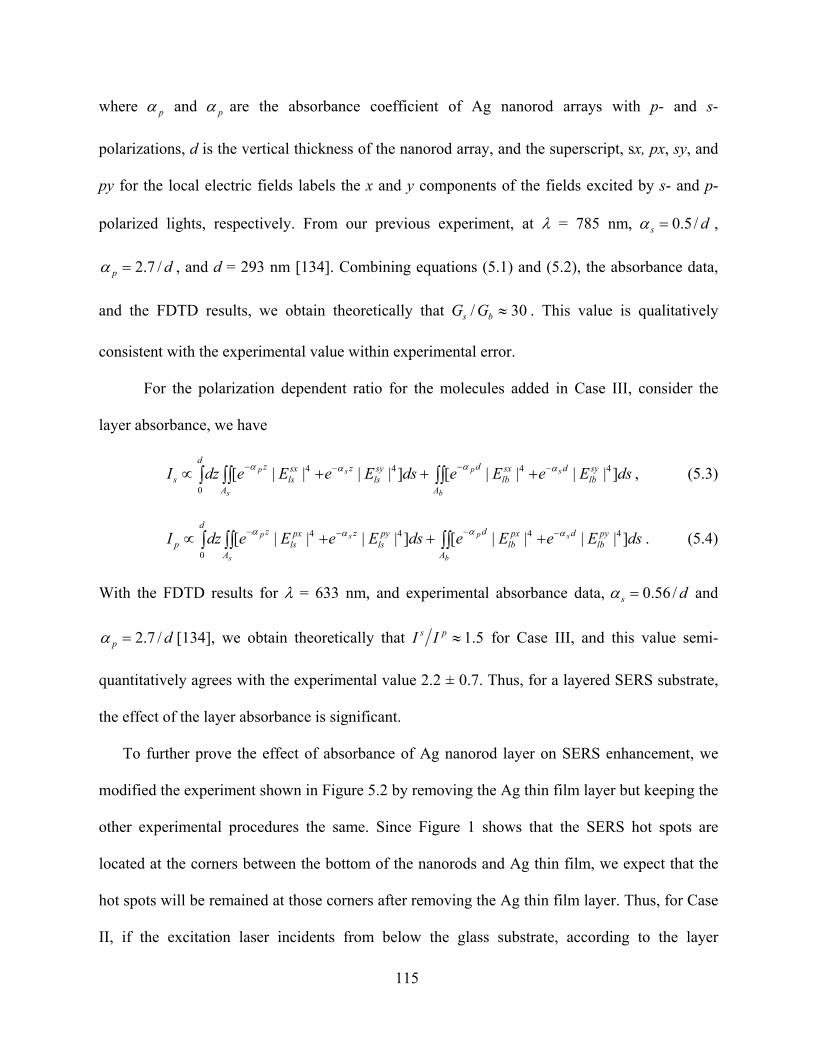
115
where pα and pα are the absorbance coefficient of Ag nanorod arrays with p- and s-
polarizations, d is the vertical thickness of the nanorod array, and the superscript, sx, px, sy, and
py for the local electric fields labels the x and y components of the fields excited by s- and p-
polarized lights, respectively. From our previous experiment, at λ = 785 nm, ds /5.0=α ,
dp /7.2=α , and d = 293 nm [134]. Combining equations (5.1) and (5.2), the absorbance data,
and the FDTD results, we obtain theoretically that 30/ ≈bs GG . This value is qualitatively
consistent with the experimental value within experimental error.
For the polarization dependent ratio for the molecules added in Case III, consider the
layer absorbance, we have
∫∫∫∫∫ −−−− +++∝b
sp
s
sp
A
sylb
dsxlb
d
A
syls
zsxls
zd
s dsEeEedsEeEedzI ]||||[]||||[ 4444
0
αααα , (5.3)
∫∫∫∫∫ −−−− +++∝b
sp
s
sp
A
pylb
dpxlb
d
A
pyls
zpxls
zd
p dsEeEedsEeEedzI ]||||[]||||[ 4444
0
αααα . (5.4)
With the FDTD results for λ = 633 nm, and experimental absorbance data, ds /56.0=α and
dp /7.2=α [134], we obtain theoretically that 5.1≈ps II for Case III, and this value semi-
quantitatively agrees with the experimental value 2.2 ± 0.7. Thus, for a layered SERS substrate,
the effect of the layer absorbance is significant.
To further prove the effect of absorbance of Ag nanorod layer on SERS enhancement, we
modified the experiment shown in Figure 5.2 by removing the Ag thin film layer but keeping the
other experimental procedures the same. Since Figure 1 shows that the SERS hot spots are
located at the corners between the bottom of the nanorods and Ag thin film, we expect that the
hot spots will be remained at those corners after removing the Ag thin film layer. Thus, for Case
II, if the excitation laser incidents from below the glass substrate, according to the layer
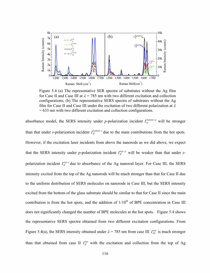
116
absorbance model, the SERS intensity under p-polarization incident pbottomIII − will be stronger
than that under s-polarization incident sbottomIII − due to the main contributions from the hot spots.
However, if the excitation laser incidents from above the nanorods as we did above, we expect
that the SERS intensity under p-polarization incident ptopIII − will be weaker than that under s-
polarization incident stopIII − due to absorbance of the Ag nanorod layer. For Case III, the SERS
intensity excited from the top of the Ag nanorods will be much stronger than that for Case II due
to the uniform distribution of SERS molecules on nanorods in Case III, but the SERS intensity
excited from the bottom of the glass substrate should be similar to that for Case II since the main
contribution is from the hot spots, and the addition of 1/10th of BPE concentration in Case III
does not significantly changed the number of BPE molecules at the hot spots. Figure 5.4 shows
the representative SERS spectra obtained from two different excitation configurations. From
Figure 5.4(a), the SERS intensity obtained under λ = 785 nm from case III topIIII is much stronger
than that obtained from case II topIII with the excitation and collection from the top of Ag
(b) (a)
1200 1300 1400 1500 1600 17000
10k
20k
30k
40k
50k
Ram
an In
tens
ity (c
ount
s)
I top-p II
I top-s II
I Bottom-s II
Raman Shift(cm-1)
I bottom-p II
1200 1300 1400 1500 1600 17000
1k2k3k4k5k6k7k8k
Ram
an In
tens
ity (c
ount
s)
Raman Shift (cm-1)
I topII
I bottomII
I topIII
I bottomIII
Figure 5.4 (a) The representative SER spectra of substrates without the Ag film for Case II and Case III at λ = 785 nm with two different excitation and collection configurations; (b) The representative SERS spectra of substrates without the Ag film for Case II and Case III under the excitation of two different polarization at λ = 633 nm with two different excitation and collection configurations.
117
nanorod, while the SERS intensity obtained from case III bottomIIII is almost the same as that
obtained from case II bottomIII with the excitation and collection from the bottom of glass substrate,
which is consistent with our prediction. For case II, under different polarization states and
incident configurations, Figure 5.4(b) shows that the SERS intensity obtained from the bottom is
obviously much stronger than that from the top. Under the excitation configuration from the
bottom, the SERS peak intensity at band 1200 cm-1 excited by p-polarization is larger than that
excited by s-polarization, and the polarization SERS peak intensity ratio
77.0/ ≈−− pbottomII
sbottomII II , while under the excitation configuration from the top, the SERS peak
intensity at band 1200 cm-1 excited by s-polarization is larger than that excited by p-polarization,
and the polarization SERS peak intensity ratio 8.1/ ≈−− ptopII
stopII II . These experimental results
strongly support the above experimental results and theoretical explanations. The anisotropic
absorbance by Ag nanorod layer for s- and p- polarizations Raman scattering plays an important
role in the SERS enhancement from Ag nanorod array substrates.
5.6 Conclusions
In summary, our experimental results have shown that although the bottom of Ag nanorod
with high local electric field sites can give a reasonable SERS signal, the dominant SERS
intensity comes from the surfaces of the Ag nanorods. The SERS intensity excited by s-
polarization is stronger than that excited by p-polarization under the excitation from the top of
Ag nanorod array with Ag film underlayer, while the SERS polarization dependence is reversed
under the excitation from the bottom of Ag nanorod array without Ag film underlayer. We
estimated the SERS enhancement factor from the nanorod surfaces is about 50 - 200 times that
at the bottom (surface on the Ag thin film). These results cannot be interpreted solely using the

118
local field enhancement. Rather, since the SERS substrate has a layer structure, the absorbance
of the scattered SERS signal can play a significant role. By considering the anisotropic
absorbance of the Ag layer, and combining with the FDTD calculations, we can theoretically
predict that the SERS enhancement factor at the nanorod surfaces is 30 times that at the bottom.
This model can also correctly give a correct explanation to the polarized SERS ratio. Our results
demonstrate that the “hot spots” are not necessarily the dominate SERS mechanism for all
nanostructures and all measurement configurations. For the structures with the “hot spots”
directly exposed to the SERS detector, the “hot spots” determine the SERS response. However,
for the “hot spots” not directly exposed to the detector, the effect of the “hot spots” on the SERS
intensity depends on the specific nanostructure, its optical properties and detection
configurations.

119
CHAPTER 6
CONCLUSIONS AND FUTURE WORK
In this dissertation, a new SERS substrate platform --- the Ag nanorod array substrate has
been systematically studied. It is found that Ag nanorod array substrates fabricated by oblique
angle deposition have a strong SERS activity, and the SERS enhancement factor can reach to 109.
Due to the special structure of Ag nanorod arrays, it shows some unique SERS characteristics. In
order to understand these SERS properties, modified Greenler’s model and layer absorbance
model are proposed to give some theoretical explanations. Except these characteristics, the origin
of SERS from Ag nanorod array has also been investigated.
Oblique angle deposition technique is a very simple technique to fabricate large area,
aligned tilting Ag nanorod arrays. The length, tilting angle, diameter and density of Ag nanorods
can be controlled by the deposition angle, deposition time and other deposition parameters. Both
the diameter and density of Ag nanorods follow power laws with the length of Ag nanorods, with
the exponents 34.0~30.0=p and 23.0~40.0 −−=γ for various deposition angles. For Ag
nanorods with the similar length, the larger deposition angle, the smaller diameter. However, all
these parameters cannot be controlled at designed values using normal OAD technique.
Fortunately, more ordered and uniform arranged Ag nanorod arrays can be fabricated by
template OAD technique combing EBL and OAD techniques, whose diameter, separation and
density of Ag nanorods can be adjusted by the parameters of seeds templates.

120
Due to the special structure of Ag nanorod arrays, the SERS intensity has been found strongly
dependent on the parameters relative to the excitation configurations such as incident angle,
polarization states and the underlayer: (1) The SERS intensity is closely related to the incident
angle. There is an optimal incident angle where the SERS intensity reaches its maximum. For
example, for the Ag nanorod array with ~900 nm length deposited at 86°, the optimum incident
angle is ~ 45°. (2) The underlayer thin film reflection has a significant effect on the SERS
intensity. The higher the reflectance is, the larger the SERS intensity is obtained. (3) The SERS
intensity is polarization dependent. For perpendicular Raman excitation, s-polarization excitation
contribute more SERS intensity than p-polarization. All these properties can be qualitatively
explained by a modified Greenler’s model.
The SERS intensity not only depends on the parameters relative to excitation
configurations, but also on the structural parameters of nanoparticles systems such as the length,
separation, diameter and shapes. For Ag nanorod arrays, the SERS intensity is strongly
dependent on the length of Ag nanorods and deposition angle, there is an optimum length for
SERS activity. The optimum diameter of Ag nanoparticles and nanorods is ~100 nm. Since the
separation of nanorods is not easy to control, the nanopost array fabricated by EBL to study the
separation dependence of SERS. It is found that the SERS intensity rapidly increases with the
decrease of the separation of nanoposts. To mimic the difference between Ag nanorod on glass
and Ag nanorods on Ag thin film, Au nanorod array and nanocomb array were fabricated by
EBL. Comparing these two different shapes, the nanospine of nanocomb plays an important role
in SERS activity.
In general, the largest SERS enhancement factor has been considered to generate from the
“hot spots” of nanoparticle systems. However, due to the special structure of Ag nanorod array,

121
the “hot spots” is buried in the bottom of Ag nanorods. We experimentally and theoretically
demonstrated that due to the anisotropic absorbance of Ag nanorod layer, most of SERS signal
come from the molecules adsorbed on the side surface of Ag nanorods, not from the so called
“hot spots” at the corner of between Ag nanorods and Ag film.
Although we performed a systematic studies on the SERS from Ag nanorod arrays
fabricated by OAD techniques, there are still several important aspects about SERS substrates
fabricated by OAD technique deserved to further investigations in the future. In SERS substrates
fabrication, we can employ OAD and substrates rotation so called “GLAD” technique to
fabricate vertical nanorod array, ZigZag array, spiral array and other shaped nanostructures, and
perform a systematic study on morphological, optical and SERS characterizations, and further
understand fundamental SERS mechanism for these substrates. We can also investigate other
material such as Cu, Ni and so on nanostructures fabricated by GLAD and study their SERS
characterizations and mechanism. Comparing the SERS responses from these nanostructres
fabricated by OAD or GLAD technique using different materials, one can find an optimum
SERS substrate. In this dissertation, the quality of semi-ordered Ag nanorod arrays fabricated by
template OAD technique is not very satisfied. It needs more and further works on template OAD
to fabricate more ordered and uniform Ag nanorod arrays, so that it can standardize the
uniformity and reproducibility for template Ag nanorod array SERS substrates. In addition, the
SERS mechanism of SERS from Ag nanorod arrays is also needed to pay more efforts, since
there is no direct model to explain the LSPR of Ag nanorod arrays. In addition, we also can work
on SERS related device based on Ag nanorod arrays such as SERS biochips and flowing cell and
so on.

122
REFERENCES
1. Shanmukh, S., Jones, L., Driskell, J., Zhao, Y., Dluhy, R., and Tripp, R. A., Rapid and
Sensitive Detection of Respiratory Virus Molecular Signatures Using a Silver Nanorod
Array SERS Substrate. Nano Lett., 2006. 6(11): p. 2630-2636.
2. Driskell, J. D., Primera-pedrozo, O. M., Dluhy, R. A., Zhao, Y. P., and Tripp, R. A.,
Quantitative Surface-Enhanced Raman Spectroscopy Based Analysis of MicroRNA
Mixtures. Appl. Spectrosc., 2009. 63(10): p. 1107-1114.
3. Tripp, R.A., R.A. Dluhy, and Y.-P. Zhao, Novel nanostructures for SERS biosensing.
Nano Today, 2008. 3(3-4): p. 31-37.
4. Hering. Katharina, Cialla.Dana., Ackermann. Katrin, Dörfer. Thomas, Möller. Robert,
Schneidewind. Henrik, Mattheis. Roland, Fritzsche. Wolfgang, Rösch. Petra, and Popp.
Jürgen, SERS: a versatile tool in chemical and biochemical diagnostics. Analytical &
Bioanalytical Chemistry, 2008. 390(1): p. 113-124.
5. Driskell, J.D., Shanmukh, S., Liu, Y. -J., Hennigan, S., Jones, L., Zhao, Y. P., Dluhy, R.
A., Krause, D. C., and Tripp, R. A., Infectious Agent Detection With SERS-Active Silver
Nanorod Arrays Prepared by Oblique Angle Deposition. Sensors Journal, IEEE, 2008.
8(6): p. 863-870.
6. Jarvis, R.M., A. Brooker, and R. Goodacre, Surface-enhanced Raman scattering for the
rapid discrimination of bacteria. Faraday Discussions, 2006. 132: p. 281-292.

123
7. Zhang, X., Young, M. A., Lyandres, O., and Van Duyne, R. P., Rapid Detection of an
Anthrax Biomarker by Surface-Enhanced Raman Spectroscopy. J. Am. Chem. Soc., 2005.
127(12): p. 4484-4489.
8. Ling, J., Weitman, S. D., Miller, M. A., Moore, R. V., and Bovik, A. C., Direct Raman
Imaging Techniques for Study of the Subcellular Distribution of a Drug. Appl. Opt., 2002.
41(28): p. 6006-6017.
9. Kneipp, K., Haka, A. S., Kneipp, H., Badizadegan, K., Yoshizawa, N., Boone, C., Shafer-
Peltier, K. E., Motz, J. T., Dasari, R. R. and Feld, M. S., Surface-Enhanced Raman
Spectroscopy in Single Living Cells Using Gold Nanoparticles. Applied Spectroscopy,
2002. 56: p. 150-154.
10. Qian, X.M. and S.M. Nie, Single-molecule and single-nanoparticle SERS: from
fundamental mechanisms to biomedical applications. Chemical Society Reviews, 2008.
37(5): p. 912-920.
11. Keren, S., Zavaleta, C., Cheng, Z., De la Zerda, A., Gheysens, O., and Gambhir, S. S.,
Noninvasive molecular imaging of small living subjects using Raman spectroscopy.
Proceedings of the National Academy of Sciences of the United States of America, 2008.
105(15): p. 5844-5849.
12. Zavaleta, C., De la Zerda, A., Liu, Z., Karen, S., Cheng, Z., Schipper, M., Chen, X., Dai,
H., and Gambhir, S. S, Noninvasive Raman Spectroscopy in Living Mice for Evaluation
of Tumor Targeting with Carbon Nanotubes. Nano Letters, 2008. 8(9): p. 2800-2805.
13. Singh, R., C. V. Raman and the Discovery of the Raman Effect. Physics in Perspective
(PIP), 2002. 4(4): p. 399-420.

124
14. Jarvis, R.M. and R. Goodacre, Characterisation and identification of bacteria using
SERS. Chemical Society Reviews, 2008. 37(5): p. 931-936.
15. Fleischmann, M., P.J. Hendra, and A.J. McQuillan, Raman spectra of pyridine adsorbed
at a silver electrode. Chemical Physics Letters, 1974. 26(2): p. 163-166.
16. Jeanmaire, D.L. and R.P. Van Duyne, Surface raman spectroelectrochemistry: Part I.
Heterocyclic, aromatic, and aliphatic amines adsorbed on the anodized silver electrode.
Journal of Electroanalytical Chemistry, 1977. 84(1): p. 1-20.
17. Gersten, J.I., R.L. Birke, and J.R. Lombardi, Theory of Enhance I Light Scattering from
Molecules Adsorbed at the Metal-Solution Interface. Physical Review Letters, 1979.
43(2): p. 147.
18. Aravind, P.K., A. Nitzan, and H. Metiu, The interaction between electromagnetic
resonances and its role in spectroscopic studies of molecules adsorbed on colloidal
particles or metal spheres. Surface Science, 1981. 110(1): p. 189-204.
19. Kerker, M., D.S. Wang, and H. Chew, Surface enhanced Raman scattering (SERS) by
molecules adsorbed at spherical particles. Appl. Opt., 1980. 19(19): p. 3373-3388.
20. Moskovits, M., Surface-enhanced spectroscopy. Reviews of Modern Physics, 1985. 57(3):
p. 783.
21. Zeman, E.J. and G.C. Schatz, An accurate electromagnetic theory study of surface
enhancement factors for silver, gold, copper, lithium, sodium, aluminum, gallium, indium,
zinc, and cadmium. The Journal of Physical Chemistry, 1987. 91(3): p. 634-643.
22. Wang, D.S., H. Chew, and M. Kerker, Enhanced Raman scattering at the surface (SERS)
of a spherical particle. Appl. Opt., 1980. 19(14): p. 2256-2257.

125
23. Dieringer, J.A., McFarland, A. D., Shah, N. C., Stuart, D. A., Whitney, A. V., Yonzon, C.
R., Young, M. A., Zhang, X. and Van Duyne, R. P., Introductory LectureSurface
enhanced Raman spectroscopy: new materials, concepts, characterization tools, and
applications. Faraday Discussions, 2006. 132: p. 9-26.
24. Yoon, I., Kang, T., Choi, W., Kim, J., Yoo, Y., Joo, S., Park, Q. H., Ihee, H., and Kim, B.,
Single Nanowire on a Film as an Efficient SERS-Active Platform. Journal of the
American Chemical Society, 2009. 131(2): p. 758-762.
25. Ray, G., Eugenia, K., Ikjun, C., and Vladimir, V. T., Bimetallic Nanostructures as Active
Raman Markers: Gold-Nanoparticle Assembly on 1D and 2D Silver Nanostructure
Surfaces. Small, 2009. 5(21): p. 2460.
26. Nicholas, C.L., Sun, C., Arya, A., Jiang, P., and Jiang, B., Surface-enhanced Raman
scattering on periodic metal nanotips with tunable sharpness. Nanotechnology, 2009(22):
p. 225303.
27. Musumeci, A., Gosztola, D., Schiller, T., Dimitrijevic, N. M., Mujica, V., Martine, D.,
and Rajh, T.., SERS of Semiconducting Nanoparticles (TiO2 Hybrid Composites). Journal
of the American Chemical Society, 2009. 131(17): p. 6040-6041.
28. Chen, L.-Y., Yu, J. -S., Fujita, T., and Chen, M. -W., Nanoporous Copper with Tunable
Nanoporosity for SERS Applications. Advanced Functional Materials, 2009. 19(8): p.
1221.
29. Liao, Q., Cheng, M., Xu, D. -S., Ai, X. -C., Yao, J. -N., and Zhang, J. -P., Gold Nanorod
Arrays with Good Reproducibility for High-Performance Surface-Enhanced Raman
Scattering. Langmuir, 2009. 25(8): p. 4708-4714.

126
30. Li, K., Clime, L., Cui, B., and Veres, T., Surface enhanced Raman scattering on long-
range ordered noble-metal nanocrescent arrays. Nanotechnology, 2008(14): p. 145305.
31. Lal, S., Grady, N. K., Kundu, J., Levin, C. S., Lassiter, J. B., and Halas, N. J., Tailoring
plasmonic substrates for surface enhanced spectroscopies. Chemical Society Reviews,
2008. 37(5): p. 898-911.
32. Kondo, T., Matsumoto, F., Nishio, K., and Masuda, H., Surface-enhanced Raman
Scattering on Ordered Gold Nanodot Arrays Prepared from Anodic Porous Alumina
Mask. Chemistry Letters, 2008. 37(4): p. 466-467.
33. Hyunhyub, K. and V.T. Vladimir, Nanoparticle-Decorated Nanocanals for Surface-
Enhanced Raman Scattering. Small, 2008. 4(11): p. 1980-1984.
34. Alvarez-Puebla, R., Cui, B., Bravo-Vasquez, J. P., Veres, T., and Fenniri, H.,
Nanoimprinted SERS-Active Substrates with Tunable Surface Plasmon Resonances. J.
Phys. Chem. C, 2007. 111(18): p. 6720-6723.
35. Schierhorn, M. Lee, S. J., Boettcher, S. W., Stucky, G. D., and Moskovits, M., Metal-
Silica Hybrid Nanostructures for Surface-Enhanced Raman Spectroscopy. Advanced
Materials, 2006. 18(21): p. 2829-2832.
36. Zhang, J., Li, X., Sun, X., and Li, Y., Surface Enhanced Raman Scattering Effects of
Silver Colloids with Different Shapes. J. Phys. Chem. B, 2005. 109(25): p. 12544-12548.
37. Chaney, S.B., Shanmukh, S., Dluhy, R. A., and Zhao, Y. P., Aligned silver nanorod
arrays produce high sensitivity surface-enhanced Raman spectroscopy substrates.
Applied Physics Letters, 2005. 87(3): p. 031908.
38. Nikoobakht, B. and M.A. El-Sayed, Surface-Enhanced Raman Scattering Studies on
Aggregated Gold Nanorods. J. Phys. Chem. A, 2003. 107(18): p. 3372-3378.

127
39. Felidj, N., Aubard, J., Levi, G., Krenn, J. R., Hohenau, A., Schider, G., Leitner, A., and
Aussenegg, F. R., Optimized surface-enhanced Raman scattering on gold nanoparticle
arrays. Applied Physics Letters, 2003. 82(18): p. 3095.
40. Alexander, W., Beomseck, K., Bryce, S., and Steven, L. T., Tunable Surface-Enhanced
Raman Scattering from Large Gold Nanoparticle Arrays. ChemPhysChem, 2001. 2(12):
p. 743-745.
41. Michaels, A.M., M. Nirmal, and L.E. Brus, Surface Enhanced Raman Spectroscopy of
Individual Rhodamine 6G Molecules on Large Ag Nanocrystals. J. Am. Chem. Soc.,
1999. 121(43): p. 9932-9939.
42. Nie, S. and S.R. Emory, Probing Single Molecules and Single Nanoparticles by Surface-
Enhanced Raman Scattering. Science, 1997. 275(5303): p. 1102-1106.
43. Kneipp, K., Wang, Y., Kneipp, H., perelman, L. T., Itzkan, I., Dasari, R. R., and Feld, M.
S., Single Molecule Detection Using Surface-Enhanced Raman Scattering (SERS).
Physical Review Letters, 1997. 78(9): p. 1667.
44. Brinkmann, U., SERS traces water pollution in real time. Laser Focus World, 2004. 40(6):
p. 15-19.
45. Viets, C. and W. Hill, Comparison of fibre-optic SERS sensors with differently prepared
tips. Sensors and Actuators B: Chemical, 1998. 51(1-3): p. 92-99.
46. Mullen, K.I. and K.T. Carron, Surface-enhanced Raman spectroscopy with abrasively
modified fiber optic probes. Anal. Chem., 1991. 63(19): p. 2196-2199.
47. Bello, J. M., Narayanan, V. A., Stokes, D. L., and Vo Dinh, T., Fiber-optic remote sensor
for in situ surface-enhanced Raman scattering analysis. Anal. Chem., 1990. 62(22): p.
2437-2441.
128
48. Premasiri, W. R., moir, D. T., Klempner, M. S., Krieger, N., Jones, G., and Ziegler, L. D.,
Characterization of the Surface Enhanced Raman Scattering (SERS) of Bacteria. J. Phys.
Chem. B, 2005. 109(1): p. 312-320.
49. Jarvis, R.M. and R. Goodacre, Discrimination of Bacteria Using Surface-Enhanced
Raman Spectroscopy. Anal. Chem., 2004. 76(1): p. 40-47.
50. Stokes, D. L., Z. Chi, and T. Vo-Dinh, Surface-Enhanced-Raman-Scattering-Inducing
Nanoprobe for Spectrochemical Analysis. Applied Spectroscopy, 2004. 58(3): p. 292-298.
51. Vo-Dinh, T., Stokes, D. L., Griffin, G. D., Volkan, M., Kim, U. J., and Simon, M. J.,
Surface-enhanced Raman Scattering (SERS) method and instrumentation for genomics
and biomedical analysis. Journal of Raman Spectroscopy, 1999. 30(9): p. 785-793.
52. Choo-Smith, L. -P. Edwards, H. G. M., Endtz, H. P., Kros, J. M., Heule, F., Barr, H.,
Robinson Jrs, J. S., Bruining, H. A., and Puppels, G. J., Medical applications of Raman
spectroscopy: From proof of principle to clinical implementation. Biopolymers, 2002.
67(1): p. 1-9.
53. Shim, M.G. and B.C. Wilson, Development of an In Vivo Raman Spectroscopic System
for Diagnostic Applications. Journal of Raman Spectroscopy, 1997. 28(2-3): p. 131-142.
54. Ruan, C., W. Wang, and B. Gu, Surface-enhanced Raman scattering for perchlorate
detection using cystamine-modified gold nanoparticles. Analytica Chimica Acta, 2006.
567(1): p. 114-120.
55. Steinfeld, J.I. and J. Wormhoudt, EXPLOSIVES DETECTION: A Challenge for Physical
Chemistry. Annual Review of Physical Chemistry, 1998. 49(1): p. 203-232.
56. Vitaliy, N.P. and V.S. Tigran, Surface-enhanced Raman scattering on the nanoscale: a
microscopic approach. Journal of Optics A: Pure and Applied Optics, 2006(4): p. S208.

129
57. Otto, A., Mrozek, I., Grabhorn, H., and Akemann, W., Surface-enhanced Raman
scattering. Journal of Physics: Condensed Matter, 1992(5): p. 1143.
58. Moskovits, M., Surface-enhanced Raman spectroscopy: a brief retrospective. Journal of
Raman Spectroscopy, 2005. 36(6-7): p. 485-496.
59. Campion, A. and P. Kambhampati, Surface-enhanced Raman scattering. Chemical
Society Reviews 1998. 27(4): p. 10.
60. Saikin, S.K., Olivares-Amaya, R., Rappopport, D., Stopa, M., Aspuru-Guzik, A., On the
chemical bonding effects in the Raman response: Benzenethiol adsorbed on silver
clusters. Physical Chemistry Chemical Physics, 2009. 11(41): p. 9401-9411.
61. Wu, D.-Y., Liu, X. -M., Duan, S., Xu, X., Ren, B., Lin, S. -S., and Tian, Z. -Q., Chemical
Enhancement Effects in SERS Spectra: A Quantum Chemical Study of Pyridine
Interacting with Copper, Silver, Gold and Platinum Metals. The Journal of Physical
Chemistry C, 2008. 112(11): p. 4195-4204.
62. John, R.L., Ronald, L. B., Lu, T., and Xu, J., Charge-transfer theory of surface enhanced
Raman spectroscopy: Herzberg--Teller contributions. The Journal of Chemical Physics,
1986. 84(8): p. 4174-4180.
63. Frank, J.A., Charge transfer effects in surface-enhanced Raman scattering. The Journal
of Chemical Physics, 1982. 77(11): p. 5302-5314.
64. Arenas, J.F., Woolley, M. S., Otero, J. C., and Marcos, J. I., Charge-Transfer Processes
in Surface-Enhanced Raman Scattering. Franck-Condon Active Vibrations of Pyrazine.
The Journal of Physical Chemistry, 1996. 100(8): p. 3199-3206.

130
65. Yoon, J.H., J.S. Park, and S. Yoon, Time-Dependent and Symmetry-Selective Charge-
Transfer Contribution to SERS in Gold Nanoparticle Aggregates. Langmuir, 2009.
25(21): p. 12475-12480.
66. Campion, A., Ivanecky, J. E., Child, C. M., and Foster, M., On the Mechanism of
Chemical Enhancement in Surface-Enhanced Raman Scattering. Journal of the American
Chemical Society, 1995. 117(47): p. 11807-11808.
67. David, P.F., Arvind, S., Anika, K., Schuck, P. J., Gordon, S. K., and Moerner, W. E.,
Exploring the chemical enhancement for surface-enhanced Raman scattering with Au
bowtie nanoantennas. The Journal of Chemical Physics, 2006. 124(6): p. 061101.
68. Polubotko, A.M., Manifestation of electrodynamical forbiddance of the quadrupole SERS
mechanism in the methane molecule. Optics Communications, 1996. 127(1-3): p. 135-
143.
69. Schatz, G., M. Young, and R. Van Duyne, Electromagnetic Mechanism of SERS, in
Surface-Enhanced Raman Scattering. 2006. p. 19-45.
70. Katrin, K., Harald, K., Irving, I., Ramachandra, R. D., and Michael, S. F., Surface-
enhanced Raman scattering and biophysics. Journal of Physics: Condensed Matter,
2002(18): p. R597.
71. Kelly, K.L., Coronado, E., Zhao, L. L., and Schatz, G. C., The Optical Properties of
Metal Nanoparticles: The Influence of Size, Shape, and Dielectric Environment. J. Phys.
Chem. B, 2003. 107(3): p. 668-677.
72. Xu, H., Aizpurua, J., Käll, M., and Apell, P., Electromagnetic contributions to single-
molecule sensitivity in surface-enhanced Raman scattering. Physical Review E, 2000.
62(3): p. 4318.

131
73. Camden, J.P., Dieringer, J. A., Wang, Y., Masiello, D. J., Marks, L. D., Schatz, G. C.,
and Van Duyne, R. P., Probing the Structure of Single-Molecule Surface-Enhanced
Raman Scattering Hot Spots. Journal of the American Chemical Society, 2008. 130(38):
p. 12616-12617.
74. Hao, E. and G.C. Schatz, Electromagnetic fields around silver nanoparticles and dimers.
The Journal of Chemical Physics, 2004. 120(1): p. 357-366.
75. Aizpurua, J., Hanarp, P., Sutherland, D. S., Käll, M., Bryant, G. W., and García de Abajo,
F. J., Optical Properties of Gold Nanorings. Physical Review Letters, 2003. 90(5): p.
057401.
76. Lu, Y., Liu, G. L., Kim, J., Mejia, Y. X., and Lee, L. P., Nanophotonic Crescent Moon
Structures with Sharp Edge for Ultrasensitive Biomolecular Detection by Local
Electromagnetic Field Enhancement Effect. Nano Lett., 2005. 5(1): p. 119-124.
77. Talley, C.E., Jackson, J. B., Oubre, C., Grady, N. K., Hollars, C. W., Lane, S. M., Huser,
T. R., Nordlander, P., and Halas, N. J., Surface-Enhanced Raman Scattering from
Individual Au Nanoparticles and Nanoparticle Dimer Substrates. Nano Letters, 2005.
5(8): p. 1569-1574.
78. Le Ru, E.C. and P.G. Etchegoin, Sub-wavelength localization of hot-spots in SERS.
Chemical Physics Letters, 2004. 396(4-6): p. 393-397.
79. Qin, L., Zou, S., Xue, C., Atkinson, A., Schatz, G. C., and Mirkin, C. A., Designing,
fabricating, and imaging Raman hot spots. Proceedings of the National Academy of
Sciences, 2006. 103(36): p. 13300-13303.

132
80. Guillaume, L., Nordin, F., Johan, G., Jean, A., Georges, L., Andreas, H., Franz, R. A.,
and Joachim, R. K., Raman scattering images and spectra of gold ring arrays. Physical
Review B (Condensed Matter and Materials Physics), 2006. 73(24): p. 245417.
81. Banholzer, M.J., Millstone, J. E., Qin, L., and Mirkin, C. A., Rationally designed
nanostructures for surface-enhanced Raman spectroscopy. Chemical Society Reviews,
2008. 37(5): p. 885-897.
82. Ward, D.R., Grady, N. K., Levin, C. S., Halas, N. J., Wu, Y., Nordlander, P., and
Natelson, D., Electromigrated Nanoscale Gaps for Surface-Enhanced Raman
Spectroscopy. Nano Letters, 2007. 7(5): p. 1396-1400.
83. Willets, K.A. and R.P. Van Duyne, Localized Surface Plasmon Resonance Spectroscopy
and Sensing. Annual Review of Physical Chemistry, 2007. 58(1): p. 267-297.
84. Moreno, E., Erni, D., Hafner, C., and Vahldieck, R., Multiple multipole method with
automatic multipole setting applied to the simulation of surface plasmons in metallic
nanostructures. J. Opt. Soc. Am. A, 2002. 19(1): p. 101-111.
85. Novotny, L., D.W. Pohl, and B. Hecht, Scanning near-field optical probe with ultrasmall
spot size. Opt. Lett., 1995. 20(9): p. 970-972.
86. Chiappetta, P., Multiple scattering approach to light scattering by arbitrarily shaped
particles. Journal of Physics A: Mathematical and General, 1980(6): p. 2101.
87. Zhang, Z.Y. and Y.P. Zhao, Optical properties of helical Ag nanostructures calculated by
discrete dipole approximation method. Applied Physics Letters, 2007. 90(22): p. 221501.
88. Laczik, Z., Discrete-dipole-approximation-based light-scattering calculations for
particles with a real refractive index smaller than unity. Appl. Opt., 1996. 35(19): p.
3736-3745.

133
89. Draine, B.T. and P.J. Flatau, Discrete-dipole approximation for scattering calculations. J.
Opt. Soc. Am. A, 1994. 11(4): p. 1491-1499.
90. Liu, Y.J., Zhang, Z. Y., Zhao, Q., Dluhy, R. A., and Zhao, Y. P., The role of the
nanospine in the nanocomb arrays for surface enhanced Raman scattering. Applied
Physics Letters, 2009. 94(3): p. 033103.
91. Liu, Y.-J., Zhang, Z.-Y., Zhao, Q., and Zhao, Y.-P., Revisiting the separation dependent
surface enhanced Raman scattering. Applied Physics Letters, 2008. 93(17): p. 173106.
92. Oubre, C. and P. Nordlander, Finite-difference Time-domain Studies of the Optical
Properties of Nanoshell Dimers. J. Phys. Chem. B, 2005. 109(20): p. 10042-10051.
93. Mur, G., Absorbing Boundary Conditions for the Finite-Difference Approximation of the
Time-Domain Electromagnetic-Field Equations. IEEE Transactions on Electromagnetic
Compatibility, 1981. EMC-23(4): p. 6.
94. Taflove, A. and M.E. Brodwin, Numerical Solution of Steady-State Electromagnetic
Scattering Problems Using the Time-Dependent Maxwell's Equatio. IEEE Transactions
on Microwave Theory and Techniques, 1975. 23(8): p. 8.
95. Yee, K., Numerical solution of initial boundary value problems involving maxwell's
equations in isotropic media. IEEE Transactions on Antennas and Propagation, 1966.
14(3): p. 6.
96. Link, S. and M.A. El-Sayed, Spectral Properties and Relaxation Dynamics of Surface
Plasmon Electronic Oscillations in Gold and Silver Nanodots and Nanorods. The Journal
of Physical Chemistry B, 1999. 103(40): p. 8410-8426.

134
97. Gunnarsson, L., Rindzevicius, T., Prikulis, J., Kasemo, B., Kall, M., Zou, S., Confined
Plasmons in Nanofabricated Single Silver Particle Pairs: Experimental Observations of
Strong Interparticle Interactions. J. Phys. Chem. B, 2005. 109(3): p. 1079-1087.
98. Chan, G.H., Zhao, J., Schatz, G. C., and Van Duyne, R. P., Localized Surface Plasmon
Resonance Spectroscopy of Triangular Aluminum Nanoparticles. The Journal of Physical
Chemistry C, 2008. 112(36): p. 13958-13963.
99. Aizpurua, J., Garnett, W. B., Lee, J. R., Abajo, Garcia de Abajo, F. J., Brian, K. K., and
Mallouk, T., Optical properties of coupled metallic nanorods for field-enhanced
spectroscopy. Physical Review B (Condensed Matter and Materials Physics), 2005.
71(23): p. 235420.
100. Mock, J.J., Barbic, M., Smith, D. R., Schultz, D. A., and Schultz, S., Shape effects in
plasmon resonance of individual colloidal silver nanoparticles. The Journal of Chemical
Physics, 2002. 116(15): p. 6755-6759.
101. Su, K.H., Wei, Q. H., Zhang, X., Mock, J. J., Smith, D. R., and Schultz, S., Interparticle
Coupling Effects on Plasmon Resonances of Nanogold Particles. Nano Lett., 2003. 3(8):
p. 1087-1090.
102. Ke, Z., Troparevsky, M. C., Di, X., Adolfo, G. E., and Zhenyu, Z., Electronic Coupling
and Optimal Gap Size between Two Metal Nanoparticles. Physical Review Letters, 2009.
102(18): p. 186804.
103. Zou, S. and G.C. Schatz, Narrow plasmonic/photonic extinction and scattering line
shapes for one and two dimensional silver nanoparticle arrays. The Journal of Chemical
Physics, 2004. 121(24): p. 12606-12612.

135
104. Zou, S., N. Janel, and G.C. Schatz, Silver nanoparticle array structures that produce
remarkably narrow plasmon lineshapes. The Journal of Chemical Physics, 2004. 120(23):
p. 10871-10875.
105. Zhao, L., K.L. Kelly, and G.C. Schatz, The Extinction Spectra of Silver Nanoparticle
Arrays: Influence of Array Structure on Plasmon Resonance Wavelength and Width. The
Journal of Physical Chemistry B, 2003. 107(30): p. 7343-7350.
106. Zou, S. and G.C. Schatz, Silver nanoparticle array structures that produce giant
enhancements in electromagnetic fields. Chemical Physics Letters, 2005. 403(1-3): p. 62-
67.
107. Hicks, E.M., Zou, S., Schatz, G. C., Spears, K. G., Van Duyne, R. P., Gunnarsson, L.,
Rindzevicius, T., Kasemo, B., and Kall, M., Controlling Plasmon Line Shapes through
Diffractive Coupling in Linear Arrays of Cylindrical Nanoparticles Fabricated by
Electron Beam Lithography. Nano Letters, 2005. 5(6): p. 1065-1070.
108. Grand, J., Lamy de la Chapelle, M., Bijeon, J. L., Adam, P. M., Vial, A., and Royer, P.,
Role of localized surface plasmons in surface-enhanced Raman scattering of shape-
controlled metallic particles in regular arrays. Physical Review B (Condensed Matter
and Materials Physics), 2005. 72(3): p. 033407.
109. Tian, Z.-Q., B. Ren, and D.-Y. Wu, Surface-Enhanced Raman Scattering: From Noble to
Transition Metals and from Rough Surfaces to Ordered Nanostructures. The Journal of
Physical Chemistry B, 2002. 106(37): p. 9463-9483.
110. Ahern, A.M. and R.L. Garrell, In situ photoreduced silver nitrate as a substrate for
surface-enhanced Raman spectroscopy. Analytical Chemistry, 1987. 59(23): p. 2813-
2816.

136
111. Xue, G., J. Dong, and M. Zhang, Surface-Enhanced Raman Scattering (SERS) and
Surface-Enhanced Resonance Raman Scattering (SERRS) on HNO3-Roughened Copper
Foil. Applied Spectroscopy, 1991. 45: p. 756-759.
112. Neddersen, J., G. Chumanov, and T.M. Cotton, Laser Ablation of Metals: A New Method
for Preparing SERS Active Colloids. Applied Spectroscopy, 1993. 47: p. 1959-1964.
113. Schlegel, V.L. and T.M. Cotton, Silver-island films as substrates for enhanced Raman
scattering: effect of deposition rate on intensity. Analytical Chemistry, 1991. 63(3): p.
241-247.
114. Roark, S.E., D.J. Semin, and K.L. Rowlen, Quantitative Evaluation of SERS-Active Ag
Film Nanostructure by Atomic Force Microscopy. Analytical Chemistry, 1996. 68(3): p.
473-480.
115. Taylor, C.E., S.D. Garvey, and J.E. Pemberton, Carbon Contamination at Silver Surfaces:
Surface Preparation Procedures Evaluated by Raman Spectroscopy and X-ray
Photoelectron Spectroscopy. Analytical Chemistry, 1996. 68(14): p. 2401-2408.
116. Ratna, T., J.C.B. Richard, and J.T.M. Martin, Strategy to improve the reproducibility of
colloidal SERS. Journal of Raman Spectroscopy, 2007. 38(11): p. 1469-1479.
117. Murphy, C.J., Sau, T. K., Gole, A. M., Orendorff, C. J., Gao, J., Gou, L., Hunyadi, S. E.,
and Li, T., Anisotropic Metal Nanoparticles: Synthesis, Assembly, and Optical
Applications. J. Phys. Chem. B, 2005. 109(29): p. 13857-13870.
118. Lombardi, I., Cavallotti, P. L., Carraro, C., and Maboudian, R., Template assisted
deposition of Ag nanoparticle arrays for surface-enhanced Raman scattering
applications. Sensors and Actuators B: Chemical, 2007. 125(2): p. 353-356.

137
119. Ruan, C., Eres, G., Wang, W., Zhang, Z., and Gu, B., Controlled Fabrication of
Nanopillar Arrays as Active Substrates for Surface-Enhanced Raman Spectroscopy.
Langmuir, 2007. 23(10): p. 5757-5760.
120. Haynes, C.L. and R.P. Van Duyne, Nanosphere Lithography: A Versatile
Nanofabrication Tool for Studies of Size-Dependent Nanoparticle Optics. J. Phys. Chem.
B, 2001. 105(24): p. 5599-5611.
121. Zhang, X., C.R. Yonzon, and R.P. Van Duyne, Nanosphere lithography fabricated
plasmonic materials and their applications. J. Mater. Res., 2006. 21(5): p. 1083.
122. Jensen, T.R., Malinsky, M. D., Haynes, C. L., and Van Duyne, R. P., Nanosphere
Lithography: Tunable Localized Surface Plasmon Resonance Spectra of Silver
Nanoparticles. The Journal of Physical Chemistry B, 2000. 104(45): p. 10549-10556.
123. Haes, A.J., Haynes, C. L., McCabe, A. D., Schatz, G. C., Van Duyne, R. P., ans Zou, S.,
Plasmonic Materials for Surface-enhanced Sensing and Spectroscopy. MRS BULLETIN,
2005. 30: p. 368.
124. Grand, J., Kostcheev, S., Bijeon, J. L., de la Chapelle, M. L., Adam, P. M., Rumyantseva,
A., Lerondel, G., and Royer, P., Optimization of SERS-active substrates for near-field
Raman spectroscopy. Synthetic Metals, 2003. 139(3): p. 621-624.
125. Feidj, N., Aubard, J., Lei, G., Krenn, J. R., Salerno, M., Schider, G., Lamprecht, B.,
Leitner, A., and Aussenegg, F. R., Controlling the optical response of regular arrays of
gold particles for surface-enhanced Raman scattering. Physical Review B, 2002. 65(7): p.
075419.

138
126. Gunnarsson, L., Bjerneld, E. J., Xu, H., Petronis, S., Kasemo, B., and Kall, M et al.,
Interparticle coupling effects in nanofabricated substrates for surface-enhanced Raman
scattering. Applied Physics Letters, 2001. 78(6): p. 802-804.
127. Gopinath, A., Boriskina, S. V., Reinhard, B. M., and Dal Negro, L., Deterministic
aperiodic arrays of metal nanoparticles for surface-enhanced Raman scattering (SERS).
Opt. Express, 2009. 17(5): p. 3741-3753.
128. Yu, Q., Guan, P., Qin, D., Golden, G., and Wallace, P. M., Inverted Size-Dependence of
Surface-Enhanced Raman Scattering on Gold Nanohole and Nanodisk Arrays. Nano
Letters, 2008. 8(7): p. 1923-1928.
129. Felidj, N., Truong, S. L., Aubard, J., Levi, G., Krenn, J. R., Hohenau, A., Leitner, A., and
Aussenegg, F. R., Gold particle interaction in regular arrays probed by surface
enhanced Raman scattering. The Journal of Chemical Physics, 2004. 120(15): p. 7141-
7146.
130. Liu, Y.-J., Zhang, Z.-Y., Zhao, Q., Dluhy, R. A., and Zhao, Y.-P., The surface enhanced
Raman scattering from Ag nanorod array substrate: the site dependent enhancement and
layer absorbance effect. J. Phys. Chem. C, 2009.
131. Liu, Y.-J., Zhang, Z.-Y., Dluhy, R. A., and Zhao, Y.-P., SERS response of semi-ordered
Ag nanorod arrays. Journal of Raman Spectroscopy, 2009.
132. Driskell, J.D., Shanmukh, S., Liu, Y.-J., Chaney, S. B., Tang, X. J., Zhao, Y. P., and
Dluhy, R. A., The Use of Aligned Silver Nanorod Arrays Prepared by Oblique Angle
Deposition as Surface Enhanced Raman Scattering Substrates. J. Phys. Chem. C, 2008.
112(4): p. 895-901.

139
133. Zhao, Y.P., Chaney, S.B., and Zhang, Z.Y., Absorbance spectra of aligned Ag nanorod
arrays prepared by oblique angle deposition. Journal of Applied Physics, 2006. 100(6): p.
063527.
134. Zhao, Y.P., Chaney, S. B., Shanmukh, S., Dluhy, R. A., Polarized Surface Enhanced
Raman and Absorbance Spectra of Aligned Silver Nanorod Arrays. J. Phys. Chem. B,
2006. 110(7): p. 3153-3157.
135. Liu, Y.-J., Fan, J.-G., Zhao, Y.-P., Shanmukh, S., and Dluhy, R. A., Angle dependent
surface enhanced Raman scattering obtained from a Ag nanorod array substrate.
Applied Physics Letters, 2006. 89(17): p. 053117.
136. Billot, L., Lamy de la Chapelle, M., Grimault, A. S., Vial, A., Barchiesi, D., Bijeon, J. L.,
Adam, P. M., and Royer, P., Surface enhanced Raman scattering on gold nanowire
arrays: Evidence of strong multipolar surface plasmon resonance enhancement.
Chemical Physics Letters, 2006. 422(4-6): p. 303-307.
137. Xu, H. and Käll, M., Polarization-Dependent Surface-Enhanced Raman Spectroscopy of
Isolated Silver Nanoaggregates. ChemPhysChem, 2003. 4(9): p. 1001-1005.
138. Tao, A.R. and Yang, P., Polarized Surface-Enhanced Raman Spectroscopy on Coupled
Metallic Nanowires. J. Phys. Chem. B, 2005. 109(33): p. 15687-15690.
139. kundt, A., On the Double Refraction of Light in Metal Layers Which have been Prepared
by Kathode Sputtering. Ann. Phys. Chem., 1886. 27.
140. Holland, L., The Effect of Vapor Incidence on the Structure of Evaporated Aluminum
Films. J. Opt. Soc. Am., 1953. 43(5): p. 376-380.
141. Smith, D.O., Anisotropy in Permalloy Films. Journal of Applied Physics, 1959. 30(4): p.
S264-S265.

140
142. Young, N.O. and Kowal, J., Optically Active Fluorite Films. Nature, 1959. 183(4654): p.
104-105.
143. Nieuwenhuizen, J.M. and Haanstra, H.B., Microfractography of thin films. Philips Tech.
Rev., 1966. 27: p. 87-89.
144. Robbie, K. and Brett, M.J.. Sculptured thin films and glancing angle deposition: Growth
mechanics and applications. 1997: AVS.
145. Smith, D.O., Cohen, M.S., and Weiss, G.P., Oblique-Incidence Anisotropy in Evaporated
Permalloy Films. Journal of Applied Physics, 1960. 31(10): p. 1755-1762.
146. Robbie, K., Sit, J.C., and Brett, M.J., Advanced techniques for glancing angle deposition.
Journal of Vacuum Science & Technology B: Microelectronics and Nanometer Structures,
1998. 16(3): p. 1115-1122.
147. Kiema, G.K., Colgan, M.J., and Brett, M.J., Dye sensitized solar cells incorporating
obliquely deposited titanium oxide layers. Solar Energy Materials and Solar Cells, 2005.
85(3): p. 321-331.
148. Tansel, K., James, S. D., Pei, I. W., Gregory, A. T. E., Dexian, Y., Wang, G. -C., Lu, T. -
M., Low temperature melting of copper nanorod arrays. Journal of Applied Physics,
2006. 99(6): p. 064304.
149. Kar, A.K., Morrow, P., Tang, X. T., Parker, T. C., Li, H., Dai, J. Y., Shima, M., and
Wang, G. C., Epitaxial multilayered Co/Cu ferromagnetic nanocolumns grown by
oblique angle deposition. Nanotechnology, 2007(29): p. 295702.
150. He, Y. -P., Wu, J., and Zhao, Y. -P, Designing Catalytic Nanomotors by Dynamic
Shadowing Growth. Nano Letters, 2007. 7(5): p. 1369-1375.

141
151. Tait, R.N., Smy, T., and Brett, M.J., Modelling and characterization of columnar growth
in evaporated films. Thin Solid Films, 1993. 226(2): p. 196-201.
152. Ye, D.X., Karabacak, T., Lim, B. K., Wang, G. C., and Lu, T. M., Growth of uniformly
aligned nanorod arrays by oblique angle deposition with two-phase substrate rotation.
Nanotechnology, 2004(7): p. 817.
153. Matthew, M.H. and Michael, J.B., Glancing angle deposition: Fabrication, properties,
and applications of micro- and nanostructured thin films. Journal of Vacuum Science &
Technology A: Vacuum, Surfaces, and Films, 2007. 25(5): p. 1317-1335.
154. Smith, W., Ingram, W., and Zhao, Y., The scaling of the photocatalytic decay rate with
the length of aligned TiO2 nanorod arrays. Chemical Physics Letters, 2009. 479(4-6): p.
270-273.
155. Cristina, B., Gisia, B., Chelsea, E., and Kevin, R., Control of power law scaling in the
growth of silicon nanocolumn pseudo-regular arrays deposited by glancing angle
deposition. Nanotechnology, 2005(10): p. 1986.
156. Karabacak, T., Singh, J. P., Zhao, Y. P., Wang, G. C., and Lu, T. M., Scaling during
shadowing growth of isolated nanocolumns. Physical Review B, 2003. 68(12): p. 125408.
157. Yu, J. and Amar, J. G., Dynamical scaling behavior in two-dimensional ballistic
deposition with shadowing. Physical Review E, 2002. 66(2): p. 021603.
158. Robbie, K., Friedrich, L. J., Dew, S. K., Smy, T., and Brett, M. J., Fabrication of thin
films with highly porous microstructures. Journal of Vacuum Science & Technology A:
Vacuum, Surfaces, and Films, 1995. 13(3): p. 1032-1035.
159. Zhao, Y.P., Ye, D. X., Wang, G. C., and Lu, T. M., Novel Nano-Column and Nano-
Flower Arrays by Glancing Angle Deposition. Nano Letters, 2002. 2(4): p. 351-354.

142
160. Ye, D.X., Karabacak, T., Picu, R. C., Wang, G. C., and Lu, T. M., Uniform Si
nanostructures grown by oblique angle deposition with substrate swing rotation.
Nanotechnology, 2005. 16(9): p. 1717.
161. Jensen, M.O., and Brett, M.J., Periodically structured glancing angle deposition thin
films. Nanotechnology, IEEE Transactions on, 2005. 4(2): p. 269-277.
162. Hrudey, P. C. P., Westra, K. L., and Brett, M. J., Highly Ordered Organic Alq3 Chiral
Luminescent Thin Films Fabricated by Glancing-Angle Deposition. Advanced Materials,
2006. 18(2): p. 224-228.
163. Tansel, K., Catalin, R. P., Jay, J. S., Wang, G. -C., and Lu, T. -M., Stress reduction in
tungsten films using nanostructured compliant layers. Journal of Applied Physics, 2004.
96(10): p. 5740-5746.
164. He, Y. -P., Zhao, Y. -P., and Wu, J., The effect of Ti doping on the growth of Mg
nanostructures by oblique angle codeposition. Applied Physics Letters, 2008. 92(6): p.
063107.
165. Fan, J. -G., Fu, J. -X., Collins, A., and Zhao, Y. -P., The effect of the shape of nanorod
arrays on the nanocarpet effect. Nanotechnology, 2008(4): p. 045713.
166. He, Y. -P., Zhang, Z. -Y., and Zhao, Y. -P., Optical and photocatalytic properties of
oblique angle deposited TiO2 nanorod array. Journal of Vacuum Science & Technology
B: Microelectronics and Nanometer Structures, 2008. 26(4): p. 1350-1358.
167. Martínez, J. L., Gao, Y., López-Ríos, T., and Wirgin, A., Anisotropic surface-enhanced
Raman scattering at obliquely evaporated Ag films. Physical Review B, 1987. 35(18): p.
9481.

143
168. J. L. Martínez, Y. Gao, and T. López-Ríos, Surface-enhanced Raman scattering of
obliquely evaporated Ag films. Physical Review B, 1986. 33(8): p. 5917.
169. Dirks, A.G. and H.J. Leamy, Columnar microstructure in vapor-deposited thin films.
Thin Solid Films, 1977. 47(3): p. 219-233.
170. Zhou, C.M. and D. Gall, Development of two-level porosity during glancing angle
deposition. Journal of Applied Physics, 2008. 103(1): p. 014307.
171. Vieu, C., Carcenac, F., Pépin, A., Chen, Y., Mejias, M., Lebib, A., Manin-Ferlazzo, L.,
Couraud, L., and Launois, H., Electron beam lithography: resolution limits and
applications. Applied Surface Science, 2000. 164(1-4): p. 111-117.
172. Zhao, Y.-P., Shanmukh, S., Liu, Y.-J., Chaney, S. B., Jones, L., Dluhy, R. A., and Tripp,
R. A., Silver nanorod arrays as highly sensitive SERS substrates for viral detection. 2006:
proceedings of SPIE.
173. Chu, H. V., Liu, Y.-J., Huang, Y., and Zhao, Y., A high sensitive fiber SERS probe based
on silver nanorod arrays. Opt. Express, 2007. 15(19): p. 12230-12239.
174. Liu, Y. -J. and Zhao, Y. -P., Simple model for surface-enhanced Raman scattering from
tilted silver nanorod array substrates. Physical Review B (Condensed Matter and
Materials Physics), 2008. 78(7): p. 075436.
175. Malac, M., Egerton, R. F., Brett, M. J., and Dick, B., Fabrication of submicrometer
regular arrays of pillars and helices. Journal of Vacuum Science & Technology B:
Microelectronics and Nanometer Structures, 1999. 17(6): p. 2671-2674.
176. Zhao, Y.-P., Ye, D.-X., Wang, G.-C., and Lu, T.-M., Designing Nanostructures by
Glancing Angle Deposition. SPIE, 2003. 5219: p. 15.

144
177. Abelmann, L. and C. Lodder, Oblique evaporation and surface diffusion. Thin Solid
Films, 1997. 305(1-2): p. 1-21.
178. Yang, W.-h., Hulteen, J., Schatz, G. C., Van Duyne, R. P., A surface-enhanced hyper-
Raman and surface-enhanced Raman scattering study of trans-1,2-bis(4-pyridyl)ethylene
adsorbed onto silver film over nanosphere electrodes. Vibrational assignments:
Experiment and theory. Journal of Chemical Physics, 1996. 104(11): p. 4313.
179. Norrod, K.L., Sudnik, L. M., Rousell, D., and Rowlen, K. L., Quantitative Comparison of
Five SERS Substrates: Sensitivity and Limit of Detection. Applied Spectroscopy, 1997. 51:
p. 994-1001.
180. Tamitake, I., H. Kazuhiro, and O. Yukihiro, Polarization dependences of surface
plasmon bands and surface-enhanced Raman bands of single Ag nanoparticles. Applied
Physics Letters, 2003. 83(11): p. 2274-2276.
181. Moskovits, M. and D.H. Jeong, Engineering nanostructures for giant optical fields.
Chemical Physics Letters, 2004. 397(1-3): p. 91-95.
182. Lee, S.J., J.M. Baik, and M. Moskovits, Polarization-Dependent Surface-Enhanced
Raman Scattering from a Silver-Nanoparticle-Decorated Single Silver Nanowire. Nano
Letters, 2008. 8(10): p. 3244-3247.
183. Liu. Y. -J., Fan, J., Zhao, Y. -P., Shanmukh, S., and Dluhy, R. A., Angle dependent
surface enhanced Raman scattering obtained from a Ag nanorod array substrate.
Applied Physics Letters, 2006. 89(17): p. N.PAG.
184. Greenler, R.G. and T.L. Slager, Method for obtaining the Roman spectrum of a thin film
on a metal surface. Spectrochimica Acta Part A: Molecular Spectroscopy, 1973. 29(1): p.
193-201.

145
185. Yates, J. T., and Madey, Jr. T. E, Vibrational Spectroscopy of Molecules on Surface.
Plenum Press, 1987.
186. Zhang, Z.Y. and Y.P. Zhao, Tuning the optical absorption properties of Ag nanorods by
their topologic shapes: A discrete dipole approximation calculation. Applied Physics
Letters, 2006. 89(2): p. 023110.
187. Bayvel, L. P., and Jones, A. R., Electromagnetic scattering and its application. 1981.
188. LeRu, E. C., Blackie, E., Meyer, M., Etchegoin, P. G., Surface Enhanced Raman
Scattering Enhancement Factors: A Comprehensive Study. J. Phys. Chem. C, 2007.
111(37): p. 13794-13803.
189. Mo, Y., I. Mo¨ rke, and P. Wachter, The influence of surface roughness on the Raman
scattering of pyridine on copper and silver surfaces. Solid State Communications, 1984.
50(9): p. 829-832.
190. Du, Y., Shi, L., He, T., Sun, X., Mo, Y., SERS enhancement dependence on the diameter
and aspect ratio of silver-nanowire array fabricated by anodic aluminium oxide template.
Applied Surface Science, 2008. 255(5, Part 1): p. 1901-1905.
191. Jackson, J.D., Classical Electrodynamics. John Wiley &Sons, Inc., 1999: p. 474.
192. Zhang, Z.Y., Liu, Y. -J.; Zhao, Q.; Zhao, Y. P., The effect of layer absorbance for
complex surface enhanced Raman scattering substrates. Applied Physics Letters, 2009.
94(14): p. 143107.
193. Wei, H., Hao, F., Huang, Y., Wang, W., Nordlander, P., Xu, H., Polarization
Dependence of Surface-Enhanced Raman Scattering in Gold Nanoparticle-Nanowire
Systems. Nano Letters, 2008. 8(8): p. 2497-2502.

146
194. Xu, H., Bjerneld, E. J., Käll, M., Börjesson, L., Spectroscopy of Single Hemoglobin
Molecules by Surface Enhanced Raman Scattering. Physical Review Letters, 1999.
83(21): p. 4357.
195. Schlegel, V.L. and T.M. Cotton, Silver-island films as substrates for enhanced Raman
scattering: effect of deposition rate on intensity. Anal. Chem., 1991. 63(3): p. 241-247.
196. McFarland, A.D., Young, M. A., Dieringer, J. A., VanDuyne, R. P., Wavelength-Scanned
Surface-Enhanced Raman Excitation Spectroscopy. J. Phys. Chem. B, 2005. 109(22): p.
11279-11285.
197. Gai, H., J. Wang, and Q. Tian, Modified Debye model parameters of metals applicable
for broadband calculations. Appl. Opt., 2007. 46: p. 2229.
198. Kahl, M., Voges, E., kostrewa, S., Viets, C., and Hill, W., Periodically structured
metallic substrates for SERS. Sensors and Actuators B: Chemical, 1998. 51(1-3): p. 285-
291.
199. Gunnarsson, L., Petronis, S., Kasemo,, B., Xu, H., Bjerneld, J. and Käll, M., Optimizing
nanofabricated substrates for Surface Enhanced Raman Scattering. Nanostructured
Materials, 1999. 12(5-8): p. 783-788.
200. De Jesús, M. A., Giesfeldt, K. S., Oran, J. M., Abu-Hatab, N. A., Lavrik, N. V., and
Sepaniak, M. J., Nanofabrication of Densely Packed MetalPolymer Arrays for Surface-
Enhanced Raman Spectrometry. Applied Spectroscopy, 2005. 59: p. 1501-1508.
201. Sackmann, M., Bom, S., Balster, T., and Materny, A., Nanostructured gold surfaces as
reproducible substrates for surface-enhanced Raman spectroscopy. Journal of Raman
Spectroscopy, 2007. 38(3): p. 277-282.

147
202. Lueck, H. B., Daniel, D. C., Mchale, J. L., Resonance Raman study of solvent effects on a
series of triarylmethane dyes. Journal of Raman Spectroscopy, 1993. 24(6): p. 363-370.
203. Weitz, D.A., Garoff, S., Gersten, J. I., and Nitzan, A., The enhancement of Raman
scattering, resonance Raman scattering, and fluorescence from molecules adsorbed on a
rough silver surface. The Journal of Chemical Physics, 1983. 78(9): p. 5324-5338.
204. Hinde, R.J., Sepaniak, M. J., Compton, R. N., Nording, J., and Lavrik, N., Surface-
enhanced resonance Raman scattering of adsorbates under liquid nitrogen. Chemical
Physics Letters, 2001. 339(3-4): p. 167-173.
205. Mahajan, S., Baumberg, J. J., Russell, A. E., and Bartlett, P. N., Reproducible SERRS
from structured gold surfaces. Physical Chemistry Chemical Physics, 2007. 9(45): p.
6016-6020.
206. Efremov, E.V., Ariese, F., and Gooijer, C., Achievements in resonance Raman
spectroscopy: Review of a technique with a distinct analytical chemistry potential.
Analytica Chimica Acta, 2008. 606(2): p. 119-134.
207. Jason, M. M., Tae-Woo, L., and Stephen, K.G., Theory and modeling of light interactions
with metallic nanostructures. Journal of Physics: Condensed Matter, 2008(32): p. 323201.

148
APPENDIX A
GREENLER’S MODEL
Greenler was the first to study Raman scattering by a molecule adsorbed on a planer
surface. He solved this problem based on the classical electrodynamics. In his model, the Raman
molecules are treated as oscillating dipoles. The primary field PE felt by the molecule is the sum
of the incident and reflected fields by the planar surface, and this primary field induces an
oscillating dipole in the molecule. The oscillating dipole can be considered as a point source
emitting Raman radiation. The sum of the directly emitted field and the field suffering a single
reflection from the surface is the secondary or scattered field RE . The Raman intensity is
proportional to the mean square of total scattered field 2>< RE .
A.1 The primary Field
As shown in Figure A.1, assuming a molecule is adsorbed on a planar interface between
medium 1 with refractive index n1 and medium 2 with refractive index n2, the excitation light
incident on the interface with an angle φ relative to surface normal. According to the Fresnel
formulas, the reflection coefficients for s-polarization and p-polarization can be easily obtained:

149
))sin(cos/())sin(cos( 21221
221
21221
221 ϕϕϕϕ nnnnnnEEr isrss −+−−== , (A.1)
))sin(cos/()cos)sin(( 21221
221
22
22
21221
221 ϕϕϕϕ nnnnnnnnEEr iprpp −+−−== , (A.2)
where the fields isE , and ipE are s- and p- polarized components of the incident light; the fields
rsE , and rpE are s- and p- polarized components of the reflected light from planar surface. The
reflectivity R and the reflection phase shift δ are given by
2ss rR = ,
2
pp rR = , (A.3)
])Re()Im([tan 1sss rr−=δ , ])Re()Im([tan 1
ppp rr−=δ . (A.4)
The primary field at the surface is the sum of the incident and reflected fields. Its Cartesian
components at x, y, z axes xE , yE and zE can be written as
)cos()cos( ϕϕ rpipx EEE −= , (A.5)
)sin()sin( ϕϕ rpipz EEE −−= , (A.6)
n1
n2
φ Eis
Eip
Eis Eip
Eis Eip z
x y
A.1 Geometry of the excitation light incident on a planar interface

150
rsisy EEE −= . (A.7)
The mean square of each component is given by
),)(coscos21( 22122 ϕδ pppipx RREE −+>>=<< (A.8)
),)(sincos21( 22122 ϕδ pppipz RREE ++>>=<< (A.9)
)cos21( 2122sssisy RREE δ−+>>=<< , (A.10)
respectively. Let
,222 ><+>>=<< yxp EEE (A.11)
And
.22 >>=<< zs EE (A.12)
Therefore the primary field intensity is
><+>>=<=< 222sp EEEI . (A.13)
A.2 The secondary field
As shown in Figure A.1, the molecule adsorbed on the planar surface can be treated as an
oscillating dipole in the primary electric field. The dipole direction may be classified as three
possible orientations relative to the observation point, which is shown in Figure A.2(a), (b) and

151
(c) corresponding to case I, II and III, respectively. Suppose the observation point lies at an angle
φ with respect to surface normal. The observer will see two light beams: one is the direct light
which is scattered directly by the dipole, and the other one is the indirect light which is scattered
toward the surface first and reflected toward the observer. These two light beams are parallel, so
the angle the indirect light strikes the surface is also φ. The light is p-polarized in cases I and II,
while the light is s-polarized in case III. According to geometry in Figure A.2, in case I, the
components of the total Raman scattering fields EI recorded by the detector are EIx, EIy , and EIz,
respectively,
ϕϕ coscos rdIx EEE −−= , (A.14)
ϕϕ sinsin rdIZ EEE −−= . (A.15)
The field intensity observed in case I is given by
.)cos21(
cos2212
22222
pppd
prdrdIzIxI
RRE
EEEEEEE
δ
δ
++=
++=+= (A.16)
φ = β n1
n2
β n1
n2
φ n1
n2
φ
Figure A.2 The sketches of geometries of three possible orientation for an oscillating dipole on a planar surface relative observation point.
Case I Case II Case III

152
In same way, the field intensity observed in case II and III are
,)cos21(
cos2212
22222
pppd
prdrdIIzIIxII
RRE
EEEEEEE
δ
δ
−+=
−+=+= (A.17)
,)cos21(
cos2212
2222
sssd
srdrdIIIyIII
RRE
EEEEEE
δ
δ
−+=
−+== (A.18)
respectively. The radiation from the molecule dipole is the primary source for the secondary field.
The relationship between the scattering field and the incident field can be expressed as [187]
⎟⎟⎠
⎞⎜⎜⎝
⎛⎟⎟⎠
⎞⎜⎜⎝
⎛=⎟
⎟⎠
⎞⎜⎜⎝
⎛
incs
incp
Scas
Scap
E
E
E
E
_
_
_
_
1 00 sinφ
χ , (A.19)
βχ sin__ incpScap EE = , (A.20)
incsScas EE −= χ_ , (A.21)
where μχ 00 )exp(
kr
rik= , r is the distance between the dipole and observer (or the detector),
λπ2
0 =k , and μ is the molecular polarizability. Here, to be simplified, we set 1=χ , thus
β22_
2_ sin>>=<< incpScap EE , (A.22)
>>=<< 2_
2_ incsScas EE . (A.23)
Therefore, the directly scattered field intensity in case I and II is

153
ϕ222 sinpd EE = , (A.24)
and the directly scattered field intensity in case III is
22sd EE = . (A.25)
Replace equations (A.24) and (A.25) into equations (A.16), (A.17) and (A.18), we will obtain
)cos21(sin 21222ppppI RREE δϕ ++= , (A.26)
)cos21(cos 21222ppppII RREE δϕ −+= , (A.27)
)cos21( 2122ssssIII RREE δ−+= . (A.28)
154
APPENDIX B
SEPARATION DEPENDENCE OF SERS FROM GOLD NANOPOST ARRAYS
From our standard Ag nanorod array SERS substrates fabricated by oblique angle
deposition technique with diameter ~100 nm, separation ~177 nm and length ~900 nm can give
an excellent SERS response [1, 37, 132, 172, 173, 183]. It is still unknown whether such a large
separation could significantly contribute to the SERS enhancement. In order to understand the
effect of large separation for a large diameter nanoparticle array, SERS studies on systematically
designed regular and ordered nanostructure arrays could provide a good answer. Electron-beam
lithography (EBL) is one of the main fabrication techniques to create well-defined nanoparticle
geometry [30, 32, 39, 124, 198-201]. EBL can easily control the size, shape and separation
between the particles, thus varying the inter-particle coupling. Many studies about making SERS
substrates by EBL have focused on improving SERS enhancement and reproducibility [39, 124,
198, 199, 201]. There are few studies on the relationship between the SERS enhancement and the
separation, diameter and height of nanopost array [32, 126, 198]. Gunnarsson et al has studied
the separation effect on the SERS enhancement by a regular array of Ag nano-particles
fabricated by EBL [126]. The diameter of their post was 200 nm, the height was 30 nm, and the
separation varied from 100 nm to 500 nm. They found that the Raman signals of Rhodamine 6G

155
and Thiophenol decreased monotonically with the separation. They proposed that such
separation dependent SERS was caused by the enhancement of the E-field around the edge of the
nanopost due to the coupling effect, and non-enhanced contribution from the top of the post.
Based on above argument and electrostatic approximation, they proposed a formula
])1/([)(~ 42 BdDADdISERS +++ − to fit their experimental data and obtained a good agreement.
In the formula, d and D are the separation and the diameter of Ag nanoposts. The term
A(D/d+1)4/(d +D)2 is the field contribution from the edge of Ag posts including the coupling
effect, and the term B/(d +D)2 is the field contribution from the top of Ag post. However, we
notice that the formula gives A ~ 0, and B is a large non-zero value when fitting their
experimental data, which means that most SERS signals come from the molecules on the top of
the Ag nanoposts. This result is inconsistent with the original physical explanation they proposed.
It is also well known that, due to the coupling effect, the local electric field around the edge is
much stronger than that on the top of nanopost [74, 92, 194]. In addition, in their studies, the
authors may not normalize the SERS spectra by the number of Ag nanoposts exposed in the laser
spot. The total molecule number on the edge and top of Ag nanoposts in the laser spot was
different with varying separation, and this may also affect the interpretation of the data. Here, we
will repeat the study of the separation dependent SERS using 100-nm diameter Au nanopost
array and a Raman probe molecule trans-1, 2-bis (4-pyridyl) ethene (BPE). It is found that the
SERS peak intensities at different Raman modes decrease with the increase of the separation
between the two neighboring nanoposts. The local electric field distribution of the nanopost array
has been calculated by three dimensional finite-difference time-domain (FDTD) method. The
resulting electric field at the edge of the post is significantly larger than that on the top, and

156
strongly depends on the separation. The rescaled sum of the fourth power of total field fits very
well with our experimental data.
B.1 Fabrication and morphological characterization of Au post array
The nanopost arrays made of a square lattice of Au/Ti posts were fabricated on Si
substrates by a JEOL JBX-9300FS EBL System combing EBL and lift-off techniques at
Microelectronics Research Center at Georgia Institute of Technology. The detailed fabrication
processes have been described in chapter 2. In the design of the Au nanopost array, the diameter
of an individual post is fixed at D = 100 nm, while the separation d between two neighboring
posts varies from 60 nm to 235 nm with a 25 nm increment. The height of each post includes a 5
nm thick Ti layer and a 55 nm thick Au top layer. The reason to chose this height is because
Kondo et al showed that maximum SERS intensity could be obtained from Au nanopost with 60
nm height [32]. The pattern size was 50 µm × 50 µm. The morphologies of the Au nanopost
arrays were observed by a field-emission scanning electron microscope (FEI Inspect F). Figure
B.1(a), (b) and (c) show three typical SEM images of Au nanopost arrays with separation d = 60
± 3.5 nm, d = 160 ± 3.9 nm and d = 235 ± 4.2 nm, respectively, and the shapes of the nanoposts
are not perfectly the same, and there are variations in shape and size.
(a) (b) (c)
D
d
Figure B.1 (a), (b) and (c) are three top view SEM images of Au nanopost array with the diameter D = 100 nm, and separation d = 60 nm, 160 nm and 235 nm, respectively. The scale bar represents 200 nm for all SEM images.

157
B.2 Separation dependence of SERS spectra of Au post arrays
The SERS activity of these substrates was evaluated using the same Raman probe
molecule BPE. A 1 μL drop of 10-4 M BPE solution prepared by sequential dilution in methanol
(Aldrich, HPLC grade) was spread on Au post array substrates. The estimated BPE molecular
coverage on the patterned substrates was 5.95 × 10⁻² monolayers (assuming 7 × 10¹⁴
molecules/cm2 in a monolayer) [179]. Then the SERS spectra were collected by a Renishaw
inVia Raman microscope system with a 50× magnification objective in back scattering
configuration. The excitation wavelength was 785 nm, and the area of the laser spot was 28 µm2.
The laser power is 7 mW and the collecting time is 20s. Figure B.2 shows the SERS spectra of
BPE obtained from nanopost arrays with different separations after background subtracting. The
1200 1300 1400 1500 1600 17000.0
2.0k
4.0k
6.0k
8.0k
10.0k
12.0k
Ram
an In
tens
ity (c
ount
s)
Raman Shift (cm-1)
d = 85nm d = 110nm d = 135nm d = 180nm d = 235nm
Figure B.2 Representative SERS spectra of BPE obtained from the Au nanopost arrays with different separation d = 85 nm, 110 nm, 135nm, 180 nm, and 235 nm, respectively. The spectra are not normalized to the post number.

158
three distinguished modes at Δν = 1200 cm-1, 1604 cm-1, and 1634 cm-1 are presented in all
spectra, and the peak intensities at these modes decrease with an increase of the separation d.
Since the nanopost arrays have different post density with different separation d = 60 ± 3.2 nm,
85 ± 4.1 nm, 110 ± 3.8 nm, 135 ± 4.3 nm, 160 ± 3.9 nm, 185 ± 4.4 nm, 210 ± 4.7 nm and 235 ±
5.1 nm respectively, the number of posts N under the excitation laser beam spot is different. The
obtained SERS spectra not only depend on the separation d, but also depend on N. To exclude
the effect of the post number, the SERS peak intensity was normalized by N. Figure B.3 plots the
normalized SERS peak intensities at Raman modes of Δν = 1200 cm-1 (I1200), 1604 cm-1 (I1604),
and band 1634 cm-1 (I1634) as a function of the separation d respectively. The normalized Raman
peak intensity I at each band decreases monotonically in a similar way with the separation d, and
when 200≥d nm, the Raman intensity almost remains unchanged. When we used the formula
])1/([)(~ 42 BdDADdISERS +++ − to fit our experimental data, we got a negative value for A,
which is not physically reasonable.
B.3 Theoretical explanation by FDTD method
To theoretically understand the SERS separation dependence, the three-dimensional
Finite-difference time-domain (3D-FDTD) (XFDTD, Remcom, Inc.) method was applied to
calculate the local electric field lEr
of the nanopost array at different separation d with the fixed
wavelength 785 nm. A 3 × 3 nanopost array (Figure B.1(a)) with a fixed diameter D = 100 nm
was taken into consideration. The excitation wave exactly followed the experimental
configuration: the incident wave vector kr
was perpendicular to the nanopost array substrates, and
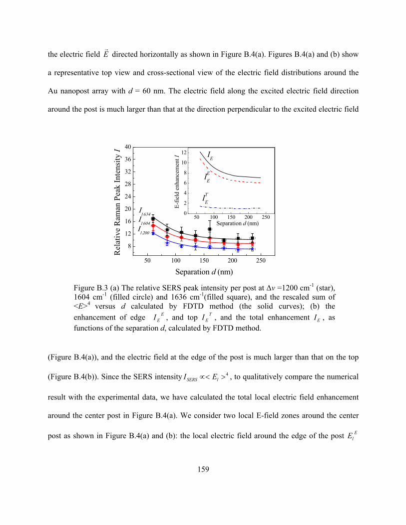
159
the electric field Er
directed horizontally as shown in Figure B.4(a). Figures B.4(a) and (b) show
a representative top view and cross-sectional view of the electric field distributions around the
Au nanopost array with d = 60 nm. The electric field along the excited electric field direction
around the post is much larger than that at the direction perpendicular to the excited electric field
(Figure B.4(a)), and the electric field at the edge of the post is much larger than that on the top
(Figure B.4(b)). Since the SERS intensity 4>∝< lSERS EI , to qualitatively compare the numerical
result with the experimental data, we have calculated the total local electric field enhancement
around the center post in Figure B.4(a). We consider two local E-field zones around the center
post as shown in Figure B.4(a) and (b): the local electric field around the edge of the post ElE
50 100 150 200 250
8
12
16
20
24
28
32
36
40
50 100 150 200 2500
2
4
6
8
10
12
Ι1634
Ι
1604
Rel
ativ
e R
aman
Pea
k In
tens
ity I
Separation d (nm)
Ι1200
ITE
IE
IEE
E-fie
ld e
nhan
cem
ent I
Separation d (nm)
Figure B.3 (a) The relative SERS peak intensity per post at Δν =1200 cm-1 (star), 1604 cm-1 (filled circle) and 1636 cm-1(filled square), and the rescaled sum of <E>4 versus d calculated by FDTD method (the solid curves); (b) the enhancement of edge E
EI , and top TEI , and the total enhancement EI , as
functions of the separation d, calculated by FDTD method.

160
and the local E-field on the top of the post ElE . The cylindrical part around the post (black
dashed lines in Figure B.4(b)) is used to calculate the enhancement due to the edge,
dvEI El
El
4
∫ ><= , and the top disk (white dashed rectangular in Figure B.4(b)) is used to
calculate the enhancement due to the top, dvEI Tl
Tl
4
∫ ><= . The thickness of the cylinder or the
disk is 9 nm for the calculation. The total enhancement is EE
TEE III += . Figure B.3(b) shows
the relative relationship among EI , EEI , and T
EI . With the increment of d, the field enhancement
on the top of the nanopost remains a constant, while the enhancement from the edge decrease
rapidly, and EEI is above 10 times of T
EI . The total enhancement EI calculated by FDTD can be
rescaled to fit the experimental data, as shown by the solid curves in Figure B.4(a). All the
(a) 0 V/m 2.586 V/m
E k
(b)
E k
0 V/m 2.950 V/m
Figure B.4 (a) The top view and (b) the cross-sectional view of the local E-field distribution of the 3×3 nanopost array calculated by FDTD method.

161
Raman intensities at the three different modes Δν = 1200 cm-1,1604 cm-1,and 1634 cm-1, agree
well with the numerical data, which demonstrates that in nanopost array, the separation of two
neighboring posts play a very important role for SERS enhancement. The agreement between the
experimental data and the numerical calculation attests the physical explanation by Gunnarsson
et al that the SERS intensity of a nanopost array is mainly from the contribution of the edge of
the posts and coupling effect, but the enhancement from the top of the post cannot be ignored.
B.4 Conclusions
Therefore, for a large separation, both experimental results and theoretical calculations
show that the coupling effect still plays a significant role in SERS EF. Although most SERS
signals come from the contribution of the edge of Au nano-post, the contribution from the top
cannot be ignored.

162
APPENDIX C
SHAPE DEPENDENCE OF SERS FROM GOLD NANOROD ARRAY
AND NANOCOMB ARRAY
From chapter 3, we found that the SERS intensity obtained from a Ag nanorod array
deposited onto a 500 nm Ag underlayer film is approximately 103 × more intense than that
obtained from a Ag nanorod array deposited directly onto a glass substrate [132, 174]. In order to
systematically explore the role of the underlayer film, we have prepared Au nanorod arrays and
Au nanocomb arrays by electron beam lithography (EBL), and compared the SERS response of
these two structures experimentally and theoretically. Our results show that both the Au
nanocomb and Au nanorod arrays exhibit similar SERS polarization dependence. The
normalized SERS intensity obtained from Au nanocomb arrays is larger than that obtained from
Au nanorod arrays. These SERS characteristics can be explained qualitatively by the local
electric field distribution calculated by a three-dimensional finite-difference time-domain (3D-
FDTD) method.

163
Figure C.1 shows SEM images of the Au nanorod arrays (Figure C.1(a)) and the Au
nanocomb arrays (Figure C.1(b)) fabricated by EBL. For the Au nanorod array (Figure C.1(a)),
the width of a nanorod is w = 107 ± 5 nm, the length l = 878 ± 4 nm, the edge-to-edge separation
between two neighboring nanorods in the x direction d = 165 ± 5 nm, and the separation between
two parallel lines of nanorods in the y direction D = 1 μm. For the Au nanocomb array (Figure
C.1(b)), the teeth of the nanocomb have the same structural parameters as those of the nanorod
array, while the spine of the nanocomb has a width t = 104 ± 6 nm in the y direction and a length
L = 0.5 mm in the x direction. The thickness of Au for both structures is 50 nm. These
parameters used in the EBL fabrication are based on the experimental data obtained from Ag
nanorod arrays prepared by OAD in our previous SERS studies [37].
(a) (b)
x
y
o x
y
o
D
d
1μm
Figure C.1 Top view SEM images of (a) Au nanorod array and (b) Au nanocomb array.
C.1 Fabrication and morphology of Au nanorod array and nanocomb array

164
SERS spectra were acquired using a Renishaw inVia Reflex Raman microscope system
(Renishaw, Hoffman Estates, IL) with elliptically polarized λ = 785 nm beam and linearly
polarized (extinction ratio > 500 : 1) λ = 633 nm beam. For λ = 633 nm excitation, the
polarization direction parallel to x- and y- axis of Au nano-rod (or the teeth of nanocomb) is
defined as s- and p-polarization, respectively. SERS spectra were collected at both wavelengths
using 50× magnification objective (laser spot size 28 μm2), 0.56 mW power, and 30 s collection
time. Samples were prepared by placing 1 μL of 10-4 M aqueous malachite green isothiocyanate
(MGITC) solution onto the Au nanostructure surfaces.
Figure C.2 shows the baseline corrected SERS spectra of MGITC collected with λ = 785
nm and λ = 633 nm with s- and p-polarizations for the Au nanorod arrays (Figure C.2(a)) and the
Au nanocomb arrays (Figure C.2(b)). The SERS intensity from both substrates at λ = 785 nm is
smaller than those at λ = 633 nm. This is likely due to a resonance contribution to the SERS
spectrum from MGITC, as it has an electronic absorbance at λ = 633 nm [10, 202]. For both
1125 1250 1375 1500 16250
10k
20k
30k
40k
Ram
an In
tens
ity (c
ount
s)
Raman Shift (cm-1)
633 nm s-polarization excitation 633 nm p-polarization excitation 785 nm excitation
(a) Nanorod
1125 1250 1375 1500 1625
Raman Shift (cm-1)
633 nm s-polarization excitation 633 nm p-polarization excitation 785 nm excitation
(b) Nanocomb
Figure C.2 Representative SERS spectra of MGITC obtained from (a) Au nanorod array and (b) Au nanocomb array at λ = 785 nm, and under s-polarization and p-polarization at λ = 633 nm.
C. 2 SERS characterization and comparison of nanorod and nanocomb

165
substrates, the SERS signals excited by s-polarization are stronger than that excited by p-
polarization. In addition, the SERS intensity obtained from the Au nanocomb array is stronger
than that obtained from Au nanorod array. One of the reasons for this result may be that exposed
Au surface area of Au nanocomb (11.96 μm2) is larger than that of Au nanorods (10.18 μm2) Au
surface due to the extra spine in the structure. Assuming that the MGITC molecules are
uniformly spread on all the Au surfaces, the area normalized integrated intensity of the band at
1173 cm-1 for the in-plane C-H bend of MGITC can be used to make quantitative comparisons.
We denote the normalized Raman peak intensities excited by s-polarization, p-polarization of λ =
633 nm and λ = 785 nm as ScombI 633 , P
combI 633 and 785combI for the Au nanocomb array, and S
rodI 633 , ProdI 633 and
785rodI for the Au nanorod array, respectively. The ratios of the normalized Raman intensity under
different configurations can be estimated and are shown in Table C.1. For the same nanostructure,
the ratios of the normalized SERS intensity by p-polarization λ = 633 nm excitation over λ = 785
nm excitation are almost the same: 5.01.4/ 785633 ±=combP
comb II , and 4.09.4/ 785633 ±=rodP
rod II . The ratio
of s-polarization over p-polarization excitation at λ = 633 nm, 7.08.1/ 633633 ±=Pcomb
Scomb II and
4.05.2/ 633633 ±=Prod
Srod II , are larger than 1 for both the Au nanorod array and the Au nanocomb
array. We note that the polarized intensity ratio for the Au nanocomb array (1.8) is smaller than
Table C.1 The ratio of experimental SRES intensity and the normalized overall local field enhancement ratio rodcomb II '/' at different detection configuration for different nanostructures.
785633 / combP
comb II 785633 / rodP
rod II Pcomb
Scomb II 633633 / P
rodS
rod II 633633 / Prod
Pcomb II 633633 / 785785 / rodcomb II
Experimental 4.1 ± 0.5 4.9 ± 0.4 1.8 ± 0.7 2.5 ± 0.4 3.7 ± 0.4 4.4 ± 0.7
3D-FDTD 0.6 0.6 1.6 2.4 1.4 1.4

166
that for the Au nanorod array (2.5). This could be due to two reasons: the structural anisotropy of
the array, in which the spine of the comb structure breaks the symmetry of the rod array, making
the comb structure less anisotropic compared to the rod array; and a potential coupling effect
between the teeth and the spine for the Au nanocomb array in p-polarized excitation, resulting in
a stronger Raman intensity for the Au nanocomb array compared to the nanorod array.
We also find that the normalized Raman intensity obtained from a Au nanocomb array is
always larger than that from a Au nanorod array, regardless of the excitation wavelength:
7.04.4/ 785785 ±=rodcomb II , 8.00.3/ 633633 ±=Srod
Scomb II and 4.07.3/ 633633 ±=P
rodP
comb II . These ratios are very
similar when the experimental error is taken into account, which shows that underlying spine of
the Au nanocomb array significantly improves the SERS enhancement. This result is
qualitatively consistent with our previous observation for Ag nanorod array substrates [132].
C.3 Theoretical explanation by FDTD method
To understand those experimental results, we have calculated the local electric field
distributions lEr
excited at λ = 785 nm and λ = 633 nm under different polarization
configurations using the 3D-FDTD method. A 1 × 5 array of Au nanorods and nanocomb with a
width w = 100 nm, d = 175 nm, l = 900 nm, and t = 100 nm were used in these calculations.
Figure C.3 shows the E-field distributions around Au nanostructures excited at λ = 633 nm. For
a nanorod array under p-polarization excitation (Figure C.3(a)), it appears that the electric fields
at the ends of the nanorod are much stronger than that around the side walls of the nanorod;
while under s-polarization excitation (Figure C.3(b)), the electric fields around the side wall of

167
the nanorod is stronger than that at the tips of the nanorod. For a nanocomb array under p-
polarization excitation (Figure C.3(c)), the strongest E-field is located at the top surface of the
teeth and the intersection corners between the teeth and spine; while under s-polarized excitation
(Figure C.3(d)), the strongest E-field is along the side wall of the nanocomb teeth.
The normalized SERS intensity is not only determined by the local E-field,
4>∝< lSERS EI , but also by the local surface density of Raman probe molecules n, as well as the
resonant Raman enhancement factor rG [203, 204]: ∫∫∫∫= dAdAnEGCI lrSERS /4 , where C is a
constant that may depend on specific nanostructures, and the integration is performed throughout
E k
(a) (b)
(c) (d)
E k
E
k ①
①
②
②
③
E k ①
①
②
②
③
Figure C.3 The local E-field distribution excited at λ = 633 nm for p-polarization (a) and s-polarization (b) of Au nanorod array, and for p-polarization (c) and s-polarization (d) of Au nanocomb array. The dashed squares in (a) and (c) show different surfaces of the two nanostructures: ① end surface; ② side surface; ③ top surface.

168
all the exposed Au surfaces. Under the assumption that the Raman molecules are uniformly
adsorbed on the Au surfaces, and rG only depends on the excitation wavelength, the normalized
SERS intensity can be rewritten as,
∫∫∫∫= dAdAEnCGI lrSERS4 . (C.1)
The normalized local electric field enhancements ∫∫∫∫= dAdAEI l4' for different surfaces
shown in Figure C.3 are calculated, and the ratios rodcomb II '/' for different surfaces are listed in
Table C.2. Under most conditions, the field enhancement for nanocomb is larger than that of
nanorod, especially at the top and side surfaces, which count for more than 88% and 94% of the
total surface areas of nanocomb and nanorod structures. Thus, the addition of the nano-spine
significantly increases the local E-field around all surfaces.
To compare with the experimental results, the ratios of the normalized local electric field
enhancement from all the surfaces for different excitation wavelengths and polarizations for
nanocomb and nanorod structures are calculated and listed in Table C.2. The polarization ratios,
4.2'' 633633 =Prod
Srod II and 6.1'' 633633 =P
combS
comb II , agree very well with the experimental values (2.5 ±
0.4 and 1.8 ± 0.7). This is expected that for the same structure and excitation wavelength the
parameters C, n, and rG are the same, and according to equation (C.1), the SERS intensity ratios
only depend on the ratios of I'. For the same structure but excited with different wavelength, the
ratios 6.0'/' 785633 =combP
comb II and 6.0'/' 785633 =rodP
rod II are the same. These ratios are much smaller than
experimental values 5.01.4/ 785633 ±=combP
comb II , and 4.09.4/ 785633 ±=rodP
rod II . According to equation
(C.1), 785785633633785633 '/'/ IGIGII rrP = , the discrepancy comes from the ratio of resonant

169
enhancement factor 785633 / rr GG . Due to the resonance absorbance of MGITC molecules at λ =
633 nm, 785633rr GG > . We obtain that 2.87.6/ 785633 −=rr GG , i.e., the resonant absorbance at λ =
633 nm can generate 7-8 times higher Raman signal than that of λ = 785 nm. This small ratio of
785633 / rr GG is much lower than the enhancement (100 ~ 1000) due to surface enhanced Resonant
Raman scattering (SERRS) compared to SERS [205, 206].
The E-field enhancement ratios for different structures under the same detection
configuration, 4.1'/' 633633 =Prod
Pcomb II , and 4.1'/' 785785 =rodcomb II , predict that the SERS signal from
nanocomb structure should be always larger than that of the nanorod structure, qualitatively
agreed with the experiments. It also shows that the ratio rodcomb II '/' is independent on the
detection configuration, i.e., the wavelength and polarization, as demonstrated by the
experiments. However, the ratio rodcomb II '/' is about 3 times less than the experimental value of
rodcomb II / . According to equation (C.1), rodrodcombcombrodcomb ICICII '/'/ = , and this implies that
the constant C depends on the detailed nanostructure. From both the experimental and theoretical
Table C.2 The ratio of normalized local field enhancement ratio rodcomb II '/' at different detection configuration for different surfaces of the nanostructures.
Top Surfaces Side Surfaces End Surfaces
λ = 633 nm p-polarization 1.34 1.33 0.45
s-polarization 1.07 0.90 1.10
λ = 785 nm p-polarization 1.21 1.66 0.98
s-polarization 1.52 1.04 1.40

170
data, we obtain that 1.36.2/ −≈rodcomb CC . This non-unity rodcomb CC / ratio could be due to
the detailed molecular orientation and E-field direction on different surfaces for different
structures, or the effect from Si substrates.

171
APPENDIX D
FINITE DIFFERENCE TIME DOMAIN NUMERICAL METHOD
Generally, the nanoparticle systems are too complicated to directly get an analytical
solution for the local electric field over nanoparticles. numerical methods have often been
borrowed to calculate the local electric distribution such as multiple multipole approximation
(MMP) [84-86], discrete dipole approximation (DDA) [87-89], and finite difference time domain
(FDTD) methods [90-95].
Compared to other numerical methods, the FDTD method can be applied to various
complex problems such as large particles and particles array with any shapes and so on, and one
time propagation can provide information about a wide range of frequencies. In addition, in
demanding of computation, the core algorithm is sufficiently simple and can be efficiently
implemented on parallel computers [207]. FDTD method was first time and completely
developed by K. S. Yee in 1966 [95]. It is a time-propagation algorithm numerical method for
solving differential Maxwell’s equations, which are discretized using central-difference
approximations to space and time partial derivatives. For a metallic nanostructure, the general
form of differential Maxwell’s equations can be given by
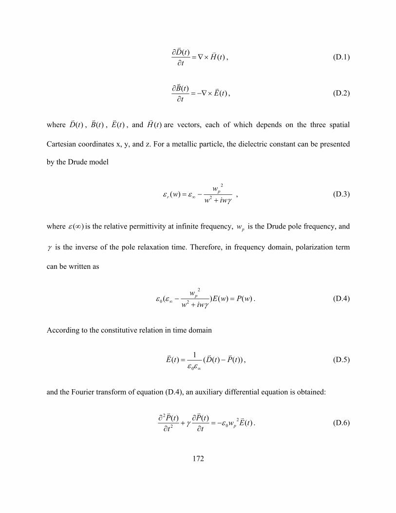
172
)()( tHttD v
v
×∇=∂
∂ , (D.1)
)()( tEttB v
v
×−∇=∂
∂ , (D.2)
where )(tDv
, )(tBv
, )(tEv
, and )(tHv
are vectors, each of which depends on the three spatial
Cartesian coordinates x, y, and z. For a metallic particle, the dielectric constant can be presented
by the Drude model
γεε
iwww
w pr +
−= ∞ 2
2
)( , (D.3)
where )(∞ε is the relative permittivity at infinite frequency, pw is the Drude pole frequency, and
γ is the inverse of the pole relaxation time. Therefore, in frequency domain, polarization term
can be written as
)()()( 2
2
0 wPwEiww
wp =+
−∞ γεε . (D.4)
According to the constitutive relation in time domain
))()((1)(0
tPtDtEvvv
−=∞εε
, (D.5)
and the Fourier transform of equation (D.4), an auxiliary differential equation is obtained:
)()()( 202
2
tEwttP
ttP
p
vvv
εγ −=∂
∂+
∂∂ . (D.6)
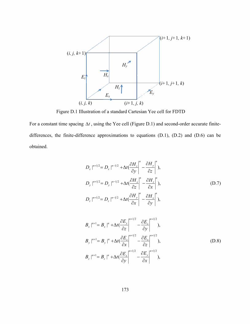
173
For a constant time spacing tΔ , using the Yee cell (Figure D.1) and second-order accurate finite-
differences, the finite-difference approximations to equations (D.1), (D.2) and (D.6) can be
obtained.
),(||
),(||
),(||
2121
2121
2121
n
x
nyn
zn
z
nz
nxn
yn
y
ny
n
znx
nx
yH
xH
tDD
xH
zHtDD
zH
yHtDD
∂∂
−∂
∂Δ+=
∂∂
−∂
∂Δ+=
∂∂
−∂
∂Δ+=
−+
−+
−+
(D.7)
),(||
),(||
),(||
21211
21211
21211
+++
+++
+++
∂∂
−∂
∂Δ+=
∂∂
−∂
∂Δ+=
∂∂
−∂
∂Δ+=
ny
n
xnz
nz
nx
nzn
yn
y
n
z
nyn
xn
x
xE
yEtBB
zE
xEtBB
yE
zE
tBB
(D.8)
Ez
Ex Ey
Hz
Hx
Hy
(i, j, k)
(i, j, k+1)
(i+1, j, k)
(i+1, j+1, k)
(i+1, j+1, k+1)
Figure D.1 Illustration of a standard Cartesian Yee cell for FDTD

174
))2/1
(|)2/12/1(|)
2/12(| 21
220232121 −−−+
Δ+Δ
−Δ+Δ−
−Δ+
= npnnn Et
twP
ttP
tP
γε
γγ
γ. (D.9)
During the solving of the above equations, an initial wavepacket, which represents the plane
wave incident on the particle, is required. In the mean time, boundary conditions are used on the
edge of the grid to avoid unphysical reflections. Generally, absorbing boundary condition is
applied in the calculations, but this boundary condition is not practical for three-dimensional
simulations. Berenger’s perfectly matched layer (PML) boundary has been proven to be a good
approach in three dimensional problems. Then the time-dependent electric field can be calculated
out according to above equations. In order to estimate the SERS EF, the frequency-resolved
electric field is usually employed, therefore, the Fourier transformation should be performed for
the time-domain electric field.