Optimising the fabrication of organic light-emitting diodes by laser-induced forward transfer

IEEE JOURNAL ON SELECTED TOPICS IN QUANTUM ELECTRONICS, VOL. 6, NO. 6, NOVEMBER/DECEMBER 2000 1201
Surface-Emitting Laser—Its Birth and Generation ofNew Optoelectronics Field
Kenichi Iga, Fellow, IEEE
Invited Paper
Abstract—The surface-emitting laser (SEL) is considered oneof the most important devices for optical interconnects and LANs,enabling ultra parallel information transmission in lightwave andcomputer systems. In this paper, we will introduce its history, fabri-cation technology, and discuss the advantages. Then, we review theprogress of the surface-emitting laser and the vertical-cavity sur-face-emitting laser (VCSEL), covering the spectral band from in-frared to ultraviolet by featuring its physics, materials, fabricationtechnology, and performances, such as threshold, output powers,polarizations, line-width, modulation, reliability, and so on.
Index Terms—DBR, distributed Bragg reflector, gigabit eth-ernet, LAN, laser array, microlaser, microlens, multilayer, paralleltransmission, quantum well, semiconductor laser, surface-emit-ting laser, vertical cavity laser, vertical-cavity surface-emittinglaser.
I. INTRODUCTION
WHAT IS THE surface-emitting laser (SEL) or the verticalcavity surface-emitting laser (VCSEL)? The structure is
substantially different from conventional stripe lasers, i.e., thevertical cavity is formed by the surfaces of epitaxial layers andlight output is taken from one of the mirror surfaces as shownin Fig. 1(a).
VCSEL [1], [2] looked to meet the third generation of devel-opment in 1999, as seen from Table I, as we entered a new infor-mation and technology era in 2000. The VCSEL is being appliedin various optical systems, such as optical networks, parallel op-tical interconnects, laser printers, high density optical disks, andso on. We review its history and the progress of VCSELs in widespectral ranges covered by variousIII –V compound semicon-ductors. Recent technologies and future prospects will be dis-cussed.
We summarized the brief history of VCSEL research inTable I. It is recognized that the author suggested the deviceof VCSEL in 1977, as shown in Fig. 1(b). The first devicecame out in 1979, where we used a 1300-nm wavelengthGaInAsP–InP material for the active region [3]. In 1986, wemade a 6-mA threshold GaAs device [4] and then employedthe metal organic chemical vapor deposition (MOCVD). The
Manuscript received July 13, 2000. This work was supported by the Min-istry of Education, Science, Sport, and Culture with a Grant from COE Program07CE2003.
The author is with the P&I Microsystem Research Center, Tokyo Institute ofTechnology, 4259 Nagatsuta, Midoriku, Yokohama 226-8503, Japan.
Publisher Item Identifier S 1077-260X(00)11545-X.
(a)
(b)
Fig. 1. Model of VCSEL. (a) Current model. (b) Initial idea.
first room-temperature continuous-wave (CW) device usingGaAs material was demonstrated in 1988 [5]. In 1989, Jewelldemonstrated a GaInAs VCSEL exhibiting a 1–2-mA threshold[6]. These two experiments encouraged the audience to begetting up at the stage of vertical-cavity surface-emitting laserresearch. Submilliampere threshold devices were demonstrated
1077–260X/00$10.00 © 2000 IEEE

1202 IEEE JOURNAL ON SELECTED TOPICS IN QUANTUM ELECTRONICS, VOL. 6, NO. 6, NOVEMBER/DECEMBER 2000
TABLE IHISTORY OFVCSEL RESEARCH
by improving the active region and distributed Bragg reflectors(DBRs).
Since 1992, VCSELs based on GaAs have been extensivelystudied [7]–[9] and some 780, 850, and 980-nm devices are nowcommercialized into optical systems. We improved a 1500-nmVCSEL [10] demonstrated a 1300-nm room-temperature CWdevice [11]. A wafer fusion technique enabled us to operate1550-nm VCSELs at higher temperatures [12]. In 1993, a room-temperature high-performance CW red AlGaInAs device wasdemonstrated [13]. Since 1996, green-blue-ultraviolet device re-search was started [14], [15]. Since 1999, VCSEL-based opticaltransmitters have been introduced into gigabit per second LANs.
The initial motivation of SEL invention was a fully mono-lithic fabrication of laser cavity. Based upon this concept, thecurrent issues include high speed modulation capability at verylow-power consumption level, reproducible array production,and inexpensive moduling.
The VCSEL structure may provide a number of advantagesas follows:
1) ultralow threshold operation is expected from its smallcavity volume, reaching microampere levels;
2) is possible, where drivingcurrent and threshold current;
3) wavelength and thresholds are relatively insensitiveagainst temperature variation;
4) dynamic single-mode operation is possible;5) large relaxation frequency provides high-speed modula-
tion capability;6) long device lifetime is due to completely embedded ac-
tive region and passivated surfaces;7) high-power conversion efficiency, i.e., %;8) vertical emission from substrate;9) easy coupling to optical fibers due to good mode
matching from single mode through thick multimodefibers;
10) a number of laser devices can be fabricated by fullymonolithic processes yielding very low cost chip pro-duction;
11) the initial probe test can be performed before separatingdevices into discrete chips;
12) easy bonding and mounting;13) cheap modules and package cost;14) densely packed and precisely arranged two-dimensional
(2-D) laser arrays can be formed;15) vertical stack integration of multithin-film functional op-
tical devices can be made intact to the VCSEL resonator,taking the advantage of micromachining technology andproviding polarization independent characteristics;
16) compatible integration together with LSIs.
In this paper, we would like to review the progress of VCSELsin a wide range of optical spectra based on GaInAsP, AlGaInAs,GaInNAs, GaInAs, GaAlAs, AlGaInP, ZnSe, GaInN, and othermaterials.
II. BASICS OFVCSEL
A. Threshold Current
The physical difference between VCSELs and conventionalstripe geometry lasers is summarized in Table II. The majorpoints are that the cavity length of VCSELs is in the order ofwavelength which is much smaller than that of stripe lasers,having about a 300-m wavelength and several micrometersof lateral size. Those provide us with substantial differences inlaser performances.
We would like to discuss the threshold current of VCSELs.The threshold current of SELs can be expressed by the equa-tion with threshold current density
(1)
where is electron charge. is the volume of active region,which is given by
(2)
The threshold carrier density is given by
(3)
The parameters used are defined as follows, whereabsorption loss coefficient averaged per unit length;diffraction loss coefficient averaged per unit length;mirror loss coefficient;gain coefficient expressing differential gain
, with as the optical gain per centimeters;effective recombination coefficient;total active layer thickness;diameter of active region;effective cavity length, including spacing layers andpenetration layers of Bragg reflectors;transparent carrier density;photon lifetime in cavity;recombination lifetime;optical energy confinement factor, ;transverse confinement factor;longitudinal confinement factor or filling factor rel-ative to stripe lasers (for thick active layer)
(for thin active layer, which is located atthe loop of optical standing wave);injection efficiency, sometimes referred as internalefficiency;spontaneous emission efficiency.
As seen in (1), we recognize that it is essential to reduce thevolume of active region in order to decrease the threshold cur-rent. Assume that the threshold carrier density does not changethat much. If we reduce the active volume, we can decrease thethreshold as we make a small active region. We compare the di-mensions of surface-emitting lasers and conventional stripe ge-

IGA: SURFACE-EMITTING LASER—ITS BIRTH AND GENERATION OF NEW OPTOELECTRONICS FIELD 1203
TABLE IICOMPARISON OFPARAMETERS BETWEEN STRIPE LASER AND VCSEL
ometry lasers in Table II. Notice that the volume of VCSELscould be m , whereas the stripe lasers remain
m . This directly reflects the threshold current: thetypical threshold of stripe lasers ranges from microampere orhigher, while that for VCSEL is less than microampere due toa simple carrier confinement scheme, such as proton bombard-ment. It could even be as low as microampere by implementingsophisticated carrier and optical confinement structures, as willbe introduced later.
An early stage estimation of threshold showed that thethreshold current can be reduced in proportion to the squareof the active region diameter. However, there should be aminimum value originating from the decrease of optical con-finement factor that is defined by the overlap of optical modefield and gain region when the diameter is becoming small. Inaddition, the extreme minimization of volume, in particular, inthe lateral direction, is limited by the optical and carrier lossesdue to optical scattering, diffraction of lightwave, nonradiativecarrier recombination, and other technical imperfections.
B. Output Power and Quantum Efficiency
Also, we discuss the differential quantum efficiency of theVCSEL. If we use a nonabsorbing mirror for the front reflector,the differential quantum efficiency from the front mirror isexpressed as
(4)
where is the total internal loss and andare front and rear mirror reflectivities.
The optical power output is expressed by
(5)
whereis bandgap energy;is spontaneous emission factor;is driving current.
On the other hand the power conversion efficiencyfar abovethreshold is given by
(6)
where is bias voltage and the spontaneous componenthas been neglected. In the case of surface-emitting laser, thethreshold current could be very small and therefore, the powerconversion efficiency can be relatively large, i.e., higher than50%. The power conversion efficiency is sometimes calledwall-plug efficiency.
The modulation bandwidth is given by
(7)
where denotes the relaxation frequency, which is expressedby the equation
(8)
The photon lifetime is given by
(9)
The photon lifetime is normally in the order of psec, whichcan be made slightly smaller than stripe lasers. Since thethreshold current can be very small in VCSELs, the relaxationfrequency could be relatively higher than the stripe lasers evenin low driving ranges. The threshold carrier density can

1204 IEEE JOURNAL ON SELECTED TOPICS IN QUANTUM ELECTRONICS, VOL. 6, NO. 6, NOVEMBER/DECEMBER 2000
be expressed in terms of photon lifetime, which represents thecavity loss and given by using (3) and (9);
(10)
It is noted that the threshold carrier density can be small if wemake the differential gain , the confinement factor, andthe photon lifetime large.
C. Criteria for Confirmation of Lasing
When we face a new or ultralow threshold device to checkthe lasing operation, the existence of a break from the linearincrease of light output versus injection current (– ) charac-teristic is an easy observation. Sometimes a nonlinearity is ob-served in the – characteristic but this does not necessarilymean laser oscillation. Even with a nonlasing sample nonlin-earity is owed to the “filtering effect,” electron-hole plasmaemission, and nonradiating floor. The methods used to confirmthe laser operation of vertical cavity, for example, are as follows:
1) break or kink in ( – ) characteristic;2) narrow spectral linewidth Å;3) difference of near field pattern (NFP) and far field pat-
tern (FFP) between the emissions below and above thethreshold;
4) linearly polarized light of the emission above thethreshold.
III. D EVICE DESIGN AND MATERIAL
A. Device Configuration
As already shown in Fig. 1(a), the structure common to mostVCSELs consists of two parallel reflectors, which sandwich athin active layer. The reflectivity necessary to reach the lasingthreshold normally should be higher than 99.9%. Together withthe optical cavity formation, the scheme for injecting electronsand holes effectively into a small volume of active region is nec-essary for the current injection device. The ultimate thresholdcurrent depends on how to make the active volume small, as in-troduced in the previous section, and how well the optical fieldcan be confined within the cavity to maximize the overlap withactive region. These confinement structures will be presented inthe later sections.
B. Materials
We show some material choices for VCSELs in Fig. 2. We listproblems below that should be considered when making VC-SELs, as discussed in the previous section:
1) design of resonant cavity and mode-gain matching;2) multilayered DBRs to realize high reflective mirrors;3) optical losses such as Auger recombination, intervalence
band absorption, scattering loss, and diffraction loss;4) p-type doping to reduce the resistivity in p-type materials
for CW and high efficiency operation (if we wish to formmultilayer DBRs, this will become much more severe);
5) heat sinking for high-temperature and high-power opera-tion;
Fig. 2. Materials for VCSELs in wide spectral bands.
Fig. 3. Structures for current confinement.
6) catastrophic optical damage (COD) level is very impor-tant for high power operation;
7) crystal growth at reasonably high temperatures (e.g.,higher than half of the melting temperatures).
C. Current Injection Scheme
Let us consider the current confinement for VCSELs. InFig. 3, we show typical models of current confinement schemesreported so far.
a) Ring or circular electrode type: This structure can limitthe current flow in the vicinity of the ring electrode. Thelight output can be taken out from the center window. Thisis easy to fabricate, but the current can not be confinedcompletely within a small area due to diffusion.
b) Proton bombardment type: We make an insulating layerby proton (H ) irradiation to limit the current spreadingtoward the surrounding area. The process is rather simple,and most of commercialized devices are made by thismethod.
c) Buried heterostructure (BH) type: We bury the mesa, in-cluding the active region, with a wide-gap semiconductor

IGA: SURFACE-EMITTING LASER—ITS BIRTH AND GENERATION OF NEW OPTOELECTRONICS FIELD 1205
Fig. 4. Structures for optical confinement.
to limit the current. The refractive index can be small inthe surrounding region, resulting in the formation of anindex-guiding structure. This is an ideal structure in termsof current and optical confinement. The problem is thatthe necessary process is rather complicated, particularly,in making a tiny three-dimensional (3-D) device.
d) Air-post type: The circular or rectangular air-post is usedto make a current confinement. This is the simplest wayfor device fabrication, although nonradiative recombina-tion at the outer wall may deteriorate the performance.
e) Selective AlAs oxidation type: We oxidize the AlAs layerto make a transparent insulator.
f) Oxidized DBR type: The same method as above is appliedto oxidize DBR, consisting of AlAs and GaAs. This isonly one volume confinement method that can reduce thenonradiative recombination.
By developing new process technology, we could reach thelaser performance, which is expected from the theoretical con-sideration.
D. Optical Guiding
The optical confinement schemes developed for VCSELs areintroduced in Fig. 4. The fundamental concept is to increase theoverlap of optical field with gain region.
a) Fabry–Perot type: The optical resonant field is determinedby the two reflectors forming the plane that is parallel tothe Fabry–Perot resonator. The diffraction loss increasesif the mirror diameter gets too small.
b) Gain-guide type: We simply limit the field at the regionwhere the gain exists. The mode may be changed at higherinjection levels due to spatial hole burning.
c) BH: As introduced in the previous section, an ideal indexguiding can be formed.
d) Selective AlAs oxidation type: Due to the index differencebetween AlAs and the oxidized region, we can confine theoptical field as well by a lens effect.
e) Antiguiding type: The index is designed to be lower in thesurrounding region in order to make a so-called antigu-iding scheme. The threshold is rather high, but this struc-ture is good for stable mode in high driving levels.
E. Transverse and Longitudinal Mode
The resonant mode in most SELs can be expressed by thewell known Fabry–Perot TEM mode. The NFP of fundamentalmode can be given by the Gaussian function
(11)
whereoptical field;lateral distance;denotes spotsize.
The spotsize of normal SELs is several micronmeters, andrelatively large when compared with stripe lasers, i.e., 2–3m.In the case of multimode operation, the mode behaves like thecombination of multiple TEM . The associated spectrum isbroadened due to different resonant wavelengths.
FFP associated with Gaussian near field can be expressed byGaussian function; spreading angle is given by
(12)
Here, if m and m, then (rad) .This kind of angle is narrower than conventional stripe lasers.
F. Polarization Mode
The VCSEL generally has linear polarization without excep-tion. This is due to a small amount of asymmetric loss comingfrom the shape of the device or material. The device grown on a(100)-oriented substrate polarizes in (110) or equivalent orien-tations. The direction can not be identified definitely, and some-times switches over due to spatial hole burning or temperaturevariation. In order to stabilize the polarization mode, specialcare should be taken. This issue will be discussed later.
IV. SURFACE-EMITTING LASER IN LONG-WAVELENGTH BAND
A. GaInAsP–InP VCSEL
The first SEL device was demonstrated by usingGaInAsP–InP system in 1978 and published in 1979 [3].The importance of 1300- or 1550-nm devices is currentlyincreasing because parallel lightwave systems are really neededto meet rapid increase of information transmission capacity inLANs. However, the GaInAsP–InP system, which is conven-tionally used in trank communication systems with the helpof temperature controller, has some substantial difficulties formaking VCSELs due to the following reasons.
1) Auger recombination and inter-valence band absorption(IVBA) are noticeable.
2) Index difference between GaInAsP and InP is relativelysmall to make DBR mirrors.
3) Conduction band offset is small.

1206 IEEE JOURNAL ON SELECTED TOPICS IN QUANTUM ELECTRONICS, VOL. 6, NO. 6, NOVEMBER/DECEMBER 2000
Fig. 5. 1300-nm VCSELs with thermally conductive dielectric DBR.
Two hybrid mirror technologies are being developed. Oneuses a semiconductor/dielectric reflector [10]. Thermal prob-lems for CW operation are extensively studied. A MgO–Simirror with good thermal conductivity was demonstrated andachieved the first room-temperature CW operation with 1300nm surface-emitting lasers, as shown in Fig. 5 [11]. Betterresults have been obtained by using AlO –Si mirrors [16].
The other is an epitaxial bonding of GaInAsP–InP active re-gion and GaAs–AlAs mirrors, where a 144C pulsed opera-tion was achieved by optical pumping. The AlAs–GaAs mirrorhas advantages in both electrical and thermal conductivity. CWthreshold of 0.8 mA [17] and maximum operating temperatureof up to 69 C [12] have been reported for 1550-nm VCSELswith double-bonded mirrors [17]. More recently, the maximumoperation was achieved at 71C [18]. In 1998, a tandem struc-ture of 1300-nm VCSEL optically pumped by a 850-nm VCSELhas been demonstrated to achieve 1.5 mW of output power [19].However, the cost of wafer consumption in wafer fusion devicesmay become the final bottleneck of low-cost commercialization.
Recently, a GaAsSb QW on GaAs substrate has beendemonstrated for the purpose of 1300-nm VCSELs [20]. AnAlGaAsSb–GaAs system has been found to form a good DBR[21]. Tunnel junction and AlAs oxide confinement structuresmay be very helpful for long-wavelength VCSEL innovation[22].
B. AlGaInAs–AlGaInAs VCSEL
The AlGaInAs lattice matched to InP is also considered. Thissystem may exhibit a larger conduction band offset than the con-ventional GaInAsP system. Moreover, we can grow a thin AlAslayer to make the native oxide for a current confining aperturelike the GaAs–AlAs system. The preliminary study has beenmade to demonstrate a stripe laser in our group, where a large
was demonstrated. By using this system, the first monolithicVCSEL was fabricated, demonstrating room-temperature CWoperation [23].
C. Long Wavelength VCSELs on GaAs Substrate
Another interesting system is GaInNAs lattice-matched toGaAs, as is shown in Fig. 6. This system has been pioneeredby Kondowet al. [24] with a gas-source molecular-beam epi-taxy (GSMBE). Also, -nm stripe lasers were fabri-cated, where the nitrogen content is 0.4%. Room-temperatureCW operation of horizontal cavity lasers recently has been ob-tained, exhibiting the threshold current density of 1.5 kA/cm.
Fig. 6. Bandgap versus lattice-constant diagram.
Also, stripe geometry lasers were demonstrated with a thresholdof 24 mA at room temperature [25]. It is reported that char-acteristic temperature is approximately 120K at room temper-ature [25]. If we can increase the nitrogen content up to 5%, thewavelength band of 1300–1550 nm may be covered. In partic-ular, GaAs–AlAs Bragg reflectors can be incorporated on thesame substrate, and AlAs oxidation is utilized [26]. Some con-sideration of device design was presented [27]. In any case, thissystem will substantially change the surface-emitting laser per-formances in the long wavelength range. Larsonet al.first real-ized a VCSEL using this system [28].
The long-wavelength VCSEL formable on GaAs, as shown inFig. 7 will have a great impact upon the realization of high per-formance devices. GaInNAs–GaAs is expected as a new mate-rial for long wavelength VCSELs. Every GaAs-based structurecan be applied, and a large conduction band offset is expected.Some 1300-nm edge emitting lasers and a 1186-nm VCSELswere demonstrated. We achieved a lasing operation in GaInNAsedge emitters grown by chemical beam epitaxy (CBE), demon-strating K [29]. The Ga In As ternary substratewill be viable to make a high performance laser device by in-corporating . Some sophisticated method to form thisternary substrate is attempted, growing [30].
During the research of GaInNAs lasers, we found that ahighly strained GaInAs–GaAs system containing large In-con-tent ( 40%) can provide an excellent temperature characteristic[31], i.e., operating with K [32]. This system shouldbe viable for -nm VCSELs for silica-fiber-basedhigh-speed LANs [33].
A quantum dot structure is considered as a long-wavelengthactive layer on a GaAs substrate. A 1150-nm GaInAs-dotVCSEL was reported with a threshold current of 0.5 mA [73].
V. SURFACEEMITTING LASER IN MIDWAVELENGTH BAND
A. 980-nm GaInAs–GaAs VCSEL
The GaInAs–GaAs strained pseudomorphic system grown ona GaAs substrate emitting 0.98m of wavelength exhibits ahigh laser gain and has been introduced into SELs together withGaAs–AlAs multilayer reflectors [34]. A low threshold (1 mAat CW) has been demonstrated by Jewellet al.[6]. The thresholdcurrent of VCSELs has been reduced to submilliampere ordersin various institutions of the world. Very low thresholds reported

IGA: SURFACE-EMITTING LASER—ITS BIRTH AND GENERATION OF NEW OPTOELECTRONICS FIELD 1207
Fig. 7. Choices of long wavelength VCSELs formable on GaAs substrate.
before 1995 are 0.7 mA [7], 0.65 mA [8], and0.2 mA [35].Moreover, a threshold of 91A at room-temperature CW op-eration was reported by introducing the oxide current and op-tical confinement [36]. The theoretical expectation is less than10 A, if some good current and optical confinement structurecan be introduced.
It has been made clear that the oxide aperture can functionas a focusing lens since the central window has a higher indexand the oxide region exhibits a lower index. This provide uswith some phase shift to focus the light toward the center axis,which reduces the diffraction loss. The Al-oxide is effectiveboth for current and optical confinements and solves the prob-lems on surface recombination of carriers and optical scattering.We demonstrated 70A [37], [38] of threshold by using oxideDBR structure, 40 A [39], and 8.5 A [40].
In 1995, we developed a novel laser structure employingselective oxidizing process applied to AlAs, which is onemember of the multilayer Bragg reflector. The schematicstructure of the device now developed is shown in Fig. 8(a)[37], [38]. The active region is three quantum wells consistingof 80 Å GaInAs strained layers. The Bragg reflector consistsof GaAs–AlAs quarter wavelength stacks of 24.5 pairs. Afteretching the epitaxial layers, including active layer and twoBragg reflectors, the sample was treated in a high-temperatureoven with water vapor that had been bubbled by nitrogen gas.The AlAs layers are oxidized, preferentially with this process,and native oxide of Aluminum is formed at the periphery ofetched mesas. It is recognized from SEM picture that only AlAslayers in DBR have been oxidized, as shown in Fig. 8(b) [41].The typical size is 20-m core starting from a 30-m mesadiameter. We have achieved about 1 mW of power output andsubmicroampere threshold. The nominal lasing wavelength is0.98 m. We have made a smaller diameter device having 5mstarted from 20 m mesa. The minimum threshold achievedis 70 A at room temperature CW operation [38] as shown inFig. 9. As the theoretically predicted, threshold is about 1Aand this record may soon be cleared.
A relatively high power higher than 50 mW is becoming pos-sible [42]. The power conversion efficiency 50% is reported.
(a)
(b)
Fig. 8. (a) Schematic structure of oxide-confined GaInAs–GaAs VCSEL. (b)Oxidized AlAs layers in DBR.
[43]. Also, high efficiency operation at relatively low drivinglevels, i.e., a few milliamperes, became possible, which has beenhard to achieve with stripe lasers. This is due to the availabilityof low resistive DBRs in corporation with Al-oxide aperture. Indevices of about 1 m in diameter, higher than 20% of powerconversion efficiencies were reported [44], [45].
Regarding the power capability, near 200 mW has beendemonstrated by a large size device in [46]. In a 2-D arrayinvolving 1000 VCSELs with active cooling, more than 2 W ofCW output was achieved [47].

1208 IEEE JOURNAL ON SELECTED TOPICS IN QUANTUM ELECTRONICS, VOL. 6, NO. 6, NOVEMBER/DECEMBER 2000
Fig. 9. Lasing characteristic showing the threshold of 70�A.
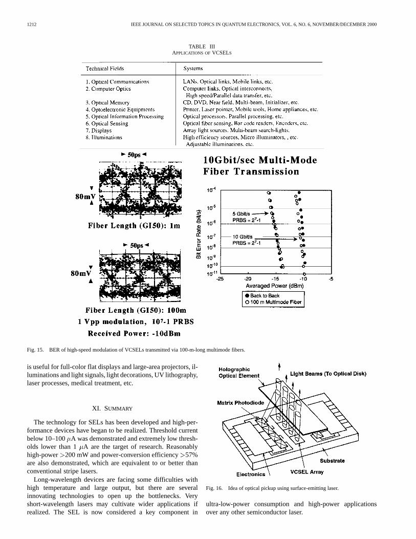
In these low-power consumption devices, high-speed modu-lation is possible in low driving currents around 1 mA as well.This is substantially important in low-power interconnect ap-plications enabling 10 Gb/s transmission or 1 Gb/s zero-biasoperation [48]. Transmission experiments over 10 Gb/s andzero-bias transmission have been reported. We measured aneye diagram for 10 Gb/s transmission experiment through a100-m multimode fiber [49].
Finally, VCSELs in this wavelength may find the market in 10Gb LANs together with high-speed detectors and silica fibers.In any way, GaInAs VCSELs show the best performance, andthe research to challenge the extreme characteristics will be con-tinued.
B. 980-nm GaInAs–GaAs VCSEL on GaAs(311) Substrate
Most of VCSELs grown on GaAs (100) substrates showunstable polarization states due to isotropic material gain andsymmetric cavity structures. VCSELs grown by MBE on GaAs(311) A substrates, however, show a very stable polarizationstate [50]. Also, trials of growth on (GaAs) B substrates byusing MOCVD has been performed [51], [52]. Single trans-verse mode and polarization mode controlled VCSELs havenot been realized at the same time.
In this section, we introduce a single transverse mode andpolarization controlled VCSEL grown on a GaAs (311) B sub-strate. Both higher order transverse modes and a nonlasing or-thogonal polarization modes are well suppressed with a suppres-sion ratio of over 25 dB [53].
The schematic structure of a fabricated top-emitting VCSELgrown on GaAs (311) B is shown in Fig. 10(a), which hasbeen grown by low pressure MOCVD [54]. The bottomn-type DBR consists of 36 pairs of Al Ga As–GaAsdoped with Se. The top p-type DBR consists of 21 pairs ofZn-doped Al Ga As–GaAs and a 70-Å-thick AlAs carbonhigh-doping layer inserted at the upper AlGaAs interface by thecarbon auto-doping technique proposed by us [41]. The activelayer consists of three 8-nm-thick InGa As quantum wellsand 10-nm GaAs barriers surrounded by AlGa As to forma cavity. An 80-nm-thick AlAs was introduced on the uppercavity spacer layer to form an oxide confinement. We oxidizedthe AlAs layer of etched m m mesa at 480C for 5min in an N –H O atmosphere by bubbling in 80C water andformed an oxide aperture of m m.
(a)
(b)
Fig. 10. InGaAs–GaAs VCSEL grown on (311) B substrate. (a) Devicestructure and (b)I–L characteristic exhibiting single mode and singlepolarization.
Fig. 11. Spectra of an oxide-confined InGaAs–GaAs VCSEL formed on (311)B substrate for dc and 5-Gb/s modulation conditions.
Fig. 10(b) shows a typical– and – characteristic underroom-temperature CW operation. The threshold current is 260mA, which is comparable to the lowest value reported fornon(100)-substrate VCSELs. The threshold voltage is 1.5 Vand the maximum output power is 0.7 mW at 4 mA.
In the entire tested driving range , a large side-mode suppression ratio (SMSR) of over 35 dB and an orthog-onal polarization suppression ratio (OPSR) of over 25 dB wereachieved at the same time. The single polarization operation wasmaintained at 5-GHz modulation condition [55], [56], as shownin Fig. 11.
The selective oxidation of AlAs is becoming a standard cur-rent and optical confinement scheme for milliampere thresholddevices. The technology for mode-stable lasers using (311) Bsubstrate is demonstrated for polarization control [56]. We have

IGA: SURFACE-EMITTING LASER—ITS BIRTH AND GENERATION OF NEW OPTOELECTRONICS FIELD 1209
obtained completely single-mode VCSEL by employing mostof the available advanced techniques.
VI. SURFACE-EMITTING LASERS INNEAR INFRARED-RED
BAND
A. 850-nm GaAlAs–GaAs VCSEL
A GaAlAs–GaAs laser can employ almost the same circularburied hetero (CBH) structure as the GaInAsP–InP laser. Inorder to decrease the threshold, the active region is also con-stricted by the selective meltback method. In 1986, a thresholdof 6 mA was demonstrated for the active region diameter munder pulsed operation at 20.5C [4]. The threshold currentdensity is about A m . It is noted that a micro-cavity of 7 m long and 6 m in diameter was realized.
The MOCVD grown CBH VCSEL was demonstratedby a two-step MOCVD growth and fully monolithic tech-nology [57]. The first room-temperature CW operation wasachieved in [5]. The lowest CW threshold current was 20mA A m . The differential quantum effi-ciency is typically 10%. The maximum CW output poweris about 2 mW. The saturation of the output power is dueto a temperature increase of the device. Stable single-modeoperation is observed with neither subtransverse modes norother longitudinal modes. The spectral linewidth above thethreshold is less than 1 Å, which is limited by the resolution ofthe spectrometer. The mode spacing of this device was 170 Å.The side-mode suppression ratio (SMSR) of 35 dB is obtainedat . This is comparable to that of well designedDBR- or DFB-dynamic single-mode lasers.
Submilliampere thresholds and 10-mW outputs have beenachieved. The power conversion efficiency of 57% has beendemonstrated in [58]. Some commercial optical links have al-ready been in markets. The price of low-skew multimode fiberribbons may be a key issue for inexpensive multimode fiber-based data links.
As for the reliability of VCSELs, 10hours of room-temper-ature operation is estimated, based upon the acceleration testat high temperature using proton-defined device [59]. In 1998,some preliminary test results were reported on oxide-defineddevices, exhibiting no substantial negative failures.
B. 780-nm GaAlAs–GaAs VCSEL
The VCSEL in this wavelength was demonstrated in 1987by optical pumping, and the first current injection device wasdeveloped by [9]. If we choose the Al contentto be 0.14 forGa Al As, the wavelength can be as short as 780 nm. Thisis common for compact disc lasers. When the quantum-well isused for active layer, blue shift should be taken into account.
We show the design below [60]. The active layerGa Al As is formed by a super lattice consisting ofGaAs (33.9 Å), and AlAs (5.7 Å), with 14 period. The DBR ismade of AlAs–Al Ga As–Al Ga As–Al Ga Asas 1 period. The n-DBR has 28.5 pair and p-DBR consists of 22pairs. The threshold in 1991 was 4–5 mA and the output was0.7–0.8 mW. Later on, the multiquantum wells (MQW) madeof Al content was introduced, and the thresholdof 200 A and the output of 1.1 mW were demonstrated [60].
C. AlGaInP Red VCSEL
Generally, the light-emitting device in short wavelength re-gions may have more severe operation problems than longerwavelength regions since the photon energy is large and p-typedoping is technically harder to perform. If aluminum is includedin the system, the degradation due to Al-oxidation is appre-ciable. The AlGaInP–GaAs system, emitting red color rangingfrom 630–670 nm, is considered a laser for the first generationdigital video disc system. GaInAlP–GaAs VCSELs are devel-oped; room-temperature operation exhibiting submilliamperethreshold, 8 mW output, and 11% conversion efficiency havebeen obtained [59]. The wavelength is 6720 nm with oxide aper-ture of m m. The threshold is 0.38 mA, the output is0.6 mW, and the maximum operation temperature is 85C [12].In 1998, submilliampere thresholds, 11% power conversion ef-ficiency, 8 mW of output power were achieved [61].
VII. SURFACE-EMITTING LASERS INGREEN–BLUE UV BAND
Visible SELs are extremely important for disk, printers, anddisplay applications. In particular, red, green, and blue surfaceemitters may provide much wider technical applications, if re-alized. The ZnSe system is the material to provide CW op-eration of green-blue semiconductor lasers that operate over1000 hours. It is supposed to be good for green lasers, and theMOCVD may be a key for getting reliable devices in mass pro-duction. We have developed a simple technique to get a highp-doping by an ampule diffusion of LiN to ZnSe. Also, a di-electric mirror deposition was investigated, and relatively highreflectivity was obtained to provide an optical pumped verticalcavity. Some trials regarding optical pumped and current-injec-tion surface-emitting lasers have been made [14].
GaN and related materials can cover wide spectral rangesgreen to UV. The reported reliability of GaN-based LEDs andLDs [62], [63] seems to indicate a good material potentiality forSELs as well.
Optical gain is one of the important parameters to estimatethe threshold current density of GaN-based VCSELs [64]. Theestimation of linear gain for GaN–Al Ga N quantum wellis carried out using the density-matrix theory with intrabandbroadening. The transparent carrier density of GaN is higherthan other III–V materials like as GaAs, presumably origi-nating from its heavy electron and hole masses. Generally,the effective masses of electrons and holes depend on thebandgap energy. Thus, it seems that the wide-bandgap semi-conductors require higher transparent carrier densities thannarrow-bandgap materials. The introduction of quantum wellsfor wide-bandgap lasers is very effective. This result indicatesthat the GaN–Al Ga N quantum well is useful for lowthreshold operation of VCSELs [65].
The trial for realizing green to UV VCSELs has just began.Some optical pumping experiments have been reported [14],[15]. It is necessary to establish some process technologiesfor device fabrication, such as etching, surface passivation,substrate preparation, metallization, current confinementformation, and so on [65]. We have made a preliminary studyto search for dry etch of a GaN system by a chlorine-basedreactive ion beam etch, which was found to be possible.

1210 IEEE JOURNAL ON SELECTED TOPICS IN QUANTUM ELECTRONICS, VOL. 6, NO. 6, NOVEMBER/DECEMBER 2000
The GaN system has large potentialities for short wavelengthlasers. AlN–GaN DBR and ZrO–SiODBR are formed for VC-SELs [64], and some selective growth techniques have been at-tempted. A photo-pumped GaInN VCSEL was reported [15].Also, we are trying to grow GaInN–GaN on silica glass forlarge-area light emitters [66].
VIII. I NNOVATING TECHNOLOGIES
A. Targeting Characteristics
By overcoming any technical problems, such as making tinystructures, ohmic resistance of electrodes, and improving heatsinking, we believe that we can obtain a 1-A device. A lot ofeffort toward improving the characteristics of SELs have beenmade, including surface passivation in the regrowth process forBH, microfabrication, and fine epitaxies.
As introduced before, very low thresholds of around 70, 40,and about 10 A were reported by employing the aforemen-tioned oxidation techniques. Therefore, by optimizing the de-vice structures, we can expect a threshold lower than microam-peres in the future [67].
The efficiency of devices is another important issue forvarious applications. By introducing the oxide confinementscheme, power conversion efficiency has been drasticallyimproved due to the effective current confinement and thereduction of optical losses. Also, the reduction of drivingvoltage by innovating the contacting technology helped a lot.As introduced earlier, higher than 57% of power conversionefficiency, sometimes called wall-plug efficiency, has beenrealized. A noticeable difference of the conventional stripe laseris that high efficiency can be obtained at relatively low drivingranges in the case of VCSELs. Therefore, further improvementmay enable us to achieve highly efficient arrayed devices,which have not been attained in any other type of lasers.
The high-speed modulation capability is very essential forcommunication applications. In VCSELs, 10-Gb/s or highermodulation experiments have been reported. For VCSELsystems, it is a great advantage that over 10-Gb/s modulationis possible at around 1-mA driving levels. This characteristicis preferable for low-power consumption optical interconnectapplications [68].
The final screening for applicability of any component andsystem is reliability of devices. A high-temperature accelera-tion life test of proton-implanted VCSELs showed an expectedroom-temperature lifetime of over 10hours [59]. There is noreason why we can not have very long-life devices by VCSELs,since the active region is completely embedded in wide-gapsemiconductor materials and the mirror is already passivated.
The lasing performance of VCSELs will be improved by op-timizing and solving the following issues: 1) improvement ofcrystal quality; 2) quantum structures (strain, wire/dot, modula-tion doping); 3) polarization control; 4) wavelength control; and5) high-power and low-operation voltage.
Microetching technology is inevitable for making repro-ducible arrayed VCSELs. We have prepared ICP (inductivelycoupled plasma) etching for well-controlled and low-damageetch of GaAs and InP systems [69].
Fig. 12. SEM picture of InP microstructure by ICP etching.
An example of scanning electron microscope (SEM) pictureof an etched InP system for microcavity structure is shown inFig. 12. In order to further achieve substantial innovations inSEL performances, the following technical issues remain un-solved or nonoptimized:
1) AlAs oxidation and its application to current confine-ment and optical beam focusing [70], [71];
2) Modulation doping, p-type, and n-type modulationdoping to quantum wells/barriers;
3) Quantum wires and dots for active engines [72], [73];4) Strained quantum wells and strain compensation;5) Angled substrates, such as (311A), (311B), (411);6) New material combinations such as GaInNAs–GaAs for
long wavelength emission;7) Wafer-fusion technique to achieve optimum combina-
tion of active region and mirrors;8) Transparent mirrors to increase quantum efficiency and
output power;9) Multiquantum barriers to prevent carrier leakage to
p-cladding layer;10) Tunnel junction.Among them, the AlAs oxidation technology seems to be
the most important technology to confine the current to reducethe threshold. Moreover, the oxidized layer works to give someamount of phase shift to focus the beam providing index guidingcavity.
A tunnel junction was introduced in SELs [74]. Recently, thereverse tunnel junction began to be utilized for effective carrierinjection [22] and a noble self-aligned current aperture was pro-posed, as shown in Fig. 13 [22].
B. Polarization Steering
A wide variety of functions, such as polarization control, am-plification, and detection, can be integrated along with SELsby stacking. The polarization control will become very impor-tant for VCSELs [75]. One method incorporates a grating ter-minator to a DBR. The other method includes the utilization of

IGA: SURFACE-EMITTING LASER—ITS BIRTH AND GENERATION OF NEW OPTOELECTRONICS FIELD 1211
Fig. 13. Scheme of parallel fiber-optic module based on surface-emitting laserarray.
Fig. 14. MOB concept to ease the assembling of components without precisealignment.
quantum wires [72] and off-angled substrate, where we can dif-ferentiate the optical gain between one lateral direction and theperpendicular direction [50]. As already introduced, reasonablylow threshold and well controlled polarization behaviors havebeen demonstrated by (311)A and (311)B substrates. The de-vice formation on (311)B GaAs substrates employing MOCVDmethods has been attempted by solving the difficulties of crystalgrowth and p-type doping. We have achieved 260A of CWthreshold, single transverse, and single polarization operation.OPSR of about 30 dB was obtained. In Fig. 11 we show thespectra of a (311) B-based InGaAs–GaAs VCSEL under dc anda 5-Gb/s modulation condition [56]. At a high-speed modula-tion condition, some deterioration of OPSR was observed. Thephysical understanding is not clear at this moment and is opento question. In any way, the use of angled substrates, which pro-vide us with differential gain in two orthogonal polarizations,will be very effective for controlling the polarization indepen-dent of structures and the size of devices.
IX. VCSEL-BASED INTEGRATION TECHNOLOGY
A wide variety of functions, such as frequency tuning, am-plification, and filtering, can be integrated along with SELs bystacking. Another possible way of moduling is to use the micro-optical bench concept [76] to ease the assembling of compo-nents without precise alignment, as shown in Fig. 14. More-over, a 2-D parallel optical-logic system can deal with a largeamount of image information with high speed. To this demand,an SEL will be a key device. Optical neural chips have beeninvestigated for the purpose of making optical neurocomputers
and vertical to surface transmission electro-photonic (VSTEP)integrated device [77].
High power capabilities from VCSELs are very interestingbecause they feature largely extending 2-D arrays. For the pur-pose of realizing coherent arrays, a coherent coupling of thesearrayed lasers has been tried by using a Talbot cavity and con-sidering phase compensation. It is pointed out that 2-D arraysare more suitable to make a coherent array than a linear config-uration since we can take the advantage of 2-D symmetry. Theresearch activity is now forwarded to monolithic integration ofVCSELs, taking the advantage of small-cavity dimensions. Adensely packed array has also been demonstrated for the pur-pose of making high-power lasers and coherent arrays.
Also, there are now attempts to integrate surface-operatingphotonic elements using quantum wells, such as an opticalswitch, frequency tuner, optical filter, and super-lattice func-tional devices. Monolithic lenses can be formed on VCSELsby an etching process to narrow the beam divergence [78].
X. VCSEL APPLICATIONS
Lastly, we consider some possible applications, includingoptical interconnects, parallel fiber-optic subsystems, etc. Wesummarized possible application areas of VCSELs in Table III.
We performed an experiment of10-Gb/s modulation of VC-SELs and transmission via 100-m multimode fibers. The BERis shown in Fig. 15 [79]. Long-wavelength VCSELs should beuseful for silica-based fiber links that provide ultimate transmis-sion capability by taking advantage of single-wavelength op-eration and massively parallel integration. The development of1200–1550-nm VCSELs may be one of the most important is-sues in SEL research [79].
The red-color VCSEL emitting 650 nm can match thelow-loss band of plastic fibers. Short-distance data links areconsidered by using 1-mm diameter plastic fibers with adeveloped graded index. This system provides us with veryeasy optical coupling, and VCSELs can very nicely match thisapplication.
By taking advantage of wide-band and small-volume trans-mission capability, the optical interconnect is considered tobe inevitable in computer technology. A parallel interconnectscheme is wanted and new concepts are being researched. Ver-tical optical interconnect of LSI chips and circuit boards maybe another interesting issue. New architecture for a 64-channelinterconnect has been proposed and a modeling experimentwas performed using GaInAs VCSEL arrays [80].
Several schemes for optical computing have been consid-ered, but one of the bottlenecks may be a lack of suitable op-tical devices, in particular, 2-D VCSELs and surface-operatingswitches. Fortunately, very low threshold VCSELs have beendeveloped, and stack integration together with 2-D photonic de-vices are now considered.
Green to UV VCSELs will be useful in the optoelectronicsfield as in ultra-high density optical memories. We proposed amodel of optical pickup [81] using VCSEL in Fig. 16. This kindof simple pickup is now commercialized. A near-field opticsscheme is considered to realize high-density optical memories[82]. In Fig. 17, a possible device was demonstrated [83], which
1212 IEEE JOURNAL ON SELECTED TOPICS IN QUANTUM ELECTRONICS, VOL. 6, NO. 6, NOVEMBER/DECEMBER 2000
TABLE IIIAPPLICATIONS OFVCSELS
Fig. 15. BER of high-speed modulation of VCSELs transmitted via 100-m-long multimode fibers.
is useful for full-color flat displays and large-area projectors, il-luminations and light signals, light decorations, UV lithography,laser processes, medical treatment, etc.
XI. SUMMARY
The technology for SELs has been developed and high-per-formance devices have began to be realized. Threshold currentbelow 10–100 A was demonstrated and extremely low thresh-olds lower than 1 A are the target of research. Reasonablyhigh-power 200 mW and power-conversion efficiency57%are also demonstrated, which are equivalent to or better thanconventional stripe lasers.
Long-wavelength devices are facing some difficulties withhigh temperature and large output, but there are severalinnovating technologies to open up the bottlenecks. Veryshort-wavelength lasers may cultivate wider applications ifrealized. The SEL is now considered a key component in
Fig. 16. Idea of optical pickup using surface-emitting laser.
ultra-low-power consumption and high-power applicationsover any other semiconductor laser.

IGA: SURFACE-EMITTING LASER—ITS BIRTH AND GENERATION OF NEW OPTOELECTRONICS FIELD 1213
Fig. 17. VCSEL for the generation of optical near field using nano-aperture.
Vertical optical interconnects of LSI chips and circuit boardsand multiple fiber systems may be the most interesting field re-lated to VCSELs. From this point of view, the device shouldbe as small as possible. The future process technology for it, in-cluding epitaxy and etching, will drastically change the situationof VCSELs. Some optical technologies are already introducedin various subsystems and, in addition, the arrayed microoptictechnology would be very helpful for advanced systems.
The most promising application will be gigabit LANs. GaAsVCSELs emitting 850 nm of standardized wavelength aremass produced for 1–Gb/s LAN and simple optical links.For high-end systems, 1300–1550-nm devices are requested.By using VCSEL and micromachining technology, we demon-strated a temperature-insensitive surface normal Fabry–Perotfilter for add–drop filtering in WDM. To establish an appro-priate module technology utilizing VCSELs, an MOB has beeninvestigated together with planar microlens array. Related toplanar microlens array application and ultra-parallel informa-tion processing, an image recognition system is investigatedusing synthetic discriminant function (SDF) filtering.
In summary, the ultra-parallel optoelectronics based upon ar-rayed devices, including VCSELs, will open up a new era forthe 2000 millennium.
ACKNOWLEDGMENT
The author would like to thank Prof. F. Koyama, T.Miyamoto, and other laboratory members for their collabora-tion and assistance in preparing the original drawings.
REFERENCES
[1] K. Iga, F. Koyama, and S. Kinoshita, “Surface emitting semiconductorlaser,”IEEE J. Quant. Electron., vol. 24, pp. 1845–1855, Sept. 1988.
[2] K. Iga, “Surface emitting laser,”Trans. IEICE, C-I, vol. JBl-C-1, no. 9,pp. 483–493, Sept. 1998.
[3] H. Soda, K. Iga, C. Kitahara, and Y. Suematsu, “GaInAsP/InP surfaceemitting injection lasers,”Jpn. J. Appl. Phys., vol. 18, pp. 2329–2330,Dec. 1979.
[4] K. Iga, S. Kinoshita, and F. Koyama, “Microcavity GaAlAs/GaAs sur-face-emitting laser withI = 6mA,” Electron. Lett., vol. 23, no. 3, pp.134–136, Jan. 1987.
[5] F. Koyama, S. Kinoshita, and K. Iga, “Room-temperature continuouswave lasing characteristics of GaAs vertical cavity surface-emittinglaser,”Appl. Phys. Lett., vol. 55, no. 3, pp. 221–222, July 1989.
[6] J. L. Jewell, S. L. McCall, A. Scherer, H. H. Houh, N. A. Whitaker, A. C.Gossard, and J. H. English, “Transverse modes, waveguide dispersionand 30-ps recovery in submicron GaAs/AlAs microresonators,”Appl.Phys. Lett., vol. 55, pp. 22–24, July 1989.
[7] R. Geels and L. A. Coldren, “Narrow-linewidth, low threshold vertical-cavity surface-emitting lasers,” in12th IEEE Int. Semiconductor LaserConf., vol. B-1, 1990, pp. 16–17.
[8] T. Wipiejewski, K. Panzlaf, E. Zeeb, and K. J. Ebeling, “Submilliampvertical cavity laser diode structure with 2.2-nm continuous tuning,” in18th European Conf. Opt. Comm. ’92, Sept. 1992, PDII-4.
[9] Y. H. Lee, B. Tell, K. F. Brown-Goebeler, R. E. Leibenguth, and V.D. Mattera, “Deep-red continuous wave top-surface-emitting vertical-cavity AlGaAs superlattice lasers,”IEEE Photon. Technol. Lett., vol. 3,no. 2, pp. 108–109, Feb. 1991.
[10] T. Miyamoto, T. Uchida, N. Yokouchi, Y. Inaba, F. Koyama, and K. Iga,“A study on gain-resonance matching of CBE grownl = 1:5 �m sur-face emitting lasers,”IEEE/LEOS Annu., no. DLTA13.2, p. 542, Nov.1992.
[11] T. Baba, Y. Yogo, K. Suzuki, F. Koyama, and K. Iga, “Near room tem-perature continuous wave lasing characteristics of GaInAsP/InP surfaceemitting laser,”Electron. Lett., vol. 29, no. 10, pp. 913–914, May 1993.
[12] D. I. Babic, K. Streubel, R. P. Mirin, J. Pirek, N. M. Margalit, J. E.Bowers, E. L. Hu, D. E. Mars, L. Yang, and K. Carey, “Room temper-ature performance of double-fused 1.54�m vertical-cavity lasers,” inIPRM 96, Apr. 1996, no. ThA1-2.
[13] K. D. Choquette, R. P. Schneider, M. H. Crawford, K. M. Geib, and J. J.Figiel, “Continuous wave operation of 640–660 nm selectively oxidisedAlGaInP vertical cavity lasers,”Electron. Lett., vol. 31, pp. 1145–1146,July 1995.
[14] K. Iga, “Possibility of Green/Blue/UV surface emitting lasers,” inInt. Symp. Blue Laser Light Emitting Diodes, Mar. 1996, Th-11, pp.263–266.
[15] T. Someya, K. Tachibana, Y. Arakawa, J. Lee, and T. Kamiya, “Lasingoscillation in InGaN vertical cavity surface emitting lasers,” in16th Int.Semiconductor Laser Conf., 1998, PD-1, pp. 1–2.
[16] S. Uchiyama, N. Yokouchi, and T. Ninomiya, “Room-temperature CWoperation of 1.3-�m GaInAsP SL-MQW surface emitting laser,” in43thSpring Meeting Jpn. Soc. Appl. Phys., 1996, 26p-C-7.
[17] N. M. Margalit, D. I. Babic, K. Streubel, R. P. Mirin, R. L. Naone, J.E. Bowers, and E. L. Hu, “Submilliamp long wavelength vertical cavitylasers,”Electron. Lett., vol. 32, p. 1675, Aug. 1996.
[18] K. A. Black, N. M. Margalit, E. R. Hegblom, P. Abraham, Y.-J. Chiu,J. Piprek, J. E. Bowers, and E. L. Hu, “Double-fused 1.5�m verticalcavity lasers operating continuous wave up to 71C,” in 16th Int. Semi-conductor Laser Conf., 1998, ThA8, pp. 247–248.
[19] V. Jayaraman, J. C. Geske, M. H. MacDougal, F. H. Peters, T. D. Lowes,and T. T. Char, “Uniform threshold current, continuous-wave, singlemode 1300 nm vertical cavity lasers from 0 to 70C,” Electron. Lett.,vol. 34, no. 14, pp. 1405–1407, July 1998.
[20] M. Yamada, T. Anan, K. Kurihara, K. Nishi, K. Tokutome, A. Kamei,and S. Sugou, “Room temperature low threshold CW operation of 1.23�m GaAsSb VCSELs of GaAs substrates,”Electron. Lett., vol. 36, no.7, pp. 637–638, Mar. 2000.
[21] E. Hall, G. Almuneau, J. K. Kim, O. Sjölund, H. Kroemer, and L. A. Col-dren, “Electrically-pumped, single-epitaxial VCSELs at 1.55�m withSb-based mirrors,”Electron. Lett., vol. 35, no. 16, pp. 1337–1338, Aug.1999.
[22] S. Sekiguchi, T. Miyamoto, T. Kimura, F. Koyama, and K. Iga, “Self-arraigned current confinement structure using AlAs/InP tunnel junctionin GaInAsP/InP semiconductor lasers,”Appl. Phys. Lett., vol. 75, no. 11,pp. 1512–1514, Sep. 1999.
[23] C. Kazmierski, J. P. Debray, R. Madani, N. Bouadma, J. Etrillard, I.Sagnes, F. Alexandre, and M. Quillec, “First all-monolithic VCSELs onInP :+55 C pulse lasing at 1.56�m with GaInAlAs/InP system,” in16th Int. Semiconductor Laser Conf., 1998, PD-3, pp. 5–6.
[24] M. Kondow, K. Nakahara, T. Kitatani, Y. Yazawa, and K. Uomi,“GaInNAs laser diode pulsed operation at 77 K,” inOECC’96,18D-3-2.
[25] K. Nakahara, M. Kondow, T. Kitatani, M. C. Larson, and K. Uomi,“1.3-�m continuous-wave lasing operation in GaInNAs quantum-welllasers,”IEEE Photon. Technol. Lett., vol. 10, pp. 487–488, Apr. 1998.
[26] K. Iga, “Vertical cavity surface emitting lasers based on InP and relatedcompounds—Bottleneck and corkscrew,” inConf. Indium PhosphideRelated Materials, Schwabisch Gmund, Germany, Apr. 1996.
[27] T. Miyamoto, K. Takeuchi, F. Koyama, and K. Iga, “NovelGaInNAs/GaAs quantum well structure for long wavelength semicon-ductor lasers,”IEEE Photon. Technol. Lett., vol. 9, pp. 1448–1450,Nov. 1997.
[28] M. C. Larson, M. Kondow, T. Kitatani, K. Nakahara, K. Tamura,H. Inoue, and K. Uomi, “Room-temperature pulsed operationof GaInNAs/GaAs long-wavelength vertical cavity lasers,” inIEEE/LEOS’97, Nov. 1997, no. PD1.3.
[29] T. Kageyama, T. Miyamoto, S. Makino, N. Nishiyama, F. Koyama, andK. Iga, “High-temperature operation up to 170C of GaInNAs–GaAsquantum-well lasers grown by chemical beam epitaxy,”IEEE Photon.Technol. Lett., vol. 12, pp. 10–12, Jan. 2000.

1214 IEEE JOURNAL ON SELECTED TOPICS IN QUANTUM ELECTRONICS, VOL. 6, NO. 6, NOVEMBER/DECEMBER 2000
[30] H. Ishikawa, K. Otsubo, and H. Imai, “Experimental and theoreticalanalysis of the temperature performance of highT lasers on InGaAsternary substrate,” in16th IEEE Int. Semiconductor laser Conf., Oct.1998, TuE51, pp. 195–196.
[31] D. Schlenker, T. Miyamoto, Z. Chen, F. Koyama, and K. Iga, “1.17�m highly strained GaInAs–GaAs quantum-well laser,”IEEE Photon.Technol. Lett., vol. 11, pp. 946–948, Aug. 1999.
[32] Z. Chen, D. Schlenker, T. Miyamoto, T. Kondo, M. Kawaguchi, F.Koyama, and K. Iga, “High-temperature characteristics of near 1.2�m InGaAs/AlGaAs lasers,”Jpn. J. Appl. Phys., vol. 38, no. 10B, pp.L1178–1179, Oct. 1999.
[33] F. Koyama, S. Schlenker, T. Miyamoto, Z. Chen, A. Matsutani, T. Sak-aguchi, and K. Iga, “1.2�m highly strained GaInAs/GaAs quantum-welllasers for single-mode fibre datalink,”Electron. Lett., vol. 35, no. 13, pp.1079–1081, June 1999.
[34] T. Sakaguchi, F. Koyama, and K. Iga, “Vertical cavity surface emittinglaser with and AlGaAs/AlAs Bragg reflector,”Electron. Lett., vol. 24,no. 15, pp. 928–929, July 1988.
[35] T. Numai, T. Kawakami, T. Yoshikawa, M. Sugimoto, Y. Sugimoto, H.Yokoyama, K. Kasahara, and K. Asakawa, “Record low threshold cur-rent in microcavity surface-emitting laser,”Jpn. J. Appl. Phys., vol. 32,no. 10B, pp. L1533–L1534, Oct. 1993.
[36] D. L. Huffaker, D. G. Deppe, C. Lei, and L. A. Hodge, “Sealing AlAsagainst oxidative decomposition and its use in device fabrication,” inCLEO’96, Anaheim, no. JTuH5.
[37] Y. Hayashi, T. Mukaihara, N. Hatori, N. Ohnoki, A. Matsutani, F.Koyama, and K. Iga, “Lasing characteristics of low-threshold oxideconfinement InGaAs–GaAlAs vertical-cavity surface-emitting lasers,”IEEE Photon. Technol. Lett., vol. 7, pp. 1234–1236, Nov. 1995.
[38] , “Record low threshold index-guided InGaAs/GaAlAs vertical-cavity surface-emitting laser with a native oxide confinement structure,”Electron. Lett., vol. 31, no. 7, pp. 560–561, Mar. 1995.
[39] D. L. Huffaker, J. Shin, and D. G. Deppe, “Low threshold half-wave ver-tical-cavity lasers,”Electron. Lett., vol. 30, pp. 1946–1947, Nov. 1994.
[40] G. M. Yang, M. MacDougal, and P. D. Dupkus, “Ultralow threshold cur-rent vertical cavity surface emitting lasers obtained with selective oxi-dation,”Electron. Lett., vol. 31, pp. 886–888, May 1995.
[41] N. Hatori, A. Mizutani, N. Nishiyama, F. Motomura, F. Koyama, andK. Iga, “P-type delta doped InGaAs/GaAs quantum well vertical-cavitysurface-emitting lasers,”IEICE C-I, vol. J81-C-I, no. 7, pp. 410–416,1998.
[42] F. H. Peters, M. G. Peters, D. B. Young, J. W. Scott, B. J. Tibeault, S. W.Corzine, and L. A. Coldren, “High power vertical cavity surface emittinglasers,” in13th IEEE Semiconductor Laser Conf., 1992, PD-1, pp. 1–2.
[43] K. L. Lear, R. P. Schneider Jr., K. D. Choquette, S. P. Kilcoyne, and K. M.Geib, “Selectively oxidised vertical cavity surface emitting lasers with50% power conversion efficiency,”Electron. Lett., vol. 31, pp. 208–209,Feb. 1995.
[44] K. D. Choquette, A. A. Allerman, H. Q. Hou, G. R. Hadley, K. M. Geib,and B. E. Hammons, “Improved efficiency of small area selectively ox-idized VCSELs,” in16th Int. Semiconductor Laser Conf., Oct. 1998,ThA3, pp. 237–238.
[45] L. A. Coldren, E. R. Hegblom, and N. M. Margalit, “Vertical cavitylasers with record efficiency at small sizes using tapered apertures,” in16th Int. Semiconductor Laser Conf., Oct. 1998, PD-2, pp. 3–4.
[46] B. Weigl, G. Reiner, M. Grabherr, and K. J. Ebeling, “High-power se-lectively oxidized vertical-cavity surface-emitting lasers,” inCLEO’96,Anaheim, June 1996, JTuH2.
[47] D. Francis, H.-I. Chen, W. Yuen, G. Li, and C. Chang-Hasnain, “Mono-lithic 2D-VCSEL array with 0.2 W CW output power,” in16th Int. Semi-conductor Laser Conf., Oct. 1998, TuE3, pp. 99–100.
[48] B. J. Thibeault, K. Bertilsson, E. R. Hegblom, P. D. Floyd, and L. A. Col-dren, “High-speed modulation characteristics of oxide-apertured ver-tical-cavity lasers,” in15th IEEE Int. Semicon. Laser Conf., 1996, M3.2,pp. 17–18.
[49] N. Hatori, A. Mizutani, N. Nishiyama, A. Matsutani, T. Sakaguchi,F. Motomura, F. Koyama, and K. Iga, “An over 10 Gb/s transmissionexperiment using p-type d-doped InGaAs/GaAs quantum-well verticalcavity surface-emitting laser,”IEEE Photon. Technol. Lett., vol. 10, pp.194–196, Feb. 1998.
[50] M. Takahashi, N. Egami, T. Mukaihara, F. Koyama, and K. Iga, “Lasingcharacteristics of GaAs (311)A substrate based InGaAs/GaAs verticalcavity surface emitting lasers,”IEEE J. Select. Topics Quantum Elec-tron., vol. 3, no. 2, pp. 372–378, Apr. 1997.
[51] K. Tateno, Y. Ohiso, C. Amano, A. Wakatsuki, and T. Kurokawa,“Growth of vertical-cavity surface-emitting laser structures on GaAs(311)B substrates by metalorganic chemical vapor deposition,”Appl.Phys. Lett., vol. 70, no. 25, pp. 3395–3396, June 1997.
[52] A. Mizutani, N. Hatori, N. Ohnoki, N. Nishiyama, N. Ohtake, F.Koyama, and K. Iga, “P-type doped AlAs growth on GaAs (311)Bsubstrate using carbon auto-doping for low resistance GaAs/AlAsdistributed Bragg reflectors,”Jpn. J. Appl. Phys., vol. 36, no. 11, pp.6728–6729, Nov. 1997.
[53] A. Mizutani, N. Hatori, N. Nishiyama, F. Koyama, and K. Iga, “A lowthreshold polarization-controlled vertical cavity laser grown on GaAs(311) substrate,”IEEE Photon. Technol. Lett., vol. 10, pp. 633–635, May1998.
[54] N. Nishiyama, A. Mizutani, N. Hatori, F. Koyama, and K. Iga, “Singlemode and stable polarization InGaAs/GaAs surface emitting laser grownon GaAs (311)B substrate,” in16th Int. Semiconductor Laser Conf.,1998, ThA1, pp. 233–234.
[55] , “Single transversemode and stable polarization operation underhigh-speed modulation of InGaAs/GaAs vertical cavity surface emittinglaser grown on GaAs (311)B substrate,”IEEE Photon. Technol. Lett.,vol. 10, pp. 1676–1678, Dec. 1998.
[56] N. Nishiyama, A. Mizutani, N. Hatori, M. Arai, F. Koyama, and K.Iga, “Lasing characteristics of InGaAs/GaAs polarization controlled ver-tical-cavity surface emitting laser grown on GaAs (311) B substrate,”Select. Topics Quantum Electron., vol. 5, pp. 530–536, Feb. 1999.
[57] F. Koyama, K. Tomomatsu, and K. Iga, “GaAs surface emitting laserswith circular buried heterostructure grown by metalorganic chemicalvapor deposition and two-dimensional laser array,”Appl. Phys. Lett.,vol. 52, no. 7, pp. 528–529, Feb. 1988.
[58] R. Jager, M. Grabherr, C. Jung, R. Michalzik, G. Reiner, B. Weigl, and K.J. Ebeling, “57% wallplug efficiency oxide-confined 850 nm wavelengthGaAs VCSELs,”Electron. Lett., vol. 33, no. 4, pp. 330–331, Feb. 1997.
[59] J. K. Guenter, R. A. Hawthorne, D. N. Granville, M. K. Hibbs-Brenner,and R. A. Morgan, “Reliability of proton-implanted VCSELs for datacommunications,”Proc. SPIE, vol. 2683, p. 1, 1996.
[60] H.-E. Shin, Y.-G. Ju, H.-H. Shin, J.-H. Ser, T. Kim, E.-K. Lee, I. Kim,and Y. -H. Lee, “780 nm oxidised vertical-cavity surface-emitting laserswith Al Ga As quantum wells,”Electron. Lett., vol. 32, no. 14,pp. 1287–1288, July 1996.
[61] M. H. Crawford, K. D. Choquette, R. J. Hickman, and K. M. Geib, “Per-formance of selectively oxidized AlGaInP-based visible VCSELs,”OSATrends Optics Photon. Series, vol. 15, pp. 104–105, 1998.
[62] S. Nakamura, M. Senoh, S. Nagahama, N. Iwasa, T. Yamada, T. Mat-sushita, H. Kiyoku, and Y. Sugimoto, “InGaN-based multi-quantum-well-structure laser diodes,”Jpn. J. Appl. Phys., pt. 2, vol. 35, no. 1B,pp. L74–L76, Jan. 1996.
[63] S. Nakamura, M. Senoh, S. Nagahama, N. Iwasa, T. Yamada, T. Mat-sushita, H. Kiyoku, Y. Sugimoto, T. Kozaki, H. Umemoto, M. Sano,and K. Chocho, “High-power, long-lifetime InGaN/GaN/AlGAN-basedlaser diodes grown on pure GaN substrates,”Jpn. J. Appl. Phys., vol. 37,pp. L309–L312, Mar. 1998.
[64] T. Sakaguchi, T. Shirasawa, N. Mochida, A. Inoue, M. Iwata, T. Honda,F. Koyama, and K. Iga, “Highly reflective AlN/GaN and ZrO/SiOmultilayer distributed Bragg reflectors for InGaN/GaN surface emittinglasers,” inLEOS 1998 11th Annual Meeting Conf. Proc., TuC4, Dec.1998.
[65] T. Shirasawa, N. Mochida, A. Inoue, T. Honda, T. Sakaguchi, F. Koyama,and K. Iga, “Interface control of GaN/AlGaN quantum well structuresin MOVPE growth,”J. Cryst. Growth, pp. 124–127, 1998.
[66] Y. Moriguchi, T. Miyamoto, T. Sakaguchi, M. Iwata, Y. Uchida, F.Koyama, and K. Iga, “GaN polycrystal growth on silica substrate bymetalorganic vapor phase epitaxy (MOVPE),” in3rd Int. Symp. BlueLaser Light Emitting Diodes, Berlin, Mar. 2000, WeP-19, p. 83.
[67] K. Iga and F. Koyama, “Surface emitting lasers,” inAcademic Monthly,Gakujyutsu-Geppo; JSPS ed., Jan. 1996, vol. 49, no. 1, pp. 42–46.
[68] B. E. Lemoff and L. A. Buckman, “Low-cost WDM transceivers for theLAN,” in Dig. LEOS-Summer Topical Meeting, 1999, MA2.1, pp. 3–4.
[69] A. Matsutani, H. Ohtsuki, F. Koyama, and K. Iga, “C60 resist maskof electron beam lithography for chlorine-based reactive ion beametching,”Jpn. J. Appl. Phys., vol. 37, no. 7, pp. 4211–4212, July 1998.
[70] D. G. Deppe, D. L. Huffaker, J. Shin, and Q. Deng, “Very-low-thresholdindex-confined planar microcavity lasers,”IEEE Photon. Technol. Lett.,vol. 7, pp. 965–967, Sept. 1995.
[71] H. Bissessur, F. Koyama, and K. Iga, “Modeling of oxide-confined ver-tical cavity surface emitting lasers,”IEEE J. Quantum Electron., vol. 3,pp. 344–352, Apr. 1997.
[72] N. Hatori, T. Mukaihara, Y. Hayashi, N. Ohnoki, F. Koyama, and K. Iga,“Design and fabrication of InGaAs/GaAs quantum wires for vertical-cavity surface-emitting lasers,”Jpn. J. Appl. Phys., vol. 35, no. 3, pp.1777–1778, Mar. 1996.

IGA: SURFACE-EMITTING LASER—ITS BIRTH AND GENERATION OF NEW OPTOELECTRONICS FIELD 1215
[73] D. G. Deppe, D. L. Huffaker, Q. Deng, T.-H. Oh, and L. A. Graham,“Oxide-confined VCSELs with quantum well quantum dot active re-gion,” in IEEE/LEOS’97, Nov. 1997, no. ThA 1, pp. 287–288.
[74] Y. Kotaki, S. Uchiyama, and K. Iga, “GaInAsP/InP surface emitting laserwith two active layers,” in1984 Int. Conf. Solid-State Devices, no. C-2-3.
[75] T. Mukaihara, N. Ohnoki, Y. Hayashi, N. Hatori, F. Koyama, and K.Iga, “Polarization control of vertical-cavity surface-emitting lasersusing a birefringent metal/dielectric polarizer loaded on top distributedBragg reflector,”IEEE J. Select. Topics Quantum Electron., vol. 1, pp.667–673, June 1995.
[76] Y. Aoki, R. J. Mizuno, Y. Shimada, and K. Iga, “Parallel and bi-direc-tional optical interconnect module using vertical cavity surface emit-ting lasers(VCSELs) and 3-D micro optical bench (MOB),” in1999IEEE/LEOS Summer Topical Meetings, July 1999, WA2.4, pp. 9–10.
[77] T. Numai, M. Sugimoto, I. Ogura, H. Kosaka, and K. Kasahara, “Cur-rent versus light-output characteristics with no definite threshold in pnpnvertical to surface transmission electro-photonic devices with a verticalcavity,” Jpn. J. Appl. Phys., vol. 30, no. 4A, pp. L602–L604, Apr. 1991.
[78] K. Iga, T. Kambayashi, K. Wakao, C. Kitahara, and K. Moriki,“GaInAsP/InP double-structure planar LEDs,”IEEE Trans. Electron.Devices, vol. ED-26, pp. 1227–1230, Aug. 1979.
[79] F. Koyama, D. Schlenker, T. Miyamoto, Z. Chen, A. Matsutani, T. Sak-aguchi, and K. Iga, “Data transmission over single-mode fiber by using1.2-mm uncooled GaInAs–GaAs laser for Gb/s local area network,”IEEE Photon. Technol. Lett., vol. 12, pp. 125–127, Feb. 2000.
[80] H. Kosaka, M. Kajita, Y. Li, and Y. Sugimoto, “A two-dimensional op-tical parallel transmission using a vertical-cavity surface-emitting laserarray module and an image fiber,”IEEE Photon. Technol. Lett., vol. 9,pp. 253–255, Feb. 1997.
[81] K. Iga, “Surface operating electrooptic devices and their applicationto array parallel signal processing,” inECOC’90, vol. 2, Sept. 1990,WeB-2.1, pp. 895–932.
[82] K. Goto, “Tera bytes optical disk with electric tracking control usingmicro-cavity VCSEL array and PD array,” inDig. LEOS-Summer Top-ical Meeting, 1997, MC-4, pp. 21–22.
[83] T. Yamatoya, S. Mori, F. Koyama, and K. Iga, “Design and fabrica-tion of high power and broad-band GaInAsP/InP strained quantum wellsuperluminescent diodes with tapered active region,” inCLEO PacificRim’99, July 1999, FO6v, pp. 1227–1228.
Kenichi Iga (S’67–M’68–SM’80–F’87) was born inHiroshima Prefecture, Japan, in 1940. He receivedthe B.E., M.E., Dr.Eng. degrees from the Tokyo In-stitute of Technology, Tokyo, Japan, in 1963, 1965,and 1968, respectively.
In 1968, he joined the P & I Laboratories,Tokyo Institute of Technology, where he became anAssociate Professor in 1973 and Professor in 1984.Since 1993, he has been a Teiichi Yamazaki ChairProfessor. He is currently the Director of InstituteLibrary and the Director of P & I Microsystem
Research Center. From 1979 to 1980, he was with Bell Laboratories as aVisiting Technical Staff Member. He is the author of many books, includingFundamentals of Microoptics(New York: Academic),Fundamentals of LaserOptics (New York: Plenum),Introduction to Optical Fiber Communication(New York: Wiley), andProcess Technology for Semiconductor Lasers(NewYork: Springer-Verlag). He first proposed and pioneered the research ofsurface-emitting semiconductor lasers, which triggered research activitiesin surface-emitting lasers and has become very important as coherentlight-sources with two-dimensional (2-D) parallelism. His research interestsinclude microoptics, gradient-index microlens arrays, and the realization of2-D arrayed optical devices in combination with surface-emitting lasers.
Prof. Iga is a Member of the Institute of Electronics, Information, and Com-munication Engineers of Japan (IEICE) and a Fellow of the Optical Society ofAmerica. He has served as an Asian Representative for the IEEE Lasers andElectro-Optics Society (IEEE/LEOS) from 1984 to 1990, CLEO Japanese Sub-committee Chair from 1988 to 1990, Board of Governor for IEEE/LEOS from1991 to 1993, and President of the Electronics Society in 1996. He has receivednumerous awards, including the Inada Memorial Prize in 1966, IEICE Distin-guished Book Award forIntroduction to Optical Fiber Communicationsin 1978,the Sakurai Memorial Prize from the Optoelectronic Industry and TechnologyDevelopment Association in 1987, IEE Premium Award in 1988, the WilliamStreifer Award for Scientific Achievement in 1992, the Toray Award in 1995,the IEEE Third Millennium Medal, and the John Tyndall Awardin 1998.