Surface Collective Modes in the Topological Insulators Bi2Se3 and ... · Surface Collective Modes...
5
Surface Collective Modes in the Topological Insulators Bi 2 Se 3 and Bi 0.5 Sb 1.5 Te 3−x Se x A. Kogar, 1 S. Vig, 1 A. Thaler, 1 M. H. Wong, 1 Y. Xiao, 1 D. Reig-i-Plessis, 1 G. Y. Cho, 2 T. Valla, 3 Z. Pan, 3 J. Schneeloch, 3 R. Zhong, 3 G. D. Gu, 3 T. L. Hughes, 1 G. J. MacDougall, 1 T.-C. Chiang, 1 and P. Abbamonte 1,* 1 Department of Physics and Seitz Materials Research Laboratory, University of Illinois, Urbana, Illinois 61801, USA 2 Department of Physics, Korea Advanced Institute of Science and Technology, Daejeon 305-701, Korea 3 Condensed Matter Physics and Materials Science Department, Brookhaven National Laboratory, Upton, New York 11973, USA (Received 22 May 2015; revised manuscript received 29 October 2015; published 15 December 2015) We used low-energy, momentum-resolved inelastic electron scattering to study surface collective modes of the three-dimensional topological insulators Bi 2 Se 3 and Bi 0.5 Sb 1.5 Te 3−x Se x . Our goal was to identify the “spin plasmon” predicted by Raghu and co-workers [Phys. Rev. Lett. 104, 116401 (2010)]. Instead, we found that the primary collective mode is a surface plasmon arising from the bulk, free carriers in these materials. This excitation dominates the spectral weight in the bosonic function of the surface χ } ðq; ωÞ at THz energy scales, and is the most likely origin of a quasiparticle dispersion kink observed in previous photoemission experiments. Our study suggests that the spin plasmon may mix with this other surface mode, calling for a more nuanced understanding of optical experiments in which the spin plasmon is reported to play a role. DOI: 10.1103/PhysRevLett.115.257402 PACS numbers: 78.68.+m, 78.20.Ci, 79.20.Uv The defining characteristics of the three-dimensional topological insulators are a bulk gap and the presence of surface states that cannot be gapped by any time-reversal symmetric type of disorder [1–5]. At its Γ point, the prototypical Bi 2 Se 3 system exhibits a single surface Dirac cone characterized by locking between the quasi- particle spin and momentum [6–11]. Several years ago, Raghu and co-workers predicted that these surface states should give rise to a new type of collective mode, which they termed a “spin plasmon” [12]. This mode is plasmonlike in the sense that it arises from random-phase approximation screening effects but exhibits a spin current because of the spin-textured character of the surface states. This mode is of both fundamental and practical importance for several reasons. First, its existence is a consequence of electron-electron interactions, and hence is an essential many-body effect in materials that are, traditionally, thought of as independent- electron band insulators [1–5]. Second, recent angle- resolved photoemission (ARPES) studies reported the presence of dispersion kinks in the Dirac quasiparticles in both Bi 2 Se 3 and its superconducting cousin Cu x Bi 2 Se 3 , indicating interaction with some bosonic collective mode [13–17], for which the spin plasmon is a prime candidate. The spin plasmon also has potential application bridging the areas of surface plasmonics and spintronics, by providing a coupling between surface collective modes and spin degrees of freedom [18–20]. The primary experimental evidence for this mode comes from pioneering infrared transmission measurements of Bi 2 Se 3 nanoribbons, which were fabricated by e-beam lithography and reactive ion etching [19,21,22]. An excita- tion was observed in the THz regime, whose dispersion exhibited the ffiffiffi q p dependence expected of the spin plasmon [12]. It is crucially important, however, to detect this excitation on a pristine, unpatterned surface, both to cor- roborate the THz experiment and to understand the dynamics of this excitation in a native material. Here, we present measurements of the surface collec- tive modes of Bi 2 Se 3 and Bi 0.5 Sb 1.5 Te 3−x Se x (BSTS) using low-energy, momentum-resolved electron energy-loss spectroscopy (MEELS). MEELS is an inelastic scattering technique that measures the dynamic structure factor of a surface, Sðq; ωÞ [23], which is the Fourier transform of the surface density-density correlation function. Sðq; ωÞ is proportional to the bosonic spectral function, χ } ðq; ωÞ, via the fluctuation-dissipation theorem [23]. χ } ðq; ωÞ directly reveals the charged collective modes of a surface in the meV range, and this makes MEELS an ideal technique to detect the presence of the spin plasmon in an unpatterned surface. To conduct the experiment, single crystals of Bi 2 Se 3 were grown from a melt by techniques described pre- viously [24]. The Se vapor pressures were varied to adjust the concentration of vacancies, which determine the degree of electron doping [24]. The crystals were char- acterized using dc Hall measurements, and labeled 1A–7A in ascending order of bulk carrier density, which ranged from n e ¼ 1.3 × 10 18 cm −3 to n e ¼ 2 × 10 19 cm −3 . Single crystals with nominal composition Bi 0.5 Sb 1.5 Te 3−x Se x were grown from high-purity (99.9999%) elements of Bi, Sb, Te, and Se using the floating-zone method. These PRL 115, 257402 (2015) PHYSICAL REVIEW LETTERS week ending 18 DECEMBER 2015 0031-9007=15=115(25)=257402(5) 257402-1 © 2015 American Physical Society
Transcript of Surface Collective Modes in the Topological Insulators Bi2Se3 and ... · Surface Collective Modes...
Surface Collective Modes in the Topological Insulators Bi2Se3 and Bi0.5Sb1.5Te3−xSex
A. Kogar,1 S. Vig,1 A. Thaler,1 M. H. Wong,1 Y. Xiao,1 D. Reig-i-Plessis,1 G. Y. Cho,2
T. Valla,3 Z. Pan,3 J. Schneeloch,3 R. Zhong,3 G. D. Gu,3 T. L. Hughes,1 G. J. MacDougall,1
T.-C. Chiang,1 and P. Abbamonte1,*1Department of Physics and Seitz Materials Research Laboratory, University of Illinois, Urbana, Illinois 61801, USA
2Department of Physics, Korea Advanced Institute of Science and Technology, Daejeon 305-701, Korea3Condensed Matter Physics and Materials Science Department, Brookhaven National Laboratory,
Upton, New York 11973, USA(Received 22 May 2015; revised manuscript received 29 October 2015; published 15 December 2015)
We used low-energy, momentum-resolved inelastic electron scattering to study surface collective modesof the three-dimensional topological insulators Bi2Se3 and Bi0.5Sb1.5Te3−xSex. Our goal was to identify the“spin plasmon” predicted by Raghu and co-workers [Phys. Rev. Lett. 104, 116401 (2010)]. Instead, wefound that the primary collective mode is a surface plasmon arising from the bulk, free carriers in thesematerials. This excitation dominates the spectral weight in the bosonic function of the surface χ}ðq;ωÞ atTHz energy scales, and is the most likely origin of a quasiparticle dispersion kink observed in previousphotoemission experiments. Our study suggests that the spin plasmon may mix with this other surfacemode, calling for a more nuanced understanding of optical experiments in which the spin plasmon isreported to play a role.
DOI: 10.1103/PhysRevLett.115.257402 PACS numbers: 78.68.+m, 78.20.Ci, 79.20.Uv
The defining characteristics of the three-dimensionaltopological insulators are a bulk gap and the presence ofsurface states that cannot be gapped by any time-reversalsymmetric type of disorder [1–5]. At its Γ point, theprototypical Bi2Se3 system exhibits a single surfaceDirac cone characterized by locking between the quasi-particle spin and momentum [6–11].Several years ago, Raghu and co-workers predicted that
these surface states should give rise to a new type ofcollective mode, which they termed a “spin plasmon”[12]. This mode is plasmonlike in the sense that it arisesfrom random-phase approximation screening effects butexhibits a spin current because of the spin-texturedcharacter of the surface states. This mode is of bothfundamental and practical importance for several reasons.First, its existence is a consequence of electron-electroninteractions, and hence is an essential many-body effect inmaterials that are, traditionally, thought of as independent-electron band insulators [1–5]. Second, recent angle-resolved photoemission (ARPES) studies reported thepresence of dispersion kinks in the Dirac quasiparticlesin both Bi2Se3 and its superconducting cousin CuxBi2Se3,indicating interaction with some bosonic collective mode[13–17], for which the spin plasmon is a prime candidate.The spin plasmon also has potential application bridgingthe areas of surface plasmonics and spintronics, byproviding a coupling between surface collective modesand spin degrees of freedom [18–20].The primary experimental evidence for this mode comes
from pioneering infrared transmission measurements ofBi2Se3 nanoribbons, which were fabricated by e-beam
lithography and reactive ion etching [19,21,22]. An excita-tion was observed in the THz regime, whose dispersionexhibited the
ffiffiffiq
pdependence expected of the spin plasmon
[12]. It is crucially important, however, to detect thisexcitation on a pristine, unpatterned surface, both to cor-roborate the THz experiment and to understand the dynamicsof this excitation in a native material.Here, we present measurements of the surface collec-
tive modes of Bi2Se3 and Bi0.5Sb1.5Te3−xSex (BSTS) usinglow-energy, momentum-resolved electron energy-lossspectroscopy (MEELS). MEELS is an inelastic scatteringtechnique that measures the dynamic structure factor of asurface, Sðq;ωÞ [23], which is the Fourier transform of thesurface density-density correlation function. Sðq;ωÞ isproportional to the bosonic spectral function, χ}ðq;ωÞ, viathe fluctuation-dissipation theorem [23]. χ}ðq;ωÞ directlyreveals the charged collective modes of a surface in themeV range, and this makes MEELS an ideal technique todetect the presence of the spin plasmon in an unpatternedsurface.To conduct the experiment, single crystals of Bi2Se3
were grown from a melt by techniques described pre-viously [24]. The Se vapor pressures were varied to adjustthe concentration of vacancies, which determine thedegree of electron doping [24]. The crystals were char-acterized using dc Hall measurements, and labeled 1A–7Ain ascending order of bulk carrier density, which rangedfrom ne ¼ 1.3 × 1018 cm−3 to ne ¼ 2 × 1019 cm−3. Singlecrystals with nominal composition Bi0.5Sb1.5Te3−xSexwere grown from high-purity (99.9999%) elements ofBi, Sb, Te, and Se using the floating-zone method. These
PRL 115, 257402 (2015) P HY S I CA L R EV I EW LE T T ER Sweek ending
18 DECEMBER 2015
0031-9007=15=115(25)=257402(5) 257402-1 © 2015 American Physical Society
crystals are labeled 1B–7B in ascending order of x, whichwas varied over the range 1.5 ≤ x ≤ 2.2.The crystals were characterized with ARPES to establish
the location of the Fermi energy relative to the bulk bandsand Dirac surface states. The Fermi energy of some Bi2Se3crystals in batches 1A–3A was found to reside in the bulkgap, but all crystals from batches 4A–7Awere found to havethe Fermi energy in the conduction band [Figs. 1(a)–1(c)].We note that, while the bulk carrier density as measured byHall effect was uniform within a growth batch, the Fermienergy measured with ARPES was highly variable, particu-larly for crystals with lower vacancy concentration. Thisvariation was observed previously and attributed to bandbending due to differences in surface termination uponcleaving [24]. The Fermi energy in all BSTS crystals wasfound to reside near the Dirac point, with crystals frombatches 3B–7B being slightly p type and those from batches1B and 2B slightly n type [Figs. 1(d) and 1(f)]. Note that thevalence band in BSTS rises very close to the Dirac point,suggesting bulk carriers may be present even for nearlyneutral materials.For MEELS measurements, crystals were cleaved at
room temperature in ultrahigh vacuum and measuredwithin 30 min, unless stated otherwise [25,26]. Thespectrometer used was of the Ibach variety equipped witha double-pass monochromator and an energy analyzer todisperse the scattered electrons onto the detector [27]. Toachieve momentum resolution, the spectrometer wasequipped with a motorized scattering angle and mated toa custom low-temperature sample goniometer actuated witha piezoelectric motor and differentially pumped rotaryfeedthrough. Using several sets of translations, the various
rotation axes were aligned to intersect the electron beam ata single point. A control system similar to that used in tripleaxis neutron scattering was employed to allow true recip-rocal space scanning. The typical energy resolution was∼10 meV while the momentum resolution was 0.03 Å−1.The incident beam energy was 50 eV for all measurements.MEELS measurements, taken at room temperature for
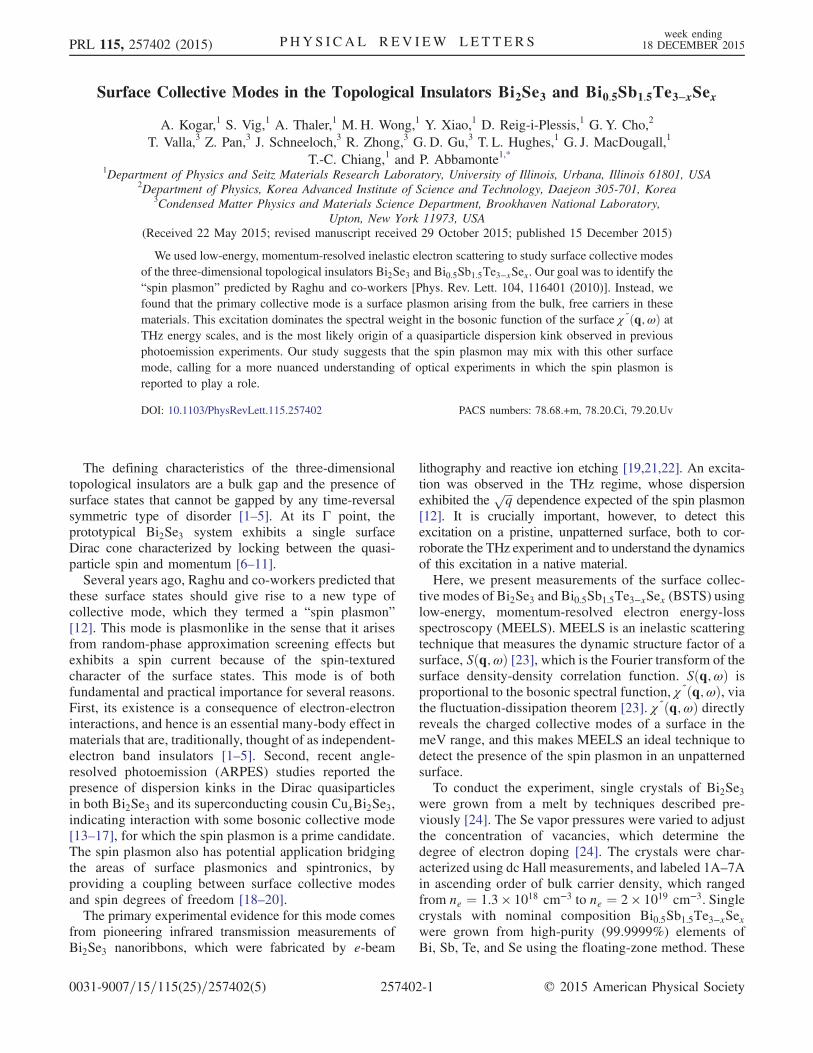
Bi2Se3 and T ¼ 100 K for BSTS, are shown in Fig. 2.The primary feature in both materials is a high-intensityinelastic peak whose energy in the Bi2Se3 system variesfrom 23–90 meV, depending upon the bulk carrier density(the peak centered at zero energy is elastic scattering fromthe crystal surface). In addition, at high doping levels aweak, secondary excitation—with much smaller spectralweight—is observed in Bi2Se3 [Fig. 4(b)]. This mode maybe identified as the out-of-plane A1g phonon previouslyobserved in Raman scattering studies [28,29].While it is tempting to identify the primary excitation as
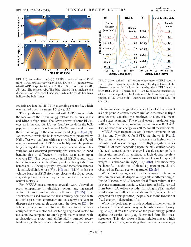
the spin plasmon, its dispersion suggests a different origin.Figure 3 shows MEELS spectra for different values of thein-plane momentum transfer q taken from a Bi2Se3 crystalfrom batch 3A (other crystals, including BSTS, yieldedsimilar results). Rather than exhibiting the
ffiffiffiq
pdependence
expected for a spin plasmon, the peak was found to reside atfixed energy, independent of q.While the peak energy is independent of momentum, it
changes in a systematic way with bulk carrier density.Figure 4(a) shows the square of the peak energy plottedagainst the carrier density ne determined from Hall mea-surements. This plot shows a linear relationship to a highdegree of accuracy, indicating that the excitation energy
FIG. 1 (color online). (a)–(c) ARPES spectra taken at 55 Kfrom Bi2Se3 crystals from batches 6A, 1A, and 3A, respectively.(d)–(f) ARPES spectra taken at 20 K of BSTS from batches 7B,5B, and 2B, respectively. The blue dashed lines indicate thedispersions of the surface Dirac bands while the red dashed linesindicate the bulk bands.
–100 –50 0 50 100Energy Loss (meV)
Inte
nsi
ty(a
rb. u
nit
s)
(a)
Carrier
Density
(×1018 cm- 3)
1.2 ± 0.1
1.3 ± 0.3
3.4 ± 0.4
3.1 ± 0.8
4 ± 1
12 ± 2
20 ± 1
1A
2A
3A
4A
5A
6A
7A
Sample
Batch
Bi2Se3
–40 –20 0 20 40 60 80Energy Loss (meV)
Sample
Batch
Bi0.5Sb1.5Te3- xSex
1B
2B
3B
4B
5B
6B
7B
x=1.5
x=1.6
x=1.66
x=1.76
x=1.9
x=2.1
x=2.2
(b)
FIG. 2 (color online). (a) Room-temperature MEELS spectrafrom Bi2Se3, taken at q ¼ 0, showing the dependence of theplasmon peak on the bulk carrier density. (b) MEELS spectrafrom BSTS at q ¼ 0 taken at T ¼ 100 K, showing insensitivityof the plasmon peak to the location of the Fermi energy withrespect to the Dirac point (spectra are displaced vertically forclarity).
PRL 115, 257402 (2015) P HY S I CA L R EV I EW LE T T ER Sweek ending
18 DECEMBER 2015
257402-2
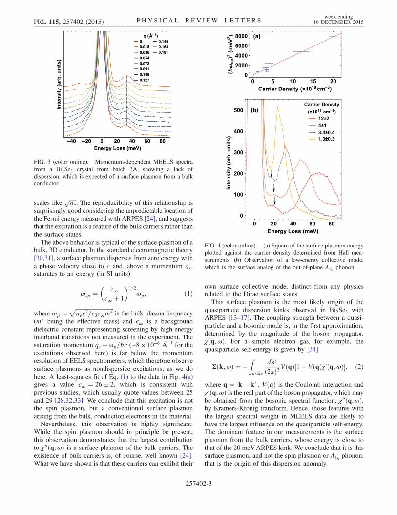
scales likeffiffiffiffiffine
p. The reproducibility of this relationship is
surprisingly good considering the unpredictable location ofthe Fermi energy measured with ARPES [24], and suggeststhat the excitation is a feature of the bulk carriers rather thanthe surface states.The above behavior is typical of the surface plasmon of a
bulk, 3D conductor. In the standard electromagnetic theory[30,31], a surface plasmon disperses from zero energy witha phase velocity close to c and, above a momentum qs,saturates to an energy (in SI units)
ωsp ¼�
ϵ∞ϵ∞ þ 1
�1=2
ωp; ð1Þ
where ωp ¼ffiffiffiffiffiffiffiffiffiffiffiffiffiffiffiffiffiffiffiffiffiffiffiffiffiffiffinee2=ϵ0ϵ∞m�p
is the bulk plasma frequency(m� being the effective mass) and ϵ∞ is a backgrounddielectric constant representing screening by high-energyinterband transitions not measured in the experiment. Thesaturation momentum qs ∼ ωp=ℏc (∼8 × 10⁻⁶ Å−1 for theexcitations observed here) is far below the momentumresolution of EELS spectrometers, which therefore observesurface plasmons as nondispersive excitations, as we dohere. A least-squares fit of Eq. (1) to the data in Fig. 4(a)gives a value ϵ∞ ¼ 26� 2, which is consistent withprevious studies, which usually quote values between 25and 29 [28,32,33]. We conclude that this excitation is notthe spin plasmon, but a conventional surface plasmonarising from the bulk, conduction electrons in the material.Nevertheless, this observation is highly significant.
While the spin plasmon should in principle be present,this observation demonstrates that the largest contributionto χ00ðq;ωÞ is a surface plasmon of the bulk carriers. Theexistence of bulk carriers is, of course, well known [24].What we have shown is that these carriers can exhibit their
own surface collective mode, distinct from any physicsrelated to the Dirac surface states.This surface plasmon is the most likely origin of the
quasiparticle dispersion kinks observed in Bi2Se3 withARPES [13–17]. The coupling strength between a quasi-particle and a bosonic mode is, in the first approximation,determined by the magnitude of the boson propagator,χðq;ωÞ. For a simple electron gas, for example, thequasiparticle self-energy is given by [34]
Σðk;ωÞ ¼ −Zk<kF
dk0
ð2πÞ2 VðqÞ½1þ VðqÞχ0ðq;ωÞ�; ð2Þ
where q ¼ jk − k0j, VðqÞ is the Coulomb interaction andχ0ðq;ωÞ is the real part of the boson propagator, which maybe obtained from the bosonic spectral function, χ00ðq;ωÞ,by Kramers-Kronig transform. Hence, those features withthe largest spectral weight in MEELS data are likely tohave the largest influence on the quasiparticle self-energy.The dominant feature in our measurements is the surfaceplasmon from the bulk carriers, whose energy is close tothat of the 20 meVARPES kink. We conclude that it is thissurface plasmon, and not the spin plasmon or A1g phonon,that is the origin of this dispersion anomaly.
q (Å- 1)00.0180.0360.0540.0730.0910.1090.127
0.1450.1630.181
–40 –20 0 20 40 60 80Energy Loss (meV)
Inte
nsi
ty(a
rb. u
nit
s)
FIG. 3 (color online). Momentum-dependent MEELS spectrafrom a Bi2Se3 crystal from batch 3A, showing a lack ofdispersion, which is expected of a surface plasmon from a bulkconductor.
FIG. 4 (color online). (a) Square of the surface plasmon energyplotted against the carrier density determined from Hall mea-surements. (b) Observation of a low-energy collective mode,which is the surface analog of the out-of-plane A1g phonon.
PRL 115, 257402 (2015) P HY S I CA L R EV I EW LE T T ER Sweek ending
18 DECEMBER 2015
257402-3

This conclusion may extend to superconductingCuxBi2Se3, which exhibits a dispersion kink at ∼90 meV[14,16]. The Fermi energy from Ref. [14] of 250 meVimplies a bulk carrier density in CuxBi2Se3 of 2.7�0.8 × 1019 cm−3, which [via Eq. (1)] implies a surfaceplasma frequency of 102� 10 meV. This energy is closeto that of the observed kink, suggesting that a surfaceplasmon from bulk carriers is likely the origin of the kinksin superconducting materials as well.We close by discussing the implications of our study for
optical experiments on Bi2Se3 and related materials. Thethickness of the films in the THz study on nanoribbons[21], for example, was either 60 or 120 nm, and, hence,would act as 2D layers as far as their THz optical propertiesare concerned, since λ ≫ d. The presence of bulk carriers inthese films should therefore give rise to a 2D plasmon thatis distinct from the spin plasmon, but also exhibits
ffiffiffiq
pdispersion. A typical bulk carrier density of ne ¼1018 cm−3, for example, would imply an areal density nA ¼1.2 × 1013 cm−2 for a 120 nm thick film, giving a 2Dplasma frequency of ν ¼
ffiffiffiffiffiffiffiffiffiffiffiffiffiffiffiffiffiffiffiffiffiffiffiffiffiffiffiffiffiffiffiqe2nA=8πϵ0ϵm�p
¼ 3.5 THz ata momentum of q ¼ 1.6 × 104 cm−1. This value is close towhat is observed in Ref. [21], indicating that this experi-ment could just as well have been interpreted as observing aplasmon of the bulk carriers. Of course, both the surfaceplasmon and the spin plasmon should exist, in which casethe two would mix in a nontrivial way. Further studiesusing both MEELS and THz probes are needed to resolvethis issue.In summary, we studied the collective modes on the
surface of two topological insulators and found that theprimary feature is a surface plasmon arising from the freecarriers in the bulk. The A1g phonon is also observed as asecondary excitation with much smaller spectral weight.Because of its large spectral weight contribution toχ}ðq;ωÞ, this surface plasmon is most likely the originof the quasiparticle dispersion kinks at 20 and 90 meVobserved with ARPES in Bi2Se3 and in CuxBi2Se3,respectively. This excitation should also exhibit the proper-ties of a 2D plasmon in thin layers, in which it should mixwith the spin plasmon, calling for a more nuancedinterpretation of recent THz experiments [19,21,22,35,36].
We acknowledge helpful discussions with S. Raghu,A. Karch, S. Gleason, T. Byrum, R. Soto-Garrido, Y. Dai,C. Homes, and V. Chua. This work was supported by theCenter for Emergent Superconductivity, a DOE EnergyFrontier Research Center, under Award No. DE-AC02-98CH10886. Work at Brookhaven was supported by theOffice of Basic Energy Sciences, U.S. Department ofEnergy, Grant No. DE-SC00112704. P. A. acknowledgessupport from Grant No. GBMF4542 through the EPiQSinitiative of the Gordon and Betty Moore Foundation.T.-C. C. acknowledges support from DOE Grant No. DE-FG02-07ER46383. Photoemission work at the SynchrotronRadiation Center was partially supported by NSF Grant
No. DMR 13-05583. T. L. H. acknowledges supportedfrom DOE Grant No. DE-SC0012649. G. Y. C. acknowl-edges support from NSF Grant No. DMR 140871.
*[email protected][1] C. L. Kane and E. J. Mele, Phys. Rev. Lett. 95, 226801 (2005).[2] B. A. Bernevig, T. L. Hughes, and S.-C. Zhang, Science
314, 1757 (2006).[3] H. Zhang, C.-X. Liu, X.-L. Qi, X. Dai, Z. Fang, and S.-C.
Zhang, Nat. Phys. 5, 438 (2009).[4] R. Roy, Phys. Rev. B 79, 195322 (2009).[5] J. E. Moore and L. Balents, Phys. Rev. B 75, 121306 (2007).[6] D. Hsieh, D. Qian, L. A. Wray, Y. Xia, Y. S. Hor, R. Cava,
and M. Z. Hasan, Nature (London) 452, 970 (2008).[7] Y. L. Chen, J. G. Analytis, J.-H. Chu, Z. K. Liu, S.-K. Mo,
X. L. Qi, H. J. Zhang, D. H. Lu, X. Dai, Z. Fang, S. C.Zhang, I. R. Fisher, Z. Hussain, and Z.-X. Shen, Science325, 178 (2009).
[8] D. Hsieh, Y. Xia, L. A. Wray, D. Qian, A. Pal, J. H. Dil, J.Osterwalder, F. Meier, G. Bihlmayer, C. L. Kane, Y. S. Hor,R. J. Cava, and M. Z. Hasan, Science 323, 919 (2009).
[9] Y. Xia, D. Qian, D. Hsieh, L. A. Wray, A. Pal, H. Lin, A.Bansil, D. Grauer, Y. Hor, R. Cava et al., Nat. Phys. 5, 398(2009).
[10] P. Roushan, J. Seo, C. V. Parker, Y. Hor, D. Hsieh, D. Qian,A. Richardella, M. Z. Hasan, R. Cava, and A. Yazdani,Nature (London) 460, 1106 (2009).
[11] Z. Alpichshev, J. G. Analytis, J.-H. Chu, I. R. Fisher, Y. L.Chen, Z. X. Shen, A. Fang, and A. Kapitulnik, Phys. Rev.Lett. 104, 016401 (2010).
[12] S. Raghu, S. B. Chung, X.-L. Qi, and S.-C. Zhang, Phys.Rev. Lett. 104, 116401 (2010).
[13] T. Kondo, Y. Nakashima, Y. Ota, Y. Ishida, W. Malaeb,K. Okazaki, S. Shin, M. Kriener, S. Sasaki, K. Segawa, andY. Ando, Phys. Rev. Lett. 110, 217601 (2013).
[14] L. A. Wray, S.-Y. Xu, Y. Xia, Y. San Hor, D. Qian, A. V.Fedorov, H. Lin, A. Bansil, R. J. Cava, and M. Z. Hasan,Nat. Phys. 6, 855 (2010).
[15] C. Chen, Z. Xie, Y. Feng, H. Yi, A. Liang, S. He, D. Mou,J. He, Y. Peng, X. Liu et al., Sci. Rep. 3, 2411 (2013).
[16] L. A. Wray, Ph.D. thesis, Princeton University, 2010.[17] Z.-H. Pan, A. V. Fedorov, D. Gardner, Y. S. Lee, S. Chu, and
T. Valla, Phys. Rev. Lett. 108, 187001 (2012).[18] I. Applebaum, H. D. Drew, and M. S. Fuhrer, Appl. Phys.
Lett. 98, 023103 (2011).[19] T. Stauber, J. Phys. Condens. Matter 26, 123201 (2014).[20] Y.-P. Lai, I.-T. Lin, K.-H. Wu, and J.-M. Liu, Nanomater.
Nanotechnol. 4 (2014).[21] P. Di Pietro, M. Ortolani, O. Limaj, A. Di Gaspare, V.
Giliberti, F. Giorgianni, M. Brahlek, N. Bansal, N. Koirala,S. Oh et al., Nat. Nanotechnol. 8, 556 (2013).
[22] M. Autore, H. Engelkamp, F. DApuzzo, A. D. Gaspare,P. D. Pietro, I. L. Vecchio, M. Brahlek, N. Koirala, S. Oh,and S. Lupi, ACS Photonics 2, 1231 (2015).
[23] A. Kogar, S. Vig, Y. Gan, and P. Abbamonte, J. Phys. B 47,124034 (2014).
[24] J. G. Analytis, J.-H. Chu, Y. Chen, F. Corredor, R. D.McDonald, Z. X. Shen, and I. R. Fisher, Phys. Rev. B 81,205407 (2010).
PRL 115, 257402 (2015) P HY S I CA L R EV I EW LE T T ER Sweek ending
18 DECEMBER 2015
257402-4

[25] See Supplemental Material at http://link.aps.org/supplemental/10.1103/PhysRevLett.115.257402, which in-cludes Ref. [26], for details about surface quality and aging.
[26] D. Hsieh, Y. Xia, D. Qian, L. Wray, J. Dil, F. Meier, J.Osterwalder, L. Patthey, J. Checkelsky, N. Ong et al., Nature(London) 460, 1101 (2009).
[27] H. Ibach, Electron Energy Loss Spectrometers: The Tech-nology of High Performance, Springer Series in OpticalSciences (Springer-Verlag, Berlin, 1991).
[28] W. Richter and C. R. Becker, Phys. Status Solidi B 84, 619(1977).
[29] The smaller restoring force accounts for the slight discrep-ancy in energy of this mode compared to bulk probes, as itoscillates out of the plane at the surface.
[30] E. N. Economou, Phys. Rev. 182, 539 (1969).[31] R. Egdell, S. Evans, R. Stradling, Y. Li, S. Parker, and
R. Williams, Surf. Sci. 262, 444 (1992).[32] M. Stordeur, K. K. Ketavong, A. Priemuth, H. Sobotta, and
V. Riede, Phys. Status Solidi B 169, 505 (1992).[33] A. B. Sushkov, G. S. Jenkins, D. C. Schmadel, N. P. Butch,
J. Paglione, and H. D. Drew, Phys. Rev. B 82, 125110(2010).
[34] N. Ashcroft and N. Mermin, Solid State Physics (SaundersCollege, Philadelphia, PA, 1976), Chap. 26.
[35] S. Sim, M. Brahlek, N. Koirala, S. Cha, S. Oh, and H. Choi,Phys. Rev. B 89, 165137 (2014).
[36] S. Sim, M. Brahlek, N. Koirala, S. Cha, S. Oh, and H. Choi,Nat. Commun. 5, 5139 (2014).
PRL 115, 257402 (2015) P HY S I CA L R EV I EW LE T T ER Sweek ending
18 DECEMBER 2015
257402-5