SUPPORTS DEFENSE, AEROSPACE, AND MEDICAL APPLICATIONS - TI.com · SUPPORTS DEFENSE, AEROSPACE,...
25
OPA4872 1FEATURES APPLICATIONS SUPPORTS DEFENSE, AEROSPACE, DESCRIPTION OPA4872-EP www.ti.com........................................................................................................................................................................................... SBOS444 – DECEMBER 2008 4:1 HIGH-SPEED MULTIPLEXER • Video Router 2• 500-MHz Small-Signal Bandwidth • LCD and Plasma Display • 500-MHz, 2-V PP Bandwidth • High Speed PGA • 0.1-dB Gain Flatness to 120 MHz • Drop-In Upgrade to AD8174 • 10-ns Channel-Switching Time • Low Switching Glitch: 40 mV PP • 2300-V/μs Slew Rate AND MEDICAL APPLICATIONS • 0.035%/0.005° Differential Gain, Phase • Controlled Baseline • Quiescent Current = 10.6 mA • One Assembly/Test Site • 1.1-mA Quiescent Current in Shutdown Mode • One Fabrication Site • Available in Military (–55°C/125°C), • 88-dB Off Isolation in Disable or Shutdown Temperature Range (1) (10 MHz) • Extended Product Life Cycle • Extended Product-Change Notification • Product Traceability (1) Additional temperature ranges available - contact factory The OPA4872 offers a very wideband 4:1 multiplexer in an SO-14 package. Using only 10.6 mA, the OPA4872 provides a user-settable output amplifier gain with greater than 500-MHz large-signal bandwidth (2 V PP ). The switching glitch is improved over earlier solutions using a new (patented) input stage switching approach. This technique uses current steering as the input switch while maintaining an overall closed-loop design. The OPA4872 exhibits an off isolation of 88dB in either Disable or Shutdown mode. With greater than 500-MHz small-signal bandwidth at a gain of 2, the OPA4872 gives a typical 0.1-dB gain flatness to greater than 120 MHz. System power may be optimized using the chip-enable feature for the OPA4872. Taking the chip enable (EN) line high powers down the OPA4872 to less than 3.4 mA total supply current. Further power reduction to 1.1mA quiescent current can be achieved by bringing the shutdown (SD) line high. Muxing multiple OPA4872s outputs together, then using the chip enable to select which channels are active, increases the number of possible inputs. 1 Please be aware that an important notice concerning availability, standard warranty, and use in critical applications of Texas Instruments semiconductor products and disclaimers thereto appears at the end of this data sheet. 2All trademarks are the property of their respective owners. UNLESS OTHERWISE NOTED this document contains Copyright © 2008, Texas Instruments Incorporated PRODUCTION DATA information current as of publication date. Products conform to specifications per the terms of Texas Instruments standard warranty. Production processing does not necessarily include testing of all parameters.
Transcript of SUPPORTS DEFENSE, AEROSPACE, AND MEDICAL APPLICATIONS - TI.com · SUPPORTS DEFENSE, AEROSPACE,...

OPA4872
1FEATURES APPLICATIONS
SUPPORTS DEFENSE, AEROSPACE,
DESCRIPTION
OPA4872-EP
www.ti.com........................................................................................................................................................................................... SBOS444–DECEMBER 2008
4:1 HIGH-SPEED MULTIPLEXER
• Video Router2• 500-MHz Small-Signal Bandwidth• LCD and Plasma Display• 500-MHz, 2-VPP Bandwidth• High Speed PGA• 0.1-dB Gain Flatness to 120 MHz• Drop-In Upgrade to AD8174• 10-ns Channel-Switching Time
• Low Switching Glitch: 40 mVPP
• 2300-V/µs Slew Rate AND MEDICAL APPLICATIONS• 0.035%/0.005° Differential Gain, Phase • Controlled Baseline• Quiescent Current = 10.6 mA • One Assembly/Test Site• 1.1-mA Quiescent Current in Shutdown Mode • One Fabrication Site
• Available in Military (–55°C/125°C),• 88-dB Off Isolation in Disable or ShutdownTemperature Range (1)(10 MHz)
• Extended Product Life Cycle• Extended Product-Change Notification• Product Traceability(1) Additional temperature ranges available - contact factory
The OPA4872 offers a very wideband 4:1 multiplexer in an SO-14 package. Using only 10.6 mA, the OPA4872provides a user-settable output amplifier gain with greater than 500-MHz large-signal bandwidth (2 VPP). Theswitching glitch is improved over earlier solutions using a new (patented) input stage switching approach. Thistechnique uses current steering as the input switch while maintaining an overall closed-loop design. TheOPA4872 exhibits an off isolation of 88dB in either Disable or Shutdown mode. With greater than 500-MHzsmall-signal bandwidth at a gain of 2, the OPA4872 gives a typical 0.1-dB gain flatness to greater than 120 MHz.
System power may be optimized using the chip-enable feature for the OPA4872. Taking the chip enable (EN)line high powers down the OPA4872 to less than 3.4 mA total supply current. Further power reduction to 1.1mAquiescent current can be achieved by bringing the shutdown (SD) line high. Muxing multiple OPA4872s outputstogether, then using the chip enable to select which channels are active, increases the number of possibleinputs.
1
Please be aware that an important notice concerning availability, standard warranty, and use in critical applications of TexasInstruments semiconductor products and disclaimers thereto appears at the end of this data sheet.
2All trademarks are the property of their respective owners.
UNLESS OTHERWISE NOTED this document contains Copyright © 2008, Texas Instruments IncorporatedPRODUCTION DATA information current as of publication date.Products conform to specifications per the terms of TexasInstruments standard warranty. Production processing does notnecessarily include testing of all parameters.

50W
+5V
50W
523W
OPA695
-5V
+5V
50W
511W
511W
OPA695
-5V
+5V
50W
453W
149W
OPA695
-5V
+5V
-5V
+5V
50W
402W
57.6W
OPA4872
OPA695
-5V
50W
To 50 LoadW
Logic
IN0
IN1
IN2
IN3 A0 A1
523W
523W
SD
EN
2-Bit, High-Speed PGA, Greater Than 300MHz Channel Bandwidth
G = 1V/V
G = 2V/V
G = 4V/V
G = 8V/V
OPA4872-EP
SBOS444–DECEMBER 2008........................................................................................................................................................................................... www.ti.com
2 Submit Documentation Feedback Copyright © 2008, Texas Instruments Incorporated
Product Folder Link(s): OPA4872-EP

ABSOLUTE MAXIMUM RATINGS (1)
PIN CONFIGURATION
1
2
3
4
5
6
7
14
13
12
11
10
9
8
SD
EN
A1
IN0
GND
IN2
V-
IN1
IN3
V+
OUT
FB
A0
GND
Logic
OPA4872
OPA4872-EP
www.ti.com........................................................................................................................................................................................... SBOS444–DECEMBER 2008
This integrated circuit can be damaged by ESD. Texas Instruments recommends that all integrated circuits be handled withappropriate precautions. Failure to observe proper handling and installation procedures can cause damage.
ESD damage can range from subtle performance degradation to complete device failure. Precision integrated circuits may be moresusceptible to damage because very small parametric changes could cause the device not to meet its published specifications.
ORDERING INFORMATION (1)
SPECIFIEDPACKAGE TEMPERATURE PACKAGE ORDERING TRANSPORT
PACKAGE-LEAD DESIGNATOR (2) RANGE MARKING NUMBER MEDIA, QUANTITYSO-14 D –55°C to 125°C OPA4872M OPA4872MDREP Tape and Reel, 2500
(1) For the most current package and ordering information see the Package Option Addendum at the end of this document, or see the TIweb site at www.ti.com.
(2) Package drawings, standard packing quantities, thermal data, symbolization, and PCB design guidelines are available atwww.ti.com/sc/package.
Over operating free-air temperature range, unless otherwise noted.
OPA4872 UNITPower supply ±6.5 VInternal power dissipation See Thermal CharacteristicsInput voltage range ±VS VStorage temperature range –65 to +125 °CLead temperature (soldering, 10s) +260 °CJunction temperature (TJ) +150 °CJunction temperature: continuous operation, long-term reliability +140 °C
Human body model (HBM) 1500 VESD rating Charged device model (CDM) 1000 V
Machine model (MM) 200 V
(1) Stresses above these ratings may cause permanent damage. Exposure to absolute maximum conditions for extended periods maydegrade device reliability. These are stress ratings only, and functional operation of the device at these or any other conditions beyondthose specified is not implied.
SO-14Top View
Copyright © 2008, Texas Instruments Incorporated Submit Documentation Feedback 3
Product Folder Link(s): OPA4872-EP

ELECTRICAL CHARACTERISTICS: VS = ±5 V
OPA4872-EP
SBOS444–DECEMBER 2008........................................................................................................................................................................................... www.ti.com
At TA = +25°C, G = +2 V/V, RF = 523 Ω, and RL = 150 Ω, unless otherwise noted.MIN/MAX OVER
TYP TEMPERATURE
–55°C to MIN/ TESTPARAMETER CONDITIONS +25°C +25°C (2) +125°C (3) UNITS MAX LEVEL (1)
AC PERFORMANCE
Small-signal bandwidth VO = 500 mVPP, RL = 150 Ω 500 MHz min B
Bandwidth for 0.1 dB flatness VO = 500 mVPP, RL = 150 Ω 120 MHz typ C
Large-signal bandwidth VO = 2 VPP, RL = 150 Ω 500 MHz min B
Slew rate 4 V step 2300 V/µs min B
Rise time and fall time 4 V step 1.25 ns max B
Settling time to 0.05% 2 V step 15 ns typ C
to 0.1% 2 V step 14 ns max B
Channel switching time 10 ns max B
Harmonic distortion G = +2 V/V, f = 10 MHz, VO = 2 VPP
2nd-harmonic RL = 150 Ω -60 dBc max B
3rd-harmonic RL = 150 Ω -78 dBc max B
Input voltage noise f > 100 kHz 4.5 nV/√Hz max B
Noninverting input current noise f > 100 kHz 4.0 pA/√Hz max B
Inverting input current noise f > 100 kHz 19 pA/√Hz max B
Differential gain G = +2 V/V, PAL, VO = 1.4 VP 0.035 % typ C
Differential phase G = +2 V/V, PAL, VO = 1.4 VP 0.005 ° typ C
All hostile crosstalk, input-referred Three channels driven at 5 MHz, 1 VPP -80 dB typ C
Three channels driven at 30 MHz, 1 VPP -66 dB typ C
DC PERFORMANCE
Open-loop transimpedance (ZOL) VO = 0 V, RL = 100 Ω 103 92 60 kΩ min A
Input offset voltage VCM = 0 V ±1 ±5 ±10.5 mV max A
Average Input offset voltage drift VCM = 0 V ±30 µV/°C max B
Input offset voltage matching VCM = 0 V ±1 ±5 ±10.5 mV max A
Noninverting input bias current VCM = 0 V ±4 ±14 ±20 µA max A
Average noninverting input bias current VCM = 0 V ±48 nA/°C max B
Inverting bias current VCM = 0 V ±4 ±18 ±35 µA max A
Average inverting input bias current VCM = 0 V ±125 nA/°C max B
INPUT
Common-mode input range (CMIR) Each noninverting input ±2.7 ±2.55 ±2.4 V min A
Common-mode rejection ratio (CMRR) VCM = 0 V, input-referred, noninverting input 56 50 43 dB min A
Input resistance
Noninverting Channel enabled 2.5 MΩ typ C
Inverting open loop 70 Ω typ C
Input capacitance
Noninverting Channel selected 0.9 pF typ C
Channel deselected 0.9 pF typ C
Chip disabled 0.9 pF typ C
OUTPUT
Output voltage swing RL ≥ 1 kΩ ±4 ±3.9 ±3.55 V min A
RL = 150 Ω ±3.7 ±3.55 ±3.35 V min A
Output current VO = 0 V ±75 ±48 ±38 mA min A
Short-circuit output current Output shorted to ground ±100 mA typ C
Closed-Loop output impedance G = +2 V/V, f ≤ 100 kHz 0.03 Ω typ C
(1) Test levels: (A) 100% tested at +25°C. Over temperature limits set by characterization and simulation. (B) Limits set by characterizationand simulation. (C) Typical value only for information.
(2) Junction temperature = ambient for +25°C tested specifications.(3) Junction temperature = ambient at low temperature limit; junction temperature = ambient +9°C at high temperature limit for over
temperature specifications.
4 Submit Documentation Feedback Copyright © 2008, Texas Instruments Incorporated
Product Folder Link(s): OPA4872-EP

OPA4872-EP
www.ti.com........................................................................................................................................................................................... SBOS444–DECEMBER 2008
ELECTRICAL CHARACTERISTICS: VS = ±5 V (continued)At TA = +25°C, G = +2 V/V, RF = 523 Ω, and RL = 150 Ω, unless otherwise noted.
MIN/MAX OVERTYP TEMPERATURE
–55°C to MIN/ TESTPARAMETER CONDITIONS +25°C +25°C (2) +125°C (3) UNITS MAX LEVEL (1)
ENABLE (EN)
Power-down supply current VEN = 0 V 3.4 3.6 4.3 mA max A
Disable time VIN = ±0.25 VDC 25 ns typ C
Enable time VIN = ±0.25 VDC 6 ns typ C
Off isolation G = +2 V/V, f = 10 MHz 88 dB typ C
Output resistance in disable 14 MΩ typ C
Output capacitance in disable 2.5 pF typ C
DIGITAL INPUTS
Maximum logic 0 A0, A1, EN, SD 0.8 0.8 V max B
Minimum logic 1 A0, A1, EN, SD 2.0 2.0 V min B
Logic input current A0 , A1, EN, SD, input = 0V each line 32 40 55 µA max A
Output switching glitch Channel selection, at matched load ±20 mV typ C
Channel disable, at matched load ±40 mV typ C
Shutdown, at matched load ±40 mV typ C
SHUTDOWN
Shutdown supply current VSD = 0 V 1.1 1.3 2.0 mA max A
Shutdown time VIN = ±0.25 VDC 75 ns typ C
Enable time VIN = ±0.25 VDC 15 ns typ C
Off isolation G = +2 V/V, f = 10 MHz 88 dB typ C
Output resistance in shutdown 14 MΩ typ C
Output capacitance in shutdown 2.5 pF typ C
POWER SUPPLY
Specified operating voltage ±5 V typ C
Minimum operating voltage ±3.5 ±3.5 V min B
Maximum operating voltage ±6.0 ±6.0 V max A
Maximum quiescent current VS = ±5 V 10.6 11 12.5 mA max A
Minimum quiescent current VS = ±5 V 10.6 10 8.25 mA min A
(+PSRR) Input-referred –56 –50 –42 dB min APower-supply rejection ratio
(–PSRR) Input-referred –57 –51 –43 dB min A
THERMAL CHARACTERISTICS
Specified operating range, D package –55 to +125 °C typ C
Thermal resistance, θJA Junction-to-ambient
D SO-14 80 °C/W typ C
Copyright © 2008, Texas Instruments Incorporated Submit Documentation Feedback 5
Product Folder Link(s): OPA4872-EP

TYPICAL CHARACTERISTICS
7
6
5
4
3
2
1
0
Frequency (Hz)
1M 10M 100M 1G
Gain
(dB
)
0.3
0.2
0.1
0
-0.1
-0.2
-0.3
-0.4
Norm
aliz
ed G
ain
Fla
tness (
dB
)
VO PP= 500mV
R = 150WL
G = +2V/V
Bandwidth
Normalized
Flatness
6
3
0
-3
-6
-9
-12
Frequency (Hz)
1M 10M 100M 2G1G
Norm
aliz
ed G
ain
(dB
)
G = +4V/V
G = +1V/V
G = +2V/V
V = 500mVO PP
0.5
0.4
0.3
0.2
0.1
0
-0.1
-0.2
-0.3
-0.4
-0.5Time (10ns/div)
Sm
all-
Sig
na
l O
utp
ut
Vo
lta
ge
(V
)2.5
2.0
1.5
1.0
0.5
0
-0.5
-1.0
-1.5
-2.0
-2.5
La
rge
-Sig
na
l O
utp
ut
Vo
lta
ge
(V
)
R = 150WL
G = +2V/V Large-Signal 4VPP
Right Scale
Small-Signal 0.4VPP
Left Scale
7
6
5
4
3
2
1
0
-1
-2
-3
Frequency (Hz)
0 200M 400M 600M 800M 1G
Gain
(dB
)
V = 0.5VO PP
V = 2VO PP
V = 4VO PP
V = 1VO PP
100
90
80
70
60
50
40
30
20
10
0
Capacitive Load (pF)
1 10 100 1000
R)
W(S
8
7
6
5
4
3
2
1
0
-1
-2
-3
Frequency (MHz)
1 10 100 300
Gain
to C
apacitiv
e L
oad (
dB
)
RS
CL 1kW(1)
VI
VO
NOTE: (1) Optional.
C = 10pFL
C = 22pFL
C = 47pFL
C = 100pFL
+
- 523W
523W
75W
75W
75W
75W
OPA4872-EP
SBOS444–DECEMBER 2008........................................................................................................................................................................................... www.ti.com
At TA = +25°C, G = +2 V/V, RF = 523 Ω, and RL = 150 Ω, unless otherwise noted.
SMALL-SIGNAL FREQUENCY RESPONSE SMALL-SIGNAL FREQUENCY RESPONSE
Figure 1. Figure 2.
LARGE-SIGNAL FREQUENCY RESPONSE NONINVERTING PULSE RESPONSE
Figure 3. Figure 4.
RECOMMENDED RS vs CAPACITIVE LOAD FREQUENCY RESPONSE vs CAPACITIVE LOAD
Figure 5. Figure 6.
6 Submit Documentation Feedback Copyright © 2008, Texas Instruments Incorporated
Product Folder Link(s): OPA4872-EP

-55
-60
-65
-70
-75
-80
-85
-90
Load Resistance ( )W
100 1k
Harm
onic
Dis
tort
ion (
dB
c)
V = 2VO PP
f = 5MHz
2nd-Harmonic
3rd-Harmonic
dBc = dB Below Carrier
-55
-60
-65
-70
-75
-80
-85
-90
-95
Supply Voltage ( V )± S
2.5 3.0 3.5 4.0 4.5 5.0 5.5 6.0
Harm
onic
Dis
tort
ion (
dB
c)
2nd-Harmonic
V = 2VO PP
R = 150L W
f = 5MHz
3rd-Harmonic
dBc = dB Below Carrier
-40
-45
-50
-55
-60
-65
-70
-75
-80
-85
-90
-95
Frequency (MHz)
1 10 100
Harm
onic
Dis
tort
ion (
dB
c)
V = 2VO PP
R = 150WL
2nd-Harmonic
3rd-Harmonic
dBc = dB Below Carrier
-50
-55
-60
-65
-70
-75
-80
-85
-90
-95
-100
Output Voltage Swing (V )PP
0.5 1.5 2.5 3.5 4.5 5.5 6.5 7.5
Harm
onic
Dis
tort
ion (
dB
c)
R = 150L W
f = 5MHz
2nd-Harmonic
dBc = dB Below Carrier
3rd-Harmonic
6
5
4
3
2
1
0
-1
-2
-3
-4
-5
Output Current (mA)
-200 -100 0 100 200 300
Ou
tpu
t V
olta
ge
(V
)
1W Internal
Power Limit
1W Internal
Power Limit
100 LoadW
50 LoadW25 LoadW
-20
-30
-40
-50
-60
-70
-80
-90
-100
-110
Frequency (Hz)
1M 10M 100M 1G
Feedth
rough (
dB
)
Input-referred
Shutdown Feedthrough
Disable Feedthrough
OPA4872-EP
www.ti.com........................................................................................................................................................................................... SBOS444–DECEMBER 2008
TYPICAL CHARACTERISTICS (continued)At TA = +25°C, G = +2 V/V, RF = 523 Ω, and RL = 150 Ω, unless otherwise noted.
HARMONIC DISTORTION vs LOAD RESISTANCE HARMONIC DISTORTION vs SUPPLY VOLTAGE
Figure 7. Figure 8.
HARMONIC DISTORTION vs FREQUENCY HARMONIC DISTORTION vs OUTPUT VOLTAGE
Figure 9. Figure 10.
DISABLE AND SHUTDOWN FEEDTHROUGH vsOUTPUT VOLTAGE AND CURRENT LIMITATIONS FREQUENCY
Figure 11. Figure 12.
Copyright © 2008, Texas Instruments Incorporated Submit Documentation Feedback 7
Product Folder Link(s): OPA4872-EP
0.75
0.50
0.25
0
-0.25
-0.50
-0.75
Time (10ns/div)
Ou
tpu
t (V
)
3.5
3.0
2.5
2.0
1.5
1.0
0.5
0
Ch
an
ne
l S
ele
ct
(V)
V = 200MHz, 0.7VIN_Ch0 PP
V = 0VIN_Ch1 DC
Output Voltage
A0
75
50
25
0
-25
-50
-75
Time (10ns/div)
Outp
ut (m
V)
3.5
3.0
2.5
2.0
1.5
1.0
0.5
0
Channel S
ele
ct (V
)
At Matched Load
A0
0.75
0.50
0.25
0
-0.25
-0.50
-0.75
Time (10ns/div)
Ou
tpu
t (V
)
3.5
3.0
2.5
2.0
1.5
1.0
0.5
0
En
ab
le V
olta
ge
(V
)
V = 200MHz, 0.10VIN_Ch0 PP
Output
EN
75
50
25
0
-25
-50
-75
Time (10ns/div)
Outp
ut (m
V)
3.5
3.0
2.5
2.0
1.5
1.0
0.5
0
Enable
Voltage (
V)
At Matched Load
EN
0.75
0.50
0.25
0
-0.25
-0.50
-0.75
Time (20ns/div)
Ou
tpu
t (V
)
3.5
3.0
2.5
2.0
1.5
1.0
0.5
0
Ch
an
ne
l S
ele
ct
(V)
V = 200MHz, 0.7VIN_Ch0 PP
Output
SD
75
50
25
0
-25
-50
-75
Time (20ns/div)
Outp
ut (m
V)
3.5
3.0
2.5
2.0
1.5
1.0
0.5
0 Shutd
ow
n V
oltage (
V)
SD
At Matched Load
OPA4872-EP
SBOS444–DECEMBER 2008........................................................................................................................................................................................... www.ti.com
TYPICAL CHARACTERISTICS (continued)At TA = +25°C, G = +2 V/V, RF = 523 Ω, and RL = 150 Ω, unless otherwise noted.
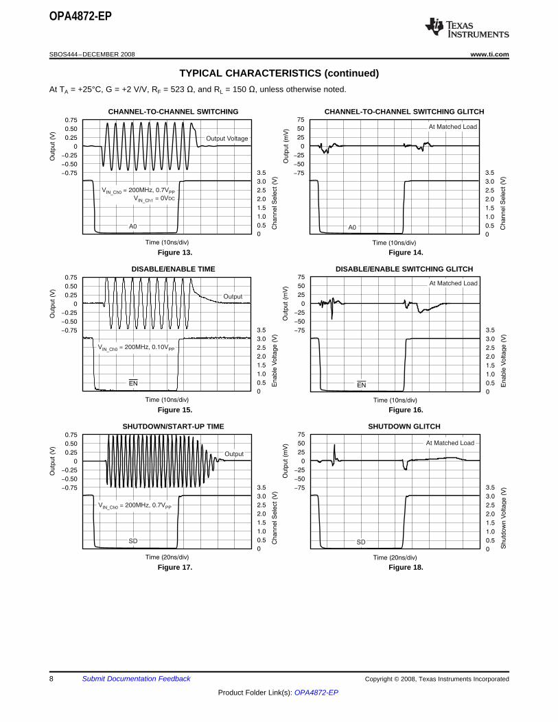
CHANNEL-TO-CHANNEL SWITCHING CHANNEL-TO-CHANNEL SWITCHING GLITCH
Figure 13. Figure 14.
DISABLE/ENABLE TIME DISABLE/ENABLE SWITCHING GLITCH
Figure 15. Figure 16.
SHUTDOWN/START-UP TIME SHUTDOWN GLITCH
Figure 17. Figure 18.
8 Submit Documentation Feedback Copyright © 2008, Texas Instruments Incorporated
Product Folder Link(s): OPA4872-EP

1M
100k
10k
1k
100
10
Frequency (Hz)
10k 100k 1M 10M 100M 1G
Tra
nsim
pe
da
nce
()
W
0
-45
-90
-135
-180
-225
Ph
ase
()°
< ZOL
½ ½ZOL
0
-10
-20
-30
-40
-50
-60
-70
-80
-90
-100
Frequency (Hz)
1M 10M 100M 1G
Cro
ssta
lk (
dB
)
Input-referred
1M
100k
10k
1k
100
10
1
0.1
Frequency (Hz)
100k 1M 10M 100M 1G
Outp
ut Im
pedance (
)W
Disabled (or Shutdown)
Enabled
100M
10M
1M
100k
10k
1k
100
Frequency (Hz)
10k 100k 1M 10M 100M 1G
Input Im
pedance (
)W
Disabled
Enabled
78.00
76.75
75.50
74.25
73.00
71.75
70.50
69.25
68.00
Ambient Temperature ( C)°
-50 -25 0 25 50 75 100 125
Ou
tpu
t C
urr
en
t (m
A)
15.00
13.75
12.50
11.25
10.00
8.75
7.50
6.25
5.00
Su
pp
ly C
urr
en
t (m
A)
Supply Current (I )Q
+IOUT
-IOUT
60
50
40
30
20
10
0
Frequency (Hz)
1k 10k 100k 1M 10M 100M 1G
Pow
er-
Supply
Reje
ction R
atio (
dB
)
-PSRR
+PSRR
Input-referred
OPA4872-EP
www.ti.com........................................................................................................................................................................................... SBOS444–DECEMBER 2008
TYPICAL CHARACTERISTICS (continued)At TA = +25°C, G = +2 V/V, RF = 523 Ω, and RL = 150 Ω, unless otherwise noted.
OPEN-LOOP TRANSIMPEDANCE GAIN AND PHASE vsALL HOSTILE CROSSTALK vs FREQUENCY FREQUENCY
Figure 19. Figure 20.
CLOSED-LOOP OUTPUT IMPEDANCE vs FREQUENCY INPUT IMPEDANCE vs FREQUENCY
Figure 21. Figure 22.
PSRR vs FREQUENCY OUTPUT AND SUPPLY CURRENT vs TEMPERATURE
Figure 23. Figure 24.
Copyright © 2008, Texas Instruments Incorporated Submit Documentation Feedback 9
Product Folder Link(s): OPA4872-EP

2.0
1.5
1.0
0.5
0
-0.5
-1.0
-1.5
-2.0
-2.5
-3.0
Ambient Temperature ( C)°
-50 -25 0 25 50 75 100 125
Ou
tpu
t O
ffse
t V
olta
ge
(m
V)
9
8
7
6
5
4
3
2
1
0
-1
Inp
ut
Bia
s C
urr
en
t (
A)
m
VOS
Ibn
Ibi
300
100
10
1
Frequency (Hz)
10 100 1k 10k 100k 1M 10M
Voltage N
ois
e D
ensity (
nV
/)
ÖH
z
Curr
ent N
ois
e D
ensity (
pA
/)
ÖH
z
Inverting Input Current Noise (19pA/ )HzÖ
Input Voltage Noise (4.5nV/ )ÖHz
Noninverting Input Current Noise (4pA/ )ÖHz
OPA4872-EP
SBOS444–DECEMBER 2008........................................................................................................................................................................................... www.ti.com
TYPICAL CHARACTERISTICS (continued)At TA = +25°C, G = +2 V/V, RF = 523 Ω, and RL = 150 Ω, unless otherwise noted.
TYPICAL DC DRIFT OVER TEMPERATURE INPUT VOLTAGE AND CURRENT NOISE
Figure 25. Figure 26.
10 Submit Documentation Feedback Copyright © 2008, Texas Instruments Incorporated
Product Folder Link(s): OPA4872-EP

APPLICATION INFORMATION
WIDEBAND MULTIPLEXER OPERATION
75W
+5V
-5V
OPA4872
75W
75W
75W
75W
To 75 LoadW523W
523W
IN0
IN1
IN2
IN3
VIN0
VIN1
VIN2
VIN3
A0
A1
SD
EN
VOUT
0.1 Fm
Optional
0.01 Fm 6.8 Fm+
0.1 Fm 6.8 Fm+
OPA4872-EP
www.ti.com........................................................................................................................................................................................... SBOS444–DECEMBER 2008
input of a current feedback amplifier. Depending onthe logic applied to channel control pins A0 and A1,one switch is on at all times. Figure 27 represents the
The OPA4872 gives a new level of performance in OPA4872 in this configuration. The truth table forwideband multiplexers. Figure 27 shows the channel selection is shown in Table 1.dc-coupled, gain of +2 V/V, dual power-supply circuitused as the basis of the ±5-V Electrical Table 1. TRUTH TABLECharacteristics and Typical Characteristic curves. For
A0 A1 EN SD VOUTtest purposes, the input impedance is set to 75 Ω with0 0 0 0 IN0a resistor to ground and the output impedance is set
to 75 Ω with a series output resistor. Voltage swings 1 0 0 0 IN1reported in the specifications are taken directly at the 0 1 0 0 IN2input and output pins while load powers (in dBm) are
1 1 0 0 IN3defined at a matched 75-Ω load. For the circuit ofX X 1 0 High-Z, IQ = 3.4 mAFigure 27, the total effective load will be 150 Ω ||X X X 1 High-Z, IQ = 1.1 mA1046 Ω = 131 Ω. Logic pins A0 and A1 control which
of the four inputs is selected while EN and SD allowThe OPA4872 is in disable mode, with a quiescentfor power reduction. One optional component iscurrent of 3.4mA typical, when the EN pin is set toincluded in Figure 27. In addition to the usual0V. After being placed in disable mode, the OPA4872power-supply decoupling capacitors to ground, ais fully enabled in 6ns. For further power savings, the0.01-µF capacitor is included between the twoSD pin can be used. Setting the SD pin to 5V placespower-supply pins. In practical printed circuit boardthe device in shutdown mode with a standing(PCB) layouts, this optional added capacitor typicallyquiescent current of 1.1 mA. Note that in thisimproves the 2nd-harmonic distortion performance byshutdown mode, the OPA4872 requires 15ns to be3 dB to 6 dB for bipolar supply operation.fully powered again. The truth table for disable and
Even though the internal architecture of the OPA4872 shutdown modes can be found in Table 1.includes current steering, it is advantageous to lookat it as four switches looking into the noninverting
Figure 27. DC-Coupled, G = +2V/V Bipolar Specification and Test Circuit (Channel 0 Selected)
Copyright © 2008, Texas Instruments Incorporated Submit Documentation Feedback 11
Product Folder Link(s): OPA4872-EP
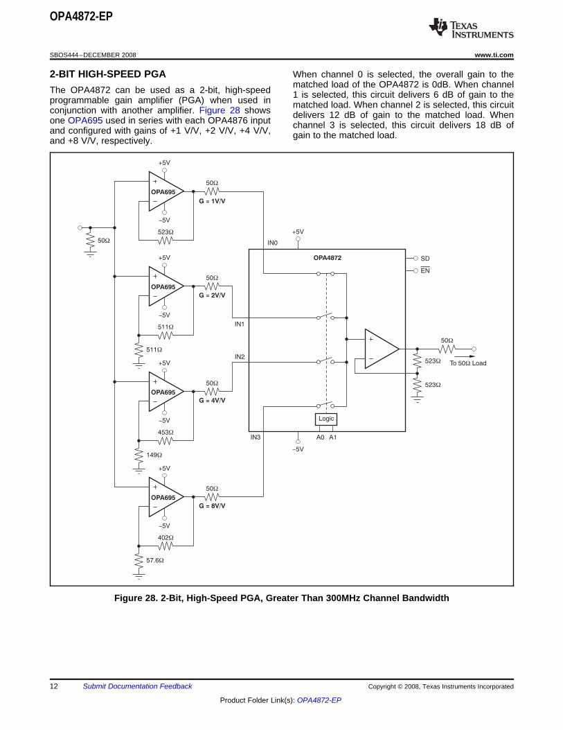
2-BIT HIGH-SPEED PGA
50W
+5V
50W
523W
OPA695
-5V
+5V
50W
511W
511W
OPA695
-5V
+5V
50W
453W
149W
OPA695
-5V
+5V
-5V
+5V
50W
402W
57.6W
OPA4872
OPA695
-5V
50W
To 50 LoadW
Logic
IN0
IN1
IN2
IN3 A0 A1
523W
523W
SD
EN
G = 1V/V
G = 2V/V
G = 4V/V
G = 8V/V
OPA4872-EP
SBOS444–DECEMBER 2008........................................................................................................................................................................................... www.ti.com
When channel 0 is selected, the overall gain to thematched load of the OPA4872 is 0dB. When channelThe OPA4872 can be used as a 2-bit, high-speed 1 is selected, this circuit delivers 6 dB of gain to theprogrammable gain amplifier (PGA) when used in matched load. When channel 2 is selected, this circuitconjunction with another amplifier. Figure 28 shows delivers 12 dB of gain to the matched load. Whenone OPA695 used in series with each OPA4876 input channel 3 is selected, this circuit delivers 18 dB ofand configured with gains of +1 V/V, +2 V/V, +4 V/V, gain to the matched load.and +8 V/V, respectively.
Figure 28. 2-Bit, High-Speed PGA, Greater Than 300MHz Channel Bandwidth
12 Submit Documentation Feedback Copyright © 2008, Texas Instruments Incorporated
Product Folder Link(s): OPA4872-EP
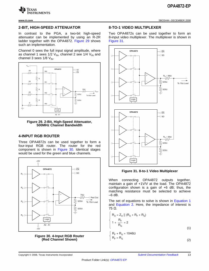
2-BIT, HIGH-SPEED ATTENUATOR 8-TO-1 VIDEO MULTIPLEXER
50W
OPA4872
R
R
R
R
2R
2R
2R
To 50 LoadW523W
523W
IN0
IN1
IN2
IN3
VIN
A0 A1
SD
EN
VOUT
Logic
4-INPUT RGB ROUTER
R = 69WO
OPA4872
To 75 LoadW
Logic
R = 69WO
OPA4872
Logic
523W
523W
523W
523W
EN
SD
EN
SD
R = Z || ( + R + R )O F GO OR
1 + = 2RF
RG(1)
75W
+5V
-5V
OPA4872
To 75 LoadW
Logic
R2
R1
R3
R4
Red Out
A0 A1
523W
523W
EN
SD
R + R = 1046
R = R
WF G
F G (2)
OPA4872-EP
www.ti.com........................................................................................................................................................................................... SBOS444–DECEMBER 2008
In contrast to the PGA, a two-bit high-speed Two OPA4872s can be used together to form anattenuator can be implemented by using an R-2R 8-input video multiplexer. The multiplexer is shown inladder together with the OPA4872. Figure 29 shows Figure 31.such an implementation.
Channel 0 sees the full input signal amplitude, whereas channel 1 sees 1/2 VIN, channel 2 see 1/4 VIN andchannel 3 sees 1/8 VIN.
Figure 29. 2-Bit, High-Speed Attenuator,500MHz Channel Bandwidth
Three OPA4872s can be used together to form afour-input RGB router. The router for the redcomponent is shown in Figure 30. Identical stageswould be used for the green and blue channels.
Figure 31. 8-to-1 Video Multiplexer
When connecting OPA4872 outputs together,maintain a gain of +1V/V at the load. The OPA4872configuration shown is a gain of +6 dB; thus, thematching resistance must be selected to achieve–6 dB.
The set of equations to solve is shown in Equation 1and Equation 2. Here, the impedance of interest is75 Ω.
Figure 30. 4-Input RGB Router(Red Channel Shown)
Copyright © 2008, Texas Instruments Incorporated Submit Documentation Feedback 13
Product Folder Link(s): OPA4872-EP

OPERATING SUGGESTIONS
SETTING RESISTOR VALUES TO OPTIMIZE
R =O2
75 (n 1) + 804´ -
´ 1 +
[75 (n 1) + 804]´ -
2
241200- 1
DESIGN-IN TOOLS
DEMONSTRATION FIXTURERF
VO
RG
RIZ i(S) ERR
iERR
a
VI
MACROMODELS AND APPLICATIONS SUPPORT
OPA4872-EP
SBOS444–DECEMBER 2008........................................................................................................................................................................................... www.ti.com
Solving for RO, with n devices connected together,results in Equation 3:
BANDWIDTHThe output stage of the OPA4872 is acurrent-feedback op amp, meaning it can hold analmost constant bandwidth over signal gain settings(3)with the proper adjustment of the external resistor
Results for n varying from 2 to 6 are given in Table 2. values. This performance is shown in the TypicalCharacteristic curves; the small-signal bandwidth
Table 2. Series Resistance vs decreases only slightly with increasing gain. TheseNumber of Parallel Outputs curves also show that the feedback resistor has been
changed for each gain setting. The resistor values onNUMBER OF OPA4872s RO (Ω)the feedback path can be treated as frequency2 69response compensation elements while the ratio sets
3 63.94 the signal gain of the feedback resistor divided by the4 59.49 gain resistor. Figure 32 shows the small-signal5 55.59 frequency response analysis circuit for a current
feedback amplifier.6 52.15
The two major limitations of this circuit are the devicerequirements for each OPA4872 and the acceptablereturn loss resulting from the mismatch between theload and the matching resistor.
A printed circuit board (PCB) is available to assist inthe initial evaluation of circuit performance using theOPA4872. The fixture is offered free of charge as anunpopulated PCB, delivered with a user's guide. Thesummary information for this fixture is shown inTable 3.
Figure 32. Recommended Feedback Resistor vsNoise GainTable 3. OPA4872 Demonstration Fixture
LITERATUREPACKAGE ORDERING NUMBER NUMBER The key elements of this current-feedback op amp
model are:SO-14 DEM-OPA-SO-1E SBOU045
α → Buffer gain from the noninverting input to theThe demonstration fixture can be requested at the inverting inputTexas Instruments web site at (www.ti.com) throughthe OPA4872 product folder. RI → Buffer output impedance
iERR → Feedback error current signal
Z(s) → Frequency-dependent open-loopComputer simulation of circuit performance usingtransimpedance gain from iERR to VOSPICE is often useful when analyzing the
performance of analog circuits and systems. This The buffer gain is typically very close to 1.00 and ispractice is particularly true for video and RF amplifier normally neglected from signal gain considerations. Itcircuits, where parasitic capacitance and inductance will, however, set the CMRR for a single op ampcan have a major effect on circuit performance. A differential amplifier configuration. For a buffer gainSPICE model for the OPA4872 is available through α < 1.0, the CMRR = –20 × log (1 – α) dB.the Texas Instruments web site at www.ti.com. Thismodel does a good job of predicting small-signal acand transient performance under a wide variety ofoperating conditions. It does not do as well inpredicting the harmonic distortion or dG/dPcharacteristics.
14 Submit Documentation Feedback Copyright © 2008, Texas Instruments Incorporated
Product Folder Link(s): OPA4872-EP

R = 663 NG x RW -F I (6)
VO
VI
= =
R R+F I 1+
Z(S)
1+
RF
RG
a
R R NG+F I
Z(S)
1+
aNG1+
RF
RG
NG = 1+R
F
RG (4)
= Loop GainZ(S)
R + RF I NG (5)
600
550
500
450
400
350
300
250
200
150
100
Noise Gain
0 2010 155
Feedback R
esis
tor
()
W
OPA4872-EP
www.ti.com........................................................................................................................................................................................... SBOS444–DECEMBER 2008
RI, the buffer output impedance, is a critical portion of The OPA4872 is internally compensated to give athe bandwidth control equation. RI for the OPA4872 is maximally flat frequency response for RF = 523 Ω attypically about 30 Ω. A current-feedback op amp NG = 2 on ±5-V supplies. Evaluating the denominatorsenses an error current in the inverting node (as of Equation 5 (which is the feedback transimpedance)opposed to a differential input error voltage for a gives an optimal target of 663 Ω. As the signal gainvoltage-feedback op amp) and passes this on to the changes, the contribution of the NG × RI term in theoutput through an internal frequency dependent feedback transimpedance will change, but the totaltransimpedance gain. The Typical Characteristics can be held constant by adjusting RF. Equation 6show this open-loop transimpedance response. This gives an approximate equation for optimum RF overopen-loop response is analogous to the open-loop signal gain:voltage gain curve for a voltage-feedback op amp.Developing the transfer function for the circuit ofFigure 32 gives Equation 4: As the desired signal gain increases, this equation
will eventually predict a negative RF. A somewhatsubjective limit to this adjustment also can be set byholding RG to a minimum value of 20 Ω. Lower valuesload both the buffer stage at the input and the outputstage, if RF gets too low, actually decreasing thebandwidth. Figure 33 shows the recommended RFversus NG for ±5-V operation. The values for RFversus gain shown here are approximately equal to
where: the values used to generate the TypicalCharacteristics. They differ in that the optimizedvalues used in the Typical Characteristics are alsocorrecting for board parasitics not considered in thesimplified analysis leading to Equation 5. The valuesThis formula is written in a loop-gain analysis format,shown in Figure 33 give a good starting point forwhere the errors arising from a noninfinite open-loopdesign where bandwidth optimization is desired.gain are shown in the denominator. If Z(S) were
infinite over all frequencies, the denominator ofEquation 4 would reduce to 1 and the ideal desiredsignal gain shown in the numerator would beachieved. The fraction in the denominator ofEquation 4 determines the frequency response.Equation 5 shows this as the loop-gain equation:
If 20 × log(RF + NG × RI) were drawn on top of theopen-loop transimpedance plot, the differencebetween the two calculations would be the loop gainat a given frequency. Eventually, Z(S) rolls off to equalthe denominator of Equation 5, at which point theloop gain reduces to 1 (and the curves intersect).This point of equality is where the amplifier
Figure 33. Feedback Resistor vs Noise Gainclosed-loop frequency response given by Equation 4starts to roll off, and is exactly analogous to thefrequency at which the noise gain equals the The total impedance going into the inverting inputopen-loop voltage gain for a voltage-feedback op may be used to adjust the closed-loop signalamp. The difference here is that the total impedance bandwidth. Inserting a series resistor between thein the denominator of Equation 5 may be controlled inverting input and the summing junction increasessomewhat separately from the desired signal gain (or the feedback impedance (denominator of Equation 4),NG). decreasing the bandwidth.
Copyright © 2008, Texas Instruments Incorporated Submit Documentation Feedback 15
Product Folder Link(s): OPA4872-EP

DRIVING CAPACITIVE LOADS V = V (R I ) G´OSO_envelope OS S b´ ´G I x Rbi F± ±
±½- - ½ ´5 (V ) 10S--
PSRR-
20
± ½ -5 (V ) 10S+ ½ ´ -PSRR+
20
(7)
±½- - - ½ ´5 ( 6) 10-
51
20
50
20±½ - ½ ´5 6 10-
= 29.2mV±
+523 18 AW ´ ± m
± ´ ± ´10mV + 75 14 A 2W m
(8)
DISTORTION PERFORMANCE
DC ACCURACY
OPA4872-EP
SBOS444–DECEMBER 2008........................................................................................................................................................................................... www.ti.com
One of the most demanding, yet very common loadconditions, is capacitive loading. Often, the capacitiveload is the input of an analog-to-digital converter(ADC)—including additional external capacitance that
Where:may be recommended to improve ADC linearity. ARS: Input resistance seen by R0, R1, G0, G1, B0,high-speed device such as the OPA4872 can be veryor B1.susceptible to decreased stability and closed-loop
response peaking when a capacitive load is placed Ib: Noninverting input bias currentdirectly on the output pin. When the device open-loop Ibi: Inverting input bias currentoutput resistance is considered, this capacitive load G: Gainintroduces an additional pole in the signal path that
VS+: Positive supply voltagecan decrease the phase margin. Several externalsolutions to this problem have been suggested. When VS–: Negative supply voltagethe primary considerations are frequency response PSRR+: Positive supply PSRRflatness, pulse response fidelity, and/or distortion, the PSRR–: Negative supply PSRRsimplest and most effective solution is to isolate the
VOS: Input Offset Voltagecapacitive load from the feedback loop by inserting aseries isolation resistor between the amplifier output Evaluating the front-page schematic, using aand the capacitive load. This isolation resistor does worst-case, +25°C offset voltage, bias current andnot eliminate the pole from the loop response, but PSRR specifications and operating at ±6 V, gives arather shifts it and adds a zero at a higher frequency. worst-case output equal to Equation 8:The additional zero acts to cancel the phase lag fromthe capacitive load pole, thus increasing the phasemargin and improving stability.
The Typical Characteristics show the recommendedRS versus capacitive load and the resulting frequencyresponse at the load; see Figure 5. Parasiticcapacitive loads greater than 2 pF can begin todegrade the performance of the OPA4872. Long PCB
The OPA4872 provides good distortion performancetraces, unmatched cables, and connections tointo a 150-Ω load on ±5-V supplies. Relative tomultiple devices can easily cause this value to bealternative solutions, it provides exceptionalexceeded. Always consider this effect carefully, andperformance into lighter loads. Generally, until theadd the recommended series resistor as close asfundamental signal reaches very high frequency orpossible to the OPA4872 output pin (see the Boardpower levels, the 2nd harmonic dominates theLayout Guidelines section).distortion with a negligible 3rd harmonic component.Focusing then on the 2nd harmonic, increasing theload impedance directly improves distortion. Also,The OPA4872 offers excellent dc signal accuracy. providing an additional supply decoupling capacitorParameters that influence the output dc offset voltage (0.01 µF) between the supply pins (for bipolarare: operation) improves the 2nd-order distortion slightly
• Output offset voltage (3 dB to 6 dB).• Input bias current In most op amps, increasing the output voltage swing• Gain error increases harmonic distortion directly. The Typical• Power-supply rejection ratio Characteristics show the 2nd harmonic increasing at
a little less than the expected 2X rate while the 3rd• Temperatureharmonic increases at a little less than the expected3X rate. Where the test power doubles, the 2ndLeaving both temperature and gain error parametersharmonic increases only by less than the expected 6aside, the output offset voltage envelope can bedB, whereas the 3rd harmonic increases by less thandescribed as shown in Equation 7:the expected 12 dB.
16 Submit Documentation Feedback Copyright © 2008, Texas Instruments Incorporated
Product Folder Link(s): OPA4872-EP

NOISE PERFORMANCEE =O E + (I R ) + 4kTRNI BN S S NG +
2 22(I R )BI F + 4kTR NGFÖ( 2)
E =O E + (I R ) + 4kTRNI BN S S +2 2 I RBI F
NG
4kTRF
NG+Ö )(2
(10)
4kT
RG
RG
RF
RS
OPA4872
IBI
EO
IBN
4kT = 1.6 10 Jx- 20
at 290K
ERS
ENI
Ö4kTRF
Ö4kTRS
OPA4872-EP
www.ti.com........................................................................................................................................................................................... SBOS444–DECEMBER 2008
The OPA4872 offers an excellent balance between(9)voltage and current noise terms to achieve low output
noise. The inverting current noise (19 pA/√Hz) is Dividing this expression by the noise gain (NG = (1 +significantly lower than earlier solutions, while the RF/RG)) gives the equivalent input-referred spot noiseinput voltage noise (4.5 nV/√Hz) is lower than most voltage at the noninverting input, as shown inunity-gain stable, wideband, voltage-feedback op Equation 10.amps. As long as the ac source impedance lookingout of the noninverting node is less than 100 Ω, thiscurrent noise will not contribute significantly to thetotal output noise. The op amp input voltage noise
Evaluating these two equations for the OPA4872and the two input current noise terms combine to givecircuit and component values (see Figure 27) gives alow output noise under a wide variety of operatingtotal output spot noise voltage of 14.2 nV/√Hz and aconditions. Figure 34 shows the OPA4872 noisetotal equivalent input spot noise voltage of 7.1analysis model with all the noise terms included. InnV/√Hz. This total input-referred spot noise voltage isthis model, all noise terms are taken to be noisehigher than the 4.5-nV/√Hz specification for thevoltage or current density terms in either nV/√Hz orOPA4872 voltage noise alone. This voltage reflectspA/√Hz.the noise added to the output by the inverting currentnoise times the feedback resistor. If the feedbackresistor is reduced in high-gain configurations, thetotal input-referred voltage noise given byEquation 10 approaches only the 4.5 nV/√Hz of theop amp itself. For example, going to a gain of +10using RF = 178 Ω gives a total input-referred noise of4.7 nV/√Hz.
Figure 34. Op Amp Noise Analysis Model
The total output spot noise voltage can be computedas the square root of the sum of all squared outputnoise voltage contributors. Equation 9 shows thegeneral form for the output noise voltage using theterms shown in Figure 35.
Copyright © 2008, Texas Instruments Incorporated Submit Documentation Feedback 17
Product Folder Link(s): OPA4872-EP

THERMAL ANALYSIS
4kT = 1.6 x 10 J
at 290K
-20
4kT
VRF
= 4kTRF
Ö
OPA4872e
n
ini
iin
RS
VRS
= 4kTRS
Ö
RG
eo
RF
iRG R
GÖ
OPA4872-EP
SBOS444–DECEMBER 2008........................................................................................................................................................................................... www.ti.com
load power. Quiescent power is simply the specifiedno-load supply current times the total supply voltageHeatsinking or forced airflow may be required under across the part. PDL depends on the required outputextreme operating conditions. Maximum desired signal and load; for a grounded resistive load, PDL isjunction temperature sets the maximum allowed at a maximum when the output is fixed at a voltageinternal power dissipation as discussed in this equal to 1/2 of either supply voltage (for equal bipolardocument. In no case should the maximum junction supplies). Under this condition PDL = VS
2/(4 × RL),temperature be allowed to exceed +150°C. where RL includes feedback network loading.Operating junction temperature (TJ) is given by TA + Note that it is the power in the output stage and not inPD × θJA. The total internal power dissipation (PD) is the load that determines internal power dissipation.the sum of quiescent power (PDQ) and additionalpower dissipated in the output stage (PDL) to deliver
Figure 35. OPA4872 Noise Analysis Model
18 Submit Documentation Feedback Copyright © 2008, Texas Instruments Incorporated
Product Folder Link(s): OPA4872-EP

P = 10V 11.7mA + 5 /[4 (150 || 1046 )] = 165mW´ W( )D ´ W2
Maximum T = +85 C + (165mW 80 C/W) = 98 C° ´J ° °
BOARD LAYOUT GUIDELINES
OPA4872-EP
www.ti.com........................................................................................................................................................................................... SBOS444–DECEMBER 2008
As a worst-case example, compute the maximum TJ Again, keep their leads and PCB trace length as shortusing an OPA4872ID in the circuit of Figure 27 as possible. Never use wirewound type resistors in aoperating at the maximum specified ambient high-frequency application. Other networktemperature of +85°C with its output driving a components, such as noninverting input terminationgrounded 100-Ω load to +2.5 V: resistors, should also be placed close to the package.
d) Connections to other wideband devices on theboard may be made with short direct traces orthrough onboard transmission lines. For shortconnections, consider the trace and the input to thenext device as a lumped capacitive load. RelativelyThis worst-case condition does not exceed thewide traces (50mils to 100mils) should be used,maximum junction temperature. Normally, thispreferably with ground and power planes opened upextreme case is not encountered.around them.
Estimate the total capacitive load and set RS from theplot of Figure 5. Low parasitic capacitive loadsAchieving optimum performance with a(greater than 5 pF) may not need an RS because thehigh-frequency amplifier such as the OPA4872OPA4872 is nominally compensated to operate with arequires careful attention to board layout parasitics2-pF parasitic load. If a long trace is required, and theand external component types. Recommendations to6dB signal loss intrinsic to a doubly-terminatedoptimize performance include:transmission line is acceptable, implement a matched
a) Minimize parasitic capacitance to any ac impedance transmission line using microstrip orground for all of the signal I/O pins. Parasitic stripline techniques (consult an ECL design handbookcapacitance on the output pin can cause instability; for microstrip and stripline layout techniques). A 50-Ωon the noninverting input, it can react with the source environment is normally not necessary on the board,impedance to cause unintentional bandlimiting. To and in fact, a higher impedance environmentreduce unwanted capacitance, a window around the improves distortion as shown in the Distortion versussignal I/O pins should be opened in all of the ground Load plot; see Figure 7. With a characteristic boardand power planes around those pins. Otherwise, trace impedance defined based on board materialground and power planes should be unbroken and trace dimensions, a matching series resistor intoelsewhere on the board. the trace from the output of the OPA4872 is used as
well as a terminating shunt resistor at the input of theb) Minimize the distance (< 0.25") from the destination device. Remember also that thepower-supply pins to high frequency 0.1-µF terminating impedance is the parallel combination ofdecoupling capacitors. At the device pins, the the shunt resistor and the input impedance of theground and power plane layout should not be in close destination device; this total effective impedanceproximity to the signal I/O pins. Avoid narrow power should be set to match the trace impedance. Theand ground traces to minimize inductance between high output voltage and current capability of thethe pins and the decoupling capacitors. The OPA4872 allow multiple destination devices to bepower-supply connections (on pins 9, 11, 13, and 15) handled as separate transmission lines, each with itsshould always be decoupled with these capacitors. own series and shunt terminations. If the 6-dBAn optional supply decoupling capacitor across the attenuation of a doubly-terminated transmission linetwo power supplies (for bipolar operation) improves is unacceptable, a long trace can be2nd harmonic distortion performance. Larger (2.2 µF series-terminated at the source end only. Treat theto 6.8 µF) decoupling capacitors, effective at lower trace as a capacitive load in this case and set thefrequency, should also be used on the main supply series resistor value as shown in Figure 5. Thispins. These capacitors may be placed somewhat configuration does not preserve signal integrity asfarther from the device and may be shared among well as a doubly-terminated line. If the inputseveral devices in the same area of the PCB. impedance of the destination device is low, there willc) Careful selection and placement of external be some signal attenuation because of the voltagecomponents preserves the high-frequency divider formed by the series output into theperformance of the OPA4872. Resistors should be terminating impedance.a very low reactance type. Surface-mount resistorswork best and allow a tighter overall layout. Metal-filmand carbon composition, axially-leaded resistors canalso provide good high-frequency performance.
Copyright © 2008, Texas Instruments Incorporated Submit Documentation Feedback 19
Product Folder Link(s): OPA4872-EP

ExternalPin
+VCC
-VCC
InternalCircuitry
INPUT AND ESD PROTECTION
OPA4872-EP
SBOS444–DECEMBER 2008........................................................................................................................................................................................... www.ti.com
e) Socketing a high-speed part like the OPA4872is not recommended. The additional lead length andpin-to-pin capacitance introduced by the socket cancreate an extremely troublesome parasitic networkthat can make it almost impossible to achieve asmooth, stable frequency response. Best results areobtained by soldering the OPA4872 onto the board.
Figure 36. Internal ESD ProtectionThe OPA4872 is built using a very high-speedcomplementary bipolar process. The internal junction These diodes provide moderate protection to inputbreakdown voltages are relatively low for these very overdrive voltages above the supplies as well. Thesmall geometry devices. These breakdowns are protection diodes can typically support 30-mAreflected in the Absolute Maximum Ratings table. All continuous current. Where higher currents aredevice pins have limited ESD protection using internal possible (for example, in systems with ±15-V supplydiodes to the power supplies as shown in Figure 36. parts driving into the OPA4872), current-limiting
series resistors should be added into the two inputs.Keep these resistor values as low as possiblebecause high values degrade both noise performanceand frequency response.
20 Submit Documentation Feedback Copyright © 2008, Texas Instruments Incorporated
Product Folder Link(s): OPA4872-EP

TAPE AND REEL INFORMATION
*All dimensions are nominal
Device PackageType
PackageDrawing
Pins SPQ ReelDiameter
(mm)
ReelWidth
W1 (mm)
A0(mm)
B0(mm)
K0(mm)
P1(mm)
W(mm)
Pin1Quadrant
OPA4872MDREP SOIC D 14 2500 330.0 16.4 6.5 9.0 2.1 8.0 16.0 Q1
PACKAGE MATERIALS INFORMATION
www.ti.com 14-Jul-2012
Pack Materials-Page 1

*All dimensions are nominal
Device Package Type Package Drawing Pins SPQ Length (mm) Width (mm) Height (mm)
OPA4872MDREP SOIC D 14 2500 367.0 367.0 38.0
PACKAGE MATERIALS INFORMATION
www.ti.com 14-Jul-2012
Pack Materials-Page 2


IMPORTANT NOTICE
Texas Instruments Incorporated and its subsidiaries (TI) reserve the right to make corrections, enhancements, improvements and otherchanges to its semiconductor products and services per JESD46C and to discontinue any product or service per JESD48B. Buyers shouldobtain the latest relevant information before placing orders and should verify that such information is current and complete. Allsemiconductor products (also referred to herein as “components”) are sold subject to TI’s terms and conditions of sale supplied at the timeof order acknowledgment.
TI warrants performance of its components to the specifications applicable at the time of sale, in accordance with the warranty in TI’s termsand conditions of sale of semiconductor products. Testing and other quality control techniques are used to the extent TI deems necessaryto support this warranty. Except where mandated by applicable law, testing of all parameters of each component is not necessarilyperformed.
TI assumes no liability for applications assistance or the design of Buyers’ products. Buyers are responsible for their products andapplications using TI components. To minimize the risks associated with Buyers’ products and applications, Buyers should provideadequate design and operating safeguards.
TI does not warrant or represent that any license, either express or implied, is granted under any patent right, copyright, mask work right, orother intellectual property right relating to any combination, machine, or process in which TI components or services are used. Informationpublished by TI regarding third-party products or services does not constitute a license to use such products or services or a warranty orendorsement thereof. Use of such information may require a license from a third party under the patents or other intellectual property of thethird party, or a license from TI under the patents or other intellectual property of TI.
Reproduction of significant portions of TI information in TI data books or data sheets is permissible only if reproduction is without alterationand is accompanied by all associated warranties, conditions, limitations, and notices. TI is not responsible or liable for such altereddocumentation. Information of third parties may be subject to additional restrictions.
Resale of TI components or services with statements different from or beyond the parameters stated by TI for that component or servicevoids all express and any implied warranties for the associated TI component or service and is an unfair and deceptive business practice.TI is not responsible or liable for any such statements.
Buyer acknowledges and agrees that it is solely responsible for compliance with all legal, regulatory and safety-related requirementsconcerning its products, and any use of TI components in its applications, notwithstanding any applications-related information or supportthat may be provided by TI. Buyer represents and agrees that it has all the necessary expertise to create and implement safeguards whichanticipate dangerous consequences of failures, monitor failures and their consequences, lessen the likelihood of failures that might causeharm and take appropriate remedial actions. Buyer will fully indemnify TI and its representatives against any damages arising out of the useof any TI components in safety-critical applications.
In some cases, TI components may be promoted specifically to facilitate safety-related applications. With such components, TI’s goal is tohelp enable customers to design and create their own end-product solutions that meet applicable functional safety standards andrequirements. Nonetheless, such components are subject to these terms.
No TI components are authorized for use in FDA Class III (or similar life-critical medical equipment) unless authorized officers of the partieshave executed a special agreement specifically governing such use.
Only those TI components which TI has specifically designated as military grade or “enhanced plastic” are designed and intended for use inmilitary/aerospace applications or environments. Buyer acknowledges and agrees that any military or aerospace use of TI componentswhich have not been so designated is solely at the Buyer's risk, and that Buyer is solely responsible for compliance with all legal andregulatory requirements in connection with such use.
TI has specifically designated certain components which meet ISO/TS16949 requirements, mainly for automotive use. Components whichhave not been so designated are neither designed nor intended for automotive use; and TI will not be responsible for any failure of suchcomponents to meet such requirements.
Products Applications
Audio www.ti.com/audio Automotive and Transportation www.ti.com/automotive
Amplifiers amplifier.ti.com Communications and Telecom www.ti.com/communications
Data Converters dataconverter.ti.com Computers and Peripherals www.ti.com/computers
DLP® Products www.dlp.com Consumer Electronics www.ti.com/consumer-apps
DSP dsp.ti.com Energy and Lighting www.ti.com/energy
Clocks and Timers www.ti.com/clocks Industrial www.ti.com/industrial
Interface interface.ti.com Medical www.ti.com/medical
Logic logic.ti.com Security www.ti.com/security
Power Mgmt power.ti.com Space, Avionics and Defense www.ti.com/space-avionics-defense
Microcontrollers microcontroller.ti.com Video and Imaging www.ti.com/video
RFID www.ti-rfid.com
OMAP Mobile Processors www.ti.com/omap TI E2E Community e2e.ti.com
Wireless Connectivity www.ti.com/wirelessconnectivity
Mailing Address: Texas Instruments, Post Office Box 655303, Dallas, Texas 75265Copyright © 2012, Texas Instruments Incorporated