![core.ac.uk fileTERHADAP PENCEGAHAN FRAUD Rusman Soleman THE DETERMINANTS OF CORPORATE COMMUNITY CONTRIBUTIONS: ... pita], either medical people or supporting peo- ple, ...](https://static.fdocuments.net/doc/165x107/5cc2c1ae88c99389538b7d0f/coreacuk-pencegahan-fraud-rusman-soleman-the-determinants-of-corporate-community.jpg)
Supporting Information whwang - rsc.org · Electronic Supporting Information (ESI) PEO-coated...
7
Electronic Supporting Information (ESI) PEO-coated nanoporous alumina The PEO-coated nanochannel arrays were fabricated by two-step anodization and one- step PEO coating method (see Supporting imformation, Figure S1). A pure Al sheet (99.999 %), 1mm thick, was electropolished in a mixture of perchloric acid and ethanol (HClO4:C2H5OH = 1:4 volumetric ratio) in order to remove surface irregularities, at a constant voltage of 20V and temperature of 7°C. Highly ordered porous aluminum oxide was obtained from two-step anodization (0.3 M sulfuric acid, 0°C, 25 V). The pore size of the aluminum oxide was simply adjusted by etching in a 0.1M phosphoric acid solution at 30°C (see Supporting information, Figure S2). FE-SEM was performed using JEOL JSM-7401F (NCNT). The aluminum layer was removed in a CuCl 2 -based solution (100ml of HCl (38 %) + 100 ml H 2 O + 3.4 g of CuCl 2 ·H 2 O) at room temperature for about 10min. The alumina barrier layer was etched in 0.1 M phosphoric acid at 30°C for 70 min. After detachment of the nanoporous membrane using 0.1 M phosphoric acid for 60 min, a PEO monolayer formed on the nanoporous membrane surface in 2 mM solution of Cl 3 SiPEO in toluene at room temperature for 24 hr. Figure S1. Steps in the fabrication of the PEO-coated nanochannel array. Supplementary Material (ESI) for Lab on a Chip This journal is © The Royal Society of Chemistry 2011
Transcript of Supporting Information whwang - rsc.org · Electronic Supporting Information (ESI) PEO-coated...
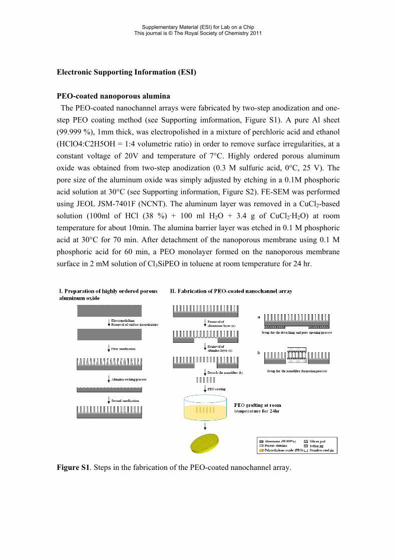
Electronic Supporting Information (ESI) PEO-coated nanoporous alumina The PEO-coated nanochannel arrays were fabricated by two-step anodization and one-
step PEO coating method (see Supporting imformation, Figure S1). A pure Al sheet (99.999 %), 1mm thick, was electropolished in a mixture of perchloric acid and ethanol (HClO4:C2H5OH = 1:4 volumetric ratio) in order to remove surface irregularities, at a constant voltage of 20V and temperature of 7°C. Highly ordered porous aluminum oxide was obtained from two-step anodization (0.3 M sulfuric acid, 0°C, 25 V). The pore size of the aluminum oxide was simply adjusted by etching in a 0.1M phosphoric acid solution at 30°C (see Supporting information, Figure S2). FE-SEM was performed using JEOL JSM-7401F (NCNT). The aluminum layer was removed in a CuCl2-based solution (100ml of HCl (38 %) + 100 ml H2O + 3.4 g of CuCl2·H2O) at room temperature for about 10min. The alumina barrier layer was etched in 0.1 M phosphoric acid at 30°C for 70 min. After detachment of the nanoporous membrane using 0.1 M phosphoric acid for 60 min, a PEO monolayer formed on the nanoporous membrane surface in 2 mM solution of Cl3SiPEO in toluene at room temperature for 24 hr.
Figure S1. Steps in the fabrication of the PEO-coated nanochannel array.
Supplementary Material (ESI) for Lab on a ChipThis journal is © The Royal Society of Chemistry 2011
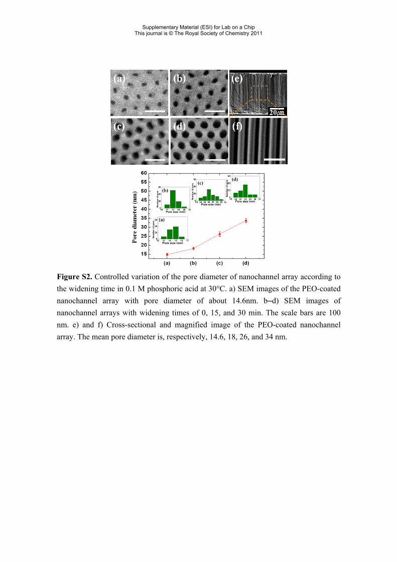
Figure S2. Controlled variation of the pore diameter of nanochannel array according to the widening time in 0.1 M phosphoric acid at 30°C. a) SEM images of the PEO-coated nanochannel array with pore diameter of about 14.6nm. b–d) SEM images of nanochannel arrays with widening times of 0, 15, and 30 min. The scale bars are 100 nm. e) and f) Cross-sectional and magnified image of the PEO-coated nanochannel array. The mean pore diameter is, respectively, 14.6, 18, 26, and 34 nm.
Supplementary Material (ESI) for Lab on a ChipThis journal is © The Royal Society of Chemistry 2011
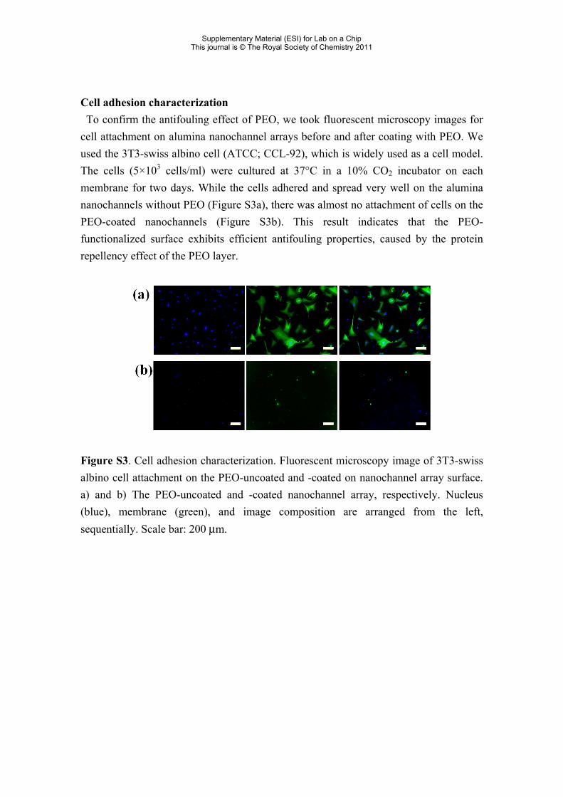
Cell adhesion characterization To confirm the antifouling effect of PEO, we took fluorescent microscopy images for
cell attachment on alumina nanochannel arrays before and after coating with PEO. We used the 3T3-swiss albino cell (ATCC; CCL-92), which is widely used as a cell model. The cells (5×10³ cells/ml) were cultured at 37°C in a 10% CO2 incubator on each membrane for two days. While the cells adhered and spread very well on the alumina nanochannels without PEO (Figure S3a), there was almost no attachment of cells on the PEO-coated nanochannels (Figure S3b). This result indicates that the PEO-functionalized surface exhibits efficient antifouling properties, caused by the protein repellency effect of the PEO layer.
Figure S3. Cell adhesion characterization. Fluorescent microscopy image of 3T3-swiss albino cell attachment on the PEO-uncoated and -coated on nanochannel array surface. a) and b) The PEO-uncoated and -coated nanochannel array, respectively. Nucleus (blue), membrane (green), and image composition are arranged from the left, sequentially. Scale bar: 200 μm.
Supplementary Material (ESI) for Lab on a ChipThis journal is © The Royal Society of Chemistry 2011
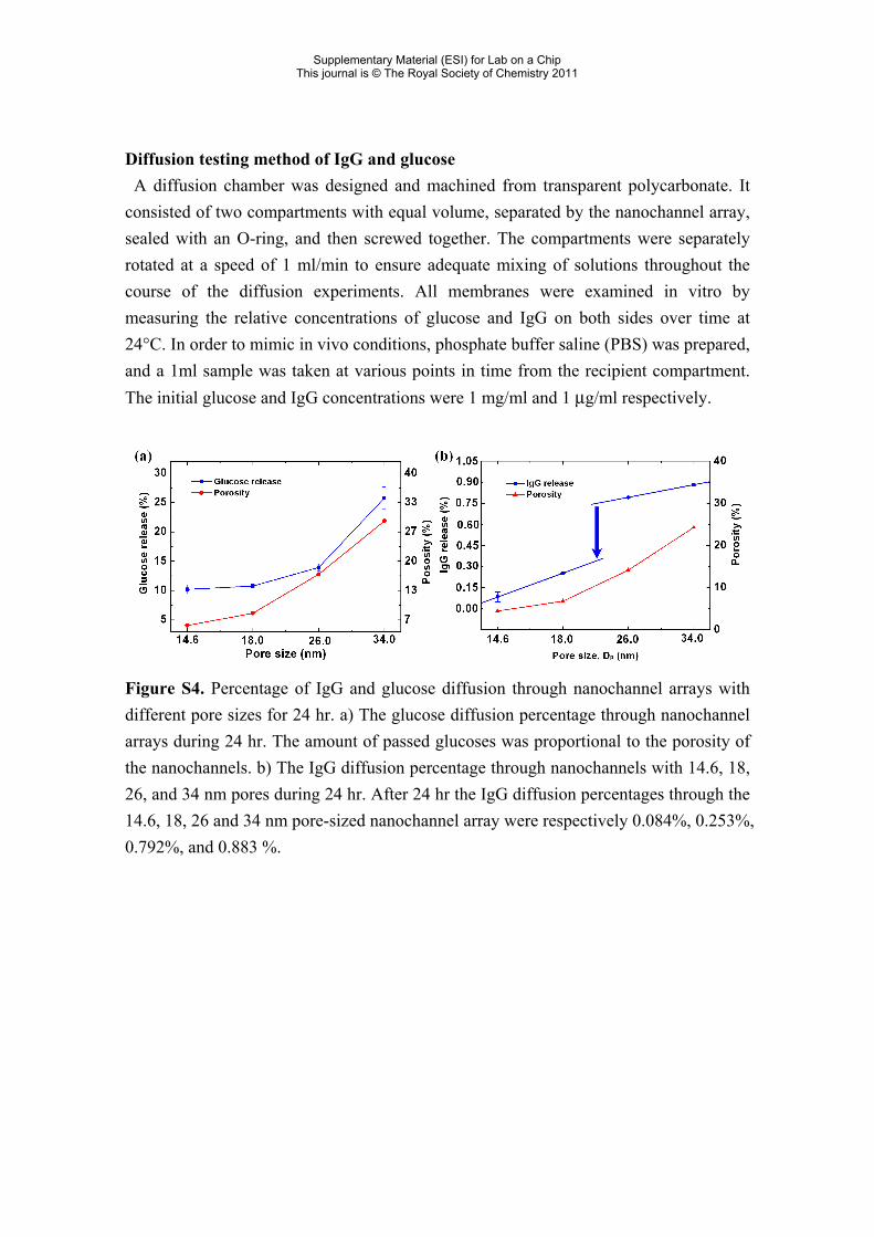
Diffusion testing method of IgG and glucose A diffusion chamber was designed and machined from transparent polycarbonate. It
consisted of two compartments with equal volume, separated by the nanochannel array, sealed with an O-ring, and then screwed together. The compartments were separately rotated at a speed of 1 ml/min to ensure adequate mixing of solutions throughout the course of the diffusion experiments. All membranes were examined in vitro by measuring the relative concentrations of glucose and IgG on both sides over time at 24°C. In order to mimic in vivo conditions, phosphate buffer saline (PBS) was prepared, and a 1ml sample was taken at various points in time from the recipient compartment. The initial glucose and IgG concentrations were 1 mg/ml and 1 μg/ml respectively.
Figure S4. Percentage of IgG and glucose diffusion through nanochannel arrays with different pore sizes for 24 hr. a) The glucose diffusion percentage through nanochannel arrays during 24 hr. The amount of passed glucoses was proportional to the porosity of the nanochannels. b) The IgG diffusion percentage through nanochannels with 14.6, 18, 26, and 34 nm pores during 24 hr. After 24 hr the IgG diffusion percentages through the 14.6, 18, 26 and 34 nm pore-sized nanochannel array were respectively 0.084%, 0.253%, 0.792%, and 0.883 %.
Supplementary Material (ESI) for Lab on a ChipThis journal is © The Royal Society of Chemistry 2011
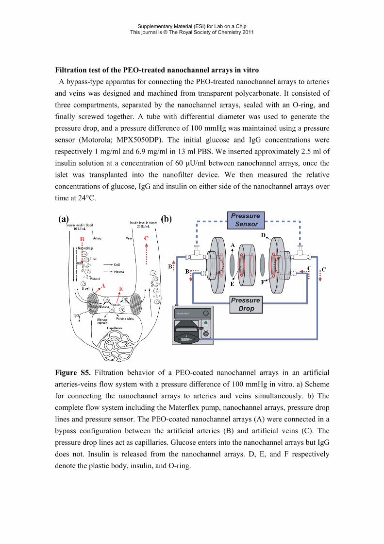
Filtration test of the PEO-treated nanochannel arrays in vitro A bypass-type apparatus for connecting the PEO-treated nanochannel arrays to arteries
and veins was designed and machined from transparent polycarbonate. It consisted of three compartments, separated by the nanochannel arrays, sealed with an O-ring, and finally screwed together. A tube with differential diameter was used to generate the pressure drop, and a pressure difference of 100 mmHg was maintained using a pressure sensor (Motorola; MPX5050DP). The initial glucose and IgG concentrations were respectively 1 mg/ml and 6.9 mg/ml in 13 ml PBS. We inserted approximately 2.5 ml of insulin solution at a concentration of 60 μU/ml between nanochannel arrays, once the islet was transplanted into the nanofilter device. We then measured the relative concentrations of glucose, IgG and insulin on either side of the nanochannel arrays over time at 24°C.
Figure S5. Filtration behavior of a PEO-coated nanochannel arrays in an artificial arteries-veins flow system with a pressure difference of 100 mmHg in vitro. a) Scheme for connecting the nanochannel arrays to arteries and veins simultaneously. b) The complete flow system including the Materflex pump, nanochannel arrays, pressure drop lines and pressure sensor. The PEO-coated nanochannel arrays (A) were connected in a bypass configuration between the artificial arteries (B) and artificial veins (C). The pressure drop lines act as capillaries. Glucose enters into the nanochannel arrays but IgG does not. Insulin is released from the nanochannel arrays. D, E, and F respectively denote the plastic body, insulin, and O-ring.
Supplementary Material (ESI) for Lab on a ChipThis journal is © The Royal Society of Chemistry 2011
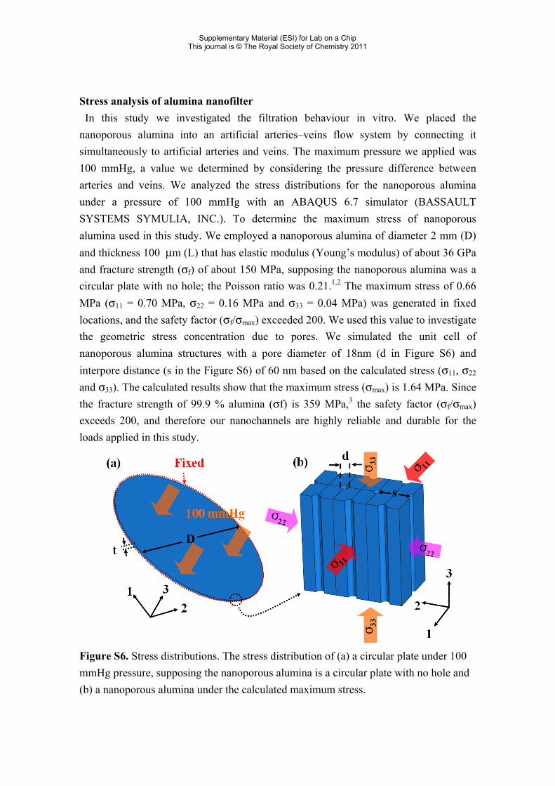
Stress analysis of alumina nanofilter In this study we investigated the filtration behaviour in vitro. We placed the
nanoporous alumina into an artificial arteries–veins flow system by connecting it simultaneously to artificial arteries and veins. The maximum pressure we applied was 100 mmHg, a value we determined by considering the pressure difference between arteries and veins. We analyzed the stress distributions for the nanoporous alumina under a pressure of 100 mmHg with an ABAQUS 6.7 simulator (BASSAULT SYSTEMS SYMULIA, INC.). To determine the maximum stress of nanoporous alumina used in this study. We employed a nanoporous alumina of diameter 2 mm (D) and thickness 100 μm (L) that has elastic modulus (Young’s modulus) of about 36 GPa and fracture strength (σf) of about 150 MPa, supposing the nanoporous alumina was a circular plate with no hole; the Poisson ratio was 0.21.1,2 The maximum stress of 0.66 MPa (σ11 = 0.70 MPa, σ22 = 0.16 MPa and σ33 = 0.04 MPa) was generated in fixed locations, and the safety factor (σf/σmax) exceeded 200. We used this value to investigate the geometric stress concentration due to pores. We simulated the unit cell of nanoporous alumina structures with a pore diameter of 18nm (d in Figure S6) and interpore distance (s in the Figure S6) of 60 nm based on the calculated stress (σ11, σ22 and σ33). The calculated results show that the maximum stress (σmax) is 1.64 MPa. Since the fracture strength of 99.9 % alumina (σf) is 359 MPa,3 the safety factor (σf/σmax) exceeds 200, and therefore our nanochannels are highly reliable and durable for the loads applied in this study.
Figure S6. Stress distributions. The stress distribution of (a) a circular plate under 100 mmHg pressure, supposing the nanoporous alumina is a circular plate with no hole and (b) a nanoporous alumina under the calculated maximum stress.
Supplementary Material (ESI) for Lab on a ChipThis journal is © The Royal Society of Chemistry 2011
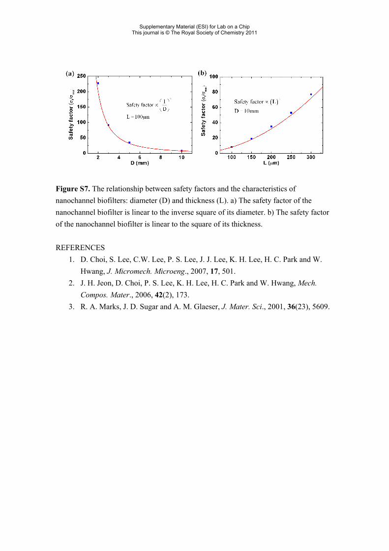
Figure S7. The relationship between safety factors and the characteristics of nanochannel biofilters: diameter (D) and thickness (L). a) The safety factor of the nanochannel biofilter is linear to the inverse square of its diameter. b) The safety factor of the nanochannel biofilter is linear to the square of its thickness. REFERENCES
1. D. Choi, S. Lee, C.W. Lee, P. S. Lee, J. J. Lee, K. H. Lee, H. C. Park and W. Hwang, J. Micromech. Microeng., 2007, 17, 501.
2. J. H. Jeon, D. Choi, P. S. Lee, K. H. Lee, H. C. Park and W. Hwang, Mech. Compos. Mater., 2006, 42(2), 173.
3. R. A. Marks, J. D. Sugar and A. M. Glaeser, J. Mater. Sci., 2001, 36(23), 5609.
Supplementary Material (ESI) for Lab on a ChipThis journal is © The Royal Society of Chemistry 2011


![DEPARTMENT OF METALLURGICAL AND MATERIALS … · [1] R.Sokkalingam, MP Shankar, Anoop K Unni, K Sivaprasad and Veerappan Muthupandi, “Direct Active Soldering of PEO Coated and Uncoated](https://static.fdocuments.net/doc/165x107/5f4dd183045b64163a49219b/department-of-metallurgical-and-materials-1-rsokkalingam-mp-shankar-anoop-k.jpg)