Supporting Information: Holey Silicon as efficient...
16
Supporting Information: Holey Silicon as efficient thermoelectric material Jinyao Tang 1, 3* , Hung-Ta Wang 1* , Dong Hyun Lee 4 , Melissa Fardy 1 , Ziyang Huo 1 , Thomas P. Russell 4 , Peidong Yang 1, 2, 3† 1 Department of Chemistry, 2 Department of Materials Science and Engineering, University of California, Berkeley, California 94720, USA. 3 Materials Sciences Division, Lawrence Berkeley National Laboratory, Berkeley, California 94720, USA. 4 Department of Polymer Science and Engineering, University of Massachusetts, Amherst, MA 01003, USA. * These authors contributed equally to this work. † To whom correspondence should be addressed. E-mail: [email protected] 1. Holey Silicon fabrication The HS ribbons used for transport measurements are patterned by optical lithography and then released from SOI substrate (Soitec Inc.) by hydrofluoric acid vapor etching. The SOI wafer consists 100 nm device layer (<100>, 14-22 Ω·cm, phosphorus doped) with 200 nm buried oxide layer. Holey structure is fabricated by DRIE through thin chromium mask (~5 nm) converted from NSL or BCP pattern. Figure S1 shows the schematic of detailed fabrication of 350 nm and 140 nm pitch HS ribbons. 350 nm and 140 nm polystyrene spheres (Bangs laboratories, Inc.) are 1:4 diluted with de-ionized water and subjected to 2 min sonication before coating to insure homogeneous sphere suspension. The substrate is cleaned with piranha for 10 mins and rinsed with de-ionized water followed by N 2 blow-dry. Polystyrene spheres are self-assembled into hexagonal monolayer film via a dip coating process at speed ~4 μm/s in a customized dip coater equipped with isolating shield to prevent disturbing from air flow. Throughout the assembly process, line defects and point defects are sometimes observed mostly due to the non-uniformity of sphere size. Weak oxygen plasma (20 W at ~300 mtorr in the Technics PEII-A plasma system) is then used to etch polystyrene sphere until the desired spacing is obtained. 5 nm chromium film, served as silicon etching
Transcript of Supporting Information: Holey Silicon as efficient...
Supporting Information:
Holey Silicon as efficient thermoelectric material
Jinyao Tang1, 3*, Hung-Ta Wang1*, Dong Hyun Lee4, Melissa Fardy1, Ziyang Huo1, Thomas P. Russell4,
Peidong Yang1, 2, 3†
1 Department of Chemistry, 2 Department of Materials Science and Engineering, University of California,
Berkeley, California 94720, USA.
3 Materials Sciences Division, Lawrence Berkeley National Laboratory, Berkeley, California 94720, USA.
4 Department of Polymer Science and Engineering, University of Massachusetts, Amherst, MA 01003, USA.
* These authors contributed equally to this work.
† To whom correspondence should be addressed. E-mail: [email protected]
1. Holey Silicon fabrication
The HS ribbons used for transport measurements are patterned by optical lithography
and then released from SOI substrate (Soitec Inc.) by hydrofluoric acid vapor etching. The
SOI wafer consists 100 nm device layer (<100>, 14-22 Ω·cm, phosphorus doped) with 200
nm buried oxide layer. Holey structure is fabricated by DRIE through thin chromium mask
(~5 nm) converted from NSL or BCP pattern. Figure S1 shows the schematic of detailed
fabrication of 350 nm and 140 nm pitch HS ribbons. 350 nm and 140 nm polystyrene spheres
(Bangs laboratories, Inc.) are 1:4 diluted with de-ionized water and subjected to 2 min
sonication before coating to insure homogeneous sphere suspension. The substrate is cleaned
with piranha for 10 mins and rinsed with de-ionized water followed by N2 blow-dry.
Polystyrene spheres are self-assembled into hexagonal monolayer film via a dip coating
process at speed ~4 μm/s in a customized dip coater equipped with isolating shield to prevent
disturbing from air flow. Throughout the assembly process, line defects and point defects are
sometimes observed mostly due to the non-uniformity of sphere size. Weak oxygen plasma
(20 W at ~300 mtorr in the Technics PEII-A plasma system) is then used to etch polystyrene
sphere until the desired spacing is obtained. 5 nm chromium film, served as silicon etching
mask, is deposited with an e-beam evaporator at 2x10⁻⁶ torr, and the polystyrene spheres are
then removed by ultra-sonication in acetone for 5 mins. Silicon etch is performed in a DRIE
system, with 600 W (13.56 MHz) applied on coil and 30 W (380 kHz) on substrate. After 6
cycles of 5 second passivation plus 6 second etching, 100nm silicon layer is completely
etched through. The chromium mask is then removed by soaking the sample in chromium
etchant (CR-7s, from Cyantek) for 2 mins at room temperature.
A similar chromium mask conversion method is applied to BCP lithography for
fabrication of 55 nm pitch HS ribbons, as shown in Figure S2. 55nm-pitch hexagonal
structure is patterned on SOI substrate as stated in SI 2. The 5nm chromium mask is
deposited onto this holey structured BCP film by e-beam evaporation at 60 degree titling
angle. To insure better etching uniformity, sample is further treated with oxygen plasma to
thoroughly remove BCP template in order to ensure the silicon is freshly exposed and can be
etched away by following DRIE process. SEM is then used to carefully examine the holey
structure and >95% etching uniformity of HS is specifically selected for the transport
characterizations.
2. Block copolymer (BCP) assembly and characterization
Polystyrene-block-poly(4-vinylpyridine) (S4VP) copolymer was purchased from
Polymer Source Inc., and used without further purification in this study. Polystyrene
homopolymer was synthesized by anionic polymerization. The number average molecular
weights (Mn) of polystyrene and poly(4-vinylpyridine) were 51 kg/mol and 18 kg/mol,
respectively, and the polydispersity (Mw/Mn) of this BCP was 1.15. The number average
molecular weight and the polydispersity of polystyrene homopolymer (hPS) were 14.4
kg/mol and 1.03, respectively. The mixture of S4VP and hPS with various mixing ratios was
dissolved in the mixture of toluene and tetrahydrofuran (70/30, v/v). S4VP thin films (~ 25
nm) were prepared by spin-coating at 2200 rpm on SOI substrates. The films were solvent-
annealed in tetrahydrofuran vapor for 3 hours to induce lateral ordering of BCP
microdomains. To generate nanoscopic pores, the surface of S4VP thin films was
reconstructed by immersing the substrate into ethanol.
To prevent merging holes during a following DRIE process, it is necessary to spread
out the separation distance among cylindrical microdomains of P4VP. As introducing
hPS(14k) into S4VP(69k) thin film, the pitch of cylindrical microdomians of P4VP was
gradually increased because hPS existed selectively in PS matrix of S4VP thin film. As
shown in Figure S3, the pitch in neat S4VP thin film is about 36.1 nm. By adding hPS(14k),
consequently, it is observed that the pitch of S4VP/hPS (60/40, wt/wt) was finally increased
to 55 nm. In this study, we selected this 55 nm pitch S4VP thin film (Figure S3F) to fabricate
HS.
3. Thermal conductivity measurement and thermal contact resistance calibration
In order to measure HS ribbon’s thermal conductivity, the fabricated ribbons on SOI
chips are released by vapor HF treatment for about 30 seconds, and individual ribbon is then
picked and placed between two SiNx thermal pads by micromanipulation using sharp
tungsten probe tips (GGB Industries) mounted on a scanning stage (Marzhauser SM 3.25).
Then the device is mounted on mask aligner (Karl Suss MA6) and precisely aligned with
prefabricated SiNx stencil mask S1. The stencil mask and thermal device are bonded with I-
line photoresist (OCG OiR 897-10i). After hotplate baking at 95°C for 10 mins, the whole
device/stencil chip is transferred into e-beam evaporator for 300 nm nickel deposition under
2x10⁻⁶ torr. The stencil mask is consequently removed from the device simply by mechanical
force without any damages to the suspended structure or bonded ribbon. Thermal
measurement is conducted with previously reported techniqueS2.
The thermal contact resistance of the nickel bonding is estimated by comparing
thermal resistance of 100nm thick non-holey silicon ribbon covalently fused to SiNx
membrane during the thermal device fabrication process (Figure S4A) with the one of nickel
bonding device (Figure S4B). Since the covalent bonding should mostly show thermal
boundary resistanceS3 which is on the order of 1x10⁻⁴ K/μW in this system, it is negligible in
the measurement as compared to the silicon ribbon’s thermal resistance around 5 K/μW. In
order to calibrate the thermal contact resistance of Ni bonding, a 30 μm long, 1 μm wide non-
HS ribbon is bonded to thermal device with same protocol as described previously. The
measured data is then compared with covalently bonding device with same ribbon geometry.
As shown in Figure S4C, the contact resistance of nickel bonding is obtained as the total
resistance difference of the two devices, and is around 1.5 K/μW at room temperature. This
contact resistance is around 10% of total resistance for 350nm pitch HS, ~6% for 140 nm
pitch HS, and ~3% for 55nm pitch HS, specifically shown in Figure S4D.
4. Thermal conductivity of HS and comparison with theory
To verify the reproducibility of low thermal conductivity in 55nm pitch HS, multiple
samples are prepared among several batches. Representative temperature dependent thermal
measurement datas are shown in Figure S5. Room temperature thermal conductivities with
ribbon geometry are summarized in Table S1. Consistent low thermal conductivities, ranging
from 1.14 to 2.03 W/m·K are routinely recorded. The thermal conductivity variation observed
is mainly due to the small porosity difference from sample to sample.
Considering a uniform hexagonal lattice of holes of pitch (center-to-center distance),
p and radius, r, simple geometry shows that the porosity φ is,
2
2
63p
rπϕ =
For 35% porosity HS, specifically for 55nm, 140nm, and 350nm HS, this “bottleneck”,
n is 23nm, 59nm, and 152nm, respectively. As discussed in the main text, the necking effect
should be responsible for the low thermal conductivity of HS. Two parameters affect the
necking effect: pitch and neck. Lower thermal conductivity is expected when the pitch size
gets smaller than the frequency dependent phonon MFP; and when the necking becomes
smaller, κ can be further suppressed. The first parameter, pitch size, is discussed in main text
and shown in Figure 2d. To verify the neck effect, we prepared 350nm HS with different
porosity by varying polystyrene size using different oxygen plasma etching time (from 30s to
3mins with 50W); 13%, 27%, 35%, and 40% HS are prepared with the same approach
described in section 1. Due to the imperfection of holes packing, the actually necking width is
smaller than the ideal values calculated from the perfect hexagonal array of holes, which are
around 160nm, 110nm, 70nm and 40nm respectively. In Figure S6, the room temperature
thermal conductivities show a clear decrease by shrinking the neck width (increasing
porosity), and thus confirmed that the necking effect does play the important role in reducing
the HS thermal conductivity.
A quantitative comparison between the literature data (including model S4, S5 and
experiment S6) to the present experiments has been summarized in Figure S6. All our thermal
conductivity data are normalized by its porosity. We specifically compared to Hao et al’s
model because the dimension is the closest to our system. The simulation is 2D which would
represent perfect bulk lattice in z direction, while in our system the phonon scattering on top
and bottom surface should be considered. As in non-holey silicon, this top/bottom surface

scattering lowers the thermal conductivity from 150 W/m·K in bulk to ~50 W/m·K in 100nm
thin film. We estimated 66% reduction in thermal conductivity to correct the thickness
discrepancy. The corrected value (i.e. bulk of 25% porosity corrected by the dimension effect)
is around 19.3 W/m·K which is quite close to our measurement value 14.5 W/m·K for 27%
porosity 350nm pitch HS. Moreover, the porosity different from 27% to 35% will cause
another 33% thermal conductivity reduction according to our measurement. In total, we
roughly obtain a correction factor ~0.22. We further apply this correction factor to evaluate
the 55nm pitch which result 4-5 W/m·K, and this value is still higher than our measurement
data. However, the discrepancy is not significant especially there are additional parameters
could play a role, such as hole sidewall roughness created in DRIE.
5. Electrical measurement
The electrical conductivity is measured by the four point electrical device as shown in
Figure S7. The ribbons are usually 1-2 μm in width and 20-40 μm in length. Most uncertainty
of ρ measurement is coming from the ribbon width measurement which can vary up to 4.7%
within the measured length. Since the uncertainty from electrical measurement noise is less
than 0.1%, we define that the uncertainty of ρ measurement is 4.7%.
For the thermopower measurement, the inner two Pt electrodes are connected to
Keithley 2182A nanovoltmeter for Seebeck voltage measurement while DC current is applied
to heating coil by Keithley 236 source measurement unit to generate temperature gradient.
The local temperature is measured by four probe resistance of the inner Pt electrode. As
described in previous study, the error of this measurement is estimated as less than 3% due to
possible systematic errors of this method S7.
Supplementary information references S1. Vazquez-Mena, O.; Villanueva, G.; Savu, V.; Sidler, K.; van den Boogaart, M. A. F.; Brugger, J. Nano Lett 2008, 8, (11), 3675-82. S2. Shi, L.; Li, D.; Yu, C.; Jang, W.; Kim, D.; Yao, Z.; Kim, P.; Majumdar, A. J. Heat Transfer 2003, 125, (5), 881-888. S3. Swartz, E. T.; Pohl, R. O. Reviews of Modern Physics 1989, 61, (3), 605. S4. Lee, J.-H.; Galli, G. A.; Grossman, J. C. Nano Lett. 2008, 8, (11), 3750-3754. S5. Hao, Q.; Chen, G.; Jeng, M.-S. J. Appl. Phys. 2009, 106, (11), 114321/1-114321/10. S6. Song, D.; Chen, G. Appl. Phys. Lett. 2004, 84, (5), 687-689. S7. Hochbaum, A. I.; Chen, R.; Delgado, R. D.; Liang, W.; Garnett, E. C.; Najarian, M.; Majumdar, A.; Yang, P. Nature (London, U. K.) 2008, 451, (7175), 163-167.

Supplementary information figures Figure S1
Figure S1. Illustration of HS fabrication based on nanosphere lithography.
(A) Polystyrene spheres are assembled in monolayer on SOI substrate. (B) Nanospheres are
etched with mild oxygen plasma to obtain the desired separation. (C) 5 nm chromium film is
deposited followed by sphere lift-off in acetone to form holey structured chromium mask. (D)
DRIE etched HS through mask and Cr mask is finally removed.
A B
C D
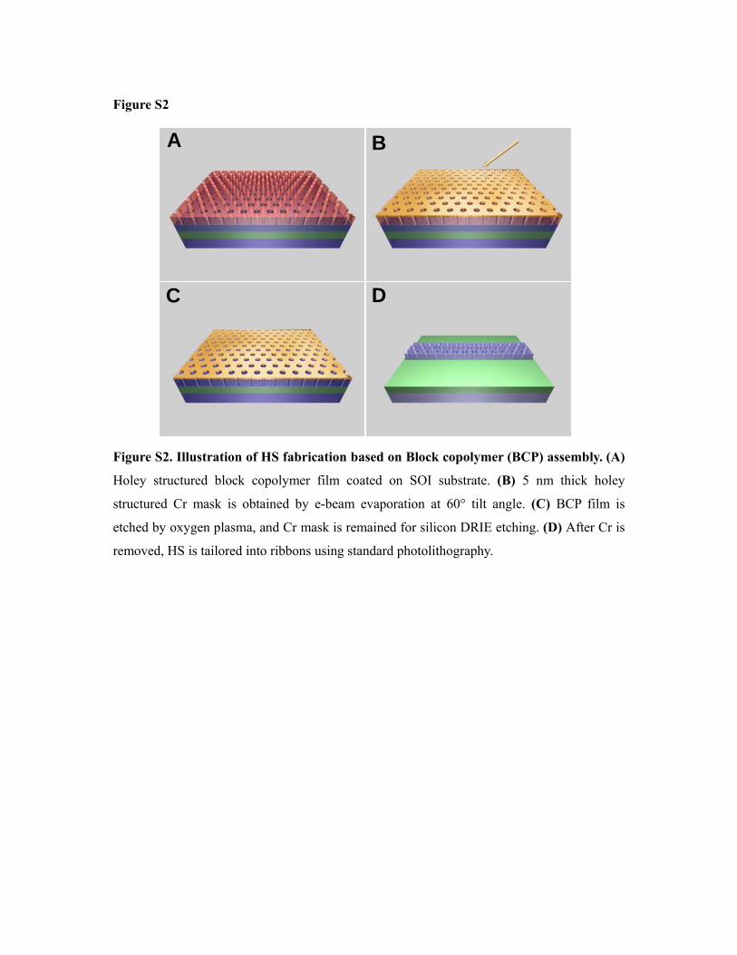
Figure S2
Figure S2. Illustration of HS fabrication based on Block copolymer (BCP) assembly. (A)
Holey structured block copolymer film coated on SOI substrate. (B) 5 nm thick holey
structured Cr mask is obtained by e-beam evaporation at 60° tilt angle. (C) BCP film is
etched by oxygen plasma, and Cr mask is remained for silicon DRIE etching. (D) After Cr is
removed, HS is tailored into ribbons using standard photolithography.
A B
C D
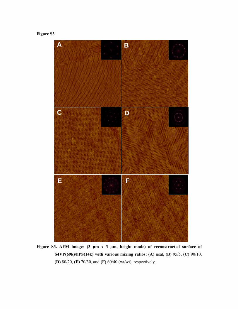
Figure S3
Figure S3. AFM images (3 μm x 3 μm, height mode) of reconstructed surface of
S4VP(69k)/hPS(14k) with various mixing ratios: (A) neat, (B) 95/5, (C) 90/10,
(D) 80/20, (E) 70/30, and (F) 60/40 (wt/wt), respectively.
A B
C D
E F
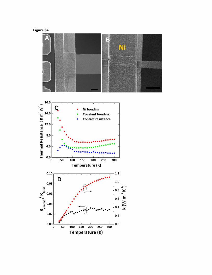
Figure S4
A
B
B Ni
D
C
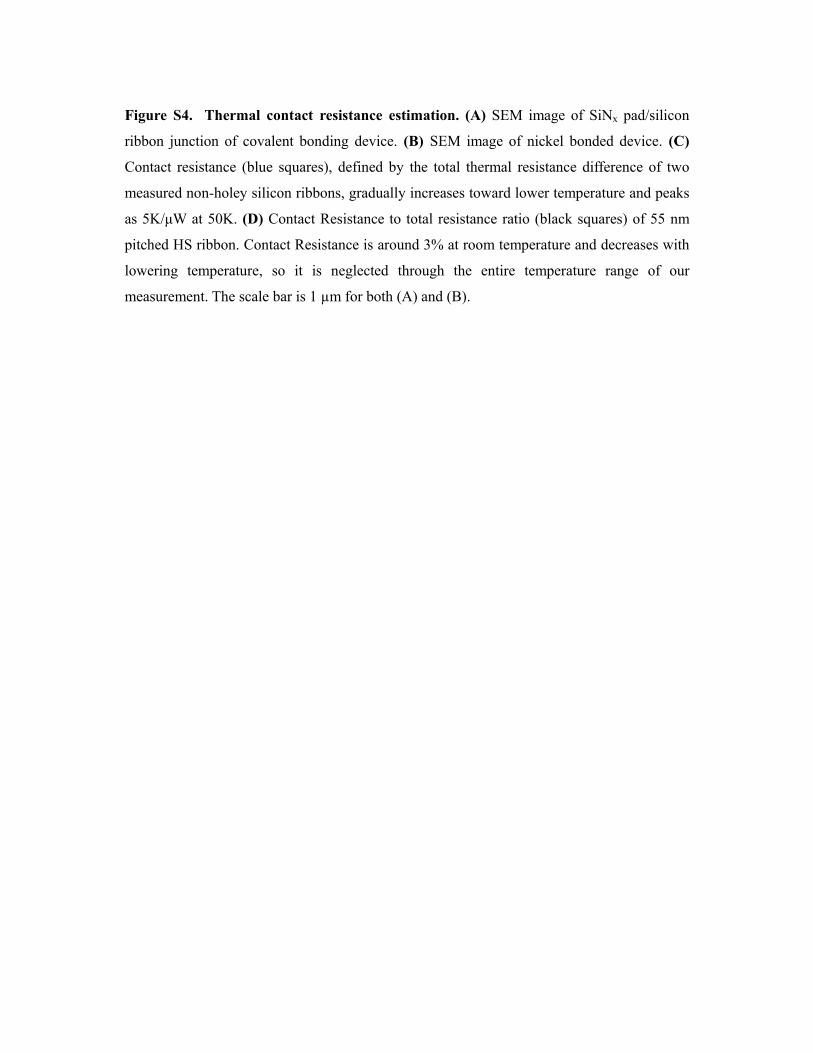
Figure S4. Thermal contact resistance estimation. (A) SEM image of SiNx pad/silicon
ribbon junction of covalent bonding device. (B) SEM image of nickel bonded device. (C)
Contact resistance (blue squares), defined by the total thermal resistance difference of two
measured non-holey silicon ribbons, gradually increases toward lower temperature and peaks
as 5K/μW at 50K. (D) Contact Resistance to total resistance ratio (black squares) of 55 nm
pitched HS ribbon. Contact Resistance is around 3% at room temperature and decreases with
lowering temperature, so it is neglected through the entire temperature range of our
measurement. The scale bar is 1 µm for both (A) and (B).
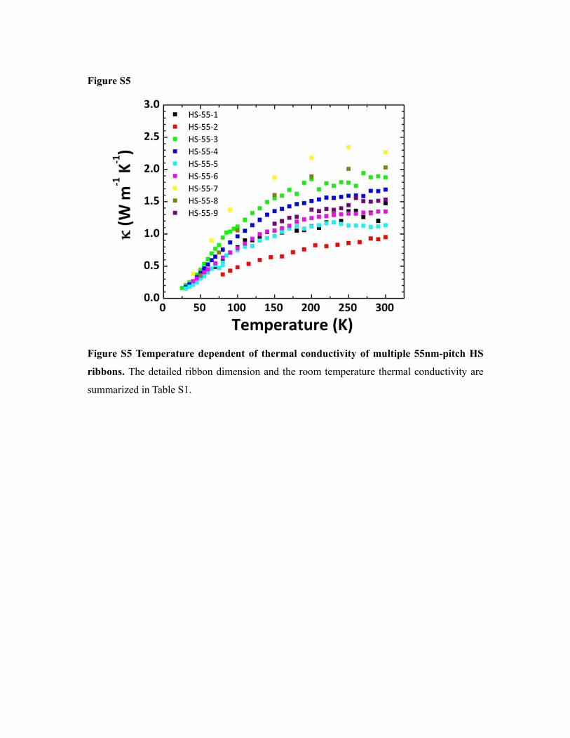
Figure S5
Figure S5 Temperature dependent of thermal conductivity of multiple 55nm-pitch HS
ribbons. The detailed ribbon dimension and the room temperature thermal conductivity are
summarized in Table S1.
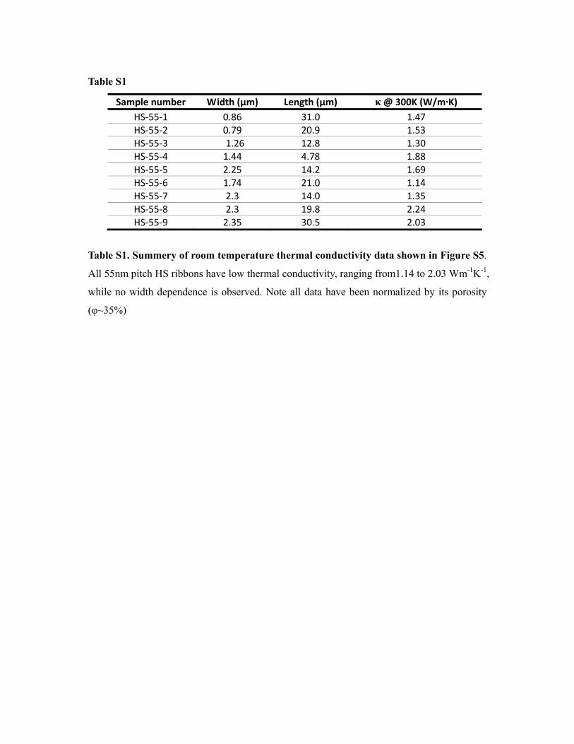
Table S1
Sample number Width (μm) Length (μm) κ @ 300K (W/m·K) HS‐55‐1 0.86 31.0 1.47 HS‐55‐2 0.79 20.9 1.53 HS‐55‐3 1.26 12.8 1.30 HS‐55‐4 1.44 4.78 1.88 HS‐55‐5 2.25 14.2 1.69 HS‐55‐6 1.74 21.0 1.14 HS‐55‐7 2.3 14.0 1.35 HS‐55‐8 2.3 19.8 2.24 HS‐55‐9 2.35 30.5 2.03
Table S1. Summery of room temperature thermal conductivity data shown in Figure S5.
All 55nm pitch HS ribbons have low thermal conductivity, ranging from1.14 to 2.03 Wm-1K-1,
while no width dependence is observed. Note all data have been normalized by its porosity
(φ~35%)
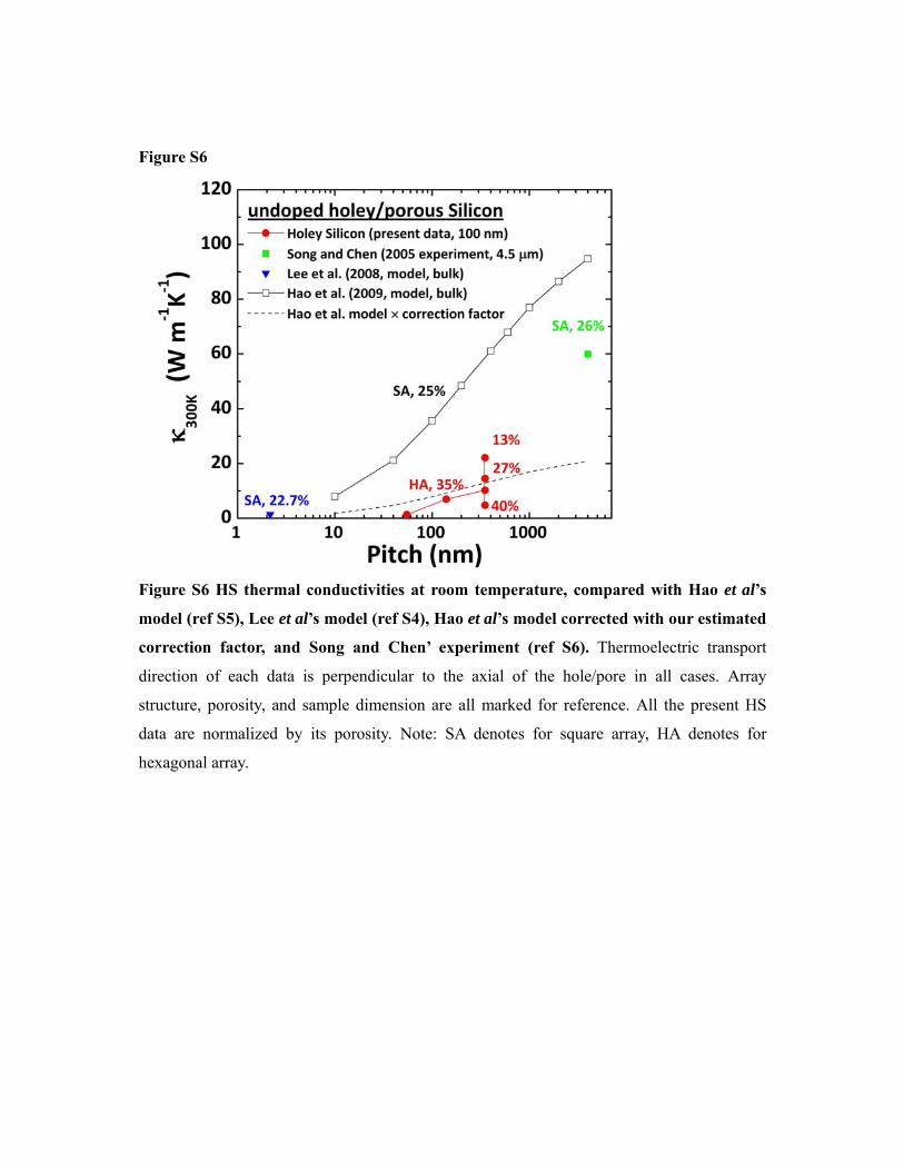
Figure S6
Figure S6 HS thermal conductivities at room temperature, compared with Hao et al’s
model (ref S5), Lee et al’s model (ref S4), Hao et al’s model corrected with our estimated
correction factor, and Song and Chen’ experiment (ref S6). Thermoelectric transport
direction of each data is perpendicular to the axial of the hole/pore in all cases. Array
structure, porosity, and sample dimension are all marked for reference. All the present HS
data are normalized by its porosity. Note: SA denotes for square array, HA denotes for
hexagonal array.
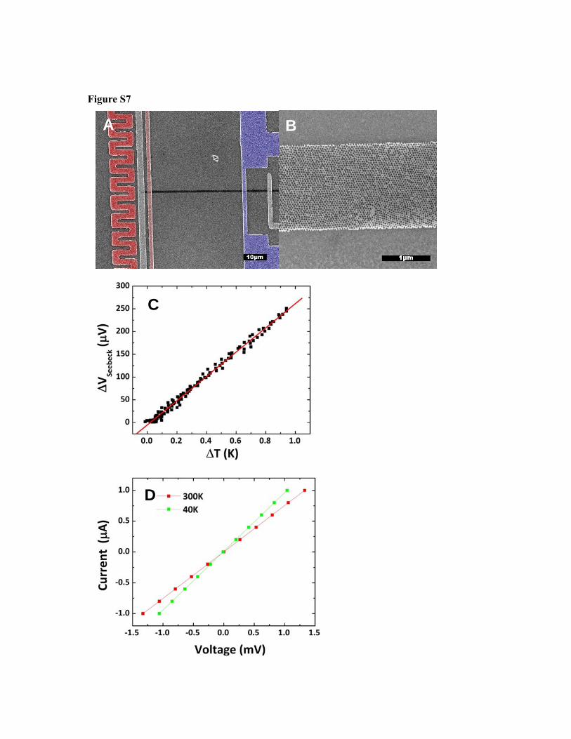
Figure S7
BA
C
D
Figure S7. HS ribbon thermopower and electrical conductivity measurement
(A) SEM image of a typical device used for electrical measurement. The left heating coil is
used to create uniform temperature gradient. Two inner Pt electrodes are used for seebeck
voltage measurement and temperature sensing, while all four electrdes are used for four probe
ρ measurement. (B) SEM image of high magnification of HS ribbon for electrical
measurement (C) Typical plot of seebeck volatage vs temperature difference. (D) I-V plot by
four probe electrical resistance measurement. (C) and (D) plots are for the 55 nm pitch ribbon
shown in Figure 3a.