Superconducting metamaterials and qubits - Syracuse...
7
Superconducting metamaterials and qubits B.L.T. Plourde a , Haozhi Wang a , Francisco Rouxinol a , M.D. LaHaye a a Department of Physics, Syracuse University, Syracuse, NY 13244-1130, USA ABSTRACT Superconducting thin-film metamaterial resonators can provide a dense microwave mode spectrum with potential applications in quantum information science. We report on the fabrication and low-temperature measurement of metamaterial transmission-line resonators patterned from Al thin films. We also describe multiple approaches for numerical simulations of the microwave properties of these structures, along with comparisons with the measured transmission spectra. The ability to predict the mode spectrum based on the chip layout provides a path towards future designs integrating metamaterial resonators with superconducting qubits. Keywords: Superconducting devices, metamaterials, microwave circuits, qubits 1. INTRODUCTION Metamaterials having both a negative permeability and permittivity, and thus a negative index of refraction with left-handed transmission properties, were first described several decades ago. 1 More recently there have been numerous investigations of a variety of counterintuitive optical properties in these systems, including cloaking 2 and superlensing. 3 Research in this direction is closely connected to the field of photonic band-gap engineering. 4 In the microwave regime, left-handed transmission lines have been proposed and studied with one- and two- dimensional arrays of room-temperature lumped-element components. 5, 6 There have also been implementations of one-dimensional metamaterial microwave transmission lines with high-temperature superconducting films. 7 Since 1999, there has been substantial progress in the field of quantum coherent superconducting circuits, or qubits. 8 Many superconducting qubit implementations involve couplings between the qubits and superconducting microwave resonator circuits. In this architecture, referred to as circuit quantum electrodynamics, or cQED, 9–11 the qubit behaves as an artificial atom that can couple to photons in the microwave resonant cavity, analogous to atomic QED with natural atoms in microwave or optical cavities. 12 In cQED, the microwave resonators are typically either distributed coplanar waveguide cavities patterned from superconducting thin films 13 or three- dimensional waveguide cavities. 14, 15 A recent theoretical work suggested the possibility of implementing one-dimensional superconducting meta- material resonators in the microwave regime with high quality factors for coupling to superconducting qubits. 16 Such a system could allow for the generation of large-scale entanglement between multiple photon modes in the metamaterial and could have potential applications in the emerging field of quantum simulation. Here we report on the fabrication of thin-film superconducting metamaterial resonators and test oscillators along with microwave measurements at millikelvin temperatures. We also present numerical simulations of the metamaterial circuits and compare the simulated and measured spectra. The metamaterial architectures that we present here are compatible with future circuit designs for exploring the coupling to superconducting qubits. Further author information: (Send correspondence to B.L.T.P.) B.L.T.P.: E-mail: [email protected]
Transcript of Superconducting metamaterials and qubits - Syracuse...
Superconducting metamaterials and qubits
B.L.T. Plourdea, Haozhi Wanga, Francisco Rouxinola, M.D. LaHayea
aDepartment of Physics, Syracuse University, Syracuse, NY 13244-1130, USA
ABSTRACT
Superconducting thin-film metamaterial resonators can provide a dense microwave mode spectrum with potentialapplications in quantum information science. We report on the fabrication and low-temperature measurement ofmetamaterial transmission-line resonators patterned from Al thin films. We also describe multiple approaches fornumerical simulations of the microwave properties of these structures, along with comparisons with the measuredtransmission spectra. The ability to predict the mode spectrum based on the chip layout provides a path towardsfuture designs integrating metamaterial resonators with superconducting qubits.
Keywords: Superconducting devices, metamaterials, microwave circuits, qubits
1. INTRODUCTION
Metamaterials having both a negative permeability and permittivity, and thus a negative index of refraction withleft-handed transmission properties, were first described several decades ago.1 More recently there have beennumerous investigations of a variety of counterintuitive optical properties in these systems, including cloaking2
and superlensing.3 Research in this direction is closely connected to the field of photonic band-gap engineering.4
In the microwave regime, left-handed transmission lines have been proposed and studied with one- and two-dimensional arrays of room-temperature lumped-element components.5,6 There have also been implementationsof one-dimensional metamaterial microwave transmission lines with high-temperature superconducting films.7
Since 1999, there has been substantial progress in the field of quantum coherent superconducting circuits, orqubits.8 Many superconducting qubit implementations involve couplings between the qubits and superconductingmicrowave resonator circuits. In this architecture, referred to as circuit quantum electrodynamics, or cQED,9–11
the qubit behaves as an artificial atom that can couple to photons in the microwave resonant cavity, analogousto atomic QED with natural atoms in microwave or optical cavities.12 In cQED, the microwave resonators aretypically either distributed coplanar waveguide cavities patterned from superconducting thin films13 or three-dimensional waveguide cavities.14,15
A recent theoretical work suggested the possibility of implementing one-dimensional superconducting meta-material resonators in the microwave regime with high quality factors for coupling to superconducting qubits.16
Such a system could allow for the generation of large-scale entanglement between multiple photon modes in themetamaterial and could have potential applications in the emerging field of quantum simulation.
Here we report on the fabrication of thin-film superconducting metamaterial resonators and test oscillatorsalong with microwave measurements at millikelvin temperatures. We also present numerical simulations of themetamaterial circuits and compare the simulated and measured spectra. The metamaterial architectures thatwe present here are compatible with future circuit designs for exploring the coupling to superconducting qubits.
Further author information: (Send correspondence to B.L.T.P.)B.L.T.P.: E-mail: [email protected]
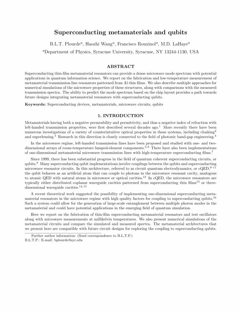
Figure 1. Circuit schematics for (a) right-handed and (b) left-handed lumped-element lines. S21 spectra simulated inAWR Microwave Office for (c) right-handed and (d) left-handed transmission-line resonators.
2. DESIGN AND FABRICATION
2.1 Metamaterials with microwave circuit components
Although typical planar cQED implementations involve distributed coplanar waveguide (CPW) resonators fab-ricated from superconducting thin films on silicon or sapphire substrates,13 a resonator could also be formedfrom a lumped-element transmission line, consisting of a one-dimensional chain of unit cells each with a seriesinductor Ll and a capacitor Cl to ground [Fig. 1(a)].17 Such a resonant circuit would exhibit a fundamental res-onance at f0 = 1/2N
√LlCl, where N is the number of unit cells between the input/output coupling capacitors.
Beyond the fundamental resonance, there are evenly spaced harmonics at integer multiples of f0, as shown in acircuit simulation performed in AWR Microwave Office [Fig. 1(c)]. The dispersion relation for such a circuit isan increasing function of the wavenumber, characteristic of right-handed transmission.
As described in Refs [5, 16],5,16 by interchanging the positions of the capacitors and inductors in the lumped-element right-handed transmission line resonator described above [Fig. 1(b)], one obtains a circuit with dramati-cally different transmission properties. There is now a low-frequency infrared cut-off at fIR = 1/4π
√LlCl, below
which there is no transmission through the structure. For frequencies just above fIR, there is a dense forest ofresonances that get further apart for higher frequencies. The density of resonances for f > fIR increases as moreunit cells are added to the transmission line. As with a conventional right-handed lumped-element transmissionline, the impedance is still given by Z0 =
√Ll/Cl.
2.2 Metamaterial design and fabrication
We design our metamaterial resonators with a target range of fIR ∼ 5 GHz in order to place the densestportion of the metamaterial spectrum in the range of tunability for a typical superconducting transmon qubit.18
The use of an asymmetric transmon with two different sizes of junctions19 would allow the IR cut-off for themetamaterial resonator to be located between the upper and lower high-coherence flux-insensitive sweetspots.Our target impedance for the metamaterial lines is Z0 = 50 Ω, which, when combined with fIR = 5 GHz, resultsin Cl = 300 fF and Ll = 0.8 nH.
We fabricate our metamaterial structures on a Si wafer with conventional photolithographic patterning usinga DUV stepper followed by a lift-off process with electron-beam deposition of Al thin films, a common materialin superconducting qubit circuits. The Al films are 90 nm thick. For our initial metamaterial structures we haveused interdigitated capacitors, which allow for a straightforward single-layer fabrication process, although thecapacitors occupy a relatively large area and their physical size limits the number of unit cells that we are ableto fit on a chip. Our present capacitor design has fingers that are 4µm wide, with a separation of 1µm betweenadjacent fingers and an overlap length of 50µm [Fig. 2(a, c)]. For the inductors, we use a meander-line design

Figure 2. Optical micrographs of type-A superconducting metamaterial transmission-line resonator: (a) close-up of first5 unit cells, (b) coupling capacitor at one end of metamaterial, (c) close-up of interdigitated fingers in capacitor, (d)zoomed-out image of entire chip, (e) close-up image of two inductors.
with a linewidth of 2µm, gaps between adjacent lines of 3µm, with a length for each turn of the meander lineof 60µm [Fig. 2(e)].
In order to explore the impact of the lumped-element parameter values on the resonance spectrum, we havefabricated two different versions of metamaterial resonators: type A and type B. In both cases, we have attemptedto maintain the ratio of Ll and Cl for Z0 ∼ 50 Ω while varying their product to change fIR. On the type A (B)structures, each capacitor has 32 (26) pairs of fingers and each inductor has 12 (7) turns of the meander line.
We have chosen the lumped-element parameters based on a variety of techniques for estimating the resultingcapacitance and inductance values. For the capacitors, numerical simulations based on ANSYS Q3D yield acapacitance per finger pair of 8.35 fF, corresponding to CA
l = 267 fF and CBl = 217 fF. For the inductors, from
an analysis with Sonnet, we obtain inductance estimates LAl = 0.9 nH and LB
l = 0.6 nH. We note that theseestimates do not account for kinetic inductance. However, for our relatively wide traces on the inductors and theshort penetration depth of Al, we estimate the kinetic inductance contribution to be less than 5% of the totalinductance for each Ll.
Both metamaterial structures consist of 42 unit cells extending across the width of a 6 mm-wide chip [Fig. 2(d)]with gap coupling capacitors at either end of the metamaterial [Fig. 2(b)]. For the type A(B) metamaterialresonators, the gap capacitor is 1 (5)µm wide, in order to target a coupling capacitance of 50 (28) fF. Eachchip has an Al ground plane surrounding the metamaterial structure and CPW leads for probing the microwavetransmission. As is typically done in many cQED implementations, the ground plane contains a lattice of holesto avoid the trapping of Abrikosov vortices in regions of large microwave currents that could contribute excessloss.20
3. DEVICE MEASUREMENTS
3.1 Measurements of test oscillators
Before measuring the metamaterial resonators, we have designed and tested a series of lumped-element testoscillators fabricated with the same process and lumped-element parameters as in the metamaterials. The testoscillator chips each consist of four lumped-element LC oscillators, each one capacitively coupled to a CPWfeedline. Each test oscillator has the same inductor as in a unit cell of metamaterial A or B and the capacitorhas the same interdigitated finger parameters as in the corresponding metamaterial line, although the capacitoris split in two halves that are arranged in parallel on either side of the inductor. The total number of fingerpairs in the capacitor for oscillator number 1-4 is 29, 33, 37, or 41, respectively, thus allowing us to study thevariation in capacitance for different numbers of fingers [Fig. 3(a, b)].
We perform our measurements of the test oscillators on an adiabatic demagnetization refrigerator (ADR) ata temperature of ∼ 50 mK. We probe the microwave transmission S21 through the feedline with a vector network
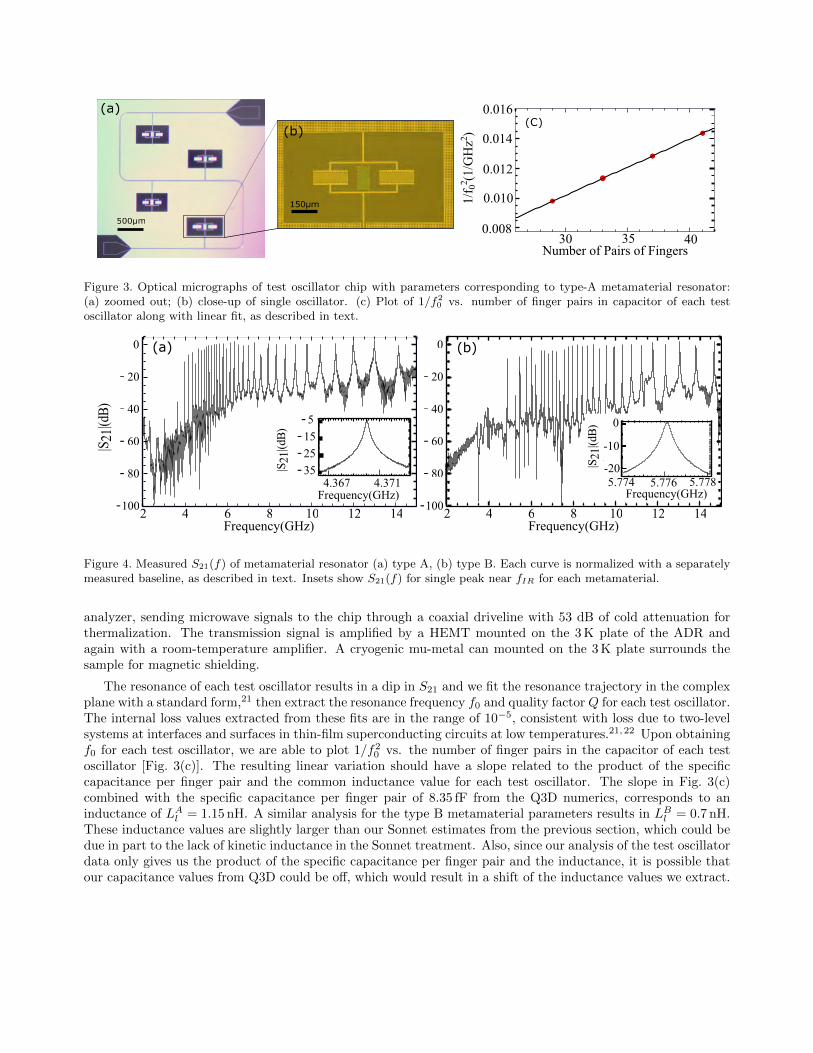
Figure 3. Optical micrographs of test oscillator chip with parameters corresponding to type-A metamaterial resonator:(a) zoomed out; (b) close-up of single oscillator. (c) Plot of 1/f2
0 vs. number of finger pairs in capacitor of each testoscillator along with linear fit, as described in text.
Figure 4. Measured S21(f) of metamaterial resonator (a) type A, (b) type B. Each curve is normalized with a separatelymeasured baseline, as described in text. Insets show S21(f) for single peak near fIR for each metamaterial.
analyzer, sending microwave signals to the chip through a coaxial driveline with 53 dB of cold attenuation forthermalization. The transmission signal is amplified by a HEMT mounted on the 3 K plate of the ADR andagain with a room-temperature amplifier. A cryogenic mu-metal can mounted on the 3 K plate surrounds thesample for magnetic shielding.
The resonance of each test oscillator results in a dip in S21 and we fit the resonance trajectory in the complexplane with a standard form,21 then extract the resonance frequency f0 and quality factor Q for each test oscillator.The internal loss values extracted from these fits are in the range of 10−5, consistent with loss due to two-levelsystems at interfaces and surfaces in thin-film superconducting circuits at low temperatures.21,22 Upon obtainingf0 for each test oscillator, we are able to plot 1/f20 vs. the number of finger pairs in the capacitor of each testoscillator [Fig. 3(c)]. The resulting linear variation should have a slope related to the product of the specificcapacitance per finger pair and the common inductance value for each test oscillator. The slope in Fig. 3(c)combined with the specific capacitance per finger pair of 8.35 fF from the Q3D numerics, corresponds to aninductance of LA
l = 1.15 nH. A similar analysis for the type B metamaterial parameters results in LBl = 0.7 nH.
These inductance values are slightly larger than our Sonnet estimates from the previous section, which could bedue in part to the lack of kinetic inductance in the Sonnet treatment. Also, since our analysis of the test oscillatordata only gives us the product of the specific capacitance per finger pair and the inductance, it is possible thatour capacitance values from Q3D could be off, which would result in a shift of the inductance values we extract.
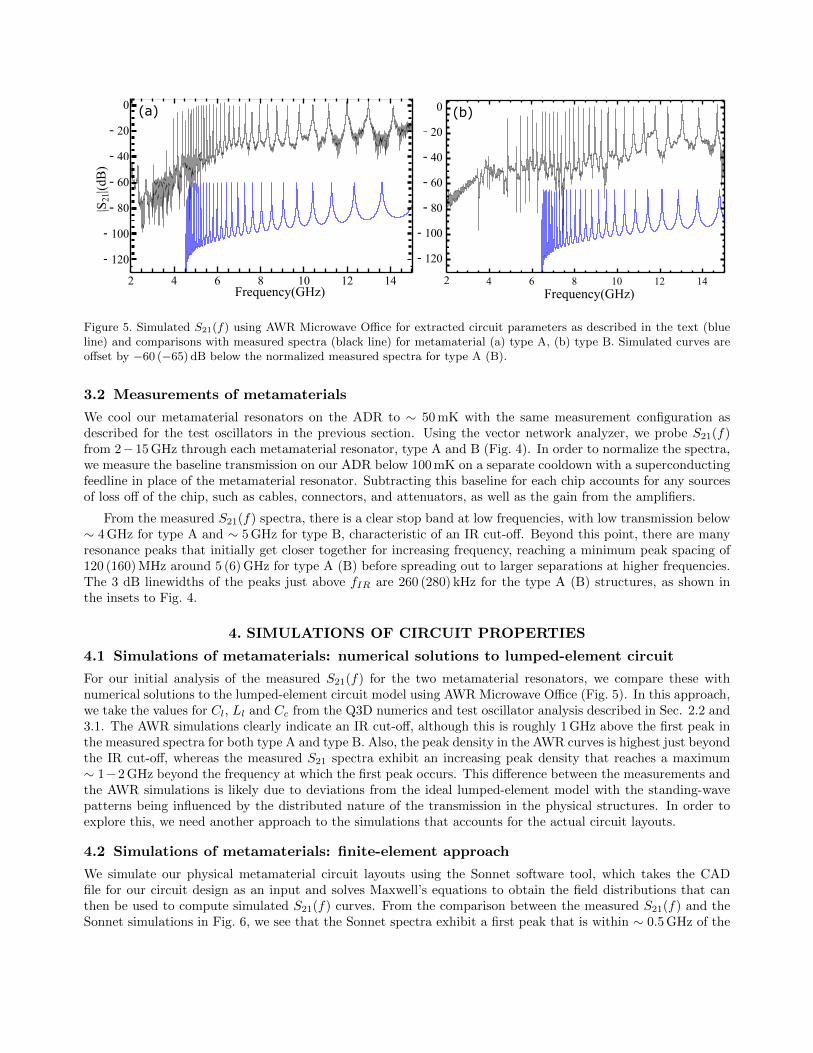
Figure 5. Simulated S21(f) using AWR Microwave Office for extracted circuit parameters as described in the text (blueline) and comparisons with measured spectra (black line) for metamaterial (a) type A, (b) type B. Simulated curves areoffset by −60 (−65) dB below the normalized measured spectra for type A (B).
3.2 Measurements of metamaterials
We cool our metamaterial resonators on the ADR to ∼ 50 mK with the same measurement configuration asdescribed for the test oscillators in the previous section. Using the vector network analyzer, we probe S21(f)from 2−15 GHz through each metamaterial resonator, type A and B (Fig. 4). In order to normalize the spectra,we measure the baseline transmission on our ADR below 100 mK on a separate cooldown with a superconductingfeedline in place of the metamaterial resonator. Subtracting this baseline for each chip accounts for any sourcesof loss off of the chip, such as cables, connectors, and attenuators, as well as the gain from the amplifiers.
From the measured S21(f) spectra, there is a clear stop band at low frequencies, with low transmission below∼ 4 GHz for type A and ∼ 5 GHz for type B, characteristic of an IR cut-off. Beyond this point, there are manyresonance peaks that initially get closer together for increasing frequency, reaching a minimum peak spacing of120 (160) MHz around 5 (6) GHz for type A (B) before spreading out to larger separations at higher frequencies.The 3 dB linewidths of the peaks just above fIR are 260 (280) kHz for the type A (B) structures, as shown inthe insets to Fig. 4.
4. SIMULATIONS OF CIRCUIT PROPERTIES
4.1 Simulations of metamaterials: numerical solutions to lumped-element circuit
For our initial analysis of the measured S21(f) for the two metamaterial resonators, we compare these withnumerical solutions to the lumped-element circuit model using AWR Microwave Office (Fig. 5). In this approach,we take the values for Cl, Ll and Cc from the Q3D numerics and test oscillator analysis described in Sec. 2.2 and3.1. The AWR simulations clearly indicate an IR cut-off, although this is roughly 1 GHz above the first peak inthe measured spectra for both type A and type B. Also, the peak density in the AWR curves is highest just beyondthe IR cut-off, whereas the measured S21 spectra exhibit an increasing peak density that reaches a maximum∼ 1−2 GHz beyond the frequency at which the first peak occurs. This difference between the measurements andthe AWR simulations is likely due to deviations from the ideal lumped-element model with the standing-wavepatterns being influenced by the distributed nature of the transmission in the physical structures. In order toexplore this, we need another approach to the simulations that accounts for the actual circuit layouts.
4.2 Simulations of metamaterials: finite-element approach
We simulate our physical metamaterial circuit layouts using the Sonnet software tool, which takes the CADfile for our circuit design as an input and solves Maxwell’s equations to obtain the field distributions that canthen be used to compute simulated S21(f) curves. From the comparison between the measured S21(f) and theSonnet simulations in Fig. 6, we see that the Sonnet spectra exhibit a first peak that is within ∼ 0.5 GHz of the
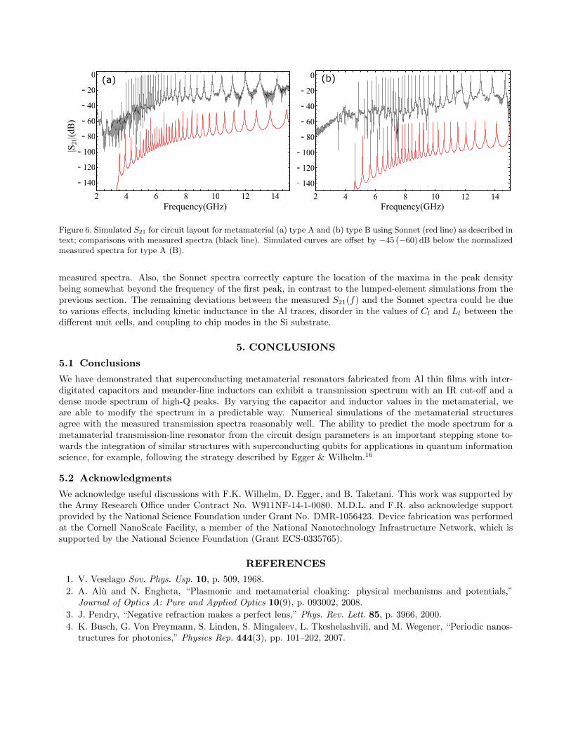
Figure 6. Simulated S21 for circuit layout for metamaterial (a) type A and (b) type B using Sonnet (red line) as described intext; comparisons with measured spectra (black line). Simulated curves are offset by −45 (−60) dB below the normalizedmeasured spectra for type A (B).
measured spectra. Also, the Sonnet spectra correctly capture the location of the maxima in the peak densitybeing somewhat beyond the frequency of the first peak, in contrast to the lumped-element simulations from theprevious section. The remaining deviations between the measured S21(f) and the Sonnet spectra could be dueto various effects, including kinetic inductance in the Al traces, disorder in the values of Cl and Ll between thedifferent unit cells, and coupling to chip modes in the Si substrate.
5. CONCLUSIONS
5.1 Conclusions
We have demonstrated that superconducting metamaterial resonators fabricated from Al thin films with inter-digitated capacitors and meander-line inductors can exhibit a transmission spectrum with an IR cut-off and adense mode spectrum of high-Q peaks. By varying the capacitor and inductor values in the metamaterial, weare able to modify the spectrum in a predictable way. Numerical simulations of the metamaterial structuresagree with the measured transmission spectra reasonably well. The ability to predict the mode spectrum for ametamaterial transmission-line resonator from the circuit design parameters is an important stepping stone to-wards the integration of similar structures with superconducting qubits for applications in quantum informationscience, for example, following the strategy described by Egger & Wilhelm.16
5.2 Acknowledgments
We acknowledge useful discussions with F.K. Wilhelm, D. Egger, and B. Taketani. This work was supported bythe Army Research Office under Contract No. W911NF-14-1-0080. M.D.L. and F.R. also acknowledge supportprovided by the National Science Foundation under Grant No. DMR-1056423. Device fabrication was performedat the Cornell NanoScale Facility, a member of the National Nanotechnology Infrastructure Network, which issupported by the National Science Foundation (Grant ECS-0335765).
REFERENCES
1. V. Veselago Sov. Phys. Usp. 10, p. 509, 1968.
2. A. Alu and N. Engheta, “Plasmonic and metamaterial cloaking: physical mechanisms and potentials,”Journal of Optics A: Pure and Applied Optics 10(9), p. 093002, 2008.
3. J. Pendry, “Negative refraction makes a perfect lens,” Phys. Rev. Lett. 85, p. 3966, 2000.
4. K. Busch, G. Von Freymann, S. Linden, S. Mingaleev, L. Tkeshelashvili, and M. Wegener, “Periodic nanos-tructures for photonics,” Physics Rep. 444(3), pp. 101–202, 2007.
5. G. V. Eleftheriades, A. K. Iyer, and P. C. Kremer, “Planar negative refractive index media using periodicallylc loaded transmission lines,” IEEE Trans. Microwave Theory and Tech. 50(12), pp. 2702–2712, 2002.
6. A. K. Iyer and G. V. Eleftheriades, Negative-Refractive-Index Transmission-Line (NRI-TL) MetamaterialLenses and Superlenses. Taylor & Francis-CRC, Boca Raton, 2009.
7. Y. Wang and M. J. Lancaster, “High-temperature superconducting coplanar left-handed transmission linesand resonators,” IEEE Trans. Appl. Supercon. 16(3), pp. 1893–1897, 2006.
8. J. Clarke and F. K. Wilhelm, “Superconducting quantum bits,” Nature 453, p. 1031, 2008.
9. A. Wallraff, D. Schuster, A. Blais, L. Frunzio, R. Huang, J. Majer, S. Kumar, S. Girvin, and R. Schoelkopf,“Strong coupling of a single photon to a superconducting qubit using circuit quantum electrodynamics,”Nature 431(7005), pp. 162–167, 2004.
10. A. Blais, R.-S. Huang, A. Wallraff, S. M. Girvin, and R. J. Schoelkopf, “Cavity quantum electrodynamics forsuperconducting electrical circuits: An architecture for quantum computation,” Phys. Rev. A 69, p. 062320,Jun 2004.
11. R. Schoelkopf and S. Girvin, “Wiring up quantum systems,” Nature 451(7179), pp. 664–670, 2008.
12. J. M. Raimond, M. Brune, and S. Haroche, “Manipulating quantum entanglement with atoms and photonsin a cavity,” Rev. Mod. Phys. 73, pp. 565–582, Aug 2001.
13. M. Goppl, A. Fragner, M. Baur, R. Bianchetti, S. Filipp, J. Fink, P. Leek, G. Puebla, L. Steffen, andA. Wallraff, “Coplanar waveguide resonators for circuit quantum electrodynamics,” Journal of AppliedPhysics 104(11), pp. 113904–113904, 2008.
14. H. Paik, D. I. Schuster, L. S. Bishop, G. Kirchmair, G. Catelani, A. P. Sears, B. R. Johnson, M. J.Reagor, L. Frunzio, L. I. Glazman, S. M. Girvin, M. H. Devoret, and R. J. Schoelkopf, “Observation of highcoherence in josephson junction qubits measured in a three-dimensional circuit QED architecture,” Phys.Rev. Lett. 107, p. 240501, Dec 2011.
15. C. Rigetti, J. M. Gambetta, S. Poletto, B. L. T. Plourde, J. M. Chow, A. D. Corcoles, J. A. Smolin, S. T.Merkel, J. R. Rozen, G. A. Keefe, M. B. Rothwell, M. B. Ketchen, and M. Steffen, “Superconducting qubitin a waveguide cavity with a coherence time approaching 0.1 ms,” Phys. Rev. B 86, p. 100506, Sep 2012.
16. D. J. Egger and F. K. Wilhelm, “Multimode circuit quantum electrodynamics with hybrid metamaterialtransmission lines,” Phys. Rev. Lett. 111(16), p. 163601, 2013.
17. D. Pozar, Microwave Engineering, Wiley, New York, 3 ed., 2005.
18. J. Koch, M. Y. Terri, J. Gambetta, A. A. Houck, D. Schuster, J. Majer, A. Blais, M. H. Devoret, S. M.Girvin, and R. J. Schoelkopf, “Charge-insensitive qubit design derived from the cooper pair box,” PhysicalReview A 76(4), p. 042319, 2007.
19. J. D. Strand, M. Ware, F. Beaudoin, T. A. Ohki, B. R. Johnson, A. Blais, and B. L. T. Plourde, “First-ordersideband transitions with flux-driven asymmetric transmon qubits,” Phys. Rev. B 87(22), p. 220505, 2013.
20. C. Song, T. W. Heitmann, M. P. DeFeo, K. Yu, R. McDermott, M. Neeley, J. M. Martinis, and B. L. T.Plourde, “Microwave response of vortices in superconducting thin films of re and al,” Phys. Rev. B 79,p. 174512, May 2009.
21. D. P. Pappas, M. R. Vissers, D. S. Wisbey, J. S. Kline, and J. Gao, “Two level system loss in superconductingmicrowave resonators,” IEEE Trans. Appl. Supercon. 21(3), pp. 871–874, 2011.
22. A. OConnell, M. Ansmann, R. Bialczak, M. Hofheinz, N. Katz, E. Lucero, C. McKenney, M. Neeley,H. Wang, E. Weig, et al., “Microwave dielectric loss at single photon energies and millikelvin temperatures,”Appl. Phys. Lett. 92, p. 112903, 2008.