Sub-1 GHz (433, 868 or 915 MHz) programmable transceiver module · 7 Module user firmware short...
42
October 2017 DocID030116 Rev 3 1/42 This is information on a product in full production. www.st.com SPSGRFC Sub-1 GHz (433, 868 or 915 MHz) programmable transceiver module Datasheet - production data Features Based on the SPIRIT1 very low power RF sub-1 GHz transceiver Programmable radio features Modulation schemes: 2-FSK, GFSK, MSK, GMSK, OOK, ASK Air data rate from 1 to 500 kbps On-board U.FL connector for external antenna Operating temperature range from - 40 °C to 85 °C RF features Receiver sensitivity: -118 dBm Programmable RF output power up to +11.6 dBm Host interface SPI General I/O Up to 32 programmable I/O functions on 4 GPIO programmable module pins Three carrier frequency versions 433 MHz for externally tuned antenna 868 MHz for externally tuned antenna 915 MHz for externally tuned antenna Dimensions: 11.5 x 13.5 x 2.0 mm Applications AMR (automatic meter reading) Home and building automation WSN (wireless sensor network) Industrial monitoring and control Wireless fire and security alarm systems Point-to-point wireless link 6LoWPAN MESH network Wireless M-Bus protocol stack Description The SPSGRFC is an easy-to-use sub-1 GHz transceiver certified module with many programmable features. The module provides a complete RF platform in a tiny form factor. The module can operate at the 433, 868 or 915 MHz frequency band, SPSGRFC-433, SPSGRFC-868 and SPSGRFC-915, respectively. The SPSGRFC RF module is CE, FCC and IC certified and integrates wireless connectivity in target electronic devices without requiring particular RF experience or expertise. This certified solution optimizes the time to market of the final applications. The module is designed for maximum performance in a minimal space, with 4 programmable I/O pins and an SPI serial interface. The SPSGRFC is pin to pin and firmware compatible with SPSGRF family.
Transcript of Sub-1 GHz (433, 868 or 915 MHz) programmable transceiver module · 7 Module user firmware short...

October 2017 DocID030116 Rev 3 1/42
This is information on a product in full production. www.st.com
SPSGRFC
Sub-1 GHz (433, 868 or 915 MHz) programmable transceiver module
Datasheet - production data
Features Based on the SPIRIT1 very low power RF
sub-1 GHz transceiver
Programmable radio features
Modulation schemes: 2-FSK, GFSK, MSK, GMSK, OOK, ASK
Air data rate from 1 to 500 kbps
On-board U.FL connector for external antenna
Operating temperature range from - 40 °C to 85 °C
RF features
Receiver sensitivity: -118 dBm
Programmable RF output power up to +11.6 dBm
Host interface
SPI
General I/O
Up to 32 programmable I/O functions on 4 GPIO programmable module pins
Three carrier frequency versions
433 MHz for externally tuned antenna
868 MHz for externally tuned antenna
915 MHz for externally tuned antenna
Dimensions: 11.5 x 13.5 x 2.0 mm
Applications AMR (automatic meter reading)
Home and building automation
WSN (wireless sensor network)
Industrial monitoring and control
Wireless fire and security alarm systems
Point-to-point wireless link
6LoWPAN MESH network
Wireless M-Bus protocol stack
Description The SPSGRFC is an easy-to-use sub-1 GHz transceiver certified module with many programmable features. The module provides a complete RF platform in a tiny form factor. The module can operate at the 433, 868 or 915 MHz frequency band, SPSGRFC-433, SPSGRFC-868 and SPSGRFC-915, respectively.
The SPSGRFC RF module is CE, FCC and IC certified and integrates wireless connectivity in target electronic devices without requiring particular RF experience or expertise. This certified solution optimizes the time to market of the final applications.
The module is designed for maximum performance in a minimal space, with 4 programmable I/O pins and an SPI serial interface.
The SPSGRFC is pin to pin and firmware compatible with SPSGRF family.

Contents SPSGRFC
2/42 DocID030116 Rev 3
Contents
1 Block schematic .............................................................................. 5
2 SPSGRFC module functional behavior .......................................... 6
3 Hardware specifications ................................................................. 7
3.1 Modules RF compliance limits ........................................................... 8
3.2 Pin connections ................................................................................. 8
4 Mechanical dimensions ................................................................ 10
5 Hardware design ........................................................................... 11
6 Reflow soldering ........................................................................... 12
7 Module user firmware short description ...................................... 13
7.1 Register table .................................................................................. 13
8 Regulatory compliance ................................................................. 30
8.1 RF compliance ................................................................................ 30
8.2 SPSGRFC-915 module approved antenna ..................................... 30
8.3 SPSGRFC-868 module approved antenna ..................................... 31
8.4 SPSGRFC-433 module approved antenna ..................................... 33
8.5 FCC and IC ..................................................................................... 35
8.5.1 Labeling instructions ......................................................................... 36
8.6 CE Certification ............................................................................... 36
9 RoHS compliance .......................................................................... 38
10 Traceability .................................................................................... 39
11 Ordering information ..................................................................... 40
12 Revision history ............................................................................ 41

SPSGRFC List of tables
DocID030116 Rev 3 3/42
List of tables
Table 1: Absolute maximum ratings ........................................................................................................... 7 Table 2: Recommended operating conditions ............................................................................................ 7 Table 3: SPSGRFC-433 module current consumption ............................................................................... 7 Table 4: SPSGRFC-868 module current consumption ............................................................................... 7 Table 5: SPSGRFC-915 module current consumption ............................................................................... 8 Table 6: RF compliance limits table ............................................................................................................ 8 Table 7: Pin numbering ............................................................................................................................... 9 Table 8: Soldering ..................................................................................................................................... 12 Table 9: General configuration registers................................................................................................... 13 Table 10: Radio configuration registers (analog blocks) .......................................................................... 16 Table 11: Radio configuration registers (digital blocks) ............................................................................ 18 Table 12: Packet/protocol configuration registers .................................................................................... 20 Table 13: Frequently used registers ......................................................................................................... 26 Table 14: RF certification summary .......................................................................................................... 30 Table 15: TAOGLASS TI.19.2113 specifications ..................................................................................... 30 Table 16: Ordering information ................................................................................................................. 32 Table 17: Ordering information ................................................................................................................. 34 Table 18: Ordering information ................................................................................................................. 40 Table 19: Document revision history ........................................................................................................ 41

List of figures SPSGRFC
4/42 DocID030116 Rev 3
List of figures
Figure 1: Block diagram .............................................................................................................................. 5 Figure 2: SPSGRFC functional state transitions ........................................................................................ 6 Figure 3: Pin connections ........................................................................................................................... 8 Figure 4: Mechanical dimensions ............................................................................................................. 10 Figure 5: Recommend land pattern .......................................................................................................... 10 Figure 6: Soldering profiles ....................................................................................................................... 12 Figure 7: SPSGRFC-868 antenna ............................................................................................................ 32 Figure 8: SPSGRFC-433 antenna ............................................................................................................ 34 Figure 9: CE marking ................................................................................................................................ 36

SPSGRFC Block schematic
DocID030116 Rev 3 5/42
1 Block schematic
Figure 1: Block diagram
UFL RF connectorfor external antenna
Battery or External Supply
SPI LINE
M.C.U. clock
SPSGRF-xxx Module
SUPPLY FILTER
Bead Ferrite
RFBALUN+ Filter
50 MHzCrystal
868 MHz or 915 MHz
or 433 MHz
EXTERNAL ANTENNA
I/O
SPIRIT1DEVICE
RFTUNING
NETWORK
ProgrammableI/O
Host Controllerinterface
GSPG3011161035SG

SPSGRFC module functional behavior SPSGRFC
6/42 DocID030116 Rev 3
2 SPSGRFC module functional behavior
The SPIRIT1 device inside the SPSGRFC module has a built-in main controller which controls the switching between the two main operating modes: transmit (TX) and receive (RX).
In the SHUTDOWN condition, the SPSGRFC module can be switched on or off with the external SDN pin, all other functions, registers and commands are available through the SPI interface and GPIOs. No internal supply is generated (to minimize battery leakage), so all stored data and configurations are lost.
The GPIO and SPI ports of the module during SHUTDOWN are a hi-Z state. From SHUTDOWN, the SDN pin can switch the SPSGRFC module on, bringing it to the default READY state, where the reference signal from XO is available.
From the READY state, the SPSGRFC module can be moved to the LOCK state to generate the high precision LO signal and/or TX or RX modes. Switching from RX to TX and vice versa can only occur via the LOCK state. This operation is normally managed by radio control with a single user command (TX or RX).
The SPSGRFC module can then return to its default READY state and placed in the SLEEP state with very low power consumption. If no timeout is required, the SPSGRFC module can be moved from READY to STANDBY, which has the lowest possible current consumption while retaining FIFO, status and configuration registers. To manage the transitions to and from these operating modes, the controller works as a state machine manipulated by SPI commands.
Figure 2: SPSGRFC functional state transitions

SPSGRFC Hardware specifications
DocID030116 Rev 3 7/42
3 Hardware specifications
General conditions (VIN = 3.3 V and 25 °C)
Table 1: Absolute maximum ratings
Rating Min. Typ. Max. Unit
Storage temperature range -40
+85 °C
Supply voltage, VIN -0.3
+3.9 V
I/O pin voltage -0.3
+3.9 V
RF saturation input power
10
dBm
Table 2: Recommended operating conditions
Rating Min. Typ. Max. Unit
Operating temperature range -40
+85 °C
Supply voltage, VIN 1.8 3.3 3.6 V
Signals & I/O pin voltage (according supply voltage) 1.8
3.6 V
RF frequency bandwidth (SPSGRFC-433) 433.050
434.790 MHz
RF frequency bandwidth (SPSGRFC-868) 863
870 MHz
RF frequency bandwidth (SPSGRFC-915) 902
928 MHz
Table 3: SPSGRFC-433 module current consumption
Symbol Parameter Test conditions Max. Unit
Idd Supply current
Operating mode Tx, +11.6 dBm, 2-FSK, 433 MHz 22 mA
Operating mode Tx, -7 dBm, 2-FSK, 433 MHz 9 mA
Operating mode Rx, 433 MHz 10 mA
Command mode 0.6 mA
Shutdown high level Vdd with other I/O in high impedance 0.1 µA
Table 4: SPSGRFC-868 module current consumption
Symbol Parameter Test conditions Max. Unit
Idd Supply current
Operating mode Tx, +11.6 dBm, 2-FSK, 868 MHz 22 mA
Operating mode Tx, -7 dBm, 2-FSK, 868 MHz 9 mA
Operating mode Rx, 868 MHz 10 mA
Command mode 0.6 mA
Shutdown high level Vdd with other I/O in high impedance 0.1 µA

Hardware specifications SPSGRFC
8/42 DocID030116 Rev 3
Table 5: SPSGRFC-915 module current consumption
Symbol Parameter Test conditions Max. Unit
Idd Supply current
Operating mode Tx, +11.6 dBm, 2-FSK, 915 MHz 22 mA
Operating mode Tx, -7 dBm, 2-FSK, 915 MHz 9 mA
Operating mode Rx, 915 MHz 10 mA
Command mode 0.6 mA
Shutdown high level Vdd with other I/O in high impedance 0.1 µA
3.1 Modules RF compliance limits
The RF compliance limits are those tested for FCC, IC and CE certification using the dedicated dongle (PC92A.V01). These limits are enforced by the dongle firmware. Care must be taken with custom application firmware to ensure these limits are not exceeded, voiding the FCC, IC and CE certification.
Table 6: RF compliance limits table
Modulation Standards a Parameter Max. Unit
2 - FSK GFSK MSK
FCC part 15.207 FCC Part 15.247 IC RSS-210 Data rate 500 kbps
EN 300 220-2 V2.4.1 EN301 489-01 V1.9.2 EN301 489-03 V1.4.1
Output power
+ 11.6
dBm
OOK ASK FCC Part 15.207 FCC Part 15.247 IC RSS-210
Data rate 250 kbps
Output power
+ 4 dBm
3.2 Pin connections
Figure 3: Pin connections
a FCC and IC standards are applicable only to the SPSGRFC-915 module

SPSGRFC Hardware specifications
DocID030116 Rev 3 9/42
Table 7: Pin numbering
Name Type Pin no.
Description V max. tolerant
Initial state
SPI Interface
SPI_CLK I 7 SPI CLOCK (Max. 8 MHz) Vin
SPI_MISO O 8 SPI MISO (MASTER in / SLAVE out)
Vin
SPI_MOSI I 9 SPI MOSI (MASTER out SLAVE in) Vin
SPI_CS I 10 SPI “Chip Select” (SPI slave select) Vin
Power and Ground
Vin
5 Vin (1.8 V + 3.6 V max.)
GND
6 GND
Module SHUTDOWN
SDN I 11 SHUTDOWN input (active high)
GPIO – General Purpose Input/Output
GPIO [0] I/O 4 Programmable Input / Output & Analog Temperature output
(1.8 V + Vin max.)
Digital Output. Low Power
GPIO [1] I/O 3 Programmable Input / Output (1.8 V + Vin max.)
Digital Output. Low Power
GPIO [2] I/O 2 Programmable Input / Output (1.8 V + Vin max.)
Digital Output. Low Power
GPIO [3] I/O 1 Programmable Input / Output (1.8 V + Vin max.)
Digital Output. Low Power
Optional External Antenna connections (Not available on the standard SPSGRFC-xxx modules)
N.C. N.C. 12 Not connected
N.C. N.C. 13 Not connected
N.C. N.C. 14 Not connected

Mechanical dimensions SPSGRFC
10/42 DocID030116 Rev 3
4 Mechanical dimensions Figure 4: Mechanical dimensions
Figure 5: Recommend land pattern

SPSGRFC Hardware design
DocID030116 Rev 3 11/42
5 Hardware design
SPSGRFC module supports SPI hardware interfaces.
Precautions:
All unused pins should be left floating; do not ground.
All GND pins must be well grounded.
The area around the module should be free of any ground planes, power planes, trace routings, or metal for 6 mm from the module antenna position, in all directions.
Traces should not be routed underneath the module.

Reflow soldering SPSGRFC
12/42 DocID030116 Rev 3
6 Reflow soldering
The SPSGRFC is a surface mount sub-1 GHz Transceiver module supplied on a 11 pin, 4-layer PCB. The final assembly recommended reflow profiles are indicated here below.
Soldering phase has to be executed with care: In order to avoid undesired melting phenomenon, particular attention has to be taken on the set up of the peak temperature.Here following some suggestions for the temperature profile based on IPC/JEDEC J-STD-020C, July 2004 recommendations.
Table 8: Soldering
Profile feature Pb-free assembly
Average ramp up rate (TSMAX to Tp) 3 °C / s max.
Preheat
Temperature min (TS min) 150 °C
Temperature max (TS max) 200 °C
Time (tS min to tS max) (tS)) 60 - 100 s
Time maintained above
Temperature TL 217 °C
Time tL 60 - 70 s
Peak temperature (TP) 240 + 0 °C
Time within 5 °C of actual peak temperature (TP) 10 - 20 s
Ramp down rate 6 °C / s
Time from 25 °C to peak temperature 8 min max.
Figure 6: Soldering profiles

SPSGRFC Module user firmware short description
DocID030116 Rev 3 13/42
7 Module user firmware short description
For more user firmware information, please refer to the SPIRIT1 Datasheet on www.st.com.
The following notes provide a summarize the many programming options for the SPSGRFC-xxx module.
7.1 Register table
This section describes all the registers used to configure the SPIRIT1 device, assembled into the module.
The description is structured in sections according to the register usage.
SPIRIT1 has three types of registers:
Read and write (R/W), which can be completely managed by SPI using READ and WRITE operations
Read-only (R)
Read-and-reset (RR), is automatically cleared after a READ operation
A further category of special registers collects the ones which cannot be categorized in anyof the three mentioned above R/W, R, or RR.
The fields named as “Reserved” must not be overridden by the user, otherwise, behavior isnot guaranteed.
The memory map is shown in the following table:
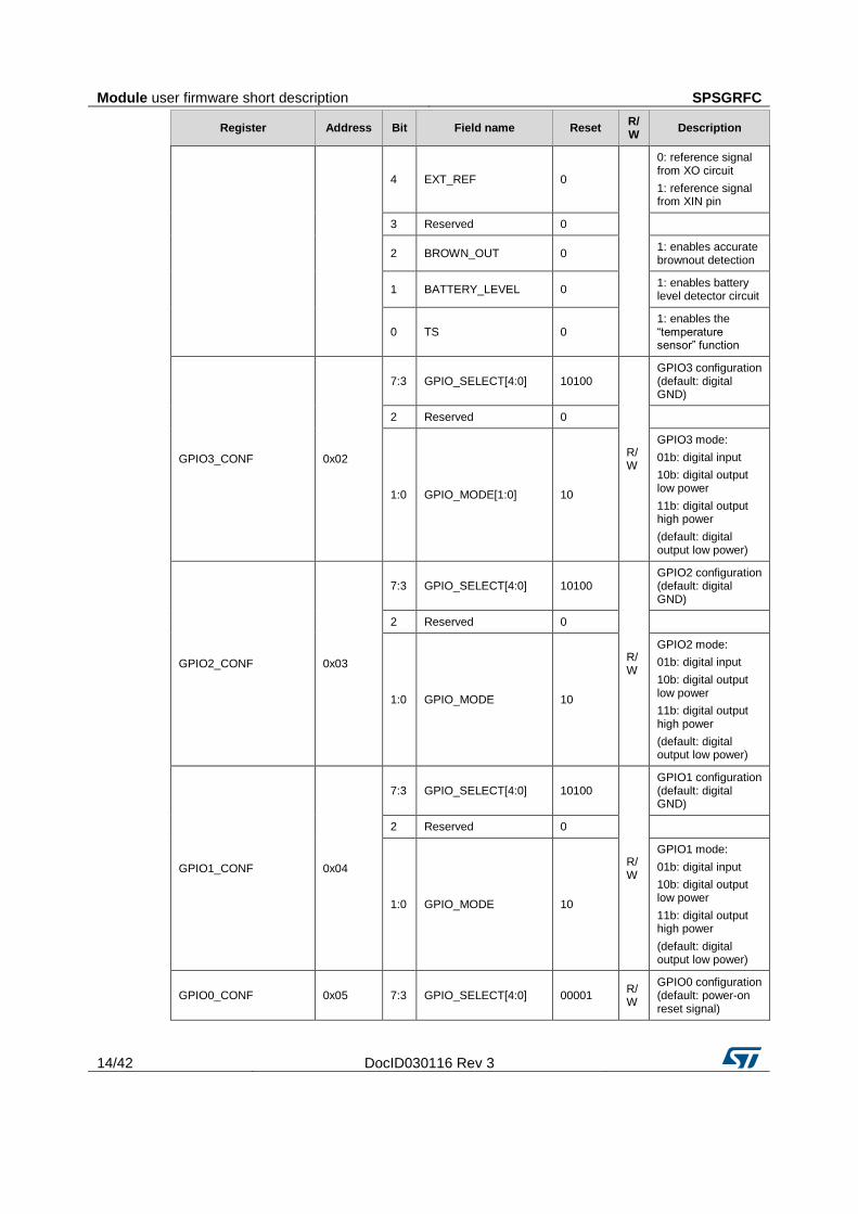
Table 9: General configuration registers
Register Address Bit Field name Reset R/W
Description
ANA_FUNC_CONF[1] 0x00
7:5 Reserved 000
R/W
4:2 GM_CONF[2:0] 011 Sets the driver gm of the XO at startup
1:0 SET_BLD_LVL[1:0] 00
Sets the BLD threshold
00: 2.7 V
01: 2.5 V
10: 2.3 V
11: 2.1 V
ANA_FUNC_CONF[0] 0x01
7 Reserved 1
R/W
6 24_26MHz_SELECT 1
1: 26 MHz configuration
0: 24 MHz configuration
(impact only RCO calibration reference and loop filter tuning)
5 AES_ON 0 1: AES engine enabled
Module user firmware short description SPSGRFC
14/42 DocID030116 Rev 3
Register Address Bit Field name Reset R/W
Description
4 EXT_REF 0
0: reference signal from XO circuit
1: reference signal from XIN pin
3 Reserved 0
2 BROWN_OUT 0 1: enables accurate brownout detection
1 BATTERY_LEVEL 0 1: enables battery level detector circuit
0 TS 0 1: enables the “temperature sensor” function
GPIO3_CONF 0x02
7:3 GPIO_SELECT[4:0] 10100
R/W
GPIO3 configuration (default: digital GND)
2 Reserved 0
1:0 GPIO_MODE[1:0] 10
GPIO3 mode:
01b: digital input
10b: digital output low power
11b: digital output high power
(default: digital output low power)
GPIO2_CONF 0x03
7:3 GPIO_SELECT[4:0] 10100
R/W
GPIO2 configuration (default: digital GND)
2 Reserved 0
1:0 GPIO_MODE 10
GPIO2 mode:
01b: digital input
10b: digital output low power
11b: digital output high power
(default: digital output low power)
GPIO1_CONF 0x04
7:3 GPIO_SELECT[4:0] 10100
R/W
GPIO1 configuration (default: digital GND)
2 Reserved 0
1:0 GPIO_MODE 10
GPIO1 mode:
01b: digital input
10b: digital output low power
11b: digital output high power
(default: digital output low power)
GPIO0_CONF 0x05 7:3 GPIO_SELECT[4:0] 00001 R/W
GPIO0 configuration (default: power-on reset signal)

SPSGRFC Module user firmware short description
DocID030116 Rev 3 15/42
Register Address Bit Field name Reset R/W
Description
2 Reserved 0
1:0 GPIO_MODE 10
GPIO0 mode:
00b: analog
01b: digital input
10b: digital output low power
11b: digital output high power
(default: digital output low power)
MCU_CK_CONF 0x06
7 EN_MCU_CLK 0
R/W
1: The internal divider logic is running, so the MCU clock is available (but proper GPIO configuration is needed)
6:5 CLOCK_TAIL[1:0] 0
Number of extra clock cycles provided to the MCU before switching to STANDBY state:
00: 0 extra clock cycle
01: 64 extra clock cycles
10: 256 extra clock cycles
11: 512 extra clock cycles
4:1 XO_RATIO[3:0] 0 Divider for the XO clock output
0 RCO_RATIO 0
Divider for the RCO clock output
0: 1
1: 1/128
XO_RCO_TEST 0xB4
7:4 Reserved 0010
3 PD_CLKDIV 0
1: disable both dividers of the digital clock (and reference clock for the SMPS) and IF-ADC clock.
2:0 Reserved 001
SYNTH_CONFIG[0] 0x9F 7 SEL_TSPLIT 0 R/
W
0: split time: 1.75 ns
1: split time: 3.47 ns
6:0 Reserved 0100000

Module user firmware short description SPSGRFC
16/42 DocID030116 Rev 3
Register Address Bit Field name Reset R/W
Description
SYNTH_CONFIG[1] 0x9E
7 REFDIV 0
R/W
Enable division by 2 on the reference clock:
0: fREF = fXO frequency
1: fREF = fXO frequency / 2
6:3 Reserved 1011
2 VCO_L_SEL 0 1: enable VCO_L
1 VCO_H_SEL 1 1: enable VCO_H
0 Reserved 1
IF_OFFSET_ANA 0x07 7:0 IF_OFFSET_ANA 0xA3 R/W
Intermediate frequency setting for the analog RF synthesizer.
Table 10: Radio configuration registers (analog blocks)
Register name Address Bit Field name Reset R/W Description
SYNT3 0x08
7:5 WCP[2:0] 000
R/W
Set the charge pump current according to the VCO frequency.
4:0 SYNT[25:21] 01100
SYNT[25:21], highest 5 bits of the PLL programmable divider The valid range depends on fXO and REFDIV settings; for fXO=26MHz.
SYNT2 0x09 7:0 SYNT[20:13] 0x84 R/W
SYNT[20:13], intermediate bits of the PLL programmable divider.
SYNT1 0x0A 7:0 SYNT[12:5] 0xEC R/W
SYNT[12:5], intermediate bits of the PLL programmable divider.
SYNT0 0x0B 7:3 SYNT[4:0] 01010 R/W
SYNT[4:0], lowest bits of the PLL programmable divider.

SPSGRFC Module user firmware short description
DocID030116 Rev 3 17/42
Register name Address Bit Field name Reset R/W Description
2:0 BS 001 R/W
Synthesizer band select. This parameter selects the out-of-loop divide factor of the synthesizer
1: 6 Band select factor for high band
3: 12 Band select factor for middle band
4: 16 Band select factor for low band
5: 32 Band select factor for very low band
CHSPACE 0x0C 7:0 CH_SPACING 0xFC R/W
Channel spacing in steps of fXO/215 (~793 for fXO = 26 MHz, ~732 for fXO = 24 MHz).
IF_OFFSET_DIG 0x0D 7:0 IF_OFFSET_DIG 0xA3 R/W
Intermediate frequency setting for the digital shift-to-baseband
FC_OFFSET[1] 0x0E 7:4 Reserved 0
R/W Carrier offset in steps of fXO/218 and represented as 12 bits 2-complement integer. It is added / subtracted to the carrier frequency set by the SYNTx register. This register can be used to set a fixed correction value obtained e.g. from crystal measurements.
3:0 FC_OFFSET[11:8] 0
FC_OFFSET[0] 0x0F 7:0 FC_OFFSET[7:0] 0 R/W
PA_POWER[8] 0x10 7 Reserved 0
R/W Output power level for 8th slot (+12 dBm) 6:0 PA_LEVEL_7 0000011
PA_POWER[7] 0x11 7 Reserved 0
R/W Output power level for 7th slot (+6 dBm) 6:0 PA_LEVEL_6 0001110
PA_POWER[6] 0x12 7 Reserved 0
R/W Output power level for 6th slot (0 dBm) 6:0 PA_LEVEL_5 0011010
PA_POWER[5] 0x13 7 Reserved 0
R/W Output power level for 5th slot (-6 dBm) 6:0 PA_LEVEL_4 0100101
PA_POWER[4] 0x14 7 Reserved 0
R/W Output power level for 4th slot (-12 dBm) 6:0 PA_LEVEL_3 0110101
PA_POWER[3] 0x15 7 Reserved 0
R/W Output power level for 3rd slot (-18 dBm) 6:0 PA_LEVEL_2 1000000
PA_POWER[2] 0x16 7 Reserved 0
R/W Output power level for 2nd slot (-24 dBm) 6:0 PA_LEVEL_1 1001110
PA_POWER[1] 0x17 7 Reserved 0 R/W Output power level

Module user firmware short description SPSGRFC
18/42 DocID030116 Rev 3
Register name Address Bit Field name Reset R/W Description
6:0 PA_LEVEL_0 0000000 for first slot (-30 dBm)
PA_POWER[0] 0x18 7:6 CWC[1:0] 00
R/W
Output stage additional load capacitors bank (to be used to optimize the PA for different sub-bands):
00: 0 pF
01: 1.2 pF
10: 2.4 pF
11: 3.6 pF
5 PA_RAMP_ENABLE 0
1: enable the power ramping
4:3 PA_RAMP_STEP_WIDTH[1:0] 00
Step width (unit: 1/8 of bit period)
2:0 PA_LEVEL_MAX_INDEX 111
Final level for power ramping or selected output power index.
Table 11: Radio configuration registers (digital blocks)
Register name Address Bit Field name Reset R/W Description
MOD1 0x1A 7:0 DATARATE_M 0x83 R/W The mantissa value of the data rate equation
MOD0 0x1B
7 CW 0
R/W
1: enable the CW transmit mode
6 BT_SEL 0
Select BT value for GFSK
0: BT = 1
1: BT = 0.5
5:4 MOD_TYPE[1:0] 01
Modulation type
0: 2-FSK
1: GFSK
2: ASK/OOK
3: MSK
3:0 DATARATE_E 1010 The exponent value of the data rate equation
FDEV0 0x1C
7:4 FDEV_E[3:0] 0100
R/W
The exponent value of the frequency deviation equation
3 CLOCK_REC_ALGO_SEL 0
Select PLL or DLL mode for symbol timing recovery
2:0 FDEV_M 101
The mantissa value of the frequency deviation

SPSGRFC Module user firmware short description
DocID030116 Rev 3 19/42
Register name Address Bit Field name Reset R/W Description
CHFLT 0x1D
7:4 CHFLT_M[3:0] 0010
R/W
The mantissa value of the channel filter
3:0 CHFLT_E 0011 The exponent value of the channel filter
AFC2 0x1E
7 AFC_FREEZE_ON_SYNC 0 R/W
1: enable the freeze AFC correction upon sync word detection
6 AFC_ENABLE 1
1: enable AFC
5 AFC_MODE 0
Select AFC mode:
0: AFC loop closed on slicer
1: AFC loop closed on second conversion stage
4:0 AFC_PD_LEAKAGE 01000
Peak detector leakage
AFC1 0x1F 7:0 AFC_FAST_PERIOD 0x18 R/W Length of the AFC fast period
AFC0 0x20
7:4 AFC_FAST_GAIN_LOG2[3:0] 0010
R/W
AFC loop gain in fast mode (log2)
3:0 AFC_SLOW_GAIN_LOG2 0101 AFC loop gain in slow mode (log2)
RSSI_FLT 0x21
7:4 RSSI_FLT[3:0] 1110 R/W Gain of the RSSI filter
3:2 CS_MODE 00
Carrier sense mode
1:0 OOK_PEAK_DECAY 11
Peak decay control for OOK: 3 slow decay; 0 fast decay
RSSI_TH 0x22 7:0 RSSI_THRESHOLD 0x24 R/W
Signal detect threshold in 0.5 dB steps,
-120 dBm corresponds to 0x14.
CLOCKREC 0x23
7:5 CLK_REC_P_GAIN[2:0] 2
R/W
Clock recovery loop gain (log2)
4 PSTFLT_LEN 1
Post-filter:
0: 8 symbols,
1: 16 symbols
3:0 CLK_REC_I_GAIN 8
Integral gain for the clock recovery loop (used in PLL mode)
AGCCTRL2 0x24 7:4 Reserved 0010
R/W
3:0 MEAS_TIME 0010 Measure time

Module user firmware short description SPSGRFC
20/42 DocID030116 Rev 3
Register name Address Bit Field name Reset R/W Description
AGCCTRL1 0x25
7:4 THRESHOLD_HIGH[3:0] 0110
R/W
High threshold for the AGC
3:0 THRESHOLD_LOW 0101 Low threshold for the AGC
AGCCTRL0 0x26 7 AGC ENABLE 1
R/W 1: enable AGC.
6:0 Reserved 0001010
ANT_SELECT_CONF 0x27
7:5 Reserved 000
R/W
4 CS_BLANKING 0
1: do not fill the RX FIFO with the data received if the signal is below the CS threshold
3 AS_ENABLE 0 1: enable antenna switching
2:0 AS_MEAS_TIME 101 Measurement time
Table 12: Packet/protocol configuration registers
Register name Address Bit Field name Reset R/W Description
PCKTCTRL4 0x30
7:5 Reserved 000
R/W
4:3 ADDRESS_LEN[1:0] 00
Length of address field in bytes:
0 or 1: Basic
2: STack
2:0 CONTROL_LEN 000 Length of control field in bytes
PCKTCTRL3 0x31
7:6 PCKT_FRMT[1:0] 00
R/W
Format of packet.
0: basic,
2: WM-Bus,
3: STack
5:4 RX_MODE[1:0] 00
RX mode:
0: normal mode,
1: direct through FIFO,
2: direct through GPIO
3:0 LEN_WID 0111 Size in number of binary digit of length field
PCKTCTRL2 0x32
7:3 PREAMBLE_LENGTH[4:0] 00011
R/W
Length of preamble field in bytes (from 1 to 32)
2:1 SYNC_LENGTH[1:0] 11 Length of sync field in bytes (from 1 to 4)
0 FIX_VAR_LEN 0
Packet length mode.
0: fixed,
1: variable (in variable mode the field LEN_WID of PCKTCTRL3 register must be configured)

SPSGRFC Module user firmware short description
DocID030116 Rev 3 21/42
Register name Address Bit Field name Reset R/W Description
PCKTCTRL1 0x33
7:5 CRC_MODE[2:0] 001
R/W
CRC:
0: No CRC,
1: 0x07,
2: 0x8005,
3: 0x1021,
4: 0x864CBF
4 WHIT_EN[0] 0 1: enable the whitening mode on the data
3:2 TXSOURCE[1:0] 00
TX source data:
0: normal mode,
1: direct through FIFO,
2: direct through GPIO,
3: PN9
1 Reserved 0
0 FEC_EN 0
1: enable the FEC encoding in TX or enable the Viterbi decoding in RX
PCKTLEN1 0x34 7:0 PCKTLEN1 0 R/W Length of packet in bytes (MSB)
PCKTLEN0 0x35 7:0 PCKTLEN0 0x14 R/W Length of packet in bytes (LSB)
SYNC4 0x36 7:0 SYNC4 0x88 R/W Sync word 4
SYNC3 0x37 7:0 SYNC3 0x88 R/W Sync word 3
SYNC2 0x38 7:0 SYNC2 0x88 R/W Sync word 2
SYNC1 0x39 7:0 SYNC1 0x88 R/W Sync word 1
QI 0x3A
7:6 SQI_TH[1:0] 00
R/W
SQI threshold
5:2 PQI_TH[3:0] 0000 PQI threshold
1 SQI_EN[0] 1 1: enable SQI
0 PQI_EN[0] 0 1: enable PQI
MBUS_PRMBL 0x3B 7:0 MBUS_PRMBL[7:0] 0x20 R/W MBUS preamble length in chip sequence ‘01’
MBUS_PSTMBL
0x3C 7:0 MBUS_PSTMBL[7:0] 0x20 R/W MBUS postamble length in chip sequence ‘01’
MBUS_CTRL 0x3D
7:4 Reserved 00000
R/W
3:1 MBUS_SUBMODE[2:0] 000
MBUS sub mode: allowed values are 0, 1, 3 and 5
WM-BUS sub mode:
0: S1 S2 long header,
1: S1m S2 T2 other to meter,
3: T1 T2 meter to other,
5: R2 short header
0 Reserved 0
FIFO_CONFIG[3]
0x3E
7 Reserved 0 R/W
6:0 RXAFTHR [6:0] 110000
R/W FIFO almost full threshold for RX FIFO

Module user firmware short description SPSGRFC
22/42 DocID030116 Rev 3
Register name Address Bit Field name Reset R/W Description
FIFO_CONFIG[2]
0x3F
7 Reserved 0 R/W
6:0 RXAETHR [6:0] 110000
R/W FIFO almost empty threshold for RX FIFO
FIFO_CONFIG[1]
0x40
7 Reserved 0 R/W
6:0 TXAFTHR [6:0] 110000
R/W FIFO almost full threshold for TX FIFO
FIFO_CONFIG[0]
0x41
7 Reserved 0 R/W
6:0 TXAETHR [6:0] 110000
R/W FIFO almost empty threshold for TX FIFO
PCKT_FLT_GOALS[12]
0x42 7:0 CONTROL0_MASK 0 R/W For received packet only: all 0s: no filtering on control field
PCKT_FLT_GOALS[11]
0x43 7:0 CONTROL1_MASK 0 R/W For received packet only: all 0s: no filtering on control field
PCKT_FLT_GOALS[10]
0x44 7:0 CONTROL2_MASK 0 R/W For received packet only: all 0s: no filtering on control field
PCKT_FLT_GOALS[9]
0x45 7:0 CONTROL3_MASK 0 R/W For received packet only: all 0s: no filtering on control field
PCKT_FLT_GOALS[8]
0x46 7:0 CONTROL0_FIELD 0 R/W Control field (byte 3) to be used as reference for receiver
PCKT_FLT_GOALS[7]
0x47 7:0 CONTROL1_FIELD 0 R/W Control field (byte 2) to be used as reference for receiver
PCKT_FLT_GOALS[6]
0x48 7:0 CONTROL2_FIELD 0 R/W Control field (byte 1) to be used as reference for receiver
PCKT_FLT_GOALS[5]
0x49 7:0 CONTROL3_FIELD 0 R/W Control field (byte 0) to be used as reference for receiver
PCKT_FLT_GOALS[4]
0x4A 7:0 RX_SOURCE_MASK 0 R/W For received packet only: all 0s: no filtering
PCKT_FLT_GOALS[3]
0x4B 7:0 RX_SOURCE_ADDR 0 R/W RX packet source / TX packet destination fields
PCKT_FLT_GOALS[2]
0x4C 7:0 BROADCAST 0 R/W Broadcast address
PCKT_FLT_GOALS[1]
0x4D 7:0 MULTICAST 0 R/W Multicast address
PCKT_FLT_GOALS[0]
0x4E 7:0 TX_SOURCE_ADDR 0 R/W TX packet source / RX packet destination fields
PCKT_FLT_OPTIONS
0x4F
7 Reserved 0
R/W
6 RX_TIMEOUT_AND_OR_SELECT
1
1: ‘OR’ logical function applied to CS/SQI/PQI values (masked by 7:5 bits in PROTOCOL register: CS_TIMEOUT_MASK, SQI_TIMEOUT_MASK, PQI_TIMEOUT_MASK)

SPSGRFC Module user firmware short description
DocID030116 Rev 3 23/42
Register name Address Bit Field name Reset R/W Description
5 CONTROL_FILTERING 1
1: RX packet accepted if its control fields match with masked CONTROLx_FIELD registers
4 SOURCE_FILTERING 1
1: RX packet accepted if its source field matches with masked RX_SOURCE_ADDR register
3 DEST_VS_SOURCE
_ADDR 0
1: RX packet accepted if its destination address matches with TX_SOURCE_ADDR
reg.
2 DEST_VS_MULTICAST_ADDR
0
1: RX packet accepted if its destination address matches with MULTICAST register
1 DEST_VS_
BROADCAST_ADDR 0
1: RX packet accepted if its destination address matches with BROADCAST
reg.
0 CRC_CHECK 0 1: packet discarded if CRC not valid.
PROTOCOL[2] 0x50
23 CS_TIMEOUT_MASK 0
R/W
1: CS value contributes to timeout disabling
22 SQI_TIMEOUT_MASK 0 1: SQI value contributes to timeout disabling
21 PQI_TIMEOUT_MASK 0 1: PQI value contributes to timeout disabling
20:19
TX_SEQ_NUM_RELOAD[1:0]
0
TX sequence number to be used when counting reset is required using the related command.
18 RCO_CALIBRATION 0 1: enable the automatic RCO calibration
17 VCO_CALIBRATION 1 1: enable the automatic VCO calibration
16 LDC_MODE 0 1: LDC mode on
PROTOCOL[1] 0x51
15 LDC_RELOAD_ON_SYNC 0
R/W
1: LDC timer is reloaded with the value stored in the LDC_RELOAD registers
14 PIGGYBACKING 0 1: PIGGYBACKING enabled
13:12
Reserved 00

Module user firmware short description SPSGRFC
24/42 DocID030116 Rev 3
Register name Address Bit Field name Reset R/W Description
11 SEED_RELOAD 0
1: reload the back-off random generator seed using the value written in the BU_COUNTER_SEED_MSBYTE / LSBYTE registers
10 CSMA_ON 0 1: CSMA channel access mode enabled
9 CSMA_PERS_ON 0 1: CSMA persistent (no back-off) enabled
8 AUTO_PCKT_FLT 0 1: automatic packet filtering mode enabled
PROTOCOL[0] 0x52
7:4 NMAX_RETX[3:0] 0
R/W
Max. number of re-TX (from 0 to 15).
0: re-transmission is not performed
3 NACK_TX 1 1: field NO_ACK=1 on transmitted packet
2 AUTO_ACK 0 1: automatic acknowledgement after correct packet reception
1 PERS_RX 0 1: persistent reception enabled
0 PERS_TX 0 1: persistent transmission enabled
TIMERS[5] 0x53 47:40
RX_TIMEOUT_PRESCALER[7:0]
1 R/W
Prescaler value of the RX TIMEOUT timer. When this timer expires the SPIRIT1 exits RX state. Can be controlled using the quality indicator (SQI, PQI, CS).
TIMERS[4] 0x54 39:32
RX_TIMEOUT_COUNTER[7:0]
0 R/W
Counter value of the RX TIMEOUT timer. When this timer expires the SPIRIT1 exits RX state. Can be controlled using the quality indicator (SQI, PQI, CS)
TIMERS[3] 0x55 31:24
LDC_PRESCALER[7:0] 1 R/W
Prescaler value of the LDC wake-up timer. When this timer expires the SPIRIT1 exits SLEEP state.
TIMERS[2] 0x56 23:16
LDC_COUNTER[7:0] 0 R/W
Counter value of the LDC wake-up timer. When this timer expires the SPIRIT1 exits SLEEP state.

SPSGRFC Module user firmware short description
DocID030116 Rev 3 25/42
Register name Address Bit Field name Reset R/W Description
TIMERS[1] 0x57 15:8 LDC_RELOAD_PRESCALER[7:0]
1 R/W
Prescaler value of the LDC reload timer. When this timer expires the SPIRIT1 exits SLEEP state. The reload timer value is used if the SYNC word is detected (by the receiver) or if the LDC_RELOAD command is used.
TIMERS[0] 0x58 7:0 LDC_RELOAD_COUNTER[7:0]
0 R/W
Counter part of the LDC reload value timer. When this timer expires the SPIRIT1 exits SLEEP state. The reload timer value is used if the SYNC word is detected (by the receiver) or if the LDC_RELOAD command is used.
CSMA_CONFIG[3]
0x64 7:0 BU_COUNTER_SEED_MSBYTE
0xFF R/W
The MSB value of the counter of the seed of the random number generator used to apply the BBE algorithm during the CSMA algorithm
CSMA_CONFIG[2]
0x65 7:0 BU_COUNTER_SEED_LSBYTE
0 R/W
The LSB value of the counter seed of the random number generator used to apply the BBE algorithm during the CSMA algorithm
CSMA_CONFIG[1]
0x66
7:2 BU_PRESCALER[5:0] 000001
R/W
The prescaler value used to program the back-off unit BU
1:0 CCA_PERIOD 00 Used to program the Tcca time (64 / 128 / 256 / 512 × Tbit)
CSMA_CONFIG[0]
0x67
7:4 CCA_LENGTH[3:0] 0000
R/W
Used to program the Tlisten time
3 Reserved 0
2:0 NBACKOFF_MAX 000 Max. number of back-off cycles
TX_CTRL_FIELD[3]
0x68 7:0 TX_CTRL3 0 R/W Control field value to be used in TX packet as byte n.3
TX_CTRL_FIELD[2]
0x69 7:0 TX_CTRL2 0 R/W Control field value to be used in TX packet as byte n.2
TX_CTRL_FIELD[1]
0x6A 7:0 TX_CTRL1 0 R/W Control field value to be used in TX packet as byte n.1
TX_CTRL_FIELD[0]
0x6B 7:0 TX_CTRL0 0 R/W Control field value to be used in TX packet as byte n.0

Module user firmware short description SPSGRFC
26/42 DocID030116 Rev 3
Register name Address Bit Field name Reset R/W Description
PM_CONFIG[2] 0xA4
7 Reserved 0
R/W
6 EN_TS_BUFFER 0 1: temperature sensor output is buffered
5 DISABLE_SMPS 0
0: enable internal SMPS
1: disable internal SMPS
4 Reserved 0
3 SET_SMPS_VTUNE 1 Sets the SMPS Vtune voltage
2 SET_SMPS_PLLBW 1 Sets the SMPS bandwidth
1:0 Reserved 00
PM_CONFIG[1] 0xA5
7 EN_RM 0
R/W
0: divider by 4 enabled (SMPS' switching frequency is FSW=FOSC/4)
1: rate multiplier enabled (SMPS' switching frequency is FSW=KRM*FOSC/(2^15)
6:0 KRM[14:8] 0100000 Sets the divider ration of
the rate multiplier. PM_CONFIG[0] 0xA6 7:0 KRM[7:0] 0 R/W
XO_RCO_CONFIG
0xA7
7:4 Reserved 1110
R/W
3 EXT_RCOSC 0 1: the 34.7kHz signal must be supplied from a GPIO pin
2:0 Reserved 001
TEST_SELECT 0xA8 7:0 Reserved 0x00 R/W
PM_TEST 0xB2 7:0 Reserved 0x42
Table 13: Frequently used registers
Register name Address Bit Field name Reset R/W Description
CHNUM 0x6C 7:0 CH_NUM 0 R/W
Channel number. This value is multiplied by the channel spacing and added to the synthesizer base frequency to generate the actual RF carrier frequency.
VCO_CONFIG 0xA1
7:6 Reserved 00
R/W
5:0 VCO_GEN_CURR
010001
Set the VCO current
RCO_VCO_CALIBR_IN[2]
0x6D 7:4 RWT_IN[3:0] 0111
R/W
RWT word value for the RCO
3:0 RFB_IN[4:1] 0000 RFB word value for the RCO
RCO_VCO_CALIBR_IN[1]
0x6E
7 RFB_IN[0] 0
R/W 6:0
VCO_CALIBR_TX[6:0]
1001000
Word value for the VCO to be used in TX mode

SPSGRFC Module user firmware short description
DocID030116 Rev 3 27/42
Register name Address Bit Field name Reset R/W Description
RCO_VCO_CALIBR_IN[0]
0x6F
7 Reserved 0
R/W
6:0 VCO_CALIBR_RX[6:0]
1001000
Word value for the VCO to be used in RX mode
AES_KEY_IN[15] 0x70 7:0 AES_KEY15 0 R/W AES engine key input (128 bits)
AES_KEY_IN[14] 0x71 7:0 AES_ KEY14 0 R/W AES engine key input (128 bits)
… 7:0 … … … …
AES_KEY_IN[1] 0x7E 7:0 AES_ KEY1 0 R/W AES engine key input (128 bits)
AES_KEY_IN[0] 0x7F 7:0 AES_ KEY0 0 R/W AES engine key input (128 bits)
AES_DATA_IN[15] 0x80 7:0 AES_IN15 0 R/W AES engine data input (128 bits)
AES_DATA_IN[14] 0x81 7:0 AES_IN14 0 R/W
AES engine data input (128 bits)
… … … … … …
AES_DATA_IN[1] 0x8E 7:0 AES_IN1 0 R/W AES engine data input (128 bits)
AES_DATA_IN[0] 0x8F 7:0 AES_IN0 0 R/W AES engine data input (128 bits)
IRQ_MASK[3] 0x90 7:0 INT_MASKT[31:24]
0 R/W The IRQ mask register to route the IRQ information to a GPIO.
IRQ_MASK[2] 0x91 7:0 INT_MASK [23:16]
0 R/W The IRQ mask register to route the IRQ information to a GPIO.
IRQ_MASK[1] 0x92 7:0 INT_MASK[15:8] 0 R/W The IRQ mask register to route the IRQ information to a GPIO.
IRQ_MASK[0] 0x93 7:0 INT_MASK [7:0] 0 R/W The IRQ mask register to route the IRQ information to a GPIO.
DEM_CONFIG 0xA3
7:2 Reserved 001101
R/W
Reserved do not modify
1 DEM_ORDER 1 Set it to 0 during radio initialization
0 Reserved 1 Reserved do not modify
PM_CONFIG 0xA4
7 Reserved 0
R/W
6 EN_TS_BUFFER 0 1: temperature sensor output is buffered
5 DISABLE_SMPS 0 0: enable internal SMPS
1: disable internal SMPS
MC_STATE[1] 0xC0
7:4 Reserved 0101
R
3 ANT_SELECT 0 Currently selected antenna
2 TX_FIFO_FULL 0 1: TX FIFO is full
1 RX_FIFO_EMPTY 0 1: RX FIFO is empty
0 ERROR_LOCK 0 1: RCO calibrator error

Module user firmware short description SPSGRFC
28/42 DocID030116 Rev 3
Register name Address Bit Field name Reset R/W Description
MC_STATE[0] 0xC1 7:1 STATE[6:0] 0
R Current MC state.
0 XO_ON 0 1: XO is operating
TX_PCKT_INFO 0xC2
7:6 Reserved 0
R
5:4 TX_SEQ_NUM 0 Current TX packet sequence number
3:0 N_RETX 0
Number of transmission done at the end of a TX sequence. The value is updated to the max. number of retransmission reached or at the reception of an ACK packet.
RX_PCKT_INFO 0xC3
7:3 Reserved 0
R
2 NACK_RX 0 NACK field of the received packet
1:0 RX_SEQ_NUM 0 Sequence number of the received packet
AFC_CORR 0xC4 7:0 AFC_CORR[7:0] 0 R AFC word of the received packet
LINK_QUALIF[2] 0xC5 7:0 PQI[7:0] 0 R PQI value of the received packet
LINK_QUALIF[1] 0xC6
7 CS 0
R
Carrier sense indication
6:0 SQI[6:0] 0 SQI value of the received packet
LINK_QUALIF[0] 0xC7
7:4 Reserved 0
R
3:0 AGC_WORD 0 AGC word of the received packet
RSSI_LEVEL 0xC8 7:0 RSSI_LEVEL 0 R RSSI level of the received packet
RX_PCKT_LEN[1] 0xC9 7:0 RX_PCKT_LEN1 0 R Length (number of bytes) of the received packet:
RX_PCKT_LEN=RX_PCKT_LEN1 × 256 + RX_PCKT_LEN0
RX_PCKT_LEN[0] 0xCA 7:0 RX_PCKT_LEN0 0 R
CRC_FIELD[2] 0xCB 7:0 CRC2 0 R CRC field of the received packet, byte 2
CRC_FIELD[1] 0xCC 7:0 CRC1 0 R CRC field of the received packet, byte 1
CRC_FIELD[0] 0xCD 7:0 CRC0 0 R CRC field of the received packet, byte 0
RX_CTRL_FIELD[3] 0xCE 7:0 RX_CTRL0 0 R Control field(s) of the received packet, byte 0
RX_CTRL_FIELD[2] 0xCF 7:0 RX_CTRL1 0 R Control field(s) of the received packet, byte 1
RX_CTRL_FIELD[1] 0xD0 7:0 RX_CTRL2 0 R Control field(s) of the received packet, byte 2
RX_CTRL_FIELD[0] 0xD1 7:0 RX_CTRL3 0 R Control field(s) of the received packet, byte 3
RX_ADDR_FIELD[1] 0xD2 7:0 ADDR1 0 R Source address field of the RX packet.

SPSGRFC Module user firmware short description
DocID030116 Rev 3 29/42
Register name Address Bit Field name Reset R/W Description
RX_ADDR_FIELD[0] 0xD3 7:0 ADDR0 0 R Destination address field of the RX packet.
AES_ DATA_OUT[15] 0xD4 7:0 AES_OUT15 0 R AES engine data output (128 bits)
AES_ DATA_OUT[14] 0xD5 7:0 AES_OUT14 0 R
AES engine data output (128 bits)
… … … … … …
AES_ DATA_OUT[1] 0xE2 7:0 AES_OUT1 0 R AES engine data output (128 bits)
AES_ DATA_OUT[0] 0xE3 7:0 AES_OUT0 0 R AES engine data output (128 bits)
RCO_VCO_CALIBR_OUT[1]
0xE4
7:4 RWT_OUT[3:0] 0
R
RWT word from internal RCO calibrator
3:0 RFB_OUT[4:1] 0 RFB word from internal RCO calibrator
RCO_VCO_CALIBR_OUT[0]
0xE5
7 RFB_OUT[0] 0
R
6:0 VCO_CALIBR_DATA
0 Output word from internal VCO calibrator
LINEAR_FIFO_STATUS[1]
0xE6
7 Reserved 0
R
6:0 ELEM_TXFIFO 0 Number of elements in the linear TX FIFO (from 0 to 96 bytes)
LINEAR_FIFO_STATUS[0]
0xE7
7 Reserved 0
R
6:0 ELEM_RXFIFO 0 Number of elements in the linear RX FIFO (from 0 to 96 bytes)
IRQ_STATUS[3] 0xFA 7:0 INT_EVENT[31:24]
0 RR The IRQ status register.
IRQ_STATUS[2] 0xFB 7:0 INT_EVENT[23:16]
0 RR The IRQ status register.
IRQ_STATUS[1] 0xFC 7:0 INT_EVENT[15:8] 0 RR The IRQ status register.
IRQ_STATUS[0] 0xFD 7:0 INT_EVENT[7:0] 0 RR The IRQ status register.
DEVICE_INFO[1:0] 0xF0 7:0 PARTNUM[7:0] 0x01 R Device part number
0xF1 7:0 VERSION[7:0] 0x30 R Device version number

Regulatory compliance SPSGRFC
30/42 DocID030116 Rev 3
8 Regulatory compliance
8.1 RF compliance
The RF certifications obtained are described in table below.
Table 14: RF certification summary
ID Part Comment
FCC ID
S9NSPSGRFC With external “TAOGLASS” antenna and UFL to SMA connector RF cable version
IC ID 8976C-
SPSGRFC With external “TAOGLASS” antenna and UFL to SMA connector RF cable version
ETSI Compliant Approved with external “LINX” antenna an d UFL to SMA cable version
This radio transmitter IC ID 8976-SPSGRFC has been approved by Industry Canada to operate with the antenna types listed below with the maximum permissible gain indicated.
Antenna types not included in this list, having a gain greater than the maximum gain indicated for that type, are strictly prohibited for use with this device.
The “TI.19.2113” antenna from “TAOGLASS” is the only approved antenna using the u.fl connector version.
8.2 SPSGRFC-915 module approved antenna
For SPSGRFC-915, the approved antenna is the TAOGLASS TI.19.2113.
Below is an extract from the antenna datasheet: TI.19 is a high performance 915 MHz ISM band dipole omni-directional antenna.
The hinged design enables the antenna to be positioned at its most suitable angle. This antenna features a SMA(M) Plug Connector.
For a lot of antenna applications such as Wi-Fi Hotspot or cellular Pico-cell, the antenna of the operator’s device and the antenna of the user’s remote device are not on the same horizontal level. The TI.19 has been designed with a butterfly shape radiation pattern to help counteract this effect.
Table 15: TAOGLASS TI.19.2113 specifications
Electrical
Frequency 902 ~ 928MHz
Peak gain (bend) 2.5dBi
Peak gain (straight) 2.4dBi
Average gain (bend) -1.0dBi
Average gain (straight) -0.9dBi
Efficiency (bend) 81%
Efficiency (straight) 82%

SPSGRFC Regulatory compliance
DocID030116 Rev 3 31/42
Impedance 50Ω
VSWR < 1.9 : 1
Polarization Linear
Radiation Pattern Omni
Input Power 10 W
Mechanical
Antenna Length 389 ± 5 mm
Antenna Diameter 13 ± 0.5 mm
Casing TPU
Connector SMA Male
Environmental
Temperature Range -40°C to 85°C
Humidity Non-condensing 65°C 95% RH
all data provided in this table are based on the “TAOGLASS TI.19.2113” reference documentation.
8.3 SPSGRFC-868 module approved antenna
For the SPSGRFC-868 module the approved antenna is the LINX ANT-868-CW-QW. Below is an extract from the antenna datasheet:

Regulatory compliance SPSGRFC
32/42 DocID030116 Rev 3
Figure 7: SPSGRFC-868 antenna
Table 16: Ordering information
Order code
ANT-868-CW-QW (with RP-SMA connector)
ANT-868-CW-QW-SMA (with SMA connector)
Product description
CW Series ¼-wave antennas deliver outstanding performance in a rugged and cosmetically attractive package. These antennas are available with standard SMA or FCC Part 15 compliant RP-SMA connectors. RP-SMA connectors allow for easy field replacement while complying with FCC requirements. A wide variety of matching connectors permit numerous mounting options.

SPSGRFC Regulatory compliance
DocID030116 Rev 3 33/42
Features
Low cost
Excellent performance
Omni-directional pattern
Wide bandwidth
Very low VSWR
Fully weatherized
Flexible main shaft
Rugged & damage-resistant
SMA or Part 15 compliant RP-SMA connector
Use with plastic (requires proximity ground plane) or metal enclosures
Electrical specifications
Center frequency: 868 MHz
Recom. freq. range: 750 - 950 MHz
Wavelength: ¼-wave
Peak gain: 1.6 dBi
VSWR: < 1.9 typ. at center
Impedance: 50 Ω
Connector: RP-SMA or SMA
Oper. temp. range: – 40 °C to + 90 °C
Electrical specifications and plots measured on 10.16 cm x 10.16 cm (4.00” x 4.00”) reference ground plane
all data provided in this table are based on the “LINX - ANT-868-CW-QW ” reference ground plane.
8.4 SPSGRFC-433 module approved antenna
For the SPSGRFC-433 module the approved antenna is the LINX ANT-433-CW-QW. Below is an extract from the antenna datasheet:

Regulatory compliance SPSGRFC
34/42 DocID030116 Rev 3
Figure 8: SPSGRFC-433 antenna
Table 17: Ordering information
Order code
ANT-433-CW-QW (with RP-SMA connector)
ANT-433-CW-QW-SMA (with SMA connector)
Product description
CW Series ¼-wave antennas deliver outstandingperformance in a rugged and cosmetically attractive package. These antennas are available with standard SMA or FCC Part 15 compliant RP-SMA connectors. RP-SMA connectors allow for easy field replacement while complying with FCC requirements. A wide variety of matching connectors permit numerous mounting options.

SPSGRFC Regulatory compliance
DocID030116 Rev 3 35/42
Features
Low cost
Excellent performance
Omni-directional pattern
Wide bandwidth
Very low VSWR
Fully weatherized
Flexible main shaft
Rugged & damage-resistant
SMA or Part 15 compliant RP-SMA connector
Use with plastic (requires proximity ground plane) or metal enclosures
Electrical specifications
Center frequency: 433 MHz
Recom. freq. range: 400 - 470 MHz
Wavelength: ¼-wave
Peak gain: 3.3 dBi
VSWR: < 1.9 typ. at center
Impedance: 50 Ω
Connector: RP-SMA or SMA
Oper. temp. range: – 40 °C to + 90 °C
Electrical specifications and plots measured on 10.16 cm x 10.16 cm (4.00” x 4.00”) reference ground plane
all data provided in this table are based on the “LINX - ANT-433-CW-QW ” reference ground plane.
8.5 FCC and IC
The SPSGRFC-915 module has been tested and complies with the FCC part 15 and IC RSS-247 regulations. These limits are designed to provide reasonable protection against harmful interference in approved installations. This equipment generates, uses, and can radiate radio frequency energy and, if not installed and used in accordance with the instructions, may cause harmful interference to radio communications.
However, there is no guarantee that interference will not occur in a particular installation. This device complies with part 15 of the FCC rules. Operation is subject to the following two conditions:
The device must not cause harmful interference and
The device must accept any interference received, including interference that may cause undesired operation
Modifications or changes to this equipment not expressly approved by the party responsible for compliance may render void the user's authority to operate this equipment.
Modular approval, FCC and IC
FCC ID: S9NSPSGRFC
IC: 8976C-SPSGRFC
In accordance with FCC part 15, the module SPSGRFC-915 is listed above as a modular transmitter device.

Regulatory compliance SPSGRFC
36/42 DocID030116 Rev 3
8.5.1 Labeling instructions
When integrating the SPSGRFC-915 into the final product, ensure that the FCC and IC labeling requirements specified below are satisfied. Based on the Public Notice from FCC, the product into which the ST transmitter module is installed must display a label referring to the enclosed module. The label should use wording like the following:
Contains transmitter module
- FCC ID: S9NSPSGRFC
- IC: 8976C-SPSGRFC
Any similar wording that expresses the same meaning may also be used.
8.6 CE Certification
The SPSGRFC-868 and SPSGRFC-433 have been certified according to the following certification rules:
– EN 300 328 V 2.1.1 (2016-11) (1)
– ETSI EN 301 489-17 V3.1.1 (2017-02) (2)
– ETSI EN 301 489-1 V2.1.1 (2017-02) (3)
– EN 60950-1:2006 + A11:2009 + A1:2010 + A12:2011 + A2:2013 (4)
- EN 62479:2010
1. EN 300 328 V 2.1.1 (2016 11): “electromagnetic compatibility and radio spectrum Matters (ERM); Wideband transmission systems; data transmission equipment operating in the 2.4 GHZ ISM band and using wideband modulation techniques; harmonized EN covering essential requirements under article 3.2 of the R&TTE directive”.
2. EN 301 489-17 V 3.1.1 (2017 02): “electromagnetic compatibility and radio spectrum Matters (ERM); electromagnetic compatibility (EMC) standard for radio equipment and services; part 17: specific condition for 2.4 GHz wideband transmission systems and 5 GHz high performance RLAN equipment”.
3. ETSI EN 301 489-1 V2.1.1 (2017 02): “electromagnetic compatibility and radio spectrum Matters (ERM); electromagnetic compatibility (EMC) standard for radio equipment and services; part 1: Common technical requirements”.
4. EN60950-1:2006 +A11:2009+A1:2010+A12:2011+A2:2013: “Information technology equipment - safety”.
The modules are provided by CE marking:
Figure 9: CE marking
The modules have obtained the RED certificate: No. 0051-RED-0029 REV. 0”

SPSGRFC Regulatory compliance
DocID030116 Rev 3 37/42
The certified modules test platforms are based on STSW-SP1ML868AT production firmware release:
1.X
For additional information please refer to:
STMicroelectronics Via C. Olivetti 2, Agrate Brianza 20864 (ITALY)

RoHS compliance SPSGRFC
38/42 DocID030116 Rev 3
9 RoHS compliance
ST Bluetooth modules comply with the ECOPACK2 level of RoHS compliance grade.

SPSGRFC Traceability
DocID030116 Rev 3 39/42
10 Traceability
Each module is univocally identified by serial number stored in a 2D data matrix laser marked on the bottom side of the module itself.
The serial number has the following format:
WW YY D FF NNN
where
WW = week
YY = year
D = product ID family
FF = production panel coordinate identification
NNN = progressive serial number.
Each module bulk is identified by a bulk ID.
BULK ID and module 2D data matrix are linked by a reciprocal traceability link.
The module 2D data matrix traces the lot number of any raw material used.

Ordering information SPSGRFC
40/42 DocID030116 Rev 3
11 Ordering information Table 18: Ordering information
Order code Description Packing MOQ
SPSGRFC-433 433 MHz Spirit1 transceiver module (Region 1, Europe)
Jedec tray 2448 pcs
SPSGRFC-868 868 MHz Spirit1 transceiver module (Region 1, Europe)
Jedec tray 2448 pcs
SPSGRFC-915 915 MHz Spirit1 transceiver module (Region 2, the Americas)
Jedec tray 2448 pcs

SPSGRFC Revision history
DocID030116 Rev 3 41/42
12 Revision history Table 19: Document revision history
Date Version Changes
02-Mar-2017 1 Initial release.
25-May-2017 2 Updated Table 6: "RF compliance limits table".
25-Oct-2017 3 Updated figure on the cover page and Section 4: "Mechanical dimensions".

SPSGRFC
42/42 DocID030116 Rev 3
IMPORTANT NOTICE – PLEASE READ CAREFULLY
STMicroelectronics NV and its subsidiaries (“ST”) reserve the right to make changes, corrections, enhancements, modifications , and improvements to ST products and/or to this document at any time without notice. Purchasers should obtain the latest relevant information on ST products before placing orders. ST products are sold pursuant to ST’s terms and conditions of sale in place at the time of order acknowledgement.
Purchasers are solely responsible for the choice, selection, and use of ST products and ST assumes no liability for application assistance or the design of Purchasers’ products.
No license, express or implied, to any intellectual property right is granted by ST herein.
Resale of ST products with provisions different from the information set forth herein shall void any warranty granted by ST for such product.
ST and the ST logo are trademarks of ST. All other product or service names are the property of their respective owners.
Information in this document supersedes and replaces information previously supplied in any prior versions of this document.
© 2017 STMicroelectronics – All rights reserved


![Using the SPIRIT1 transceiver with range extender under … · Using the SPIRIT1 transceiver with range extender ... 220 [2]. The same SAW filter ... Using the SPIRIT1 transceiver](https://static.fdocuments.net/doc/165x107/5adf6f4d7f8b9ac0428c2a02/using-the-spirit1-transceiver-with-range-extender-under-the-spirit1-transceiver.jpg)