Studying quantum physics in atomically thin van der Waals ... · Studying quantum physics in...
9
Studying quantum physics in atomically thin van der Waals crystals Dong-Keun Ki
Transcript of Studying quantum physics in atomically thin van der Waals ... · Studying quantum physics in...

Studying quantum physics in atomically
thin van der Waals crystals
Dong-Keun Ki

Transport of many quantum particles (1016-24 cm-3) in a mesoscopic scale
Quantum-to-Classical physicsQuantum coherence & correlations,
Fluctuations, Band-structure topology, …
Low-temperature mesoscopic quantum physics
Dong-Keun Ki 2Introduction
Å 10-10 m
nm 10-9 m
mm 10-6 m
mm 10-3 m
m 100 m
Quantum physics(𝐻𝜓 = 𝐸𝜓)
Classical physics(𝐹 = 𝑚𝑎)
• Nano-electronic device fabrication
mK 10-6 K
mK 10-3 K
100 K
103 K
106 K
High-energy physics- LHC (1012 K)
- Supernova (~105 K)- Sun (5777 K)
Ultra cold atoms: dilute (~1014 cm-3)
Image from Lens
Image from NASA
Image from Google
• Cryogenics• Low-noise
measurement
Direct study
Final project Final project

van der Waals coupled layered materials → defect-free monolayers
Dong-Keun Ki 3Introduction
In graphite, each graphene layers are coupled by a van der Waals (vdW) forcewhich is much weaker than chemical bonds.
Thus, it can be exfoliated to produce “defect-free” atomically thin layers
van der Waals interaction
Graphite GrapheneMechanical,
Chemical
Massless Dirac electrons
Charge neutrality point (CNP)
N=0
Characteristic N=0 Landau level
Direct study

N-layer graphene: a family of closely related electronic systems
Electronic properties vary with atomic structures.Different from conventional 2D electron gas systems.
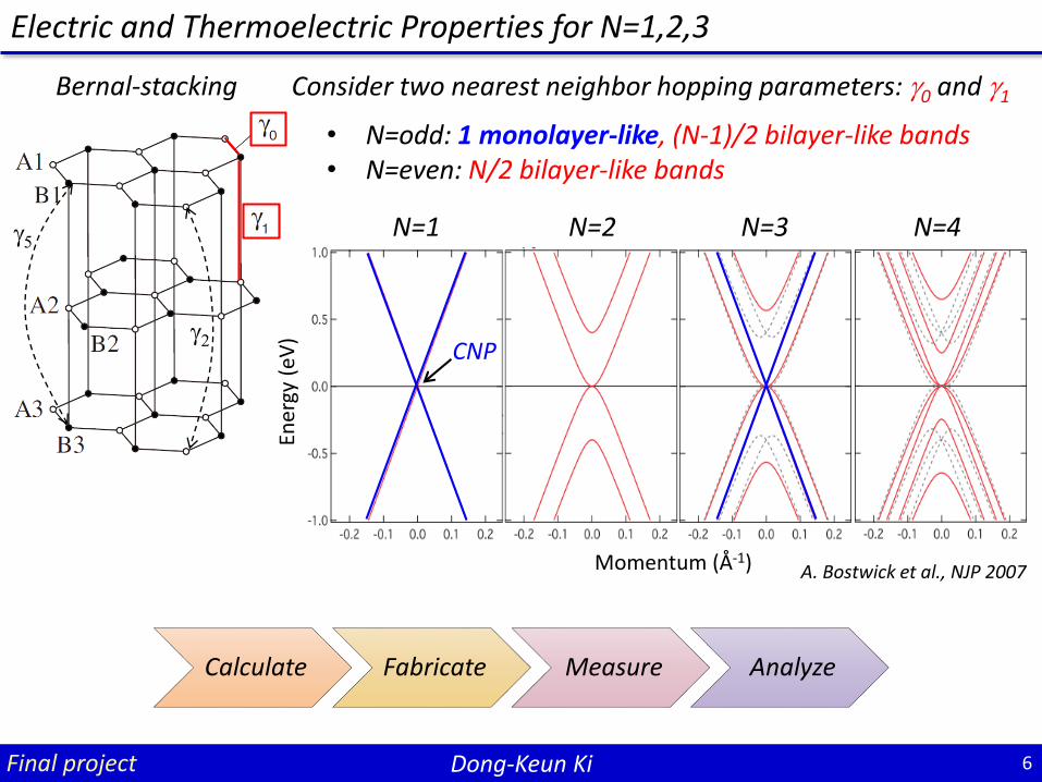
Consider two nearest neighbor hopping parameters: g0 and g1
Bernal-stacking
N=1 N=2 N=3 N=4
Ener
gy (
eV)
Momentum (Å-1) A. Bostwick et al., NJP 2007
CNP
• N=odd: 1 monolayer-like, (N-1)/2 bilayer-like bands• N=even: N/2 bilayer-like bands
Dong-Keun KiIntroduction 4
Final project
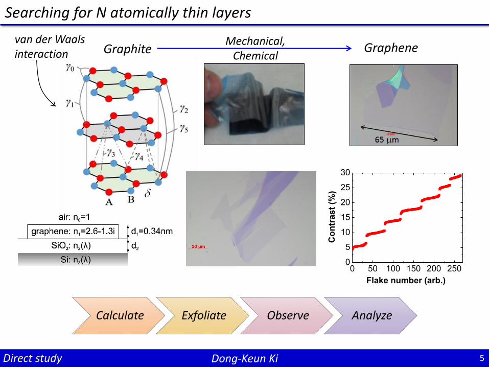
Searching for N atomically thin layers
Dong-Keun Ki 5Direct study
van der Waals interaction Graphite Graphene
Mechanical, Chemical
Calculate Exfoliate Observe Analyze
0 50 100 150 200 2500
5
10
15
20
25
30
Co
ntr
ast
(%)
Flake number (arb.)
g2
g5
Electric and Thermoelectric Properties for N=1,2,3
Consider two nearest neighbor hopping parameters: g0 and g1Bernal-stacking
N=1 N=2 N=3 N=4
Ener
gy (
eV)
Momentum (Å-1) A. Bostwick et al., NJP 2007
CNP
• N=odd: 1 monolayer-like, (N-1)/2 bilayer-like bands• N=even: N/2 bilayer-like bands
Dong-Keun KiFinal project 6
Calculate Fabricate Measure Analyze

Electric and Thermoelectric Properties for N=1,2,3
Dong-Keun KiFinal project 7
Electric quantities : electric currents or voltages
Thermodynamic quantities : temperature or entropy
DV
f(E)
E
EF
f(E)
E
Thermoelectric effect
@ T, B, VG, P
Th Tc
(DT = Th-TC)S = -DV/DT
S depends sensitively on how E changes with electron density (n)
𝑆 ∝𝜕 ln 𝜎 𝐸
𝜕𝐸∝1
𝜎
𝑑𝜎
𝑑𝑛
𝑑𝑛
𝑑𝐸
Mott relation

2D family: layered materials that can be tinned down to atomic-layers
Dong-Keun Ki 8Conclusion
Graphene family(hexagonal layers)
Graphene layers
hBN layers
2D chalcogenides(MX, MX2, M2X3, etc)
2D dichalcogenides (MX2)
SemiconductingSemimetallicSuperconducting
MX: layered semiconductors(GaSe, GaTe, InSe, …)
Bi2Se3: topological insulator
and others….
Buckled graphene
Back phosphorus
2D oxides
Bi-2212 MnO2
Magnetic materialsCrI3 ; 2H-VSe2
Cr1/3NbS2
etc
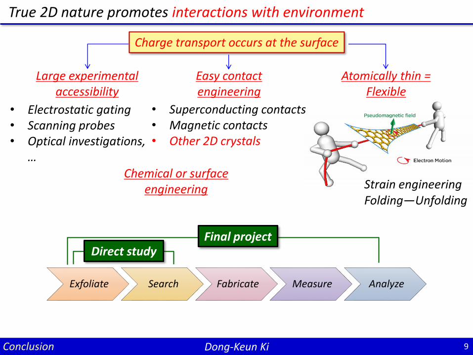
True 2D nature promotes interactions with environment
Dong-Keun Ki 9Conclusion
Charge transport occurs at the surface
Easy contact engineering
Atomically thin = Flexible
Large experimental accessibility
• Electrostatic gating• Scanning probes• Optical investigations,
…
• Superconducting contacts• Magnetic contacts• Other 2D crystals
Strain engineeringFolding—Unfolding
Chemical or surface engineering
Exfoliate Search Fabricate Measure Analyze
Direct studyFinal project