Study on Three-level DC/DC Converter with Coupled … on Three-level DC/DC Converter with Coupled...
115
Study on Three-level DC/DC Converter with Coupled Inductors Ruiyang Qin Thesis submitted to the faculty of the Virginia Polytechnic Institute and State University in partial fulfillment of the requirements for the degree of Master of Science In Electrical Engineering Fred C. Lee, Chair Qiang Li Rolando Burgos September 6 th , 2016 Blacksburg, Virginia Keywords: Coupled inductors, Magnetic Integration, Multi- phase Three-level DC/DC, Interleaving ©2016, Ruiyang Qin
-
Upload
hoangquynh -
Category
Documents
-
view
220 -
download
2
Transcript of Study on Three-level DC/DC Converter with Coupled … on Three-level DC/DC Converter with Coupled...

Study on Three-level DC/DC Converter with
Coupled Inductors
Ruiyang Qin
Thesis submitted to the faculty of the
Virginia Polytechnic Institute and State University in partial fulfillment of the requirements for the degree of
Master of Science
In
Electrical Engineering
Fred C. Lee, Chair
Qiang Li
Rolando Burgos
September 6th
, 2016
Blacksburg, Virginia
Keywords: Coupled inductors, Magnetic Integration, Multi-
phase Three-level DC/DC, Interleaving
©2016, Ruiyang Qin
Study on Three-level DC/DC Converter with
Coupled Inductors
Ruiyang Qin
(Abstract)
High power multi-level converters are deemed as the mainstay power conversion
technology for renewable energy systems including the battery storage system, PV farm and
electrical vehicle charge station. This thesis is focused on the study of three-level DC/DC converter
with multi-phase interleaved structure, with coupled and integrated magnetics to achieve high
power density. The proposed interleaved phased legs offer the benefit of output current ripple
reduction, while inversed coupled inductors can suppress the circulating current between phase
legs. Compared with conventional non-interleaving three-level DC/DC converter with non-
coupling inductors, both inductor current ripple and output current ripple are largely reduced by
interleaving with inverse-coupled inductors.
Because of the non-linearity of the inductor coupling, the equivalent circuit model is
developed for the proposed interleaving structure. The model identifies the existence of multiple
equivalent inductances during one switching cycle. A combination of them determines the inductor
current ripple and dynamics of the system. By virtue of inverse coupling and means of controlling
the coupling coefficients, one can minimize the current ripple and the unwanted circulating current.

To further reduce the magnetic volume, the four inductors in two-phase three-level DC/DC
converter are integrated into one common structure, incorporating the negative coupling effects.
The integrated magnetic structure can effectively suppress the circulating current and reduce the
inductor current ripple and it is easy to manufacture. This thesis provides an equivalent circuit
model to facilitate the design optimization of the integrated system.
A prototype of integrated coupled inductors is assembled with nano-crystalline C-C core
and powder block core. It is tested with both impedance analyzer and single pulse tester, to
guarantee proper mutual inductance for inductor current ripple and output current ripple target.
With a two-phase three-level DC/DC converter hardware, the concept of integrated coupled
inductors is verified, showing its good performance in high-voltage, high-power conversion
applications.
Study on Three-level DC/DC Converter with
Coupled Inductors
Ruiyang Qin
(General Audience Abstract)
With the demanding energy consumption globally, there is an increasing trend for the
requirement of high efficiency power converters with high power density. The application for
renewable energies including the PV farm, battery storage system and electrical vehicle become
more and more important for the sustainable development of society. High-power, high-voltage
DC/DC converters can fulfill the role for such renewable energy power conversion. In this paper,
a multi-phase multi-level DC/DC converter solution suitable for high-power, high-voltage
application is analyzed and designed. With the techniques including interleaving operation and
inverse coupled inductors, the power density for the power conversion is increased while keeping
a high system efficiency.
The discussed power converter in this thesis demonstrated a solution for high-power, high-
voltage DC/DC power conversion with high efficiency. And the concept is verified with real
hardware experimental results, showing its good performance for a 200kW power conversion
system.

v
Acknowledgement
First of all, I would like to express my deepest gratitude for my advisor, Professor Fred C.
Lee, for his generous and inspiring instruction, guidance and support for my study at Center for
Power Electronics System for the past three years. Dr. Lee’s instruction is a precious treasure for
me, and I am benefited not only in intellectual aspect, but also for logic thinking and earnest
attitude toward research and everything in everyday life. I believe I’ll be blessed in the future work
because of my experience studying with Dr. Lee in CPES.
I also would like to thank Dr. Dushan Boroyevich, Dr. Rolando Burgos, and Dr. Qiang Li,
for their instructions and guidance within the Renewable Energy and Nanogrids (REN) group.
Their kind and honest suggestions for my work gives me more in-depth understanding and idea of
research.
I would like to appreciate all the colleagues and students from CPES: Dr. Yang Jiao, Dr.
Mingkai Mu, Dr. Lingxiao Xue, Mr. Wei Zhang, Dr. Zhemin Zhang, Mr. Xiucheng Huang, Mr.
Zhengyang Liu, Mr. Jun Wang, Mr. Ming Lv, Mr. Yuchen Yang, Mr. Dongbin Hou, Mr. Chao Fei,
Mr. Qiong Wang, Mr. Fang Chen, Mr. Chi Li, Ms. Rashidi Mehrabadi Niloofar, Mr. Yadong Lv,
Mr. Yi-Hsun Hsieh. I also want to thank Mr. Bin Li, Mr. Shishuo Zhao, Mr. Chen Li, Mr. Tinge
Ge, Ms. Bingyao Sun, Mr. Zichen Miao, Mr. Tao Liu, Mr. Kai Li for their help. It’s my great honor
working with all the colleagues above.

vi
I want to thank all the CPES staffs, for their great help making it possible for me to study
at CPES: Ms. Teresa Shaw, Mr. David Gilham, Ms. Linda Long, Ms. Teresa Rose, and Ms.
Marianne Hawthorne.
At last, I will give my greatest appreciation for my parents Dr. Li Qin and Ms. Juhong Hu.
Thank you for your selfless understanding, support and love for my career and life.
This work was supported by the WBG High-Power Converters & Systems (WBG-HPCS,
formerly REN) at CPES (ABB, Delta Electronics, GE Power Conversion, Huawei Technologies,
Keysight Technologies, Rockwell)
vii
Table of Contents
Table of Contents ........................................................................................................................ vii
Table of Figures............................................................................................................................ ix
Chapter 1 Introduction................................................................................................................. 1
1.1 Research Background ....................................................................................................... 1
1.2 Configuration of Multi-phase Three-level DC/DC Converter ........................................... 4
1.3 Objectives and Thesis Outline .......................................................................................... 6
Chapter 2 Evaluation on Method of Interleaving for Paralleled Three-level DC/DC
Converter ....................................................................................................................................... 9
2.1 Interleaving Methods ........................................................................................................ 9
2.1.1 In-phase Method ....................................................................................................... 9
2.1.2 N-type Interleaving Method ................................................................................... 10
2.1.3 Z-type Interleaving Method .................................................................................... 11
2.2 Inductor Current Ripple Analysis of Different Interleaving Methods ............................ 12
2.2.1 Equivalent Circuit of the Converter ........................................................................ 12
2.2.2 Inductor Current Ripple Reduction by Inverse Coupled Inductors ......................... 16
2.3 Common-mode Voltage Analysis of Different Interleaving Methods ........................... 19
2.4 Summary ........................................................................................................................ 21
Chapter 3 Modeling and Design of Inductor Inverse Coupling ............................................. 23
3.1 Review on the Concept of Non-linear Equivalent Inductance ....................................... 23
3.2 Equivalent Inductance for Coupled Inductors with N-type Interleaving ....................... 26
3.3 Coupling Effect on Inductor Current Ripple and Output Current Ripple ....................... 35
3.4 Coupling Design based on Current Ripple Requirement ............................................... 41

viii
3.5 Magnetic Circuit Analysis ............................................................................................... 46
3.6 Summary ........................................................................................................................ 49
Chapter 4 Magnetic Integration for Coupled Inductors ......................................................... 50
4.1 Introduction on Concept of Integrated Coupled Inductors ........................................... 50
4.2 Equivalent Inductance for Integrated Coupled Inductors ............................................. 55
4.3 Coupling Effect on Inductor Current Ripple and Output Current Ripple ....................... 61
4.4 Coupling Design based on Current Ripple Requirement ............................................... 66
4.5 Magnetic Circuit Analysis ............................................................................................... 71
4.6 Inductor Test and Verification........................................................................................ 73
4.7 Controller Design and Experiment Result of the Converter .......................................... 80
4.8 Summary ........................................................................................................................ 88
Chapter 5 Conclusion and Future Work .................................................................................. 90
5.1 Conclusion ...................................................................................................................... 90
5.2 Future Work ................................................................................................................... 91
References .................................................................................................................................... 93
Appendix A .................................................................................................................................. 98

ix
Table of Figures
Figure 1.1 Two-stage power conversion system with renewable energy systems ......................... 1
Figure 1.2 State-of-art high voltage device rating .......................................................................... 2
Figure 1.3 Three-level flying-capacitor topology ........................................................................... 4
Figure 1.4 Three-level buck topology ............................................................................................. 5
Figure 1.5 Three-level power conversion system ........................................................................... 6
Figure 2.1 In-phase method .......................................................................................................... 10
Figure 2.2 N-type interleaving method ......................................................................................... 11
Figure 2.3 Z-type interleaving method ......................................................................................... 12
Figure 2.4 Current ripple comparison of different interleaving method ....................................... 12
Figure 2.5 Equivalent circuit of the converter .............................................................................. 13
Figure 2.6 Equivalent circuits for common-mode current and differential-mode current ............ 14
Figure 2.7 Common-mode current and differential-mode current comparison ............................ 15
Figure 2.8 Applying inverse coupled inductors with the converter .............................................. 16
Figure 2.9 Equivalent circuit for differential-mode current with coupled inductors .................... 17
Figure 2.10 Differential-mode current ripple reduction for N-type interleaving .......................... 17
Figure 2.11 Differential-mode current ripple reduction for Z-type interleaving .......................... 18
Figure 2.12 Inductor current ripple reduction with inverse coupling ........................................... 19
Figure 2.13 Common-mode voltage of the converter ................................................................... 20
Figure 2.14 CM voltage comparison for Z-type interleaving ....................................................... 20
Figure 2.15 CM voltage comparison for N-type interleaving....................................................... 21
Figure 2.16 Summary on different interleaving methods ............................................................. 21
x
Figure 3.1 Interleaving bucks with coupled inductors .................................................................. 24
Figure 3.2 Inductor voltage waveform for interleaving buck ....................................................... 24
Figure 3.3 Inductor current waveform with coupled inductors .................................................... 25
Figure 3.4 Three-level DC/DC converter with coupled inductors ................................................ 27
Figure 3.5 Flux analysis of coupled inductors .............................................................................. 27
Figure 3.6 Inductor voltage and current waveforms for N-type interleaving ............................... 29
Figure 3.7 Equivalent circuit with coupled inductors ................................................................... 30
Figure 3.8 Five different equivalent inductance in three-level converter ..................................... 33
Figure 3.9 Inductor current waveform with coupled inductors in three-level DC/DC converter,
0.25<D<0.5 ................................................................................................................................... 36
Figure 3.10 Output current waveform with coupled inductors in three-level DC/DC converter . 38
Figure 3.11 Inductor current ripple reduction with changing coupling coefficient and duty ratio40
Figure 3.12 Inductor current ripple reduction with changing coupling coefficient and duty ratio,
from different view ....................................................................................................................... 41
Figure 3.13 Output current ripple with different Leq2 ................................................................... 43
Figure 3.14 Design Leq2 based on output current ripple ............................................................... 44
Figure 3.15 Inductor current ripple with different Mab ................................................................. 45
Figure 3.16 Design Mab based on inductor current ripple ............................................................. 45
Figure 3.17 Inductor current ripple comparison ........................................................................... 46
Figure 3.18 Magnetic circuit of coupled inductors ....................................................................... 47
Figure 3.19 Impact of air gap on coupling coefficient.................................................................. 48
Figure 4.1 Core structure of two coupled inductors case .............................................................. 51
Figure 4.2 Integration process I .................................................................................................... 51

xi
Figure 4.3 Integration process II ................................................................................................... 52
Figure 4.4 Integration process III.................................................................................................. 53
Figure 4.5 Integrated coupled inductors and its exploded 3-D view ............................................ 54
Figure 4.6 Three-level DC/DC converter with integrated coupled inductors ............................... 55
Figure 4.7 Inductor voltage and current waveform with integrated coupled inductors ................ 56
Figure 4.8 Equivalent circuit of the converter with integrated coupled inductors........................ 57
Figure 4.9 Inductor voltage in three-level converter .................................................................... 58
Figure 4.10 Inductor current waveform with integrated coupled inductors ................................. 61
Figure 4.11 Output current ripple determination with integrated coupled inductors ................... 63
Figure 4.12 Inductor current ripple comparison ........................................................................... 65
Figure 4.13 Inductor current ripple comparison within whole duty cycle range .......................... 65
Figure 4.14 Output current ripple with different Leq2 ................................................................... 67
Figure 4.15 Design Leq2 based on output current ripple ............................................................... 68
Figure 4.16 Inductor current ripple with different Mx .................................................................. 68
Figure 4.17 Design Mx based on inductor current ripple .............................................................. 69
Figure 4.18 Three-level DC/DC Converter with integrated coupled inductors ............................ 70
Figure 4.19 Simulation circuit model for integrated coupled inductors ....................................... 70
Figure 4.20 Simulation waveform of inductor current and output current ................................... 70
Figure 4.21 Geometry of integrated coupled inductors ................................................................ 71
Figure 4.22 Magnetic circuit of integrated coupled inductors ...................................................... 72
Figure 4.23 Fabricated integrated coupled inductors .................................................................... 73
Figure 4.24 Inductor size comparison ........................................................................................... 74
Figure 4.25 Fabricated integrated coupled inductors for test ....................................................... 75
xii
Figure 4.26 Test circuit for My ..................................................................................................... 75
Figure 4.27 Test result for My with impedance analyzer .............................................................. 77
Figure 4.28 Test result for My with single pulse test .................................................................... 77
Figure 4.29 Test circuit for Mx ..................................................................................................... 78
Figure 4.30 Test result for Mx with impedance analyzer .............................................................. 79
Figure 4.31 Test result for Mx with single pulse test .................................................................... 79
Figure 4.32 Paralleled phase legs.................................................................................................. 81
Figure 4.33 Small-signal model for three-terminal switch ........................................................... 81
Figure 4.34 Complete small-signal model of the converter .......................................................... 82
Figure 4.35 Open-loop control-to-output current transfer function .............................................. 82
Figure 4.36 Control loop diagram ................................................................................................. 83
Figure 4.37 Inner current loop gain bode plot .............................................................................. 84
Figure 4.38 Outer voltage loop gain bode plot ............................................................................. 84
Figure 4.39 Hardware overview for three-level DC/DC Converter ............................................. 85
Figure 4.40 Experimental setup .................................................................................................... 85
Figure 4.41 Current loop control step response ............................................................................ 86
Figure 4.42 Voltage loop control step response ............................................................................ 86
Figure 4.43 Simulation waveform of three-level DC/DC converter with integrated coupled
inductors ........................................................................................................................................ 87
Figure 4.44 Hardware test result waveform of three-level DC/DC converter with integrated
coupled inductors .......................................................................................................................... 87
Figure A.1 Inductor current waveform with coupled inductors, 0<D<0.25 ................................. 98
Figure A.2 Inductor current waveform with coupled inductors, 0.25<D<0.5 .............................. 99

xiii
Figure A.3 Inductor current waveform with coupled inductors, 0.5<D<0.75 ............................ 100
Figure A.4 Inductor current waveform with coupled inductors, 0.75<D<0.1 ............................ 101

1
Chapter 1 Introduction
1.1 Research Background
There is a growing interest on the application of renewable energy systems with the PV
farm, energy storage system or electrical vehicle charge station in recent years [1][2][3][4]. Due
to the limitation on voltage rating, switching frequency and cost of semiconductor devices [5],
multilevel converters have been widely used in the area of high-voltage, high-power renewable
energy systems. It gives lower harmonic distortion such that a smaller out filter is needed with
improved power density. Another main advantage is that the voltage stress on the switches will be
reduced and a high-voltage, high-power converter can be implemented with lower voltage rating
semiconductor devices. A typical multilevel power conversion system with renewable energy
applications is shown in Figure 1.1, where there are two-stage AC/DC and DC/DC converters
connected by a high voltage DC-link.
Figure 1.1 Two-stage power conversion system with renewable energy systems
AC/DC DC/DC
AC grid
Vac-line
Vs
DC-link
2
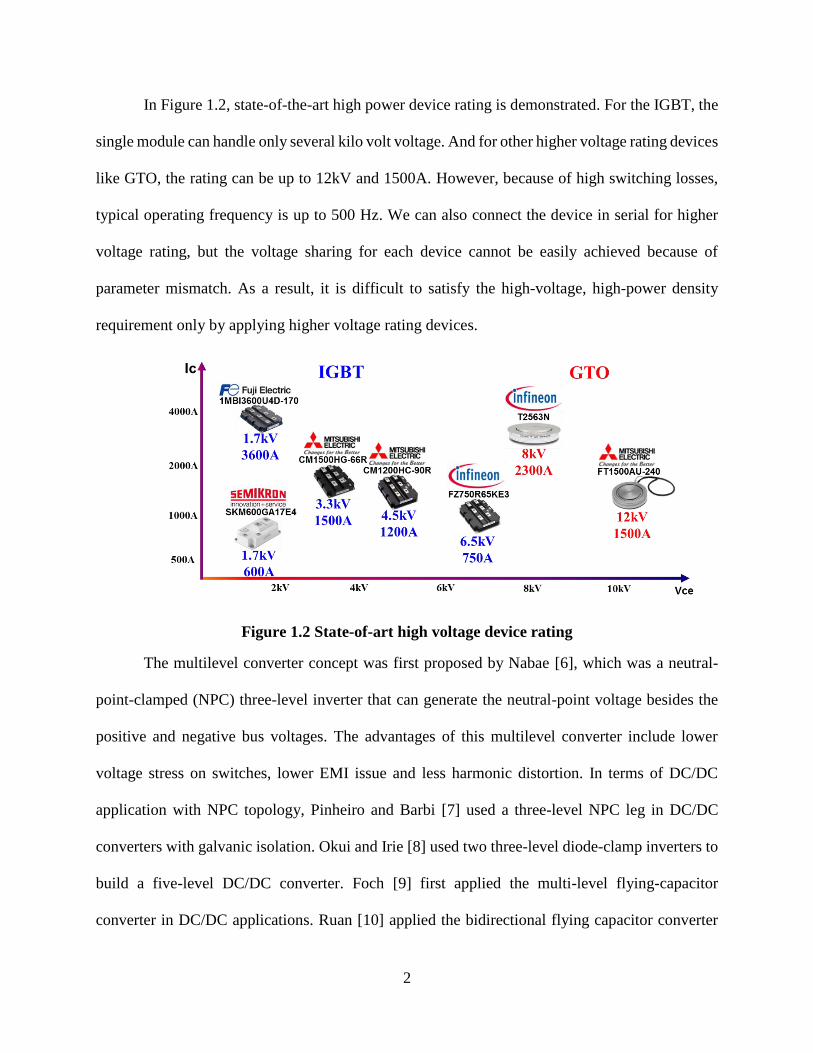
In Figure 1.2, state-of-the-art high power device rating is demonstrated. For the IGBT, the
single module can handle only several kilo volt voltage. And for other higher voltage rating devices
like GTO, the rating can be up to 12kV and 1500A. However, because of high switching losses,
typical operating frequency is up to 500 Hz. We can also connect the device in serial for higher
voltage rating, but the voltage sharing for each device cannot be easily achieved because of
parameter mismatch. As a result, it is difficult to satisfy the high-voltage, high-power density
requirement only by applying higher voltage rating devices.
Figure 1.2 State-of-art high voltage device rating
The multilevel converter concept was first proposed by Nabae [6], which was a neutral-
point-clamped (NPC) three-level inverter that can generate the neutral-point voltage besides the
positive and negative bus voltages. The advantages of this multilevel converter include lower
voltage stress on switches, lower EMI issue and less harmonic distortion. In terms of DC/DC
application with NPC topology, Pinheiro and Barbi [7] used a three-level NPC leg in DC/DC
converters with galvanic isolation. Okui and Irie [8] used two three-level diode-clamp inverters to
build a five-level DC/DC converter. Foch [9] first applied the multi-level flying-capacitor
converter in DC/DC applications. Ruan [10] applied the bidirectional flying capacitor converter

3
for the hybrid fuel cell power system where a bidirectional converter needs to be employed
between DC bus and battery to control the charge and discharge current. In terms of multi-level
buck/boost topology, Lee [11] mentioned the application of three-level boost converter for high
power and/or high voltage applications and the three-level bidirectional DC/DC converter can be
used in the renewable energy system where the power flow is bidirectional [12]. A generalized
multilevel converter topology is reported that can balance each dc voltage level automatically
without any assistance from other circuits [13]. Ruan [14][15] gives a systematic method to derive
a family of six non-isolated three-level DC/DC converters: buck, boost, buck-boost, Cuk, sepic
and zeta from the standard buck and boost converters.
The three-level NPC circuit can be extended to higher levels, thus a lower voltage stress
on semiconductor components and better harmonic performance [16][17]. [18] explored the
application of two back-to-back connected five-level diode-clamped converter legs. Fang Z. Peng
[19][20] used the four-level flying capacitor topology based DC/DC converter for PHEVs. The
inductance required can be largely reduced with a fixed duty cycle, thus power density can be
increased as well as the overall efficiency. Huang [21] applied five-level flying capacitor topology
for high-voltage, high-frequency DC/DC converter with solid state transformer. Barbi
[22][23][24][25] proposed the non-isolated five-level structure for buck-type, boost-type and the
bidirectional type suitable for high power applications. However, a large number of devices will
be needed and the system structure and control scheme will become more complex as the level
increases. Capacitor voltage balancing control will also become unattainable with higher levels.
The subject of multi-level converters has been widely pursued over the last three decades.
In principle, the concept can be extended to many levels for very high voltage applications.
However, due to the inherent complexity in topological structure, capacitor voltage balancing, and

4
associated controls, commercialization of the multilevel converters have been limited only to five
level to date.
1.2 Configuration of Multi-phase Three-level DC/DC Converter
In terms of non-isolated three-level DC/DC converter, there are two major suitable
candidates, flying-capacitor and three-level buck, which are shown in the Figure 1.3 and Figure
1.4, respectively. For flying-capacitor, there is 180 degree phase shift between switch S1 and S2,
and gate signals for S4 and S3 are complimentary to S1 and S2, respectively. For three-level buck,
the 180 degree phase shift is between switch S1 and S4.
Figure 1.3 Three-level flying-capacitor topology

5
Figure 1.4 Three-level buck topology
For these two types of topologies, the voltage polarity of both input and output sides are
fixed while the current can flow in both directions, such that the power can also flow bidirectional.
With the three-level structure, the inductor current ripple frequency will be twice the switching
frequency and size of passive components can be reduced. For capacitor voltage balance issue,
flying-capacitor needs to keep the voltage of flying cap at half of the dc link voltage Vdc [26]
while for three-level buck, neutral point voltage should be balanced. For flying-capacitor, it gives
common ground for input and output sides, but one more flying capacitor is required compared
with the three-level buck if considering the part number count. Based on these comparisons, the
three-level buck topology is chosen and analyzed in the rest of this paper for its simplicity and low
part number count.
For the power conversion system shown in the Figure 1.1, the AC/DC stage has been built
with three-level active neutral-point-clamped topology to achieve good performance and high
power density with 1200V/400A IGBT at the power rating of 200kW [27]. Taking safe margin of
the semiconductor device into consideration, a 1200V DC link is applied to connect AC/DC and
DC/DC stages. To have a modularized structure for the whole system, the same device is desired

6
to be employed for the DC/DC stage as AC/DC stage. Under the 200kW power rating, the lower
the voltage of DC application side, the more phase legs are needed to be paralleled at DC/DC stage
because of the higher possible RMS current. Assuming that the range of DC application side
voltage is 500V-800V, at least two paralleled three-level buck phase legs are needed to handle the
200kW power rating with enough safe margin considering 400A current rating.
Figure 1.5 gives the complete three-level power conversion system structure with 200kW
power rating with bidirectional power flow.
Figure 1.5 Three-level power conversion system
1.3 Objectives and Thesis Outline
With the configuration of the two-phase paralleled three-level DC/DC determined, this
paper focuses on the study to improve the power density and efficiency of the three-level DC/DC
conversion by addressing the magnetic design and integration process.
Chapter 1 provides the fundamental introduction for the two-stage three-level power
conversion system with its application for renewable energy systems. Possible topology candidates

7
for DC/DC conversion are compared and a two-phase three-level buck converter is applied as the
DC/DC conversion stage within the conversion system based on the power rating and performance
requirements. The conversion system aims at the power rating of 200kW, with bidirectional power
flow.
In chapter 2, non-interleaving and two types of interleaving methods are compared for the
paralleled three-level DC/DC converter. Interleaving operation can reduce the output current ripple,
but may cause significant inductor current ripple. This phenomenon is analyzed using equivalent
circuit of the converter. By applying the inverse coupling of two inductors, the circulating current
caused by interleaving can be suppressed. Three different scenarios for DC/DC converter,
including non-interleaving with non-coupling inductors, N-type interleaving with inversed
coupled inductors and Z-type interleaving with inversed coupled inductors, are analyzed carefully
in terms of current ripple and common-noise comparison.
Chapter 3 addresses the design issues concerning the inverse coupling of the two inductors
in two-phase interleaved three-level DC/DC converter. Because of the coupling of two inductors,
together with their associated switching networks, inductors act like nonlinear devices. It offers
additional benefits of containing the circulating current and minimizing total output current ripple.
This chapter presents the mathematical model for such coupled system and decouple it based on
the equivalent inductance concept. Design guidelines for coupling are provided according to
inductor current ripple and total output current ripple requirements.
Chapter 4 presents further improvement by integrating all the magnetics in a common
structure. An integrated coupled inductors structure was proposed, and it is hard to analyze the
coupling directly. Again, equivalent inductance analysis is applied, and can provide the guideline
for coupling design based on the current ripple target. The benefit of magnetic integration is

8
demonstrated by comparing with inverse coupling of two inductors. The concept of integrated
coupled inductors is verified with a prototype built with nano-crystalline magnetic material.
Hardware experiment results are demonstrated and discussed.
In the last chapter, the conclusion for the paper is summarized, emphasizing the benefit of
integrated coupled inductors with interleaved phase legs to push for high-power, high-performance
DC/DC conversion in renewable energy systems. Possible future work is introduced.
9
Chapter 2 Evaluation on Method of Interleaving for
Paralleled Three-level DC/DC Converter
As introduced in the previous chapter, two phase legs are employed for the DC/DC stage
considering the high-power, high-current rating requirements. This chapter will present an
overview of possible interleaving methods for the paralleled phase legs in the three-level DC/DC
converter, including non-interleaving, N-type interleaving and Z-type interleaving methods. The
comparison of different methods will be based on their effects on inductor current ripple and output
current ripple. An equivalent circuit is used to analyze the difference on ripple and give more
physical insight into why inverse coupled inductors can be beneficial with interleaving. In addition,
the common-mode voltage for all three cases are compared. The optimal interleaving method is
selected with trade-off between ripple reduction effect and common-mode voltage magnitude.
2.1 Interleaving Methods
2.1.1 In-phase Method
As for in-phase method [28], the two phase legs will have the same switching sequence
and there is no phase shift between the two legs. Figure 2.1 gives the circuit diagram and
corresponding waveforms. For both phase leg A and B, there will be 180 degree phase shift
between outer switches, S1a and S4a, or S1b and S4b. The corresponding inner switches, S2a and S3a,
or S2b and S3b, have the complementary gate signals with the outer switches to avoid shoot through
across the DC bus. Because of the non-interleaving method, two phase legs share the identical

10
output voltage and inductor current waveform. Clearly, this method is good for its simplicity.
However, since the output current is the summation of two inductor currents, the output current
ripple is large. Considering the possible scenario that the number of phase legs would increase as
the system power rating requirement increases, the output current ripple would become
unacceptable.
Figure 2.1 In-phase method
2.1.2 N-type Interleaving Method
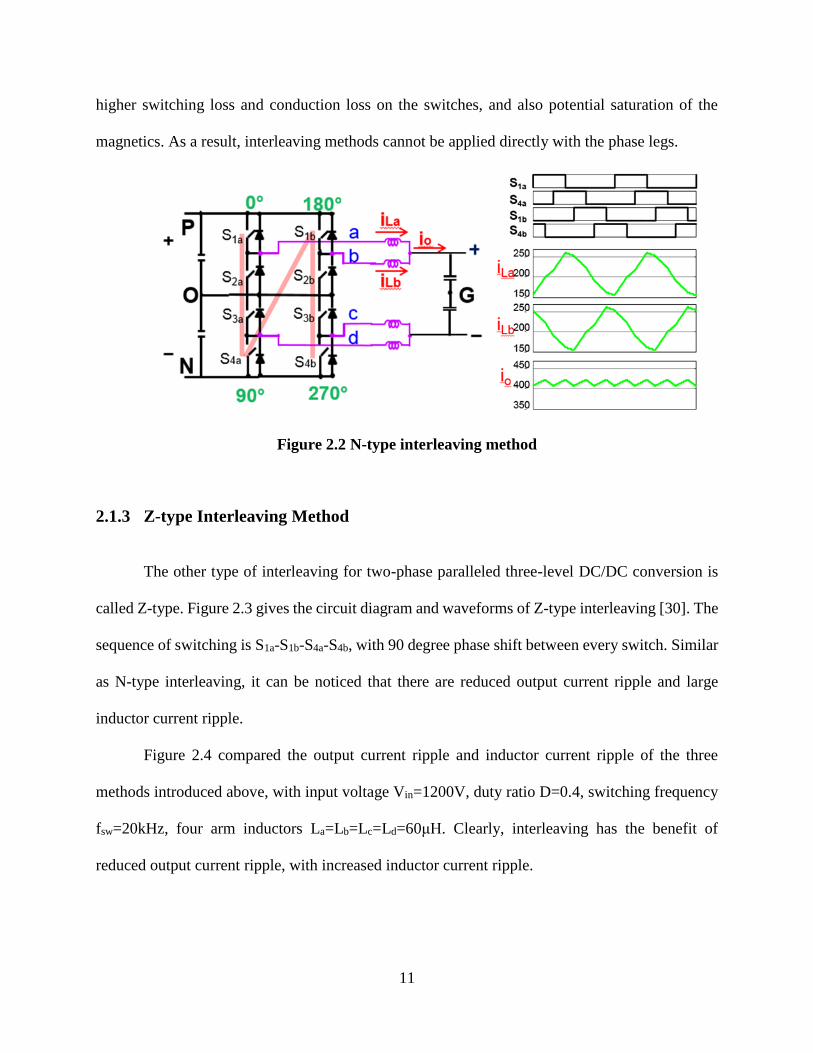
In comparison with non-interleaving, interleaving methods were introduced to reduce the
output current ripple. Figure 2.2 gives the circuit diagram and waveforms of N-type [29]. Since
the sequence of switching is S1a-S4a-S1b-S4b, there is 90 degree phase shift between every switch.
The name N-type comes from its switching sequence. Because of the ripple-cancelling effect, the
output current ripple can be reduced for both types of interleaving. However, it can be noticed
from the waveforms that inductor current ripple is huge, and causes problems including much
11
higher switching loss and conduction loss on the switches, and also potential saturation of the
magnetics. As a result, interleaving methods cannot be applied directly with the phase legs.
Figure 2.2 N-type interleaving method
2.1.3 Z-type Interleaving Method
The other type of interleaving for two-phase paralleled three-level DC/DC conversion is
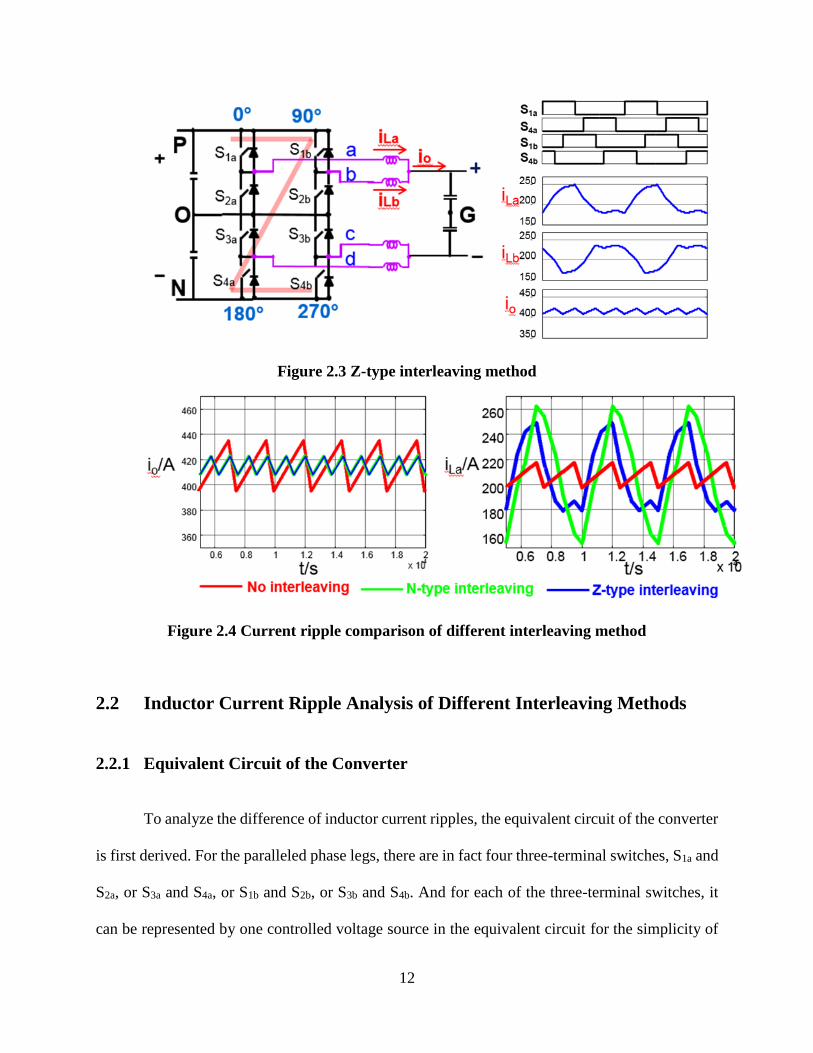
called Z-type. Figure 2.3 gives the circuit diagram and waveforms of Z-type interleaving [30]. The
sequence of switching is S1a-S1b-S4a-S4b, with 90 degree phase shift between every switch. Similar
as N-type interleaving, it can be noticed that there are reduced output current ripple and large
inductor current ripple.
Figure 2.4 compared the output current ripple and inductor current ripple of the three
methods introduced above, with input voltage Vin=1200V, duty ratio D=0.4, switching frequency
fsw=20kHz, four arm inductors La=Lb=Lc=Ld=60μH. Clearly, interleaving has the benefit of
reduced output current ripple, with increased inductor current ripple.
12
Figure 2.3 Z-type interleaving method
Figure 2.4 Current ripple comparison of different interleaving method
2.2 Inductor Current Ripple Analysis of Different Interleaving Methods
2.2.1 Equivalent Circuit of the Converter
To analyze the difference of inductor current ripples, the equivalent circuit of the converter
is first derived. For the paralleled phase legs, there are in fact four three-terminal switches, S1a and
S2a, or S3a and S4a, or S1b and S2b, or S3b and S4b. And for each of the three-terminal switches, it
can be represented by one controlled voltage source in the equivalent circuit for the simplicity of

13
analysis, namely vao, vbo, vco and vdo. As shown in the Figure 2.5, the inductor current iLa and iLb
can be decomposed by two parts. In detail, the inductor current iLa can be separated as common-
mode current icm and differential-mode current idm, and the relationship can be described as,
La cm dmi i i (2.1)
Similarly, the inductor current iLb can be seen as the difference between common-mode current icm
and differential-mode current idm.
Lb cm dmi i i (2.2)
Figure 2.5 Equivalent circuit of the converter
By superposition, one can divide the circuit into two parts, depending on the common-
mode and differential-mode current difference defined by (2.1) and (2.2) [30]. Figure 2.6 gives the
equivalent circuits for icm and idm. And together, these two circuits are equivalent to the upper part
of the circuit in Figure 2.5, as shown in the dashed square. Following this chapter, analysis will
focus on the equivalent circuit for the upper part of the circuit, and corresponding inductor current

14
iLa and iLb. The analysis process and result is similar for inductor current iLc and iLd in the lower
part of the circuit. For the simplicity of the content, it will not be discussed in detail.
Figure 2.6 Equivalent circuits for common-mode current and differential-mode current
In the equivalent circuit for common-mode current, only a common-mode voltage source
is included,
4 2
ao bo co do o
cm
v v v v vv
(2.3)
And it will generate the same common-mode current icm in inductor La and Lb. Since common-
mode current flows to the output side, it produces real power transfer from input to output.
In comparison, the differential-mode voltage source vdm will produce the differential-mode
current in the equivalent circuit. And generated idm is circulating between inductor La and Lb. As
a result, the differential-mode current idm can be viewed as a circulating current between the two
phase legs, and it should be avoided.
2
ao bo
dm
v vv
(2.4)

15
Figure 2.7 compares the common-mode current and differential-mode current among
different methods including non-interleaving, N-type interleaving and Z-type interleaving. And
the simulation condition for the waveform is, Vin=1200V, D=0.4, fsw=20kHz, La=Lb=Lc=Ld=60uH.
From the waveforms for common-mode voltage and current, one can conclude that due to the
difference of interleaving, the four controlled voltage sources vao, vbo, vco and vdo in Figure 2.5 will
have different voltage sequences, thus causing the difference in common-mode voltage vcm
according to (2.3). For non-interleaving, the magnitude of the vcm is large and the frequency is
twice the switching frequency. For both N-type and Z-type interleaving, the magnitudes of the vcm
are identical and relatively small compared with non-interleaving case. Also the frequency of vcm
is four times the switching frequency. Accordingly, the current ripple icm is smaller in both N-type
and Z-type interleaving compared with non-interleaving case.
Figure 2.7 Common-mode current and differential-mode current comparison

16
In terms of differential-mode voltage and current, the two phase legs have identical
switching sequences for non-interleaving and vdm will remain zero by (2.4). Since no differential-
mode current exists in the non-interleaving case, only current ripple of icm will contribute to the
inductor current ripple. In contrast, because of the interleaving, both N-type and Z-type
interleaving will have differential-mode voltage with large magnitude, causing huge differential-
mode current ripple, as illustrated in the bottom line of the Figure 2.7. Due to this huge circulating
current between the two phase legs, the current ripple on the inductors is not acceptable.
2.2.2 Inductor Current Ripple Reduction by Inverse Coupled Inductors
To suppress the huge inductor current ripple caused by interleaving, the method of applying
inverse coupled inductors with the converter was proposed [30]. Figure 2.8 shows the converter
with the inverse coupled inductors and two coupled inductors are needed for the two phase legs.
For example, the inverse coupling between Laa and Lbb is used to suppress the circulating current
between them.
Figure 2.8 Applying inverse coupled inductors with the converter

17
Figure 2.9 Equivalent circuit for differential-mode current with coupled inductors
Following the analysis method in 2.2.1, one can also give the equivalent circuit for the
differential-mode current with coupled inductors, as shown in Figure 2.9. Because of the inverse
coupling, the differential-mode current sees high impedance in the equivalent circuit, and the
differential-mode current ripple will become small.
Figure 2.10 Differential-mode current ripple reduction for N-type interleaving

18
Based on the simulated waveforms in Figure 2.10, for N-type interleaving, the differential-
mode current decreases largely by applying inverse coupled inductors. Since the contribution of
differential-mode current ripple to the inductor current ripple drops, the overall inductor current
ripple drops accordingly by applying the coupled inductors instead of single inductors. The same
conclusion can be drawn for Z-type interleaving, as shown in Figure 2.11. The inductor current
ripple drops as the differential-mode current ripple is suppressed by inverse coupling.
Figure 2.11 Differential-mode current ripple reduction for Z-type interleaving

19
Figure 2.12 Inductor current ripple reduction with inverse coupling
The simulation result in Figure 2.12 verifies the effect of applying inverse coupled
inductors, with duty cycle D=0.4. With inverse coupling, either N-type interleaving or Z-type
interleaving can reduce the inductor current ripple dramatically compared with applying non-
coupling inductors.
2.3 Common-mode Voltage Analysis of Different Interleaving Methods
Although both N-type and Z-type interleaving have the inductor current ripple reduction
effect, there will be differences from other important aspects, including the common-mode voltage
in terms of the common-mode noise issue of the converter. Figure 2.13 defines the common-mode
voltage vGO of the converter,
4
ao bo co do
GO
v v v vv
(2.5)

20
Figure 2.13 Common-mode voltage of the converter
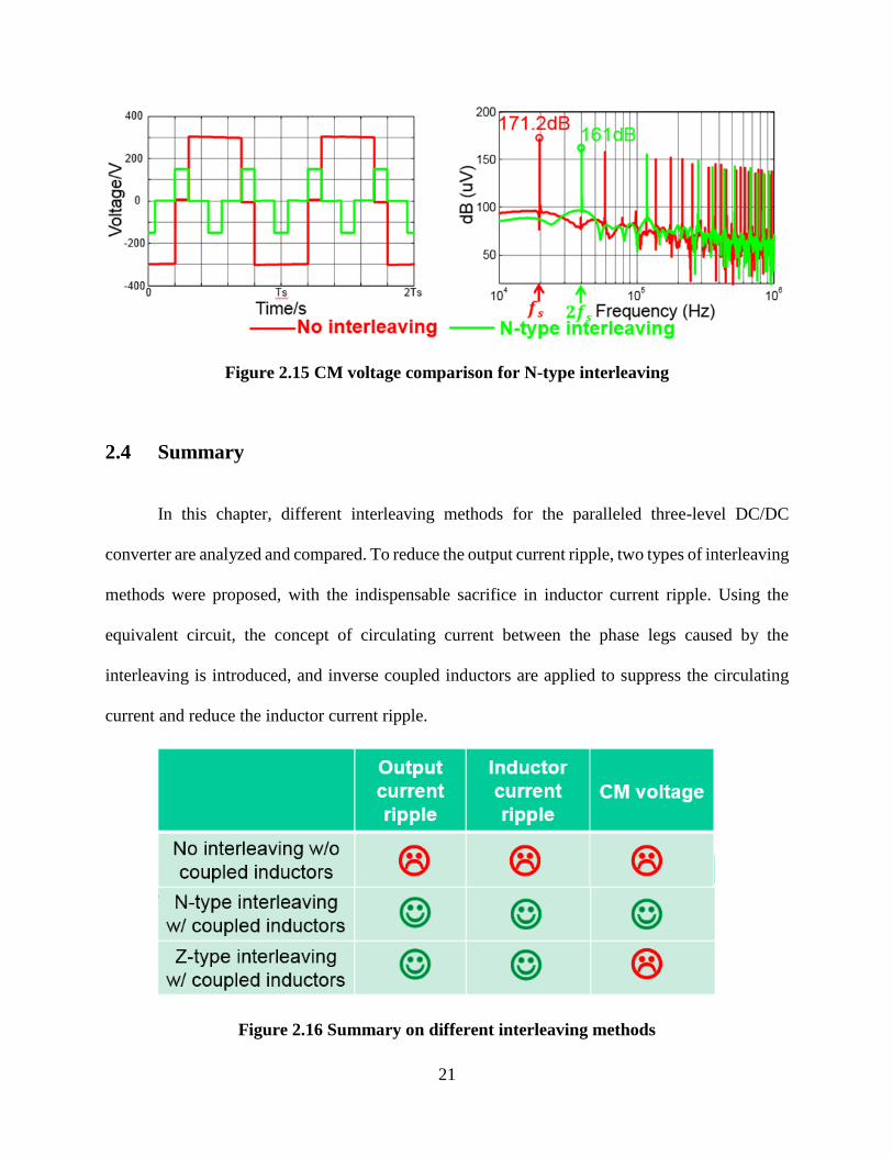
As shown in the Figure 2.14 and Figure 2.15, the common-mode voltage of Z-type
interleaving has the first peak at switching frequency in the spectrum, which is the same as the
non-interleaving case. Also, the magnitude of the first peak is about the same as non-interleaving.
In contrast, the first peak of N-type interleaving is at twice the frequency, with the magnitude
reduced to 161dB. As a result, N-type interleaving is much better than the Z-type interleaving for
the common-mode noise filter design.
Figure 2.14 CM voltage comparison for Z-type interleaving
21
Figure 2.15 CM voltage comparison for N-type interleaving
2.4 Summary
In this chapter, different interleaving methods for the paralleled three-level DC/DC
converter are analyzed and compared. To reduce the output current ripple, two types of interleaving
methods were proposed, with the indispensable sacrifice in inductor current ripple. Using the
equivalent circuit, the concept of circulating current between the phase legs caused by the
interleaving is introduced, and inverse coupled inductors are applied to suppress the circulating
current and reduce the inductor current ripple.
Figure 2.16 Summary on different interleaving methods

22
Three possible operating methods are listed in Figure 2.16, including non-interleaving with
single inductors, N-type interleaving with inverse coupled inductors, and Z-type interleaving with
inverse coupled inductors. The conventional non-interleaving serves as the benchmark, and both
N-type and Z-type interleaving with inverse coupled inductors have much smaller output current
ripple and inductor current ripple. For the benefit of the common-mode noise filter, N-type
interleaving is more advantageous than the Z-type interleaving. In summary, N-type interleaving
with inverse coupled inductors is the optimal configuration for the performance of two-phase
three-level DC/DC converter.

23
Chapter 3 Modeling and Design of Inductor Inverse
Coupling
Two coupled inductors are used in the three-level DC/DC converter to reduce the inductor
current ripple, and this chapter will study in detail the effect of coupling for the steady-state
operation of the converter. The coupling effect makes the inductors become non-linear, and
different equivalent inductance shows up in one switching cycle. By using the concept of
equivalent inductance, the coupled inductors can be decoupled in math and can easily be compared
with the non-coupling inductor case. In this way, the relationship between coupling and both
inductor current ripple and output current ripple will be built, and the benefit of coupling can be
illustrated clearly. The coupled inductors can be designed based on the inductor current ripple and
output current ripple requirements following the design procedure provided.
3.1 Review on the Concept of Non-linear Equivalent Inductance
The concept of non-linear equivalent inductance was first introduced by Pit-Leong Wong
[31], analyzing the effect of coupled inductors to improve transient response and reduce steady-
state ripple in the multi-phase interleaving buck VRM. Section 3.1 will give a brief introduction
to the non-linear equivalent inductance in multi-phase buck. And the same analysis method using
the equivalent inductance concept will be adopted in the following section for the case of two-
phase three-level DC/DC converter with coupled inductors.

24
Figure 3.1 Interleaving bucks with coupled inductors
As shown in Figure 3.1, coupled inductors are used in interleaving bucks and the
corresponding inductor voltage waveform is drawn in Figure 3.2. In one switching cycle, there are
four different inductor voltage conditions.
Figure 3.2 Inductor voltage waveform for interleaving buck
In addition, from Figure 3.3, the non-linearity of the inductors can be observed. To analyze
the coupling effect for inductor current, Wong used the concept of equivalent inductance to
mathematically decouple the coupled inductors. Overall, there are three different equivalent
inductances in one switching cycle and can be defined and derived from the circuit analysis,

25
2
1
1'
eq
ML
LLM D
L D
(3.1)
2 eqL L M (3.2)
2
3 '1
eq
ML
LLM D
L D
(3.3)
Figure 3.3 Inductor current waveform with coupled inductors
The case with duty cycle larger than 0.5 can be analyzed in a similar way.
By applying the concept of equivalent inductance, the coupled inductors are decoupled.
Therefore, the inductor ripple and output current ripple can be derived easily with equivalent
inductance by every time interval in one switching period. At the same time, the effect of coupling
can be clarified by comparing with non-coupling inductor case. In Figure 3.3, inductor current

26
with coupled inductors is plotted in the solid line, and inductor current with non-coupling inductors
is shown in the dashed line. Clearly, the first time interval determines the inductor current ripple,
1
a swcp
eq
v DTi
L (3.4)
With Leq1>L, the inductor current ripple can be smaller by coupling. Leq1 is defined as steady-state
equivalent inductance Lss for it determines the steady-state inductor current ripple.
It could also be found that Leq2 determines the transient response of the converter. Therefore,
Leq2 is defined as transient equivalent inductance Ltr.
From the equivalent inductance derivation from the inductor equation and waveform
analysis above, one can conclude that the concept of equivalent inductance is a helpful tool to
illustrate the benefit of coupled inductors in interleaving buck. Proper design of coupling can
improve steady-state performance and transient response speed. Also, it should be pointed out that
the concept of equivalent inductance is not purely mathematical, it also has strong physical
meaning [31].
3.2 Equivalent Inductance for Coupled Inductors with N-type Interleaving
The concept of equivalent inductance can be extended to the two-phase three-level DC/DC
converter with coupled inductors. Due to the N-type interleaving and three-level structure, there
will be differences in the equivalent inductance derivation. By giving the equivalent inductance,
the coupling effect on converter performance can then be discussed in the next section.

27
Figure 3.4 Three-level DC/DC converter with coupled inductors
There are two coupled inductors in the two-phase three-level DC/DC converter, as shown
in Figure 3.4. Figure 3.5 gives the flux distribution for the coupled inductors on arm a and arm b.
For the flux generated by winding of Laa, part of flux goes through arm b and part goes through
the center leg, namely Φba and Φlka. The flux generated by winding of Lbb has a similar flux path,
namely Φab and Φlkb. Green lines represent the inverse coupled flux between two arms, and there
is leakage flux, Φlka and Φlkb, flows through the center leg, as shown in the purple dashed lines.
Figure 3.5 Flux analysis of coupled inductors
28
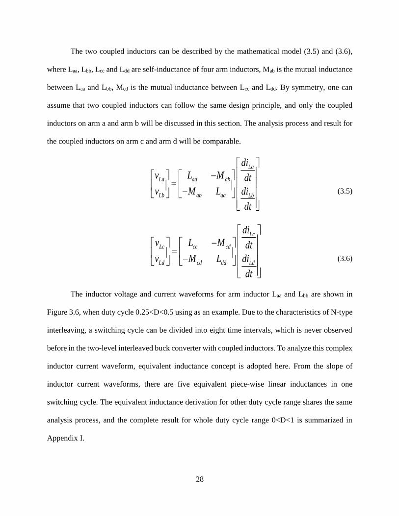
The two coupled inductors can be described by the mathematical model (3.5) and (3.6),
where Laa, Lbb, Lcc and Ldd are self-inductance of four arm inductors, Mab is the mutual inductance
between Laa and Lbb, Mcd is the mutual inductance between Lcc and Ldd. By symmetry, one can
assume that two coupled inductors can follow the same design principle, and only the coupled
inductors on arm a and arm b will be discussed in this section. The analysis process and result for
the coupled inductors on arm c and arm d will be comparable.
La
La aa ab
Lb ab aa Lb
di
v L M dt
v M L di
dt
(3.5)
Lc
Lc cc cd
Ld cd dd Ld
di
v L M dt
v M L di
dt
(3.6)
The inductor voltage and current waveforms for arm inductor Laa and Lbb are shown in
Figure 3.6, when duty cycle 0.25<D<0.5 using as an example. Due to the characteristics of N-type
interleaving, a switching cycle can be divided into eight time intervals, which is never observed
before in the two-level interleaved buck converter with coupled inductors. To analyze this complex
inductor current waveform, equivalent inductance concept is adopted here. From the slope of
inductor current waveforms, there are five equivalent piece-wise linear inductances in one
switching cycle. The equivalent inductance derivation for other duty cycle range shares the same
analysis process, and the complete result for whole duty cycle range 0<D<1 is summarized in
Appendix I.

29
Figure 3.6 Inductor voltage and current waveforms for N-type interleaving
For the simplicity of analysis, the self-inductance of two inductors, Laa and Lbb, are
assumed to be identical, with
aa bbL L L (3.7)
The mutual inductance Mab is defined as,
, ( 1 0) abM L (3.8)

30
As a result, the relationship of inductor voltage and current can be simplified by the 2x2
matrix below,
La
La ab
Lb ab Lb
di
v L M dt
v M L di
dt
(3.9)
And it can be rewritten without assumption as,
2
2
0
0
Laab abLa Lb
ab LbabLb La
diM Mv v L
dtL L
M diMv v L
L dtL
(3.10)
Clearly, the right side of the equation is decoupled already. If the relationship between two
inductor voltages vLa and vLb can be found, the coupled inductors can be decoupled mathematically.
Figure 3.7 Equivalent circuit with coupled inductors
From the circuit diagram, or equivalent circuit of the converter with coupled inductors in
Figure 3.7, the inductor voltage is,
31
2
2
oLa ao GO
oLb bo GO
Vv v v
Vv v v
(3.11)
With vGO is derived from the equivalent circuit and can be defined as,
4
ao bo co do
GO
v v v vv
(3.12)
Using the first time interval t0-t1 in Figure 3.8 as an example to derive the equivalent
inductance. For the there-level DC/DC converter, there exists,
in oDV V (3.13)
Where Vin is the input voltage, and Vo is the output voltage. Also,
04
ao bo co do
GO
v v v vv
(3.14)
(1 )
2 2
o in
La ao GO
V D Vv v v
(3.15)
2 2 o in
Lb bo GO
V DVv v v
(3.16)
The relationship for two inductor voltages can be found as,
1
Lb La
Dv v
D (3.17)
With this relationship, (3.10) becomes,

32
2 2
2 2
( )0
1
( )0
1
ab
La
abLa
Lb Lbab
ab
L M
diDL M
v dtD
v diL M
D dtL M
D
(3.18)
By the mathematical process using inductor voltage relationship, now coupled inductors
are decoupled in the inductor equation, and one can define the equivalent inductance in this time
interval in terms of arm a,
2 2
1
( )
1
abeq
ab
L ML
DL M
D
(3.19)
For the equivalent inductance on arm b, it will be identical as arm a with only a difference of 180
degree phase shift due to the N-type interleaving.
Also notice that Leq1 in the three-level converter is the same as the Leq1 in two-level buck
converter case in section 3.1. In time interval t2-t3, the two inductor voltages are identical as in
time interval t0-t1, accordingly the equivalent inductance in this interval is still Leq1.
Different inductor voltage combinations are shown with different color in Figure 3.8. For
other time intervals, once the relationship of two inductor voltages are found, the corresponding
equivalent inductance can be derived together with (3.18).

33
Figure 3.8 Five different equivalent inductance in three-level converter
For time interval t3-t4 and t7-t8 in the red shaded area in Figure 3.8,
(1 4 )
8
in
La
D Vv
(3.20)
(1 4 )
8
in
Lb
D Vv
(3.21)
2 eq abL L M (3.22)
For time interval t4-t5 and t6-t7 in the green shaded area in Figure 3.8,
2
in
La
DVv
(3.23)

34
(1 )
2
in
Lb
D Vv
(3.24)
2 2
3
( )
1
abeq
ab
L ML
DL M
D
(3.25)
For time interval t1-t2 in the pink shaded area in Figure 3.8,
(3 4 )
8
in
La
D Vv
(3.26)
(1 4 )
8
in
Lb
D Vv
(3.27)
2 2
4
( )
(1 4 )
(3 4 )
abeq
ab
L ML
DL M
D
(3.28)
For the last remaining time interval t5-t6 in the yellow shaded area in Figure 3.8,
(1 4 )
8
in
La
D Vv
(3.29)
(3 4 )
8
in
Lb
D Vv
(3.30)
2 2
5
( )
(3 4 )
(1 4 )
abeq
ab
L ML
DL M
D
(3.31)

35
Totally, there are five different inductor voltage combinations. As a result, five different equivalent
inductances exist within one switching period.
Among the five equivalent inductances, Leq1, Leq2 and Leq3 showed up in section 3.1 for the
interleaving buck converter case, and Leq4, Leq5 are two new equivalent inductances that uniquely
exist in the three-level interleaving with coupled inductors case.
3.3 Coupling Effect on Inductor Current Ripple and Output Current Ripple
Figure 3.9 provides the waveform of inductor current with coupled inductors, as shown in
the red solid lines. And the inductor current with non-coupling inductors for the three-level DC/DC
converter in the dashed lines is set as the benchmark. Comparing with the inductor current
waveform in interleaving buck converter, now inductor current ripple is not determined solely by
one equivalent inductance in the three-level case. Instead, the first three time intervals determine
the inductor current ripple together.
1 2 3La La LaT T Tnc
v v vi
L
(3.32)
31 2
1 4 1
LaLa La TT Tcp
eq eq eq
vv vi
L L L
(3.33)
Where nci is inductor current ripple with non-coupling inductors and cpi is for the coupled
inductors case.

36
Figure 3.9 Inductor current waveform with coupled inductors in three-level DC/DC
converter, 0.25<D<0.5
Considering the case 0.25<D<0.5, due to the special characteristics of inductor current
ripple determination, it is hard to compare the inductor current ripple between the coupled
inductors case and the non-coupling case by comparing equivalent inductance with non-coupling
inductance L. To solve this problem, the steady-state equivalent inductance in the three-level
DC/DC converter is defined as,
1 2 3 1 2 3
31 2
1 4 1
La La La La La LaT T T T T Tss
LaLa Lacp TT T
eq eq eq
v v v v v vL
vv vi
L L L
(3.34)
With simple mathematical derivation, (3.34) becomes,

37
2 2 2
2 2
( 8 10 1)( )
( 8 10 1) (8 2 1)
abss
ab
D D L ML
D D L D D M (3.35)
And now Lss can be compared with non-coupling inductance L to find the inductor current ripple
reduction effect with coupled inductors.
Under the condition that,
2
2
8 2 1
8 10 1
abM D D
L D D (3.36)
Steady-state equivalent inductance Lss will be larger than the non-coupling inductance L. And the
inductor current ripple can be reduced with coupled inductors with proper coupling coefficient.
Besides inductor current ripple, output current ripple is another important design
specifications need to be considered. As shown in Figure 3.10, the output current waveform io is
the summation of two inductor currents, iLa and iLb. In the time interval t3-t4, the output current
ripple is derived as the summation of two inductor current ripples,
4 4
2 2
La LbT To
eq eq
v vi
L L
(3.37)
Clearly, equivalent inductance Leq2 determines the output current ripple. And the same conclusion
can be drawn for all other duty cycle cases.
Another way to find out the output current ripple determination is to add the two equations
in (3.9) together, and,
2
( )( )
La Lb o
La Lb ab eq
d i i div v L M L
dt dt (3.38)

38
Figure 3.10 Output current waveform with coupled inductors in three-level DC/DC
converter
Since voltage on inductors are decided by the operation condition of the converter, one can
conclude that Leq2 determines the output current waveform. Noted that,
2eq ab lkL L M L (3.39)
And Leq2, or the leakage inductance Llk in fact determines the output current ripple.
Up to this point, the relationship between the equivalent inductance and current ripple with
coupled inductors is found. However, to better illustrate the benefit of applying coupled inductors,

39
converter with non-coupling inductor case should be adopted as the benchmark. To have a fair
comparison, the same output current ripple is set as the condition for comparison. Under this
scenario, Leq2 in coupled inductors case should be equal to non-coupling inductance,
2nc eqL L (3.40)
Where Lnc is the non-coupling inductance.
Under the condition (3.40), the ratio of inductor current ripples between coupling and non-
coupling case is,
2 2
2
( 8 10 1) (8 2 1),0.25 0.5
( 8 10 1)(1 )
cp nc
nc ss
i L D D D DD
i L D D
(3.41)
With duty cycle ranges from 0.25 to 0.5. Other duty cycle cases can be defined with same
comparison method.
( 4 3) (4 1),0 0.25
(4 3)( 1)
cp nc
nc ss
i L D DD
i L D (3.42)
2 2
2
( 8 6 1) (8 14 7),0.5 0.75
( 8 6 1)(1 )
cp nc
nc ss
i L D D D DD
i L D D (3.43)
(4 1) ( 4 5),0.75 1
(4 1)(1 )
cp nc
nc ss
i L D DD
i L D (3.44)
Based on (3.41)-(3.44), the inductor current ripple reduction effect with different coupling
coefficient and duty cycle can be demonstrated clearly in Figure 3.11.

40
Figure 3.11 Inductor current ripple reduction with changing coupling coefficient and duty
ratio
At any duty cycle, the inductor current ripple reduction effect will be stronger as the
coupling effect of coupled inductors increases. And it should be noted that the comparison is based
on keeping same Leq2 as Lnc to guarantee a same output current ripple. Strong coupling is preferred
for inductor current ripple reduction while keeping same Leq2.
In order to see the effect of duty cycle on inductor current ripple reduction, the 3-D plot in
Figure 3.11 can be rotated into Figure 3.12. From the figure, when the coupling coefficient is fixed,
there are three maximum reduction effect points at D=0.25, D=0.5 and D=0.75. In other words,
given a coupled inductors design, it has the minimum inductor current ripple when operating at
D=0.25, D=0.5 and D=0.75.

41
Figure 3.12 Inductor current ripple reduction with changing coupling coefficient and duty
ratio, from different view
3.4 Coupling Design based on Current Ripple Requirement
For the inverse coupled inductors, two parameters in the (3.9) should be designed based on
the current ripple requirement, the mutual inductance Mab and the leakage inductance Llk. The self-
inductance equals to L=Mab+Llk.
In section 3.3, it can be concluded that equivalent inductance Leq2 will determine the output
current ripple of three-level DC/DC converter with coupled inductors, and multiple equivalent
inductances will affect the inductor current ripple. By calculating the relationship between
equivalent inductance and the current ripple,

42
2
2
2
2
(1 4 )0.25
4
(4 1)(1 2 ) 0.25 0.5
8
(3 4 )(2 1) 0.5 0.75
8
(4 3)(1 ) 0.75 1
4
dc
dc
eq
e
o
d
q
eq
eq
c
dc
V DDT D
V DD T D
iV D
D T D
V DD
L
L
T D
L
L
(3.45)
(1 4 )0.25
8 4
(4 1)(1 2 ) 0.25 0.5
16 4
(3 4 ) (1 )(2 1) 0.5 0.75
1
(2 )
(2 )
(26 4
(4 3) (1 )(1 ) 0.75
8 4
)
(2 )
lk ab lk
lk ab lk
l
dc dc
dc dc
La
dc dc
d
k ab lk
lk ab l
d
k
c c
V D V DDT T D
V D V DD T T D
iV D V D
D T T D
V D V DD T T D
L M L
L M L
L M L
L M L
(3.46)
Clearly, only Leq2 (=Llk) will affect the output current ripple, while both Mab and Llk will
affect inductor current ripple. As a result, the design process can be summarized as two steps. First,
the leakage inductance Llk should be designed based on the output current ripple requirement. With
Llk determined, the mutual inductance Mab then will be designed based on the inductor current
ripple requirement.
As the first step, Leq2 should be designed based on the output current ripple. With different
Leq2 value, the output current ripple varies in the whole duty cycle range from 0 to 1, as shown in
Figure 3.13. Input voltage Vdc=1200V, switching frequency fsw=20kHz. As the value of Leq2
43
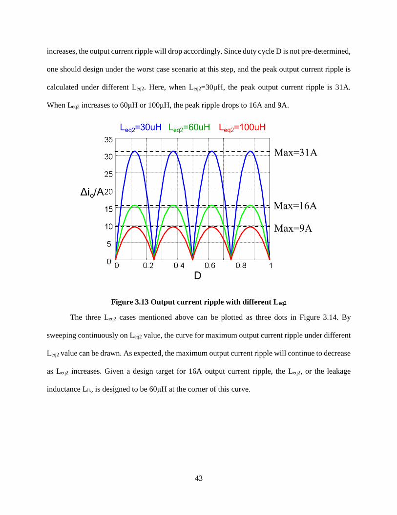
increases, the output current ripple will drop accordingly. Since duty cycle D is not pre-determined,
one should design under the worst case scenario at this step, and the peak output current ripple is
calculated under different Leq2. Here, when Leq2=30μH, the peak output current ripple is 31A.
When Leq2 increases to 60μH or 100μH, the peak ripple drops to 16A and 9A.
Figure 3.13 Output current ripple with different Leq2
The three Leq2 cases mentioned above can be plotted as three dots in Figure 3.14. By
sweeping continuously on Leq2 value, the curve for maximum output current ripple under different
Leq2 value can be drawn. As expected, the maximum output current ripple will continue to decrease
as Leq2 increases. Given a design target for 16A output current ripple, the Leq2, or the leakage
inductance Llk, is designed to be 60μH at the corner of this curve.

44
Figure 3.14 Design Leq2 based on output current ripple
In the second step, the mutual inductance Mab will be designed based on inductor current
ripple. With Llk=60μH, the inductor current ripple is calculated with different mutual inductance.
With Mab=200μH, 500μH and 800μH, the peak inductor current ripple is calculated as 21A, 13A,
and 11A, respectively in Figure 3.15.
By sweeping the maximum inductor current ripple with different Mab value, Figure 3.16 is
drawn. As Mab increases, the maximum inductor current ripple drops, while the benefit will
continue to diminish. Again, Mab value should be designed on the corner of the curve to have the
best trade-off. Given the inductor current ripple requirement as 13A, the mutual inductance Mab is
designed as 500μH.

45
Figure 3.15 Inductor current ripple with different Mab
Figure 3.16 Design Mab based on inductor current ripple

46
Figure 3.17 Inductor current ripple comparison
With the two steps above, mutual inductance Mab is design as 500μH and leakage
inductance Llk is designed as 60μH for the inverse coupled inductors. Under this condition, the
effect of inductor current ripple reduction is compared to the case of non-interleaving with single
inductors (L=60μH) in Figure 3.17. For most of the duty cycle ranges, the inductor current ripple
is largely reduced.
3.5 Magnetic Circuit Analysis
From the analysis from the previous section, it is important to have strong coupling for the
coupled inductors for inductor current ripple reduction. And this section will discuss the method
to provide strong coupling for proper air gap design. In the magnetic circuit shown in Figure 3.18,
the reluctance of the magnetic path is represented by the resistor and the winding is represented by
the magnetomotive force (MMF) source, which has similar characteristics of voltage source in

47
electric circuits. Assuming that the reluctance of the air gap is much larger than the reluctance of
the core, only air gap reluctance is considered in the magnetic circuit [32].
Figure 3.18 Magnetic circuit of coupled inductors
For the case where the cross section area for outer leg is A and 2A for the center leg, the
corresponding reluctance are,
11
o
lR
A (3.47)
22
2
o
lR
A (3.48)
Where l1 is the length of air gap in outer legs, l2 is the length of air gap in center leg.
As mentioned in the previous section, since Leq2=L-Mab=Llk determines the output current
ripple, one can keep the leakage inductance constant and then design proper air gap to achieve
strong coupling. From the magnetic circuit,
22
02
2 1 1 22
eq lk
N ANL L
R R l l (3.49)
48
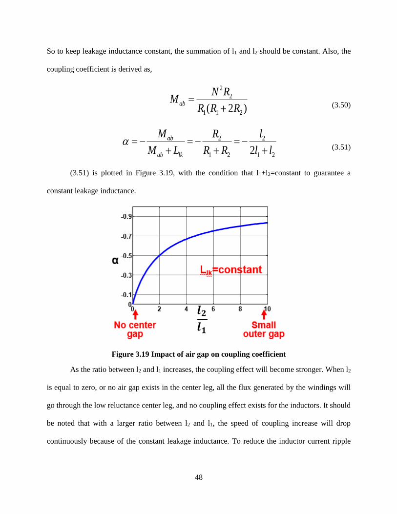
So to keep leakage inductance constant, the summation of l1 and l2 should be constant. Also, the
coupling coefficient is derived as,
2
2
1 1 2( 2 )
ab
N RM
R R R (3.50)
2 2
1 2 1 22
ab
ab lk
M R l
M L R R l l (3.51)
(3.51) is plotted in Figure 3.19, with the condition that l1+l2=constant to guarantee a
constant leakage inductance.
Figure 3.19 Impact of air gap on coupling coefficient
As the ratio between l2 and l1 increases, the coupling effect will become stronger. When l2
is equal to zero, or no air gap exists in the center leg, all the flux generated by the windings will
go through the low reluctance center leg, and no coupling effect exists for the inductors. It should
be noted that with a larger ratio between l2 and l1, the speed of coupling increase will drop
continuously because of the constant leakage inductance. To reduce the inductor current ripple

49
while keeping output current ripple controlled, strong coupling is preferred by increasing the center
air gap or reducing the outer air gap, while keeping the summed length of two air gaps constant.
3.6 Summary
This chapter is aiming at using the equivalent inductance concept to analyze the effect of
coupled inductors in the steady-state performance of three-level DC/DC converter, and to provide
guidance for coupling design.
With the equivalent inductance analysis for interleaving buck as a reference, the same
method is applied to derive the equivalent inductance in three-level DC/DC converter. The
connection between equivalent inductance and both inductor current ripple and output current
ripple is built. For inductor current ripple, it is not determined by one equivalent inductance, and
a new steady-state equivalent inductance is derived for its determination. For output current ripple,
it is decided by the Leq2, or the leakage inductance Llk of the coupled inductors.
To design the coupled inductors, a two-step procedure is provided based on the current
ripple requirements. The leakage inductance Llk is designed based on the maximum output current
ripple requirement, and then mutual inductance Mab will be designed based on the maximum
inductor current ripple requirement.
To have a fair comparison between coupling and non-coupling inductors, the same output
current ripple is assumed and Leq2 of coupled inductors is equal to the non-coupling inductance
Lnc. Under this condition, it is discovered that strong coupling is desired for inductor current ripple
reduction. And by analyzing the magnetic circuit, the strong coupling can be designed by
controlling the air gaps in the magnetic core, and both small inductor current ripple and output
current ripple can be achieved.

50
Chapter 4 Magnetic Integration for Coupled Inductors
Coupled inductors are required for interleaving three-level DC/DC converter to have small
inductor current ripple and output current ripple, as stated in chapter 3. The coupling can be
designed based on the current ripple requirement with equivalent inductance analysis. In this
chapter, a new type of integrated coupled inductors [33] is introduced to further reduce the size of
the magnetics and improve the power density of the converter. Two types of coupling effects, both
negative coupling to suppress the circulating current and positive coupling to increase output filter
inductance, exist in the integrated coupled inductors. The coupling effect on the current ripple
reduction will be discussed based on the equivalent inductance analysis, the same method as is
applied in chapter 3. With equivalent inductance defined, the relationship between current ripple
and coupling effect can be found, and design procedure for coupling will be given. A prototype of
integrated coupled inductors is built with nano-crystalline material, and is verified and tested with
the three-level DC/DC converter hardware.
4.1 Introduction on Concept of Integrated Coupled Inductors
Coupled inductors in three-level DC/DC converter is crucial to improve steady-steady
performance with interleaving. Due the requirement of the converter, two coupled inductors are
required. Laa and Lbb are inverse coupled, and Lcc and Ldd are inverse coupled, as shown in the
Figure 3.4. The core structure is shown in the Figure 4.1, and two sets of E-E core are needed.
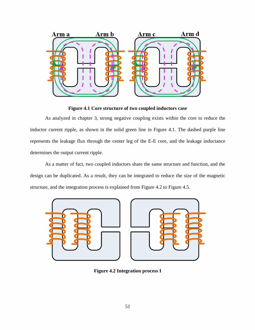
51
Figure 4.1 Core structure of two coupled inductors case
As analyzed in chapter 3, strong negative coupling exists within the core to reduce the
inductor current ripple, as shown in the solid green line in Figure 4.1. The dashed purple line
represents the leakage flux through the center leg of the E-E core, and the leakage inductance
determines the output current ripple.
As a matter of fact, two coupled inductors share the same structure and function, and the
design can be duplicated. As a result, they can be integrated to reduce the size of the magnetic
structure, and the integration process is explained from Figure 4.2 to Figure 4.5.
Figure 4.2 Integration process I

52
Figure 4.3 Integration process II
As shown in Figure 4.1, the center leg provides the path for leakage flux. It can be moved
to the outer side, as shown in Figure 4.2, and this new structure will not affect the coupling effect.
Since two coupled inductors are required for the converter, the two center legs can be moved to
the outer side and combined as one, as shown in the Figure 4.3 as the second step of integration.
Under this condition, the leakage flux from winding a & b, and the leakage flux generated by
winding c & d, will share the same path in the new center leg. At the same time, it should be noted
that the leakage flux represented by the purple dashed line is positively coupled through the low
reluctance path of core magnetic material. As a result, it is easy to form the idea of removing the
center leg and letting all previous leakage flux positively couple together, as shown in Figure 4.4.
Now two types of coupling exist in the integrated coupled inductors, including negative
coupling represented by the solid green line to reduce the circulating current in arm a-b or c-d, and
the positive coupling represented by the dashed purple line to increase the output inductance. The
inductor equation now becomes a 4x4 matrix,
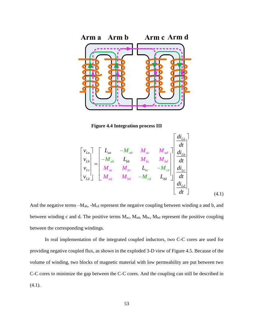
53
Figure 4.4 Integration process III
La
La aa abLb
Lb bb
Lc
ac ad
bc b
cc L
ab
cd
cd
c
Ld dd
L
d
ac bc
ad
d
bd
M M
M M
M M
M M
di
dtv L di
v L dt
v L di
dtv L
di
d
M
M
M
t
M
(4.1)
And the negative terms –Mab, -Mcd represent the negative coupling between winding a and b, and
between winding c and d. The positive terms Mac, Mad, Mbc, Mbd represent the positive coupling
between the corresponding windings.
In real implementation of the integrated coupled inductors, two C-C cores are used for
providing negative coupled flux, as shown in the exploded 3-D view of Figure 4.5. Because of the
volume of winding, two blocks of magnetic material with low permeability are put between two
C-C cores to minimize the gap between the C-C cores. And the coupling can still be described in
(4.1).

54
Figure 4.5 Integrated coupled inductors and its exploded 3-D view
For the simplicity of the problem, two assumptions are made before further analysis in the
next section. First, all the previous leakage flux shown in the dashed purple line are coupled and
there is no residue leakage flux to the air. In other words,
ac ad
bc bd
ab
ab
ac bccd
cd ad bd
aa
bb
cc
dd
L
L
L
L
M M
M M
M M
M
M
M
M
M M
(4.2)
Second, considering the 3-D diagram of integrated coupled inductors in Figure 4.5, it is a
symmetrical structure,

55
ac ad bc bd
ab
aa bb
cd x
c
y
c dd
M M M M M
L L L L
M M
L
M
(4.3)
With the two assumptions above, the inductor equation can be simplified as,
y y
y y
y y
y y
La
LaLb
Lb
Lc
x
x
Lc
d
L
xL
d
x
di
dtLv di
Lv dt
Lv di
dtL
M M
v
di
M M
M M
M
M
M
dt
MM M
(4.4)
With only two independent variables, the negatively-coupled mutual inductance is Mx and the
positively-coupled mutual inductance is My. Self-inductance L=Mx+My+My.
4.2 Equivalent Inductance for Integrated Coupled Inductors
Figure 4.6 Three-level DC/DC converter with integrated coupled inductors
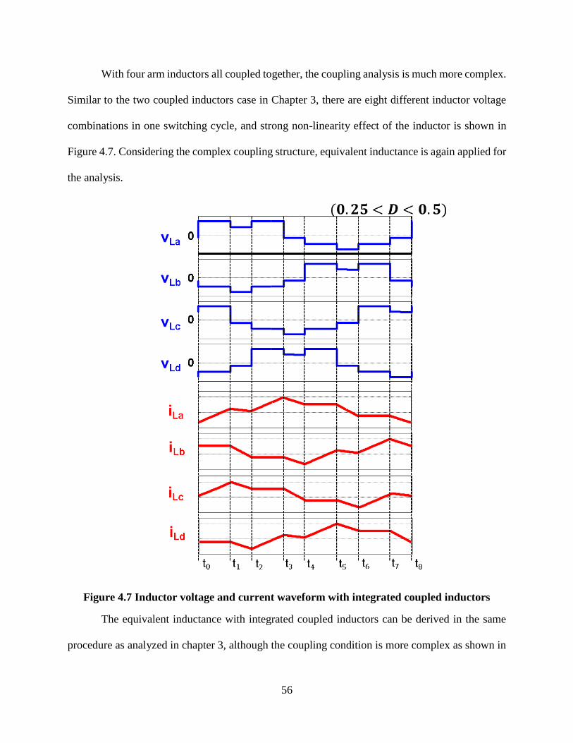
56
With four arm inductors all coupled together, the coupling analysis is much more complex.
Similar to the two coupled inductors case in Chapter 3, there are eight different inductor voltage
combinations in one switching cycle, and strong non-linearity effect of the inductor is shown in
Figure 4.7. Considering the complex coupling structure, equivalent inductance is again applied for
the analysis.
Figure 4.7 Inductor voltage and current waveform with integrated coupled inductors
The equivalent inductance with integrated coupled inductors can be derived in the same
procedure as analyzed in chapter 3, although the coupling condition is more complex as shown in

57
(4.4). If the relationship between the four inductor voltages can be found, the four arm inductors
can be mathematically decoupled from (4.4). It should be noted that analysis is still based on the
N-type interleaving condition.
To find the inductor voltage relationship, the equivalent circuit of the converter is drawn
first in Figure 4.8.
Figure 4.8 Equivalent circuit of the converter with integrated coupled inductors
(4.4) can be reorganized to (4.5) without assumptions that,
(4.5)
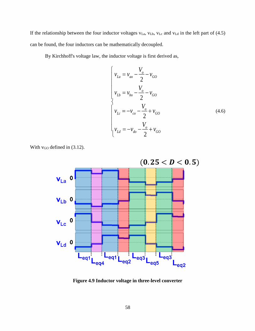
58
If the relationship between the four inductor voltages vLa, vLb, vLc and vLd in the left part of (4.5)
can be found, the four inductors can be mathematically decoupled.
By Kirchhoff's voltage law, the inductor voltage is first derived as,
2
2
2
2
oLa ao GO
oLb bo GO
oLc co GO
oLd do GO
Vv v v
Vv v v
Vv v v
Vv v v
(4.6)
With vGO defined in (3.12).
Figure 4.9 Inductor voltage in three-level converter

59
Figure 4.9 gives the inductor voltage within one switching cycle when duty ratio
0.25<D<0.5 with N-type interleaving. Based on these inductor voltage waveforms, equivalent
inductance can be derived. For other duty cycle conditions, there are also eight different time
intervals, and the analysis method is similar.
The first time interval in Figure 4.9 is used as an example to demonstrate the process of
deriving equivalent inductance. From both circuit and waveform, one can easily find that,
2
2
2
2
04
in inLa
inLb
in inLc
inLd
ao bo co doGO
V DVv
DVv
V DVv
DVv
v v v vv
(4.7)
By take (4.7) into (4.5), one can decouple the matrix of inductor equation (4.5), and the
relationship for inductor voltage and current of each arm can be directly connected. (4.5) becomes,
(4.8)
And

60
(1 )( )( 2 )
(1 )
x x y LaLa
x y
D L M L M M div
L D M D M dt
(4.9)
And now the equivalent inductance is defined as,
1
(1 )( )( 2 )
(1 )
x x y
eq
x y
D L M L M ML
L D M D M
(4.10)
Note the equivalent inductance is defined based on arm a. For the equivalent inductance on arm b,
c and d, the only difference would be a 90 degree phase shift due to the N-type interleaving.
Because of the positive-coupling of the integrated coupled inductors, the equivalent inductance is
quite different compared to the two separated coupled inductors case, which is analyzed in chapter
3.
By going over the eight time intervals within one switching cycle one by one, there are five
different equivalent inductances within one switching cycle, as shown in the shaded area of
different color in Figure 4.9.
1
2
3
4
5
(1 )( )( 2 )
(1 )
2
( )( 2 )
(1 )
(3 4 )( )( 2 )
(3 4 ) (4 1)
(1 4 )( )( 2 )
(1 4 ) (3 4 )
x x y
eq
x y
eq x y
x x y
eq
x y
x x y
eq
x y
x x y
eq
x y
D L M L M ML
L D M D M
L L M M
D L M L M ML
LD M D M
D L M L M ML
L D M D M
D L M L M ML
L D M D M
(4.11)
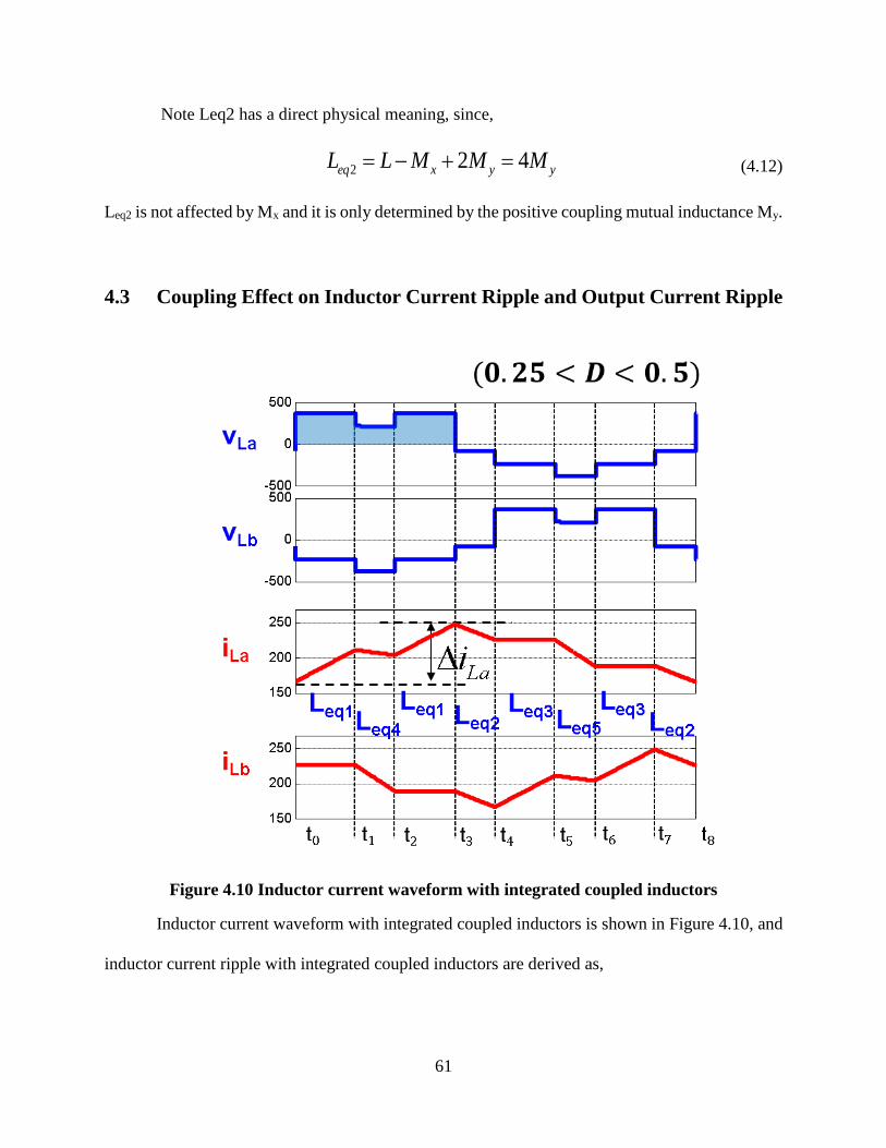
61
Note Leq2 has a direct physical meaning, since,
2 2 4eq x y yL L M M M (4.12)
Leq2 is not affected by Mx and it is only determined by the positive coupling mutual inductance My.
4.3 Coupling Effect on Inductor Current Ripple and Output Current Ripple
Figure 4.10 Inductor current waveform with integrated coupled inductors
Inductor current waveform with integrated coupled inductors is shown in Figure 4.10, and
inductor current ripple with integrated coupled inductors are derived as,

62
31 2
1 4 1
LaLa La TT TLa
eq eq eq
vv vi
L L L
(4.13)
Similar to the two coupled inductors case in chapter 3, inductor current ripple with
integrated coupled inductors is also determined by the first three time intervals. To have a fair
comparison with the two coupled inductors case, the steady-state equivalent inductance
determining the inductor current ripple is defined,
1 2 3 1 2 3
31 2
1 4 1
La La La La La LaT T T T T Tss
LaLa LaLa TT T
eq eq eq
v v v v v vL
vv vi
L L L
(4.14)
With simple mathematical derivation, (4.14) becomes,
2
2 2
( 8 10 1)( )( 2 )
( 8 10 1) (8 2 1) 8
x x y
ss
x y
D D L M L M ML
D D L D D M DM
(4.15)
For the output current ripple, the relationship with equivalent inductance can be observed
from the current waveform directly in Figure 4.11. In the time interval t3-t4, both inductor current
ripples iLa and iLb are determined by Leq2, and the overall output current ripple is also solely
determined by Leq2, or 4My. The same conclusion can be drawn for other duty cycle ranges.
4 4
2 2
La LbT To
eq eq
v vi
L L
(4.16)
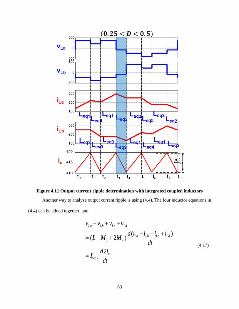
63
Figure 4.11 Output current ripple determination with integrated coupled inductors
Another way to analyze output current ripple is using (4.4). The four inductor equations in
(4.4) can be added together, and
2
( )( 2 )
2
La Lb Lc Ld
La Lb Lc Ldx y
oeq
v v v v
d i i i iL M M
dt
d iL
dt
(4.17)
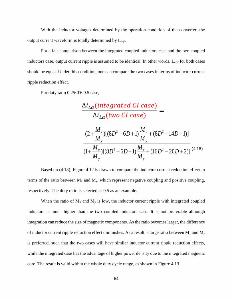
64
With the inductor voltages determined by the operation condition of the converter, the
output current waveform is totally determined by Leq2.
For a fair comparison between the integrated coupled inductors case and the two coupled
inductors case, output current ripple is assumed to be identical. In other words, Leq2 for both cases
should be equal. Under this condition, one can compare the two cases in terms of inductor current
ripple reduction effect.
For duty ratio 0.25<D<0.5 case,
2 2
2 2
(2 )[(8 6 1) (8 14 1)]
(1 )[(8 6 1) (16 20 2)]
x x
y y
x x
y y
M MD D D D
M M
M MD D D D
M M
(4.18)
Based on (4.18), Figure 4.12 is drawn to compare the inductor current reduction effect in
terms of the ratio between Mx and My, which represent negative coupling and positive coupling,
respectively. The duty ratio is selected as 0.5 as an example.
When the ratio of Mx and My is low, the inductor current ripple with integrated coupled
inductors is much higher than the two coupled inductors case. It is not preferable although
integration can reduce the size of magnetic components. As the ratio becomes larger, the difference
of inductor current ripple reduction effect diminishes. As a result, a large ratio between Mx and My
is preferred, such that the two cases will have similar inductor current ripple reduction effects,
while the integrated case has the advantage of higher power density due to the integrated magnetic
core. The result is valid within the whole duty cycle range, as shown in Figure 4.13.

65
Figure 4.12 Inductor current ripple comparison
Figure 4.13 Inductor current ripple comparison within whole duty cycle range

66
4.4 Coupling Design based on Current Ripple Requirement
As discussed in section 4.1, two types of coupling effects exist in integrated coupled
inductors and should be properly designed. Mutual inductance Mx represents the negative coupling
effect to suppress the circulating current, and mutual inductance My represents the positive
coupling effect to reduce the output current ripple. And the self-inductance L=Mx+2My.
The coupling of integrated coupled inductors should be designed based on the performance
requirement of the converter. Through the equivalent inductance analysis, the inductor current
ripple and output current ripple equation is,
2
2
2
2
(1 4 )0.25
4
(4 1)(1 2 ) 0.25 0.5
8
(3 4 )(2 1) 0.5 0.75
8
(4 3)(1 ) 0.75 1
4
dc
dc
eq
e
o
d
q
eq
eq
c
dc
V DDT D
V DD T D
iV D
D T D
V DD
L
L
T D
L
L
(4.19)
(1 4 )0.25
32 4(2 2 )
(4 1)(1 2 ) 0.25 0.5
64 4(2 2 )
(3 4 ) (1 )(2 1) 0.5 0.75
64 4(2 2 )
(4 3) (1 )(1 ) 0.75
32 4(2 2 )
dc dc
dc dc
La
dc dc
dc d
y x y
y x y
y
x
c
y x
y y
V D V DDT T D
V D V DD T T D
iV D V D
D T T D
V D V
M
DD T T
M M
M M M
M M M
M M MD
(4.20)
The design process includes two steps. Since the Leq2 determines the output current ripple
and equals to 4My, the mutual inductance My can be designed directly with the output current

67
ripple requirement. With My determined, mutual inductance Mx will be designed based on the
inductor current ripple requirement. Input voltage Vdc=1200V, switching frequency fsw=1/T=20
kHz, power rating P=200kW.
In the first step, Leq2 is designed based on the output current ripple, which is the same
process as the two coupled inductors case in section 3.4. The only difference is that now Leq2=4My.
From Figure 4.14, the maximum output current ripple can be calculated by sweeping different Leq2
value, and Figure 4.15 can be drawn accordingly. If the required maximum output current ripple
is given, for example 16A, the designed Leq2 will be 60μH. In other words, the designed mutual
inductance My should be larger than 15μH to guarantee the maximum output current ripple to be
less than 16A.
Figure 4.14 Output current ripple with different Leq2

68
Figure 4.15 Design Leq2 based on output current ripple
With My value determined, mutual inductance Mx could be designed based on the inductor
current ripple requirement.
Figure 4.16 Inductor current ripple with different Mx

69
With My=15μH, the inductor current ripple can be plotted using (4.20) in Figure 4.16. By
sweeping the maximum inductor current ripple with different Mx values, Figure 4.17 is drawn. Mx
is designed at the corner of the curve for 500μH to guarantee the maximum inductor current ripple
of 13A.
Figure 4.17 Design Mx based on inductor current ripple
Followed by the two steps above, Mx=500μH, My=15μH is designed for the 16A output
current ripple and 13A inductor current ripple.
Simulation is used the check the analysis result. The integrated coupled inductors indicated
in the shaded area of Figure 4.18 is simulated using six ideal transformers. Figure 4.18 gives the
converter circuit, and the parameters are input voltage Vin=1200V, output voltage Vo=480, duty
ratio D=0.4, switching frequency fsw=20kHz, and power rating P=200kW. As shown in Figure
4.19, the different coupling effects among the four arms a, b c and d are represented by ideal
transformers, with the magnetizing inductance equal to the mutual inductance designed.

70
Figure 4.18 Three-level DC/DC Converter with integrated coupled inductors
Figure 4.19 Simulation circuit model for integrated coupled inductors
Figure 4.20 Simulation waveform of inductor current and output current

71
In the simulation result of Figure 4.20, both inductor current ripple and output current
ripple are within the design target, which is ΔiLa=13A, Δio=15A.
4.5 Magnetic Circuit Analysis
Considering the three-dimensional structure of the integrated coupled inductors, the proper
air gap should be used to guarantee the required positive coupling and negative coupling. By Figure
4.21, the air gap of the C-C core is defined as l1 and the air gap between the center block and C-C
core is defined as l2. The relative permeability of the center block is μr. In this case the cross-
section area of C-C core is A and for center block is 2A.
Figure 4.21 Geometry of integrated coupled inductors
Based on Figure 4.21, the magnetic circuit is shown as below, with
11
0
lR
A
(4.21)
22
0 0
2
2 2
b
r
llR
A A
(4.22)

72
Figure 4.22 Magnetic circuit of integrated coupled inductors
Where R1 is the reluctance of air gap l1 and R2 is the reluctance of air gap l2 together with the
center block. It should be noted that high permeability material is used for the C-C core and its
reluctance is assumed to be neglected in the analysis.
From the magnetic circuit, the negative coupled mutual inductance Mx and positive coupled
mutual inductance My can be derived,
2
2 1
2
1 2 1
(4 )
8 4x
N R RM
R R R
(4.23)
2
1 24 8y
NM
R R
(4.24)
And the ratio representing two coupling effects is,
2 1
2 1
1 1
24
4b
x r
y
ll l
M R R
M R l
(4.25)
As stated in the previous section, the high ratio of Mx and My is preferred, such that the integrated
coupled inductors case will have comparable performance with the two coupled inductors case,
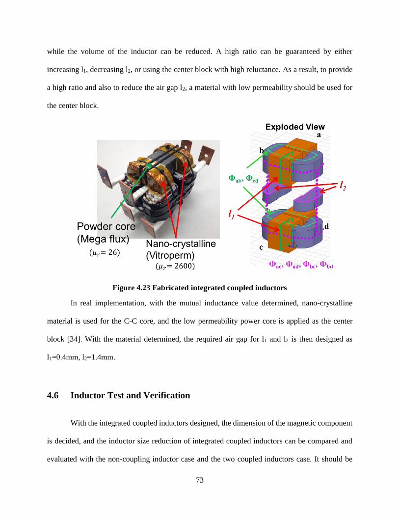
73
while the volume of the inductor can be reduced. A high ratio can be guaranteed by either
increasing l1, decreasing l2, or using the center block with high reluctance. As a result, to provide
a high ratio and also to reduce the air gap l2, a material with low permeability should be used for
the center block.
Figure 4.23 Fabricated integrated coupled inductors
In real implementation, with the mutual inductance value determined, nano-crystalline
material is used for the C-C core, and the low permeability power core is applied as the center
block [34]. With the material determined, the required air gap for l1 and l2 is then designed as
l1=0.4mm, l2=1.4mm.
4.6 Inductor Test and Verification
With the integrated coupled inductors designed, the dimension of the magnetic component
is decided, and the inductor size reduction of integrated coupled inductors can be compared and
evaluated with the non-coupling inductor case and the two coupled inductors case. It should be

74
noted that the three scenarios are compared with the same inductor current ripple and output
current ripple conditions.
The first scenario is non-interleaving three-level DC/DC converter with non-coupling
inductors, and four single inductors are required for the converter. The second scenario is N-type
interleaving with two separate coupled inductors, and the last scenario is N-type interleaving with
integrated coupled inductors. Figure 4.24 gives the converter circuit and corresponding 3-D
inductor structure. With integrated structure, the volume for magnetics is 3.95L, which is only half
of the inductor size in non-coupling inductor case [34]. Therefore, the integration of magnetics
brings benefits of increased power density and better ripple performance.
Figure 4.24 Inductor size comparison
With the fabricated integrated coupled inductors, it is crucial to have the inductor tested
and verified first to see if it can fulfill the mutual inductance requirements, as mentioned in the
previous section.

75
The verification process includes two parts: the test of negative coupling mutual inductance
Mab & Mcd, and the test of positive coupling mutual inductance Mac, Mad, Mbc & Mbd. As the
inductor is assumed to be a symmetrical structure, here Mx=Mab=Mcd and My=Mac=Mad=Mbc=Mbd
will be set as variables for the test. Also, the self-inductance can be calculated using (4.2) if needed.
Figure 4.25 gives the structure of the integrated coupled inductors with eight terminals. a1, b1, c1,
d1 represent four terminals connecting to the phase legs side, while a2, b2, c2, d2 represent four
terminals connecting to the output side.
Figure 4.25 Fabricated integrated coupled inductors for test
Figure 4.26 Test circuit for My
76
To test the mutual inductance My, the inductor is configured in the left-side circuit in Figure
4.26. Arm a and b are connected in parallel, and then connecting with arm c & d paralleled in
series. Under this condition,
La Lb Lc Ldi i i i (4.26)
La Lb Lc LdLa x y y
di di di div L M M M
dt dt dt dt (4.27)
Put (4.26) into (4.27),
( ) 4 La LaLa x y y y
di div L M M M M
dt dt (4.28)
Now integrated coupled inductors are decoupled and the same conclusion can be drawn for
the other three arms b, c & d. As a result, the right-side circuit in Figure 4.26 is derived for the
representation of decoupled inductors. For all four arms a, b, c & d, the inductance is just 4My.
And the tested inductance Ltest is,
4test yL M (4.29)
Figure 4.27 and Figure 4.28 give the tested inductance Ltest result from impedance analyzer
and single pulse test, respectively. From both test methods, the measured inductance is about 60μH,
or the mutual inductance My is 15μH, which is the design target to meet the current ripple
requirement. Also note the saturation current is over 800A.

77
Figure 4.27 Test result for My with impedance analyzer
Figure 4.28 Test result for My with single pulse test

78
As the second test step, the mutual inductance Mx needs verification, and its test circuit is
shown in the left part of Figure 4.29. Arm a and arm b are connected in series, with arm c and d
left open.
Figure 4.29 Test circuit for Mx
Under this condition,
, 0La Lb Lc Ldi i i i (4.30)
By taking (4.30) into (4.27),
( ) (2 2 ) La LaLa x x y
di div L M M M
dt dt (4.31)
The relationship of inductor voltage and current is built for arm a, and the conclusion for
arm b is exactly the same. As a result, under this circuit configuration, the tested inductance is just
two inductor series connected with the inductance value of 2Mx+2My, as shown in the right part
of Figure 4.29.
4 4test x yL M M (4.32)

79
Figure 4.30 Test result for Mx with impedance analyzer
Figure 4.31 Test result for Mx with single pulse test

80
With My known from the first step of the test, the mutual inductance Mx can be calculated,
which is around 800μH. Considering the current ripple requirement, 800μH is high enough for
inductor current ripple reduction.
With the above two steps, both mutual inductance Mx and My are verified to meet the
inductor current ripple and output current ripple reduction requirements.
4.7 Controller Design and Experiment Result of the Converter
For the three-level DC/DC converter with integrated coupled inductors, the proper
controller should be designed first based on the small-signal model before the hardware experiment.
For the paralleled phase legs, the small-signal model is derived by inserting three-terminal
switch model. As shown in Figure 4.32, there are four three-terminal switches, and each of them
can be replaced with the small-signal model for three-terminal switch in Figure 4.33. It should be
noted that two assumptions are made for modeling. 1). all the parasitic is neglected. 2). the
converter works under balanced neutral-point voltage and inductor current sharing condition,
2
dcpo on
VV V
(4.33)
2
oLa Lb Lc Ld
II I I I
(4.34)

81
Figure 4.32 Paralleled phase legs
Figure 4.33 Small-signal model for three-terminal switch
By applying KVL and KCL, the complete small-signal model of the converter can be much
simplified, as is shown in Figure 4.34. Considering that all parameters in the integrated coupled
inductors are symmetrical as shown in (4.4), the open-loop control-to-output transfer function can
be derived as,
d
O
o c z
2
2
0 0
s1
V s
s sR1
w Q
i
d
w
(4.35)

82
0
1
e OqL C
O
eq
O
CQ
LR
1z
O O
sC R
(4.36)
4 yeqL M (4.37)
Figure 4.34 Complete small-signal model of the converter
Figure 4.35 Open-loop control-to-output current transfer function
The derived small-signal model is verified in the bode plot Figure 4.35. The solid red line
represents the modeling derivation result, while the dash blue line represents the SIMPLIS
simulation result. The converter parameters are, input voltage Vin=1200V, duty ratio D=0.4,
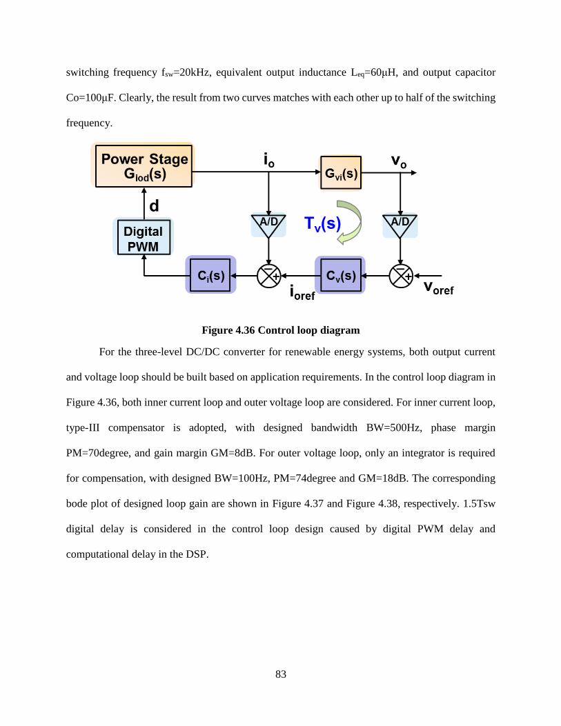
83
switching frequency fsw=20kHz, equivalent output inductance Leq=60μH, and output capacitor
Co=100μF. Clearly, the result from two curves matches with each other up to half of the switching
frequency.
Figure 4.36 Control loop diagram
For the three-level DC/DC converter for renewable energy systems, both output current
and voltage loop should be built based on application requirements. In the control loop diagram in
Figure 4.36, both inner current loop and outer voltage loop are considered. For inner current loop,
type-III compensator is adopted, with designed bandwidth BW=500Hz, phase margin
PM=70degree, and gain margin GM=8dB. For outer voltage loop, only an integrator is required
for compensation, with designed BW=100Hz, PM=74degree and GM=18dB. The corresponding
bode plot of designed loop gain are shown in Figure 4.37 and Figure 4.38, respectively. 1.5Tsw
digital delay is considered in the control loop design caused by digital PWM delay and
computational delay in the DSP.

84
Figure 4.37 Inner current loop gain bode plot
Figure 4.38 Outer voltage loop gain bode plot

85
Figure 4.39 Hardware overview for three-level DC/DC Converter
The integrated coupled inductors are tested with three-level DC/DC converter hardware,
as shown in Figure 4.39. The two phase legs constitute the two three-level buck converter, using
1200V/400A IGBT modules from Semikron. N-type interleaving is applied to reduce the output
current ripple. DC contactor and DC fuses are also applied for protection. The experimental setup
is shown in Figure 4.40.
Figure 4.40 Experimental setup
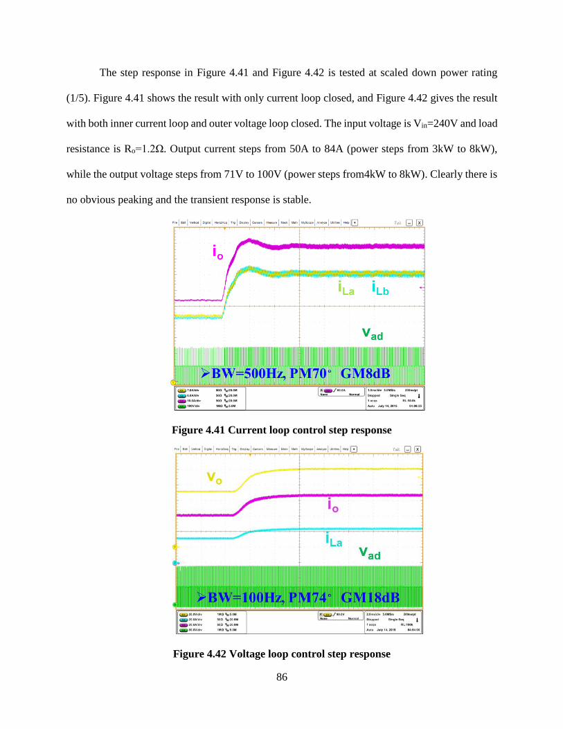
86
The step response in Figure 4.41 and Figure 4.42 is tested at scaled down power rating
(1/5). Figure 4.41 shows the result with only current loop closed, and Figure 4.42 gives the result
with both inner current loop and outer voltage loop closed. The input voltage is Vin=240V and load
resistance is Ro=1.2Ω. Output current steps from 50A to 84A (power steps from 3kW to 8kW),
while the output voltage steps from 71V to 100V (power steps from4kW to 8kW). Clearly there is
no obvious peaking and the transient response is stable.
Figure 4.41 Current loop control step response
Figure 4.42 Voltage loop control step response
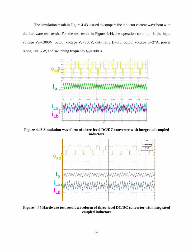
87
The simulation result in Figure 4.43 is used to compare the inductor current waveform with
the hardware test result. For the test result in Figure 4.44, the operation condition is the input
voltage Vin=1000V, output voltage Vo=600V, duty ratio D=0.6, output voltage Io=27A, power
rating P=16kW, and switching frequency fsw=20kHz.
Figure 4.43 Simulation waveform of three-level DC/DC converter with integrated coupled
inductors
Figure 4.44 Hardware test result waveform of three-level DC/DC converter with integrated
coupled inductors

88
Clearly, the test waveform matches with the simulation result. The phase leg output voltage
vad is a three-level waveform and the inductor current iLa and iLb has a zig-zag shape due to the
non-linear inductance within one switching cycle.
4.8 Summary
By using the equivalent inductance analysis method, this chapter provides a systematical
way to design the integrated coupled inductors fulfilling the current ripple requirements.
Since two coupled inductors are required for paralleled three-level DC/DC converter, a
novel integrated coupled inductors structure is adopted to reduce the size of the magnetic
components. Instead of the conventional negatively coupled inductors, now the leakage flux are
positively coupled together and there are two types of coupling effects in the integrated coupled
inductors. The negative coupling effect is aimed at reducing the circulating current between two
phase legs, while the positive coupling effect is aimed at increasing the output inductance and
reduce the output current ripple.
Similar to the conventional coupled inductors, the integrated coupled inductors case has
the characteristics of non-linear inductance within one switching cycle. Based on the equivalent
inductance analysis, the relationship between the current ripple and equivalent inductance is built,
and it provides a clear method to determine the negative and positive coupled mutual inductance
desired for inductor current ripple and output current ripple reduction targets. A prototype of
integrated coupled inductors is built with nano-crystalling C-C core and powder block core, with
air gaps finely designed to meet the inductance value requirements.
Comparing the solution with the two coupled inductors case for three-level DC/DC
converter, the integrated coupled inductors case has the benefit of greatly increased power density.

89
Under the identical current ripple performance condition, the case with integrated coupled
inductors can reduce the size of the magnetics by almost fifty percent.
A paralleled three-level DC/DC converter platform is built and the fabricated integrated
coupled inductors are tested in hardware experiment to verify its function within the converter.

90
Chapter 5 Conclusion and Future Work
5.1 Conclusion
The multi-phase three-level DC/DC converter with integrated coupled inductors is
demonstrated and analyzed in this paper to elaborate its benefit as a high-power, high-voltage
converter for renewable energy applications including the battery storage system, PV farm and
electric vehicle charge station. Together with a three-phase three-level AC/DC inverter stage, the
two-stage three-level power conversion system has the benefit of high power density, high
efficiency with modularized structure and bi-directional power flow.
In this paper, a two-phase three-level structure is adopted to fulfill the high power rating
requirement for DC/DC stage. Compared with the conventional non-interleaving case, interleaving
for the two phase legs has the ripple cancelling effect, and output current ripple of the converter
can be reduced. From the analysis in Chapter 2, N-type interleaving is more advantageous than
non-interleaving and Z-type interleaving methods in terms of current ripple and common-mode
noise. To solve the issue of huge circulating current between two phase legs caused by interleaving,
usually negative coupled inductors are applied together with the interleaving method to suppress
circulating current and maintain good ripple performance.
Due the negative coupling, the inductor becomes a non-linear one within one switching
cycle, and equivalent inductance can be defined with different inductor voltage combinations.
Through the inductor current and output waveform analysis, the relationship between the
equivalent inductance and current ripple can be built, and coupling can be designed based on the
inductor current ripple and output current ripple targets. With the same output current ripple, the
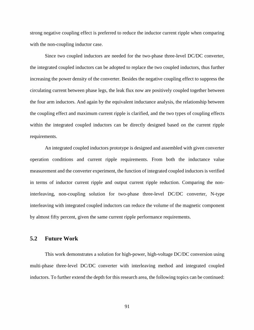
91
strong negative coupling effect is preferred to reduce the inductor current ripple when comparing
with the non-coupling inductor case.
Since two coupled inductors are needed for the two-phase three-level DC/DC converter,
the integrated coupled inductors can be adopted to replace the two coupled inductors, thus further
increasing the power density of the converter. Besides the negative coupling effect to suppress the
circulating current between phase legs, the leak flux now are positively coupled together between
the four arm inductors. And again by the equivalent inductance analysis, the relationship between
the coupling effect and maximum current ripple is clarified, and the two types of coupling effects
within the integrated coupled inductors can be directly designed based on the current ripple
requirements.
An integrated coupled inductors prototype is designed and assembled with given converter
operation conditions and current ripple requirements. From both the inductance value
measurement and the converter experiment, the function of integrated coupled inductors is verified
in terms of inductor current ripple and output current ripple reduction. Comparing the non-
interleaving, non-coupling solution for two-phase three-level DC/DC converter, N-type
interleaving with integrated coupled inductors can reduce the volume of the magnetic component
by almost fifty percent, given the same current ripple performance requirements.
5.2 Future Work
This work demonstrates a solution for high-power, high-voltage DC/DC conversion using
multi-phase three-level DC/DC converter with interleaving method and integrated coupled
inductors. To further extend the depth for this research area, the following topics can be continued:

92
1). Study the design of integrated coupled inductors with different magnetic materials to
optimize its power density, performance and efficiency.
2). Expand the concept of integrated magnetics to three-phase three-level interleaved
DC/DC converter. A systematical magnetic design method using equivalent inductance analysis
can be developed for three-phase interleaving, or even for four-phase interleaving DC/DC
conversion.
3). Study the control strategy for the three-level power conversion system, including both
the DC/AC inversion stage and the DC/DC conversion stage, and the possible issues for the
interaction of the two stages in control.

93
References
[1] Yu Du, Xiaohu Zhou, Sanzhong Bai, Srdjan Lukic and Alex Huang, “Review of non-
isolated bi-directional DC/DC converters for plug-in hybrid electric vehicle charge station
application at municipal parking decks”, Applied Power Electronics Conference and
Exposition (APEC), 2010 Twenty-Fifth Annual IEEE
[2] Kevork Haddad, “Three Level DC/DC Converters as Efficient Interface in Two Stage PV
Power Systems”, Energytech, 2012 IEEE
[3] A. Lachichi, “DC/DC Converters for High Power Application: A Survey”, Electric Power
and Energy Conversion Systems (EPECS), 2013 3rd International Conference on
[4] M. Hirakawa, Y. Watanabe, M. Nagano, K. Andoh, S. Nakatomi, S. Hashino, Honda R&D
Co., Ltd, “High Power DC/DC Converter using Extreme Close-Coupled Inductors aimed
for Eletric Vehicles”, IPEC 2010
[5] Kansuke Fuji, Peter Koellensperger, Rik W. De Doncker, “Characterization and
Comparison of High Blocking Voltage IGBTs and IEGTs under Hard- and Soft-Switching
Conditions”, Power Electronics Specialists Conference, 2006. PESC '06. 37th IEEE
[6] Akira Nabae, Isao Takahashi, Hirofumi Akagi, “A New Neutral-Point-Clamped PWM
Inverter”, IEEE Transactions on Industry Applications, 1981
[7] J. Renes Pinheiro and Ivo Barbi, “The three-level ZVS PWM converter-a new concept in
high voltage DC-to-DC conversion”, Industrial Electronics, Control, Instrumentation, and
Automation, 1992. Power Electronics and Motion Control., Proceedings of the 1992
International Conference on

94
[8] Hideyuki Okui and Hisaichi Irie, “New NPC multi-level four-quadrant DC/DC converter
controlled by the integrated-voltage-control method”, Power Conversion Conference -
Nagaoka 1997., Proceedings of the (Volume:2 )
[9] T.A. Meynard, H. Foch, “Multi-level conversion: high voltage choppers and voltage-
source inverters”, Power Electronics Specialists Conference, 1992. PESC '92 Record., 23rd
Annual IEEE
[10] Ke Jin, Mengxiong Yang and Xinbo Ruan, “Three-Level Bi-Directional Converter — A
Novel DC/DC Converter Suitable for Fuel Cell Power System”, Power Electronics
Specialists Conference, 2006. PESC '06. 37th IEEE
[11] Zhang, M.T., et al. “Single-phase three-level boost power factor correction converter”. in
Applied Power Electronics Conference and Exposition, 1995. APEC '95. Conference
Proceedings 1995., Tenth Annual. 1995. Dallas, TX.
[12] Petar J. Grbovic, et al. “A Bidirectional Three-Level DC–DC Converter for the
Ultracapacitor Applications”, Industrial Electronics, IEEE Transactions on (Volume:57 ,
Issue: 10 ), 2010
[13] Fang Zheng Peng, “A Generalized Multilevel Inverter Topology with Self Voltage
Balancing”, Industry Applications, IEEE Transactions on (Volume:37 , Issue: 2 )
[14] Xinbo Ruan, Bin Li, and Qianhong Chen, “Three-level converters-a new approach for high
voltage and high power DC-to-DC conversion”, Power Electronics Specialists Conference,
2002. pesc 02. 2002 IEEE 33rd Annual (Volume:2 )
[15] Xinbo Ruan, Bin Li, Qianhong Chen, Siew-Chong Tan, Chi K. Tse, “Fundamental
Considerations of Three-Level DC/DC Converters: Topologies, Analyses, and Control”,
Circuits and Systems I: Regular Papers, IEEE Transactions on (Volume:55 , Issue: 11 )
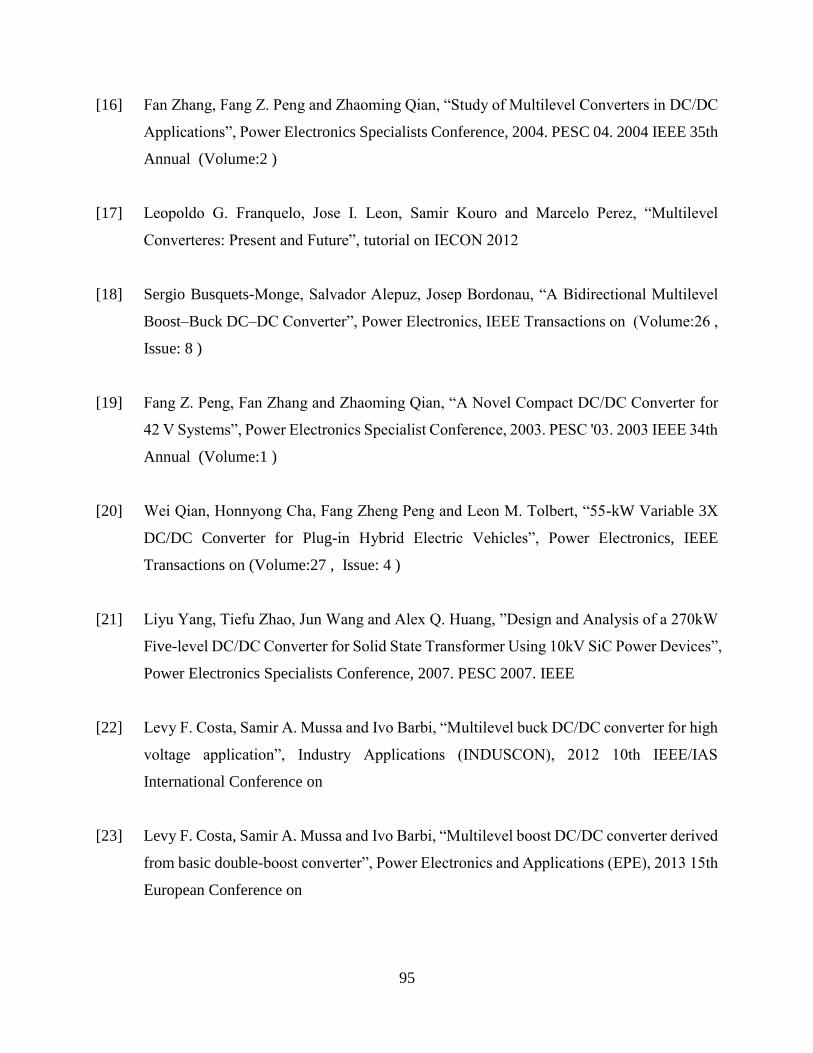
95
[16] Fan Zhang, Fang Z. Peng and Zhaoming Qian, “Study of Multilevel Converters in DC/DC
Applications”, Power Electronics Specialists Conference, 2004. PESC 04. 2004 IEEE 35th
Annual (Volume:2 )
[17] Leopoldo G. Franquelo, Jose I. Leon, Samir Kouro and Marcelo Perez, “Multilevel
Converteres: Present and Future”, tutorial on IECON 2012
[18] Sergio Busquets-Monge, Salvador Alepuz, Josep Bordonau, “A Bidirectional Multilevel
Boost–Buck DC–DC Converter”, Power Electronics, IEEE Transactions on (Volume:26 ,
Issue: 8 )
[19] Fang Z. Peng, Fan Zhang and Zhaoming Qian, “A Novel Compact DC/DC Converter for
42 V Systems”, Power Electronics Specialist Conference, 2003. PESC '03. 2003 IEEE 34th
Annual (Volume:1 )
[20] Wei Qian, Honnyong Cha, Fang Zheng Peng and Leon M. Tolbert, “55-kW Variable 3X
DC/DC Converter for Plug-in Hybrid Electric Vehicles”, Power Electronics, IEEE
Transactions on (Volume:27 , Issue: 4 )
[21] Liyu Yang, Tiefu Zhao, Jun Wang and Alex Q. Huang, ”Design and Analysis of a 270kW
Five-level DC/DC Converter for Solid State Transformer Using 10kV SiC Power Devices”,
Power Electronics Specialists Conference, 2007. PESC 2007. IEEE
[22] Levy F. Costa, Samir A. Mussa and Ivo Barbi, “Multilevel buck DC/DC converter for high
voltage application”, Industry Applications (INDUSCON), 2012 10th IEEE/IAS
International Conference on
[23] Levy F. Costa, Samir A. Mussa and Ivo Barbi, “Multilevel boost DC/DC converter derived
from basic double-boost converter”, Power Electronics and Applications (EPE), 2013 15th
European Conference on

96
[24] Levy F. Costa, Samir A. Mussa and Ivo Barbi, “Steady-state analysis of a 5-level
bidirectional buck+boost DC/DC converter”, Industrial Electronics Society, IECON 2013
- 39th Annual Conference of the IEEE
[25] Levy F. Costa, Samir A. Mussa and Ivo Barbi, “Multilevel Buck/Boost-type DC/DC
Converter for High Power and High Voltage Application”, Industry Applications, IEEE
Transactions on (Volume:PP , Issue: 99 )
[26] David Reusch, Fred C. Lee, Ming Xu, “Three Level Buck Converter with Control and Soft
Startup”, Energy Conversion Congress and Exposition, 2009. ECCE 2009. IEEE
[27] Yang Jiao, Sizhao Lu, Fred C. Lee, “Switching Performance Optimization of a High Power
High Frequency Three-Level Active Neutral Point Clamped Phase Leg”, Power
Electronics, IEEE Transactions on (Volume:29 , Issue: 7 ), 2014
[28] Robert M. Cuzner, Ashish R. Bendre, Peter J. Faill, Boris Semenov, “Implementation of a
Non-isolated Three Level DC/DC Converter Suitable for High Power Systems”, Industry
Applications Conference, 2007. 42nd IAS Annual Meeting. Conference Record of the 2007
IEEE
[29] Antonio Coccia, Franscisco Canales, “3-level interleaved boost converter assembly”,
European patent, EP 2244367 A1, 2010
[30] Sizhao Lu, Mingkai Mu, Yang Jiao and Fred C. Lee, Zhengming Zhao, “Coupled Inductors
in Interleaved Multiphase Three-Level DC–DC Converter for High-Power Applications”,
IEEE Transactions on Power Electronics ( Volume: 31, Issue: 1, Jan. 2016 )
[31] Pit-leong Wong, Peng Xu, P. Yang, Fred C. Lee, “Performance improvements of
interleaving VRMs with coupling inductors”, IEEE Transactions on Power Electronics
( Volume: 16, Issue: 4, Jul 2001 )

97
[32] Jinghai Zhou, “High Frequency, High Current Density Voltage Regulators”, dissertation,
CPES, Virginia Tech, 2005
[33] Mingkai Mu, Fred C. Lee, Yang Jiao, Sizhao Lu, “Analysis and design of coupled inductor
for interleaved multiphase three-level DC-DC converters”, Applied Power Electronics
Conference and Exposition (APEC), 2015 IEEE
[34] Mingkai Mu, Fred C. Lee, “Comparison and selection of magnetic materials for coupled
inductor used in interleaved three-level multi-phase DC-DC converters”, Energy
Conversion Congress and Exposition (ECCE), 2015 IEEE

98
Appendix A
Appendix A gives the equivalent inductance derivation result within the whole duty ratio
range for two-phase interleaved three-level DC/DC converter with coupled inductors in Chapter 3.
For 0<D<0.25, three different equivalent inductances Leq2, Leq4, Leq5 appear.
Figure A.1 Inductor current waveform with coupled inductors, 0<D<0.25
2 eq abL L M
2 2
4
( )
(1 4 )
(3 4 )
abeq
ab
L ML
DL M
D
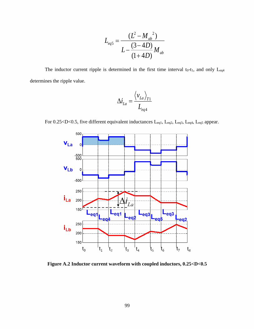
99
2 2
5
( )
(3 4 )
(1 4 )
abeq
ab
L ML
DL M
D
The inductor current ripple is determined in the first time interval t0-t1, and only Leq4
determines the ripple value.
1
4
La T
La
eq
vi
L
For 0.25<D<0.5, five different equivalent inductances Leq1, Leq2, Leq3, Leq4, Leq5 appear.
Figure A.2 Inductor current waveform with coupled inductors, 0.25<D<0.5

100
2 2
1
( )
1
abeq
ab
L ML
DL M
D
2 2
3
( )
1
abeq
ab
L ML
DL M
D
The inductor current ripple is determined in the first three time intervals t0-t3 together, and
Leq1 and Leq4 determine the ripple value.
31 2
1 4 1
LaLa La TT T
La
eq eq eq
vv vi
L L L
For 0.5<D<0.75, five different equivalent inductances Leq1, Leq2, Leq3, Leq6, Leq7 appear.
Figure A.3 Inductor current waveform with coupled inductors, 0.5<D<0.75

101
2 2
6
( )
(4 1)
(5 4 )
abeq
ab
L ML
DL M
D
2 2
7
( )
(5 4 )
(4 1)
abeq
ab
L ML
DL M
D
The inductor current ripple is determined in the last three time intervals t5-t8, and Leq3 and
Leq7 determine the ripple value together.
6 7 8
3 7 3
La La LaT T T
La
eq eq eq
v v vi
L L L
For 0.75<D<0.1,
Figure A.4 Inductor current waveform with coupled inductors, 0.75<D<0.1

102
The inductor current ripple is calculated in the last time interval t7-t8, and only Leq7
determines the ripple value.
8
7
La T
La
eq
vi
L
Note that Leq6 and Leq7 are two equivalent inductances existing in D>0.5 case only, and Leq4
and Leq5 only exist in D<0.5 case only.


![DC-DC Converter with Coupled Inductor and Multiplier Cells ... · gain is also improved by using a parallel input output series boost converter [13]. This DC-DC Converter makes use](https://static.fdocuments.net/doc/165x107/5f0b56627e708231d43004bb/dc-dc-converter-with-coupled-inductor-and-multiplier-cells-gain-is-also-improved.jpg)