STUDY ON LOSS CHARACTERISTIC OF POLYMER...
23
STUDY ON LOSS CHARACTERISTIC OF POLYMER MATERIAL FOR OPTICAL WAVEGUIDE APPLICATION ANIS SHAHIDA NIZA MOKHTAR A thesis submitted in fulfilment of the requirements for the award of the Degree of Master of Engineering (Electrical-Electronic & Telecommunication) Faculty of Electrical Engineering Universiti Teknologi Malaysia NOVEMBER 2005
Transcript of STUDY ON LOSS CHARACTERISTIC OF POLYMER...

STUDY ON LOSS CHARACTERISTIC OF POLYMER MATERIAL FOR OPTICAL WAVEGUIDE APPLICATION
ANIS SHAHIDA NIZA MOKHTAR
A thesis submitted in fulfilment of the requirements for the award of the Degree of
Master of Engineering (Electrical-Electronic & Telecommunication)
Faculty of Electrical Engineering
Universiti Teknologi Malaysia
NOVEMBER 2005

v
ABSTRACT
Communication technologies today are increasingly reliant on the
manipulation of optical signals where previously electronic circuit manipulated those
signals. With photonic technology, devices are no longer limited only to the silicon
wafer because it also not requires broader functionality than can be offered on this
traditional platform. Optical waveguides using polymer materials are attractive for
telecommunication applications due to their low costs and simple processing steps
compared to silica-based materials. Many advantages in term of optical properties
have been proved by the polymer waveguides. Polymer waveguides are potentially
useful for short distance optical interconnections. The most important characteristic
of a waveguide is the attenuation or loss experienced by light wave as it travels
through the waveguide. This dissertation focused on loss measurement of BCB
polymer waveguides. Sample of waveguides with variation thickness have been
fabricated by deposition of the polymer solution onto glass substrate. The
measurement is done by using two types of wavelength that is 630nm and 1550nm.
After analyzed all the coupling method, prism coupler method is considered as one
of the best ways to couple large amount of light in planar optical waveguides.
Furthermore it can be used to determine the loss of polymer waveguide and its
characteristics. Investigation of the polymer waveguides with respect to temperature
and water also done to see its stability.

vi
ABSTRAK
Komunikasi pada hari ini semakin beralih kepada isyarat optik yang mana
sebelum ini di manipulasi oleh litar elektronik. Dengan teknologi fotonik, peralatan
tidak lagi bergantung kepada lapisan silika kerana ia memerlukan fungsi yang lebih
luas daripada yang telah diberikan oleh platform tradisional. Pemandu gelombang
optik menggunakan polimer mempunyai daya tarikan untuk aplikasi telekomunikasi
kerana kos yang rendah dan langkah pemprosesan yang ringkas berbanding dengan
bahan berasaskan silika. Banyak kelebihan di dalam terma ciri-ciri optik yang telah
dibuktikan oleh pandu gelombang polimer. Pandu gelombang polimer berpotensi
berguna untuk sambungan optik jarak dekat. Ciri-ciri yang paling penting di dalam
pandu gelombang adalah pelemahan atau kehilangan cahaya yang merentasi pandu
gelombang polimer. Sampel pandu gelombang dengan ketebalan yang berbeza telah
di fabrikasi dengan menggunakan polimer ke atas substrat kaca. Pengiraan
dilakukan dengan menggunakan dua jenis panjang gelombang iaitu 630nm dan
1550nm. Setelah menganalisis kaedah-kaedah gandingan yang ada, kaedah
pengganding prisma adalah cara terbaik untuk menggandingkan cahaya yang banyak
di dalam pemandu gelombang polimer. Tambahan pula ia boleh digunakan untuk
menentukan kehilangan pemandu gelombang dan sifat-sifatnya. Pemandu gelombang
polimer juga di kaji terhadap kesan suhu dan air untuk melihat stabilitinya.

vii
TABLE OF CONTENTS
CHAPTER TITLE PAGE
TITLE i
DECLARATION ii
DEDICATION iii
ACKNOWLEDGEMENTS iv
ABSTRACT v
ABSTRAK vi
TABLE OF CONTENTS vii
LIST OF TABLES xi
LIST OF FIGURES xii
LIST OF SYMBOLS xv
LIST OF ABBREVIATIONS xvii
CHAPTER 1 INTRODUCTION
1.1 Introduction 1
1.2 Objectives 3
1.3 Scope Of Research 3
1.4 Methodology 4
1.5 Thesis Outline 5

viii
CHAPTER 2 WAVE THEORY OF OPTICAL WAVEGUIDES
2.1 Introduction 7
2.2 Slab Waveguide structure 8
2.3 Formation of guided modes 10
2.4 Maxwell equation 14
2.5 Cut-off Condition 20
2.6 Losses In Optical Waveguide 20
2.6.1 Scattering Losses 21
2.6.1.1 Surface Scattering Losses 22
2.6.2 Absorption Losses 25
2.6.2.1 Interband Absorption 25
2.6.2.2 Free carrier Absorption 26
2.6.3 Radiation Losses 27
2.6.3.1 Radiation Loss From Planar And Straight Channel 27
Waveguide
2.6.3.2 Radiation Loss From Curved Channel Waveguides 28
2.7 Measurement Of Waveguide Losses 29
2.7.1 End-Fire Coupling To Waveguides of Different Length 29
2.7.2 Fabry-Perot Cavity Measurement Technique 31
2.7.3 Direct Cut Back Method 33
2.7.4 Prism Coupled Loss Measurements 34
2.8 Polymeric Optical Waveguides 36
2.8.1 Polymeric Waveguide Characteristic 36
2.8.2 Polymer Waveguide For Optical Interconnects And 37
Optical Telecommunication Devices.

ix
CHAPTER 3 FABRICATION OF SLAB WAVEGUIDE
3.1 Introduction 40
3.2 B-Staged Bisbenzocyclobutene (BCB) from DOW® Chemical 41
3.3 Fabrication Process 43
3.3.1 Surface Preparation 45
3.3.2 Adhesion Promoter 46
3.3.3 BCB Coating 46
3.3.4 Hot Plate Soft Bake 48
3.3.5 Exposure 50
3.3.6 Pre-Develop Bake 51
3.3.7 Puddle Develop 51
3.3.8 Post Develop Bake 51
3.3.9 Curing Process 52
3.4 End Product 52
CHAPTER 4 PRISM COUPLING
4.1 Introduction 55
4.2 Prism coupler principle 56
4.3 Prism Design 57
4.4 Optimum Coupling 59
4.5 Experimental arrangement 59
4.6 Metricon2010 prism coupler 61
4.6.1 Measurement procedure 62

x
CHAPTER 5 RESULT AND ANALYSIS
5.1 Introduction 65
5.2 Result Of Prism Coupling At Wavelength of 630nm 66
5.3 Result Of Prism Coupling At Wavelength of 1550nm 77
5.4 Polishing Waveguide 86
5.4.1 Problems Encountered in Polishing Slab Waveguide 89
5.5 Waveguide Test Towards Thermal 89
5.6 Waveguide Test Towards Water 91
CHAPTER 6 FURTHER WORKS AND CONCLUSIONS
6.1 Further Works 93
6.2 Conclusion 94
REFERENCES 96
APPENDIX 99
xi
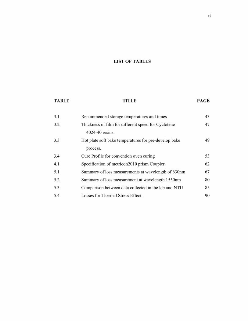
LIST OF TABLES
TABLE TITLE PAGE
3.1 Recommended storage temperatures and times 43
3.2 Thickness of film for different speed for Cyclotene 47
4024-40 resins.
3.3 Hot plate soft bake temperatures for pre-develop bake 49
process.
3.4 Cure Profile for convention oven curing 53
4.1 Specification of metricon2010 prism Coupler 62
5.1 Summary of loss measurements at wavelength of 630nm 67
5.2 Summary of loss measurement at wavelength 1550nm 80
5.3 Comparison between data collected in the lab and NTU 85
5.4 Losses for Thermal Stress Effect. 90

xii
LIST OF FIGURES
FIGURE TITLE PAGE
1.1 (a) optical-electric-optical (OEO) and (b) all optical datalink. 2
2.1 A planar slab waveguide 8
2.2 Basic structure and refractive-index profile of the optical 8
waveguide
2.3 Light ray and their phase fronts in the waveguide. 10
2.4 Total internal reflection of a plane wave at dielectric interface. 11
2.5 Formation of modes (a) fundamental modes (b) higher order modes. 13
2.6 Dispersion curves of a slab waveguide 14
2.7 Symmetric diagrams of planar dielectric waveguides. 18
2.8 diagram of ray optic approach to determination of scattering loss. 22
2.9 Diagram illustration the velocity approach to the determination 29
of radiation loss.
2.10 Schematic diagram for measurement of waveguide employing 31
end-fire coupling
2.11 Schematic view of the experiment setup for Fabry-Perot cavity 33
waveguide loss measurements. Inserts shows the detailed cavity
configuration consisting of the waveguide coupled to two
polarization maintaining fibers.
2.12 Schematic diagrams for measurement of waveguide attenuation 35
employing prism coupler
2.13 A prism is located a small distance above the guiding film. A 36
beam is incident in the prism, and under proper conditions can
couple into the waveguide.
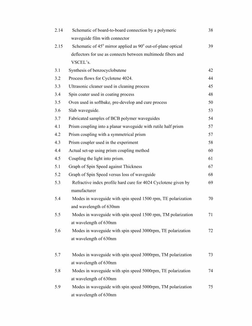
2.14 Schematic of board-to-board connection by a polymeric 38
waveguide film with connector
2.15 Schematic of 45o mirror applied as 90o out-of-plane optical 39
deflectors for use as connects between multimode fibers and
VSCEL’s.
3.1 Synthesis of benzocyclobutene 42
3.2 Process flows for Cyclotene 4024. 44
3.3 Ultrasonic cleaner used in cleaning process 45
3.4 Spin coater used in coating process 48
3.5 Oven used in softbake, pre-develop and cure process 50
3.6 Slab waveguide. 53
3.7 Fabricated samples of BCB polymer waveguides 54
4.1 Prism coupling into a planar waveguide with rutile half prism 57
4.2 Prism coupling with a symmetrical prism 57
4.3 Prism coupler used in the experiment 58
4.4 Actual set-up using prism coupling method 60
4.5 Coupling the light into prism. 61
5.1 Graph of Spin Speed against Thickness 67
5.2 Graph of Spin Speed versus loss of waveguide 68
5.3 Refractive index profile hard cure for 4024 Cyclotene given by 69
manufacturer
5.4 Modes in waveguide with spin speed 1500 rpm, TE polarization 70
and wavelength of 630nm
5.5 Modes in waveguide with spin speed 1500 rpm, TM polarization 71
at wavelength of 630nm
5.6 Modes in waveguide with spin speed 3000rpm, TE polarization 72
at wavelength of 630nm
5.7 Modes in waveguide with spin speed 3000rpm, TM polarization 73
at wavelength of 630nm
5.8 Modes in waveguide with spin speed 5000rpm, TE polarization 74
at wavelength of 630nm
5.9 Modes in waveguide with spin speed 5000rpm, TM polarization 75
at wavelength of 630nm

xiv
5.10 Result of cut-off thickness calculation for wavelength of 630nm 76
5.11 Loss for 3000rpm sample waveguide 78
5.12 Loss for 3000rpm sample waveguide 78
5.13 Loss for 5000rpm sample waveguide 79
5.14 Loss for 5000rpm sample waveguide 79
5.15 Graph of Spin Speed against Loss Waveguide. 80
5.16 Modes found in waveguide with spin speed 3000rpm, TE 81
polarization at wavelength 1550nm
5.17 Modes found in waveguide with spin speed 3000rpm, TM 82
polarization at wavelength 1550nm
5.18 Modes found in waveguide with spin speed 5000rpm, TE 83
polarization at wavelength 1550nm
5.19 Modes found in waveguide with spin speed 5000rpm, TM 84
polarization at wavelength 1550nm
5.20 Result of cut-off thickness calculation for wavelength of 1550nm 85
5.21 Waveguide before polishing process 87
5.22 Grinding machine 87
5.23 Waveguide after grinding process. 88
5.24 Waveguide after etching process. 88
5.25 Graph of Losses towards Re-Heated Waveguide. 91
5.26 Waveguide soaked in water 92
5.27 BCB coated was peeled off from substrate. 92

xv
LIST OF SYMBOLS
maxθ - Maximum Light Acceptance Angle
vρ - Current Density.
D - Electric Field Density,
φ - Propagation Angle
E - Electric Field Intensity
B - Magnetic Field Density
H - Magnetic Field Intensity
Ima x - Maximum Transmitted Intensity
Imin - Minimum Transmitted Intensity
m. - Mode Number
n1 - Refractive Index of Cladding Region
n2, nf - Refractive Index of The Thin Film
n3, ns - Refractive Index of Substrate Layer
na - Refractive Index of Air
np - Refractive Index of The Prism
r - Reflection Coefficient.
T - Transmission Reflection Coefficients
α - Attenuation Coefficient
β - Propagation Constant
ε - Permittivity of a Medium
η - Coupling Efficiency
θc - Critical Angle of Total Internal Reflection
θi - Incident Angle,
θm - Incident on The Prism Face At An Angle

xvi
κ - Coupling Coefficient.
λ - Wavelength
λc - Cutoff (free space) Wavelength
µ - Permeability of a Medium
σ2 - Variances
Ф - Phase Shift

xvii
LIST OF ABBREVIATIONS
AWG - Arrayed Waveguide Grating
AWG - Arrayed-Waveguide Grating
BCB - B-Staged Bisbenzocyclotene
NA - Numerical Aperture.
OADM - Optical Add/Drop Filter/Multiplexer
OEO - Optical-Electrical-Optical
OIC’s - Optical Integrated Circuits
PIC’s - Photonic Integrated Circuits
TDM - Time Division Multiplexing
TE - Transverse Electric
TEM - Transverse Electromagnetic Mode
TLS - Tunable Laser Source
TM - Transverse Magnetic
VCSEL’s - Vertical-Cavity Surface-Emitting-Laser
VLSI - Very Large-Scale Integrated
VOA - Variable Optical Attenuator

CHAPTER 1
INTRODUCTION
1.1 Introduction
There is a great interest in creating optical integrated circuits (OIC’s) or
photonic integrated circuits (PIC’s) that are capable of switching optical rather than
electrical signal. The fundamental difference between existing optical networks and
future all-optical networks is illustrated in Figure 1. 1. Current data networks
typically handle several signal formats by transmitting optical signals over long
distances via single-mode fibers and performing data manipulation, such as
switching and filtering, on electrical signals. Therefore, current networks require an
optical-electrical-optical (OEO) signal conversion step, one that is costly in terms of
network speed, bandwidth, power consumption, hardware complexity, and signal
integrity (noise). All-optical switching refers to the direct manipulation and routing
of optical signals without the need for an intermediate conversion to electrical signals
before switching takes place.
It is expected that future networks will avoid the OEO signal conversion step
by performing all data manipulation directly on optical signals, thereby greatly
increasing network performance. The field that will enable all-optical data

2
manipulation is referred to as integrated optics. It is envisioned that integrated optical
circuits will eventually reach a complexity similar to that of very large-scale
integrated (VLSI) electronic circuits where this electronic circuits will be replaced by
photonic circuits. With photonic technology, devices are no longer limited only to
the silicon wafer and often require broader functionality than can be offered on this
traditional platform. Recently, polymeric optical waveguide are becoming
increasingly important because of the functionality and complexity that can be
fabricated reliably at low cost with high manufacturing output.
This project discusses the fabrication and loss characterization of polymer
based optical waveguide. Slab waveguides were fabricated by deposition of polymer
onto substrate to form a film layer and spinning the substrate on the spinner to spread
the layer evenly. Different thicknesses of slab waveguide are realized by using
different spin speed. Photo BCB is used as a polymer material and the loss was
measured by using prism coupler technique. The behaviours of these polymer
waveguides are then investigated with respect to temperature and water to see its
stability. The next section in this chapter presents the objectives, scopes and research
methodology of this thesis. Description of thesis outline is presented at the end of
this section.
(a) (b)
Figure 1.1: (a) optical-electric-optical (OEO) and (b) all optical datalink.

3
1.2 Objectives
i. To fabricate polymer slab waveguide and acquire the experience on the
fabrication process
ii. To setup measurement system in order to determine the attenuation of polymer
based optical waveguide
iii. To identify possible polymer material for the purpose of developing a polymer
based optical waveguide
1.3 Scope of research
i. To understand fundamentals of related areas including optical waveguide and
optical measurement technique.
ii. To study properties of cyclotene 4024-40 photo polymer from the given
specifications.
iii. To understand and practice in house fabrication process of slab waveguide.
iv. To setup a measurement system.
v. To measure loss of the fabricated slab waveguides using setup system.
vi. To test the waveguides stability towards thermal and water
vii. To analyze measured results.

4
1.4 Methodology
Two main stages are employed in order to fulfill the objectives of this project.
The first stage is to acquire the basic knowledge about optical waveguides. Journals
and papers will be referred to enhance the understanding and to get the overview of
the projects. The second stage is to concentrate in exploring the important
characteristic in designing optical devices. In order to design an optical device, there
are many criteria that need to be considered such as the material that we want to use,
the application of the optical devices and how much cost is needed to design it. This
is followed by understanding the actual fabrication process of a polymer based
optical waveguide. There are many important properties to determine the quality of a
waveguide such as its attenuation, refractive index, birefringence, thermo optics
coefficient and thickness. This project is focused on the attenuation of polymer based
slab waveguides. Therefore simple measurement system based on the prism
coupling technique is developed. All results are collected and analyzed, and the
performances of these waveguides are then evaluated. Lastly, a report will be written
which composed of all findings, results and conclusion.

5
1.5 Thesis Outline
This thesis is organized into 6 chapters. Chapter 1 discusses the general
explanation of polymer based optical waveguide, coupling method and the
application of this polymer waveguides in the industry. The objectives that need to
Collecting Data and Analyzing
Report Writing
Setup measurement system
Validation of finding
Literature Review
Fabrication of Slab Waveguide
Meet the quality?
Yes
No

6
be achieved, the scope of research and the methodology used in this project are also
described in this chapter. In chapter 2, the theory of planar slab waveguides is
reviewed. These includes the derivation of mode in slab waveguides, the losses that
encountered in the optical waveguides and some of the measurement methods that
are used to measure loss of optical waveguides. At the end of this chapter, it will
discuss the polymeric optical waveguides, its material characteristic and the
applications. The fabrication process of slab waveguide is explained in chapter 3.
Details of every stage are clarified here. Prism coupler which is the method used in
this project is described in chapter 4. In chapter 5 the results from the measured data
are presented and analyzed. Finally the conclusions of the research will be drawn and
some suggestions for further work will be recommended in Chapter 6.

96
REFERENCES
1. Claire Piyois and Anders Hult. Absorption And Scattering In Low Loss
Polymer Optical Waveguides. J.OptSoc.Am. July 2001Vol. 18, No.7.
2. Christos Themistos, B.M Azizur Rahman,Angelos Hadjicharalambous, and
Kenneth Thomas Victor Grattan. Loss/Gain Characterization of Optical
Waveguides. IEEE J. Quantum Electron, 1995. pp.1760-1675,
3. Shee Yu Gang, Norazan Mohd. Kassim, Abu Bakar Mohammad,and Mohd
Haniff Ibrahim. Fabrication of Polymeric Optical Waveguides by B-staged
Bisbenzocyclobutene(BCB). ICSE2004. Kuala Lumpur, Malaysia, 2004
4. Shacklette, R.Blomquist,J.Deng,P.Ferm, M. Maxfield, J. Mato, P.Jiang,
K.Kilian, K.Beeson, and H.Zou. Polymer Waveguide and Device
Applications. OFC2003. Vol. 1, 2003
5. Tatsuya Yamashita, Manabu Kagami, and Hiroshilto. Waveguide shape
control and loss properties of light-induced self written (LISW) optical
waveguides, Journal of lightwave technology.2002. Vol 20
6. John. M. Senior Optical Fiber Communications, Principal And Practice.
pp.84-96, p 347-349, Prentice Hall, 1992
7. Aydin Yeniay, Renyuan Gao, Kazuka Takayama, Renfeng Gao, and Anthony
F. Garito. Ultra Low Loss Polymer Waveguides. Journal Lightwave
Technology. Vol. 22, no 1, p.154-158 ,2004
8. William H. Steier, S-S Lee, S. Gamer, A.Chen, H.Zhang, and Larry R.
Dalton. Applications Of Polymers To Integrated Optics.
9. S Monneret, P Huguet-Chantome and F Flory. M-line technique: prism
coupling measurement and discussion of accuracy for homogeneous
waveguides, j.Opt A: pure Appl. Opt 2 , p. 185-195, 2000

97
10. S. Agan F.Ay, A.Kocabas, A.Aydinli. Stress Effect In Prism Coupling
Measurement of Thin Polymer Films. Appl.Phys A.80 p 341-345, 2005.
11. Casey F. Kane and Robert R Krchnavek. Benzocyclobutene optical
waveguides IEEE Photonics Technology letters, Vol 7. 5 May 2005.
12. Polymers for encapsulation: material Processes and Reliability.
13. Aydin Yeniay, Renyuan Gao, Kazuya Takayama, Renfeng Gao and Anthony
F. Garito. ‘Ultra-Low-Loss Polymer Waveguides’, Journal of Lightwave
Technology, Vol.22, No.1, January 2004, pp.154-158.
14. Tien P.K., Ulrich R. and Martin R. J Modes of propagating Light waves in
thin deposited semiconductor films. Applied Physics Leters, 1969. 14:291-
294
15. Myung-Hyun Lee, Jung Jin Ju,Suntak, Jung Yun Do and Seong Koo Park.
Polymer-based Devices for Optical Communications ETRI Journal, Vol.
24,Number 4, pp. 259-304, August 2004
16. Dow Chemical Company. Processing Procedures for cyclotene 4000 Series
Photo BCB Resins.1999
17. Michael E. Clarke. Introducing Low-k Dielectrics into Semiconductor
Processing.2001
18. D. Navarro-Urrios et. Al .Pump-probe experiments on low loss silica
waveguides containing Si nanocrystals Mater. Res. Soc. Symp. Proc. Vol.
832. 2005
19. Edwin Y B Pun, W H Wong,.Polymeric waveguides and devices for
integrated optics applications
20. John H. Lupnski and Robert S. Moore, Silicone Gels and Coatings for
Integrated-Circuit Packaging. In polymeric material foe electronics
Packaging and Interconnection. USA:Americal Chemical Society. pp 268-
274;1989
21. M.S.Sodha and A.K.Ghatak, Inhomogeneous Optical Waveguides. New
York: Plenum Press.1977
22. Thomas Feuchter and Carsten Thirstrup. High Precision Planar Waveguide
Propagation Loss Measurement Technique Using Fabry-Perot Cavity: IEEE
Photonics Technology Letter.Vol6. Oct 1994
23. H.P. Weber, F.A. DUM and W.N. Leibolt. Appt. Optics 12 (1973) 755.
24. Y.H. Won, P.C. Janss and G.H. Chattier. Appl. Phys. Lett. 37 (1980) 269.

98
25. E.A. Aruhmyan and S.K. Galoyan, Optics Comm. 57 (1986)391.
26. Makoto Hikita, Koji Enbutsu, et.al. Polymeric Optical Waveguide Films For
Short Distance Optical Interconnects. IEEE Journal Vol. 5. No 5. Oct 1999.