STUDY OF INTERCONNECTION OF SOLAR CELLS WITHIN...
82
STUDY OF INTERCONNECTION OF SOLAR CELLS WITHIN A SOLAR PANEL TO TACKLE THE SHADING PROBLEMS TAN JIN YONG A project report submitted in partial fulfilment of the requirements for the award of Bachelor of Engineering (Hons.) Electrical and Electronic Engineering Faculty of Engineering and Science Universiti Tunku Abdul Rahman April 2016
Transcript of STUDY OF INTERCONNECTION OF SOLAR CELLS WITHIN...
STUDY OF INTERCONNECTION OF SOLAR CELLS WITHIN A SOLAR
PANEL TO TACKLE THE SHADING PROBLEMS
TAN JIN YONG
A project report submitted in partial fulfilment of the
requirements for the award of Bachelor of Engineering
(Hons.) Electrical and Electronic Engineering
Faculty of Engineering and Science
Universiti Tunku Abdul Rahman
April 2016

ii
DECLARATION
I hereby declare that this project report is based on my original work except for
citations and quotations which have been duly acknowledged. I also declare that it has
not been previously and concurrently submitted for any other degree or award at
UTAR or other institutions.
Signature :
Name :
ID No. :
Date :
iii
APPROVAL FOR SUBMISSION
I certify that this project report entitled “STUDY OF INTERCONNECTION OF
SOLAR CELLS WITHIN A SOLAR PANEL TO TACKLE THE SHADING
PROBLEMS” was prepared by TAN JIN YONG has met the required standard for
submission in partial fulfilment of the requirements for the award of Bachelor of
Engineering (Hons.) Electrical and Electronics Engineering at Universiti Tunku Abdul
Rahman.
Approved by,
Signature :
Supervisor :
Date :

iv
The copyright of this report belongs to the author under the terms of the
copyright Act 1987 as qualified by Intellectual Property Policy of Universiti Tunku
Abdul Rahman. Due acknowledgement shall always be made of the use of any material
contained in, or derived from, this report.
© 2016, Tan Jin Yong. All right reserved.

v
Specially dedicated to
my beloved mother and father,
and supervisor Dr. Lim Boon Han.

vi
STUDY OF INTERCONNECTION OF SOLAR CELLS WITHIN A SOLAR
PANEL TO TACKLE THE SHADING PROBLEMS
ABSTRACT
In recent years, the depletion of fossil fuel and the serious problem of environmental
pollution has pushed the development and uses of renewable energy. One of the most
widely use renewable energy is solar energy. Photovoltaic (PV) panel is used to
harness the solar energy and directly convert it into electricity. As solar is gaining
popularity in the recent years, many of the research had also studied to increase the
performance of PV panel. One of the biggest drawbacks for PV panel is the power
losses when subject to shading. The traditional way of solving the problem is using
bypass diodes. However, it is not efficient as the shadow can be very randomly and
unevenly. This paper aims to study various types of interconnection of solar cells in a
PV module in order to tackle the shading effect. Among all the interconnection
schemes, three interconnections are focused in this paper, which are series parallel
(SP), total cross tied (TCT) and bridge linked (BL). Additionally, this paper presents
a methodology to study the performance of different interconnection PV panels under
partial shading condition. Three PV panels were constructed and various partial
shading patterns were modelled on it, the performance is then analysed through
current-voltage curve and power–voltage curve. At the end of the paper, the result
shows that different interconnection give different power output under different partial
shadings. It is also concluded that TCT and BL configuration give significant
improvements as compared to SP configuration on power output under partial shading
condition.

vii
TABLE OF CONTENTS
DECLARATION ii
APPROVAL FOR SUBMISSION iii
ABSTRACT vi
TABLE OF CONTENTS vii
LIST OF TABLES x
LIST OF FIGURES xi
LIST OF SYMBOLS / ABBREVIATIONS xiv
LIST OF APPENDICES xv
CHAPTER
1 INTRODUCTION 1
1.1 Background and Problem Statement 1
1.2 Aims and Objectives 3
1.3 Scope 4
2 LITERATURE REVIEW 5
2.1 Solar Cell 5
2.1.1 Electrical Characteristic 5
2.1.2 Factors Affecting Solar Cell Performance 9
2.2 Solar Module 11
2.2.1 Series Connection 11
2.2.2 Parallel Connection 12
2.3 Shading 12
2.3.1 Shading Category 12
2.3.2 Shading Effect on PV Module 13
viii
2.4 Bypass Diode 15
2.5 Various Interconnection of PV Cell and PV Module 17
3 METHODOLOGY 19
3.1 Overview 19
3.2 Data Logger 21
3.2.1 Arduino Mega 2560 21
3.2.2 Adafruit Data Logging Shield 23
3.2.3 ACS712 Hall Effect Current Sensor 23
3.3 Soldering Solar Panel 24
3.3.1 Interconnection Scheme 25
3.3.2 Solar Module 26
3.4 Data Collection 26
3.4.1 Shading Pattern 27
3.4.2 PVPM1000CX I-V-Curve Tracer 31
3.5 Data Analysis 33
4 IMPLEMENTATION 34
4.1 Solar Panel 34
4.2 Data Logger and IV Curve Tracer 36
4.2.1 Voltage, Current and Power Measurement 36
4.2.2 Additional Features 40
4.2.3 Problems Encounter and Solution 41
5 Results and Discussions 45
6 CONCLUSION 57
6.1 Conclusion 57
6.2 Future Implementation 58
6.2.1 Shading Patterns and Data Collection 58
6.2.2 IV Tracer 58
REFERENCES 60

ix
APPENDICES 62

x
LIST OF TABLES
TABLE TITLE PAGE
2.1 Maximum Power and Fill Factor For 9 4 Arrays 17
2.2 Maximum Power and Fill Factor For 6 6 Arrays 18
2.3 Comparison of Peak Power and Fill Factor. 18
3.1 Specification of Arduino Mega 2560 22
3.2 Part of Specification of ACS712 24
3.3 Specification of the Solar Module 26
5.1 Power Output for Column Shading 49

xi
LIST OF FIGURES
FIGURE TITLE PAGE
2.1 Solar Cell Circuit Model 6
2.2 Power Curve of Solar Cell 8
2.3 I-V Curve with Temperature Effect 9
2.4 I-V Curve with Irradiance Effect 10
2.5 PV Curve Showing Multiple Peak 14
2.6 IV Curve with Different Number of Bypass Diodes 16
2.7 PV Module with 60 Solar Cells and 3 Bypass
Diodes 16
3.1 Flowchart of the Project 19
3.2 Arduino Mega 2560 22
3.3 Adafruit Data Logging Shield 23
3.4 ACS 712 Hall Effect Current Sensor 24
3.5 Diagram of SP, TCT and BL Interconnection
Schemes 25
3.6 Solar Module 26
3.7 2 Columns Shade 28
3.8 4 Solar Cells in a Column Shade 29
3.9 2 Solar Cells in a Row Shade 29
3.10 2 Solar Cells in Centre Shade 30
3.11 8 Solar Cells in Centre Shade 30

xii
3.12 PVPM1000CX 31
3.13 Part of Specification of PVPM1000CX 32
4.1 Front View of the Solar Panel 34
4.2 Series Parallel, Total-Cross-Tied, Bridge-Link 35
4.3 Tabbing Wire 35
4.4 Voltage Divider 37
4.5 Current Sensing Circuit 38
4.6 Complete Sensing Circuit 39
4.7 Complete Circuit of Data Logger 39
4.8 LCD Display 41
4.9 Logged Data by Arduino Data Logger 42
4.10 IV Curve by Arduino Data Logger 43
5.1 IV Curve for No Shading 45
5.2 PV Curve for No Shading 46
5.3 IV Curve for 1 Columns Shading 46
5.4 PV Curve for 1 Columns Shading 47
5.5 IV Curve for 2 Columns Shading 47
5.6 PV Curve for 2 Columns Shading 48
5.7 IV Curve for 3 Columns Shading 48
5.8 PV Curve for 3 Columns Shading 49
5.9 IV Curve for TCT Columns Shading 50
5.10 PV Curve for TCT Columns Shading 50
5.11 IV Curve for 1 Row Shading 51
5.12 PV Curve for 1 Row Shading 51
5.13 IV Curve for 4 Cells in a Column Shading 52

xiii
5.14 PV Curve for 4 Cells in a Column Shading 52
5.15 IV Curve for 2 Cells in a Row Shading 53
5.16 PV Curve for 2 Cells in a Row Shading 54
5.17 IV Curve for 2 Cells in Centre Shading 54
5.18 PV Curve for 2 Cells in Centre Shading 55
5.19 IV Curve for 8 Cells in Centre Shading 56
5.20 PV Curve for 8 Cells in Centre Shading 56
xiv
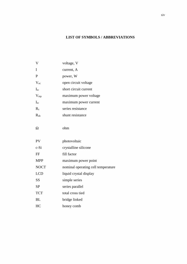
LIST OF SYMBOLS / ABBREVIATIONS
V voltage, V
I current, A
P power, W
Voc open circuit voltage
Isc short circuit current
Vmp maximum power voltage
Isc maximum power current
Rs series resistance
Rsh shunt resistance
Ω ohm
PV photovoltaic
c-Si crystalline silicone
FF fill factor
MPP maximum power point
NOCT nominal operating cell temperature
LCD liquid crystal display
SS simple series
SP series parallel
TCT total cross tied
BL bridge linked
HC honey comb
xv
LIST OF APPENDICES
APPENDIX TITLE PAGE
A Coding 62
CHAPTER 1
1 INTRODUCTION
1.1 Background and Problem Statement
In the past few years, the world used to rely heavily on fossil fuel to generate electricity
to meet the fast growing demand. Fossil fuels are non-renewable energy and this non-
renewable energy will eventually dwindle and becoming too expensive to be harnessed.
Moreover, fossil fuels is also one of the main causes of air pollution such as greenhouse
effect, acid rain, global warming and more, bringing tons of bad drawbacks to the
environment. In recent years, the rapid depletion of fossil fuel at an alarming rate as
well as the growing concern of the environmental issue has driven the world towards
employing renewable energy. Renewable energy defined as the energy that comes
from natural resources which naturally replenish such as solar, wind, water,
geothermal heat and etc. Out of all this renewable energies, most of them are comes
from the Sun energy either directly or indirectly.
The sunlight, also known as solar energy is nearly the source of all the energies
on earth. For example, the wind energy is harnessed from the air currents that flows
between two regions with a different temperature that caused by solar heat. Biomass,
an organic matter that stored energy through photosynthesis which its energy can then
be used for heating or other purposes. Even hydro energy is derived from the Sun as
we know from the hydrologic cycle. The solar energy is categorized into active solar
or passive solar by depending on the way how the solar energy is captured (Conserve
Energy Future, 2009). Active solar used special equipment to convert solar energy into
heat and electric power including photovoltaic (PV) technologies, concentrated solar
2
power and also solar water heating. On the other hand, passive solar takes the
advantage of the existing heat from Sun. Some solar passive techniques include
orientation of a building with respect to the Sun, selecting materials with favourable
thermal mass or light dispersing properties (Elza and János, 2008).
In recent year, solar energy is getting more attention from the scientist,
researchers and also social community to overcome the environmental issues as well
as the fast-growing energy demand. This is because solar energy is an abundant source
at cost free and it is environmentally friendly. A solar cell or photovoltaic (PV) cell is
used to harness the solar energy. It is an electronic device that is able to directly convert
solar irradiance into electricity. It has becoming one of the promising solutions as there
is improvisation in semiconductor technology and the advancement in power
conversion technology over the years (Mutoh, Ohno and Inoue, 2008). Due to the same
reasons, the price of PV cell had been greatly reduced and becoming more commercial.
A single PV cell is not enough to generate sufficient voltage and current for
daily commercial use. Thus, many PV cells are interconnected and encapsulated to
make a PV module. These PV cells are connected together to form an array of both
series and parallel to generate the desired output voltage and current. If the solar cells
in the module receive different levels of solar irradiance, mismatch of those cells will
happen (Wang and Hsu, 2011). A PV module power output is nonlinear and will
reduce notably if solar cell mismatch happen since solar cell has nonlinear
characteristic. One of the major factors that cause the mismatch is the shading of one
part of the PV module, also known as partial shading. The shaded solar cell will absorb
the power generated from the unshaded cell and cause localize heat that will eventually
breakdown the PV module (Petrone and Ramos-Paja, 2011).
In order to solve this problem, conventional PV modules will have bypass
diodes connected in the array of solar cells. In a conventional solar module, solar cells
are connected as a string in series to meet the desired output voltage, and then these
strings are connected in parallel to meet the current output. It will have three bypass
diodes connected in between of two strings so that if any of the strings is shaded, the
current can be bypass and minimize the power losses. However, bypass diode may also

3
cause the PV module to drop more power output even only a few cells are shaded since
the shading is random and uncertain (Bulanyi and Zhang, 2014).
Thus, this project aims to study other possible interconnection of solar cells
within the solar module so that it can tackle partial shading more effectively and thus
generating more power under various kind of shading condition. It is well aware that
various interconnection schemes had been studied by other researchers or engineers.
However, most of their research are focus on an upper level, which is the
interconnection between solar modules for PV array in a solar power plant. Different
from their project, this project will be done at a lower level at the solar cell within the
solar module which is still rarely done by other engineers. Imagine, if the maximum
power output of a single PV module can be increased by several percentage, now to
what extend the power can be yield from a PV power plant in a year.
1.2 Aims and Objectives
The main aim of the project is to study various possible interconnections of solar cells
in the solar module. A different types of interconnection of solar cells can effectively
tackle the shading loss or power mismatch loss of the PV module under different
environment condition. This project includes hardware simulation and experiment to
obtain an accurate and precise result.
As such, the objectives of this project are:
To study various possible interconnection of solar cells for a solar panel.
To construct a prototype of solar panels with different interconnection schemes.
To study the characteristic and performance of different interconnection solar
panel under partial shading conditions.

4
1.3 Scope
There are a lot of different PV cell available on the market, however, the scope of this
project will only focus on the crystalline silicon (c-Si) type of solar cell. The scope of
this project involves the research of various existing interconnection of solar cells and
understand how shading problem can affect the maximum power output of the PV
module. The project scope focuses mainly on three interconnections which are series
parallel, total cross tied and bridge link. In addition, this project will not focus on the
effect caused by bypass diode, the number of bypass diode involves in this project will
be three per modules. In chapter two, the literature review will study the different type
of possible shading and how it is going to affect the power output of each PV module
with different interconnection. The solar cell characteristic and operation, as well as
the module configurations, also presented in the literature review. In addition, this
project also includes a self-developed and designed IV tracer and data logger. The
prototype of PV modules will also be constructed to study the power output variations
under different circumstances of environment. At the end of the project, the results
obtained from the experiment is compared and analysed to determine and investigate
the interconnection configuration with highest performance under partial shading.

CHAPTER 2
2 LITERATURE REVIEW
2.1 Solar Cell
A solar cell is an electronic device that made from semiconductor materials which
having a p-n junction and is able to convert solar irradiance into electricity. The process
of converting the solar irradiance into electricity is known as photovoltaic effect. When
a sunlight is striking on the cell, the electrons gain more energy and thus jump to higher
energy level. The electrons are now free to move, leaving the holes in the materials
free to move too. When an external load is connected, the electron will flow out of the
semiconductor through the top contact. On the other hand, the holes flow through the
bottom of the cell, expecting the arrival of electrons from the top to complete the circuit.
The flow of electrons is the flow of current, and the voltage is from the internal electric
field at the p-n junction. Thus, power is generated from the solar cell when exposed to
light.
2.1.1 Electrical Characteristic
2.1.1.1 Equivalent Circuit Model
Figure 2.1 shows the equivalent solar cell circuit model. Noted that the circuit consists
of a series resistance, Rs and a shunt resistance, Rsh. Rs represents the resistances at the
metal-semiconductor interface as well as the ohmic losses in the front contacts of the

6
solar cell. While, Rsh represents the leak current of solar cell and it can cause significant
power losses. The reason of this is that Rsh will provide an alternate path for the light-
generated current to flow through which in turn result in low voltage develop in solar
cell and finally reducing the power. The voltage-current characteristic of the solar cell
can be expressed as:
𝐼 = 𝐼𝑝ℎ − 𝐼𝑜1 [𝑒𝑥𝑝 ((𝑞𝑉 + 𝐼𝑅𝑠)
𝐴𝐾𝑏𝑇𝑘) − 1] −
(𝑉 + 𝐼𝑅𝑠)
𝑅𝑠ℎ
where
𝐼 = output current
𝐼𝑜 = diode current
𝐼𝑝ℎ = 𝐼𝑠𝑐 = photon current
𝑇𝑘 = operating temperature
A = diode ideality factor
q = electron charge constant (1.602 10-19 C)
𝐾𝑏 = Boltzmann constant
Figure 2.1: Solar Cell Circuit Model
7
2.1.1.2 Open Circuit Voltage and Short Circuit Current
When the resistance is infinite, the voltage across the cell will be at its maximum,
known as the open circuit voltage, Voc. The current in the cell at this time will be zero.
Next, the short circuit current, Isc is the current that flow through the solar cell when
the resistance is zero, the cell is in short-circuited (Shukla, 2010). There will be zero
voltage across solar cell at this time and the current will reach its maximum. For an
ideal case, the short-circuit current is equal to the maximum current that can be drawn
from a solar cell. There are several factors that can affect the value of short-circuit
current. These include the area of the solar cell, the spectrum of incident light, the light
intensity, optical properties and also the collection probability of the solar cell. For
most of the case, the spectrum of light is standardise to AM1.5 and the solar cell area
is also fixed in a solar module. The intensity of the light is similar to the number of
photons available in the light or in this case, the level of solar irradiance. The
relationship between Isc and solar irradiance is directly proportional.
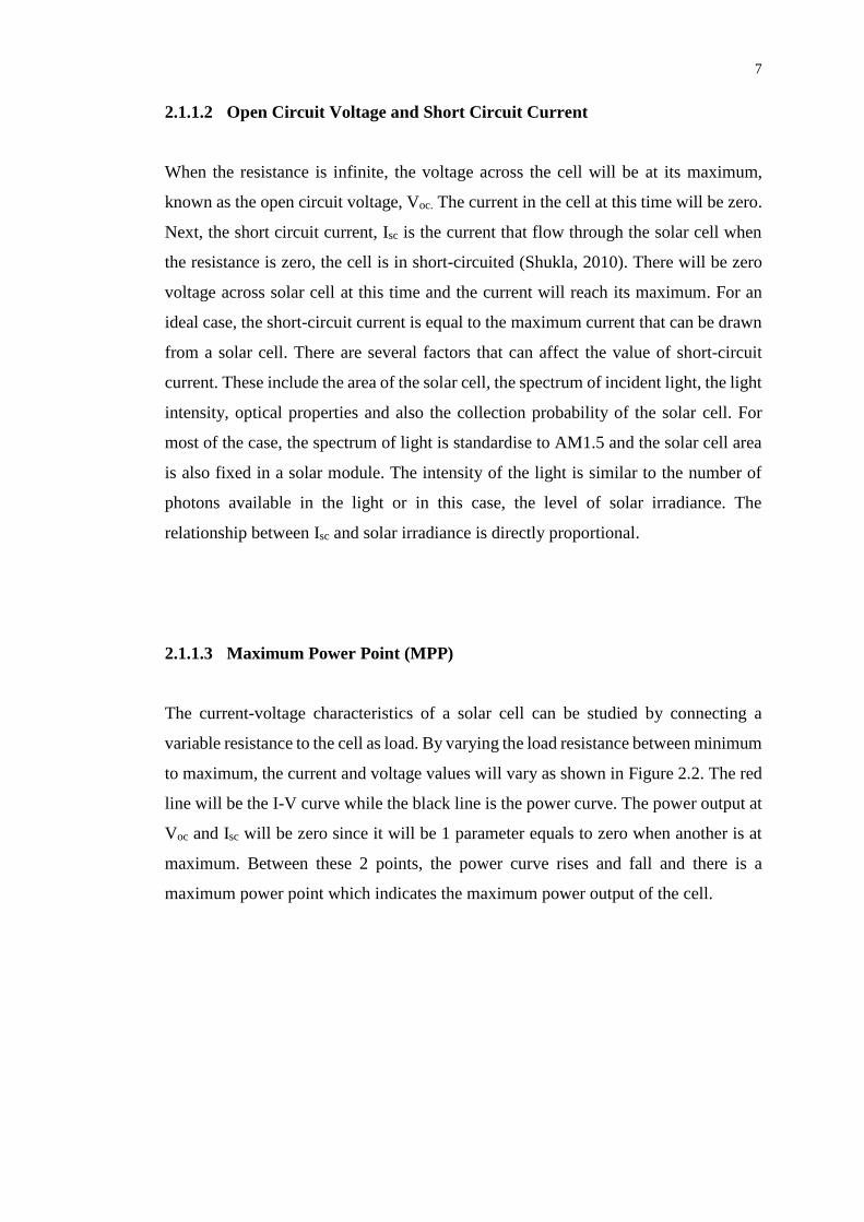
2.1.1.3 Maximum Power Point (MPP)
The current-voltage characteristics of a solar cell can be studied by connecting a
variable resistance to the cell as load. By varying the load resistance between minimum
to maximum, the current and voltage values will vary as shown in Figure 2.2. The red
line will be the I-V curve while the black line is the power curve. The power output at
Voc and Isc will be zero since it will be 1 parameter equals to zero when another is at
maximum. Between these 2 points, the power curve rises and fall and there is a
maximum power point which indicates the maximum power output of the cell.

8
Figure 2.2: Power Curve of Solar Cell
The generation of power in solar cell is the product of voltage and current, P =
IV.P is zero when either I or V are zero, which occurs at Voc and Isc respectively. When
V = Vmp and I = Imp, the maximum power, Pmp is produced, this point is known as
maximum power point (MPP) (Berning, 2011). It is essential to make sure a solar cell
is always operating at MPP or near to it so that maximum power is obtained.
2.1.1.4 Fill Factor (FF)
The Voc and Isc are the maximum voltage and current that possible to generate from a
solar cell. As a result, the product of Voc Isc is the desirable goal in delivering power
for solar cell. However since this is not possible, fill factor (FF) is a more commonly
use parameter to represent the maximum power from a solar cell. FF is explained as
the ratio of maximum output power to the product of Voc and Isc. FF = (Vmp Imp) / (Voc
Isc). As seen from Figure 2.2, FF measure the closeness of the solar cell I-V curve to
the rectangular shape. FF can also be considered as the measure of quality of a cell, a
typical FF values are in the range of 7.0 to 8.5.

9
2.1.2 Factors Affecting Solar Cell Performance
2.1.2.1 Temperature Effect
Solar cell is very sensitive to the temperature, like all others semiconductor do. The
increase in temperature will cause changes in most of the semiconductor parameters
as it decreases its band gap. The output voltage and efficiency of a solar cell increase
with the decrease of temperature. From the Figure 2.3, it is obvious that Voc decrease
as the solar cell temperature increases. However, Isc increase insignificantly. The
combined effect is the reduction of the maximum power output. Typically, the voltage
will have approximately 0.5% changes for every 1°C variation in temperature, so does
the power output.
Figure 2.3: I-V Curve with Temperature Effect
The solar cell is normally rated at the temperature of 25°C. However, the
temperature is normally higher than the ambient temperature and hence higher than
the standard test cell temperature of 25°C. Nominal operating cell temperature (NOCT)
gives better indication of the expected operating cell temperature. NOCT is defined as
the temperature reach when following conditions are met:

10
Irradiance = 800 W / m2
Ambient temperature = 20°C
Wind velocity = 1 m / s
The typical NOCT for c-Si is in the range of 45 – 50°C.
2.1.2.2 Irradiance Effect
Another factor that will affect the solar cell efficiency will be the level of sun irradiance.
The Isc had almost linear variation with the level or irradiance, but the Voc only change
slightly. Figure 2.4 shows the Isc increase as the irradiance increase, Voc does not
increase dramatically. The graph is also assuming the temperature is at constant and
not affected by the change of irradiance.
Figure 2.4: I-V Curve with Irradiance Effect
11
2.2 Solar Module
In order to achieve desired voltage and current output, solar cells are interconnected in
both series and parallel to form a PV panel, also known as solar module. Typically, a
solar module consists of 36 solar cells connected in both series and parallel (Guo, et
al., 2012). A PV module will consist of several bypass diodes as additional components
other than solar cells. The roles of bypass diode in the PV module will be explained in
the section below. Different types of interconnection between the solar cells will result
in different efficiency of PV module under partial shading condition.
2.2.1 Series Connection
If all the solar cells are connected in series in a module, the total voltage output of the
module will be the sum of each individual cell voltage while the output current will be
the same with every cell in the module.
V = V1 + V2 + V3
I = I1 = I2 = I3
where V = total voltage and I = total current.
When one of the cells in the series connection is shaded, the irradiance that
experience by that particular cell is reduced, thus decreasing the current output. At the
same time, the other unshaded cell will press their current through the shaded cell.
Assuming that the cell is being shaded by three-quarters, the current will also drop by
three-quarters. Consequently, the MPP of the module will also reduce by three-quarter
even there is only one cell being shaded in the whole module. Since the irradiance
level will not alter the voltage greatly, the MPP of the module is almost completely
subject to the shaded cell.

12
2.2.2 Parallel Connection
With all the solar cells connect in parallel connection in a solar module, all the cells
will share the same voltage value. The output current of the module is the sum of each
individual current output from the solar cell, exactly opposite as series connection.
V = V1 = V2 = V3
I = I1 + I2 + I3
When the same scenario as above takes place on a module with all the solar
cells are parallel connected, the MPP output is reduced but not as much as in series
connection. This is because in parallel connection, the current add up to give the total
current output of the module rather than sharing the same current output as in series.
However, it is not practical to have a module with all the solar cells connected in
parallel only because then the Voc will have a very small value at around 0.6 V only.
Furthermore, the current will be extremely high and a very thick cable is needed for
power transmission.
2.3 Shading
2.3.1 Shading Category
Shade is simply defined as the blocking of sunlight either directly or indirectly by an
object, and so the shadow is formed. Shading can be caused by any objects such as
cloud, leaves, roof and etc. as the result, there can be various types of shading with
different size and shape, linear or non-linear cause by natural environment. A small
shadow may cover a single solar cell in the PV module, but a bigger shadow may cover
the entire string in the module or even the entire module itself. It can be classified into
two major groups of objective shading and subjective shading (Bulanyi and Zhang,
2014).
13
An objective shading is formed by the weather during cloudy day or heavy
pollution environment such as haze. This type of shading reduces the overall sunlight
intensity received by the PV panel. Subjective shading is caused by a solid shade shape
which is the result of an object blocking the sunlight to the PV panel. It is clear that
objective shading can hardly be avoided due to the natural phenomena. However,
subjective shading can be greatly improved with better design and maintenance service
carried out.
From subjective shading, it can be further divided into two groups which are
static shading and dynamic shading. As it comes from the name, static shading is fixed
throughout the day and will not affect by the sun angle. Static shade address to the
shade that cause by a very close blockage that typically stick on PV panel’s glass such
as leaves, dirt or bird droppings. On the other hand, the shading that is affected by the
shadow due to sun is known as dynamic shading and it depends on the sun angle. For
example, the shadow of buildings, trees, roof and any other objects that form shadow
on the PV panels.
In order to refer how much a PV module is being shaded, whole shading and
partial shading were used to describe the ratio of cell shading which the formula is,
shaded area / total cell area. The whole shading indicates that the cell is below the
threshold point to generate cell voltage due to the insufficient of irradiance while
partial shading indicates that the cell is above the threshold point and is able to generate
cell current with sufficient irradiance. Whole shading and partial shading will give rise
to impact on module voltage output and current output and thus affect the total
maximum power output.
2.3.2 Shading Effect on PV Module
As solar cell is a semiconductor that produces electric power directly from photon, the
power output of it will be greatly affected by the intensity of light or the Sun irradiance
level. When the solar module is shaded, it start to consume power and works like a

14
load. From a solar module IV curve and PV curve, the shading effect on a solar cell
can be seen clearly.
There are mainly two main properties that can be observed, which are the
reduction of the total maximum power output and the present of multiple peaks in the
PV curve which also known as local maxima point. The cause of total power output
reduction will be the lower level of irradiance level which may be due to weather
condition. The reason that causes multiple peaks will be the operation of bypass diode
(Picault, et al., 2010).
Figure 2.5: PV Curve Showing Multiple Peak (Pachpande and Zope, 2012)
Figure 2.5 shows multiple local maxima points and a global maximum point
that marks with a red dot. Notice that the curve looks like a staircase with those steps.
This is due to the operation of bypass diodes as every step in the curve represent the
activation of each bypass diode. Further explanation on the working operation of
bypass diode will be cover in the next section. With multiple local maxima point, the
conventional algorithm that used by the inverter to determine maximum power point

15
cannot be used anymore. The reason of it is that the algorithm will stop when it got the
first maximum point and though it was the MPP for the working solar cell.
2.4 Bypass Diode
Typically, bypass diodes are install in a solar module to get rid of the power mismatch
losses during partial shading. The bypass diode is connected in parallel to the solar cell
strings with opposite polarity such that it is reverse biased during normal operation.
When there is no shading on the solar cells, all the solar cells will have positive voltage
output and this voltage act as a reverse voltage for the diode. During this point, the
diode will not conduct any current and act like an open circuit. On the other hand,
when one of the solar cells is shaded and has a negative voltage, the bypass diode
become forward bias, providing alternating path for the current to flow through.
As the bypass diode is in forward biased, it shunts away the module current,
preventing the current to force through the shaded cell. In addition, this also effectively
prevent the formation of hotspots in the solar module. Hotspots heating happens when
one of the solar cells is shaded and generating low current output. Assuming the PV
module is short circuited, then the power generated by all the other solar cells will be
press through the shaded cell. A large power dissipation happens at a small area give
rise to local overheating or the formation of hotspots.
Although the bypass diode works perfectly with the solar cell when shaded, but
it is not cost effective to have a bypass diode across each cell. Instead, the solar cells
are normally group into sub-string and a bypass diode is used per sub-string. Figure
2.6 show the IV curve of a solar module with a different number of bypass diode. As
discussed, bypass diode can prevent power mismatch. Thus the more numbers of
bypass diode install, the higher the performance of a solar module can achieve.
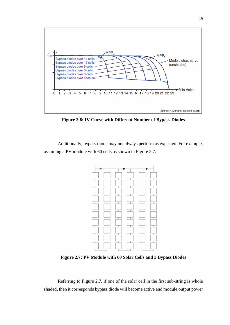
16
Figure 2.6: IV Curve with Different Number of Bypass Diodes
Additionally, bypass diode may not always perform as expected. For example,
assuming a PV module with 60 cells as shown in Figure 2.7.
Figure 2.7: PV Module with 60 Solar Cells and 3 Bypass Diodes
Referring to Figure 2.7, if one of the solar cell in the first sub-string is whole
shaded, then it corresponds bypass diode will become active and module output power
17
will drop by 1 / 3. Now, imagine if subjective shading happens to shade all the six solar
cells at the bottom row. This will lead to the activation of all bypass diodes and
eventually leads zero output, disabling the PV module.
Since bypass diodes alone is not sufficient to solve the partial shading losses
problem perfectly, new interconnection of solar cells is studied to increase the PV
module efficiency under various shading condition.
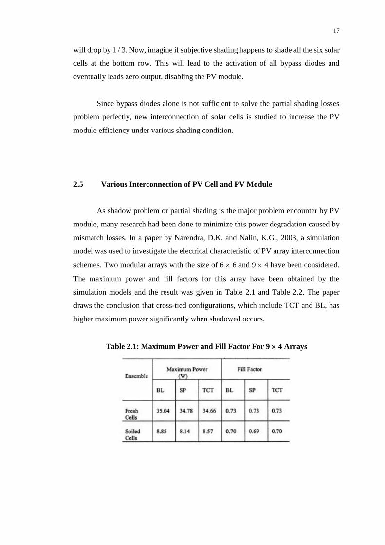
2.5 Various Interconnection of PV Cell and PV Module
As shadow problem or partial shading is the major problem encounter by PV
module, many research had been done to minimize this power degradation caused by
mismatch losses. In a paper by Narendra, D.K. and Nalin, K.G., 2003, a simulation
model was used to investigate the electrical characteristic of PV array interconnection
schemes. Two modular arrays with the size of 6 6 and 9 4 have been considered.
The maximum power and fill factors for this array have been obtained by the
simulation models and the result was given in Table 2.1 and Table 2.2. The paper
draws the conclusion that cross-tied configurations, which include TCT and BL, has
higher maximum power significantly when shadowed occurs.
Table 2.1: Maximum Power and Fill Factor For 9 4 Arrays
18
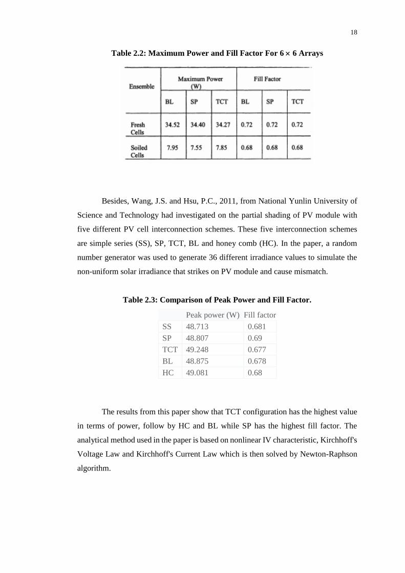
Table 2.2: Maximum Power and Fill Factor For 6 6 Arrays
Besides, Wang, J.S. and Hsu, P.C., 2011, from National Yunlin University of
Science and Technology had investigated on the partial shading of PV module with
five different PV cell interconnection schemes. These five interconnection schemes
are simple series (SS), SP, TCT, BL and honey comb (HC). In the paper, a random
number generator was used to generate 36 different irradiance values to simulate the
non-uniform solar irradiance that strikes on PV module and cause mismatch.
Table 2.3: Comparison of Peak Power and Fill Factor.
Peak power (W) Fill factor
SS 48.713 0.681
SP 48.807 0.69
TCT 49.248 0.677
BL 48.875 0.678
HC 49.081 0.68
The results from this paper show that TCT configuration has the highest value
in terms of power, follow by HC and BL while SP has the highest fill factor. The
analytical method used in the paper is based on nonlinear IV characteristic, Kirchhoff's
Voltage Law and Kirchhoff's Current Law which is then solved by Newton-Raphson
algorithm.

CHAPTER 3
3 METHODOLOGY
3.1 Overview
In this chapter, the method of study and implementation will be clarify and explain.
The main focus for this project is to study the different type of shading effect on the
solar cell operation and thus implement various interconnections of solar cells to
increase the efficiency of the PV panel. The methodology of the project is summarized
and presented as shown in Figure 3.1. The rough idea of each individual process block
will be explained below while the details of it will be discuss in several sub chapter.
Literature
ReviewDevelopment of
Data Logger
Soldering Solar
Panel
Data
CollectionData Analysis
Making
Conclusion
Figure 3.1: Flowchart of the Project

20
At the early stage of the project, literature review is done to gain information
and identify similar work that had been done by others engineer within the same area.
In addition, it allows me to compare and critique previous findings as so to suggest
further studies. All the information obtained for this project is from article, journal,
conference paper, textbook, internet, advice from senior engineers and guideline from
lecturer.
After the information gathered is sufficient and studied, the project move on to
the next stage which is the developing of data logger. The data logger are used to
collect data from the solar panels and record it directly into a SD card. The data
recorded are voltage, current and power. This data logger can be achieved by using an
Arduino Mega 2560 together with an Adafruit data logging shield. The details of the
data logger will be discuss further at section 3.2.
Next, the project continues to construct solar panel with three different
interconnection schemes. Three solar panels are constructed with different solar cell
interconnection schemes. The type of solar cell used is presented as in section 3.3.2
and the details for each solar cell interconnection schemes is discuss in section 3.3.1.
The initial planning for the data collection is by using the data logger
constructed with Arduino. However, this data logger is not used at the end due to some
limitations which will be further discuss later. The data collection is then achieved by
using PVPM1000CX I-V-Curve tracer. To collect data, each of the solar panel is
exposed to the sunlight. The data are first collect under no shading condition, then
different type of possible shading condition were carried out to study the effects of it
on each of the solar panel. Hence, the impact for different type of shading on solar
panel was experimented in this stage by analysing the data collected. Additionally,
total power output from different solar panel with different interconnection schemes
are be studied and data analysis are be carried out. Section 3.4 will explain how the
data been collect and which type of shading is model in details.

21
3.2 Data Logger
The data logger is served to log the required data directly from the solar panel into a
SD card instead. This can save a lot of time as compared to recording data by using
hand. The data logger comprise of several components which are Arduino Mega 2560,
Adafruit data logging shield, 16 2 LCD, button, SD card, ACS712 Hall Effect current
sensor, potentiometers and resistors. The selection of the components for the data
logger plays an important roles to make sure the data logger can function properly as
expected and able to log the output from solar panel correctly into the SD card.
Selecting appropriate components with reasonable price is also important to ensure the
total cost of the entire project is within budget.
3.2.1 Arduino Mega 2560
According to the Arduino official website, Arduino is an open-source electronics
platform that based on easy to us software and hardware. An Arduino board is aim to
provides a simple microcontroller kit that is able to interact with the user easily. With
multiple sensors as the input, it allows Arduino board to control the physical world
surrounding.
In this experiment, Arduino Mega 2560 as shown in Figure 3.2 is used. Arduino
Mega 2560 is an ATmega2560 microcontroller based circuit board with the dimension
of 101.52 mm 53.3 mm. It has 54 digital I/O pins, 16 analog inputs, 4 UARTs, a
16MHz crystal oscillator, a USB connection, a power jack, an ICSP header, and a reset
button. Table 3.1 shows the specification of Arduino Mega 2560.

22
Figure 3.2: Arduino Mega 2560
Table 3.1: Specification of Arduino Mega 2560
Microcontroller ATmega2560
Operating Voltage 5 V
Input Voltage (recommended) 7-12 V
Input Voltage (limit) 6-20 V
Digital I/O Pins 54 (of which 15 provide PWM output)
Analog Input Pins 16
DC Current per I/O Pin 20 mA
DC Current for 3.3V Pin 50 mA
Flash Memory 256 KB of which 8 KB used by bootloader
SRAM 8 KB
EEPROM 4 KB
Clock Speed 16 MHz
Length 101.52 mm
Width 53.3 mm
Weight 37 g
23
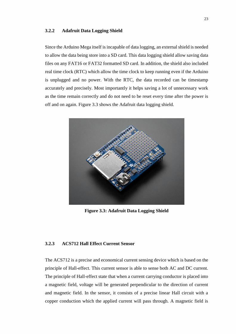
3.2.2 Adafruit Data Logging Shield
Since the Arduino Mega itself is incapable of data logging, an external shield is needed
to allow the data being store into a SD card. This data logging shield allow saving data
files on any FAT16 or FAT32 formatted SD card. In addition, the shield also included
real time clock (RTC) which allow the time clock to keep running even if the Arduino
is unplugged and no power. With the RTC, the data recorded can be timestamp
accurately and precisely. Most importantly it helps saving a lot of unnecessary work
as the time remain correctly and do not need to be reset every time after the power is
off and on again. Figure 3.3 shows the Adafruit data logging shield.
Figure 3.3: Adafruit Data Logging Shield
3.2.3 ACS712 Hall Effect Current Sensor
The ACS712 is a precise and economical current sensing device which is based on the
principle of Hall-effect. This current sensor is able to sense both AC and DC current.
The principle of Hall-effect state that when a current carrying conductor is placed into
a magnetic field, voltage will be generated perpendicular to the direction of current
and magnetic field. In the sensor, it consists of a precise linear Hall circuit with a
copper conduction which the applied current will pass through. A magnetic field is

24
then generated and being convert into proportional voltage by the Hall IC when current
applied. Figure 3.4 shows the ACS 712 current sensor and Table 3.2 shows the
specification of the sensor which is extracted from the datasheet.
Figure 3.4: ACS 712 Hall Effect Current Sensor
Table 3.2: Part of Specification of ACS712
3.3 Soldering Solar Panel
In this stage, several solar cells interconnection schemes that had been studied were
constructed to begin with the experiment. The solar cell interconnection schemes that

25
constructed includes series-parallel (SP), total cross tied (TCT) and bridge linked (BL).
As it is impossible to vary and change the interconnection of solar cells within an
existing PV panel, new PV panel was constructed or developed. In this project, several
small solar modules will play the role as solar cell and then being connect together to
form a big solar panel. The solar module being used will be shown at section 3.3.2.
3.3.1 Interconnection Scheme
A SP connection is the most common used connection in a PV panel. It is the most
simple connection scheme combining series and parallel connection. This type of
connection is commonly used to meet the load power requirements (Deshkar, et al.,
2015). However, from chapter two, we know that the connection scheme will gives
significant power drop when subject to shading. Next, it will be the TCT connection.
A TCT connection scheme is develop from the most basic SP connection by
connecting ties across each row of junctions. In other words, solar cells in row are
connected in parallel while solar cells in column are connected in series (Rani, Ilango
and Nagamani, 2013). Lastly will be BL scheme which is the derivation from bridge
rectifier pattern. Figure 3.5 shows all three interconnection schemes.
Figure 3.5: Diagram of SP, TCT and BL Interconnection Schemes

26
3.3.2 Solar Module
In the project, small solar module is used instead of raw solar cell. The reason for this
is that raw solar cell is not economically available and difficult to be handle. Raw solar
cell is normally being handle and connected by experience individual to avoid the risk
of damaging the cell. The small solar module that plays the role as solar cell in this
project is shown in the Figure 3.6 together with some its specification.
Figure 3.6: Solar Module
Table 3.3: Specification of the Solar Module
Maximum Power (Pmax) 0.12 Wp
Voltage at Maximum Power (Vmpp) 2 V
Current at Maximum Power (Impp) 60 mA
Bypass Diode 0
Dimension 40 40 mm
3.4 Data Collection
The next stage of the project is the data collection which involves measuring several
parameters such as Voc, Isc, Vmp, Imp, power output and irradiance level. An ideal
process of collecting data is to expose all three different interconnection scheme solar

27
panel side by side under the Sun at the same time so that they will have the data
collected under the exact same environment condition, irradiance level for example.
By doing so, we can save up a lot of time and effort while collecting data. Moreover,
we know that the irradiance level vary very fast, thus the data also have to be collect
in a very fast way before the irradiance level changes. In order to do that, a fast
performance data logger is needed so that sufficient data can be collected within a
small period of time.
As the result of that, the initial planning is to develop a data logger with
Arduino as it supports multiple inputs and able to perform fast. Additionally, this also
make sure the temperature remains unchanged as the data collection can be done in a
short period of time. However, due to some of the limitation, the data logger is not use.
Instead, PVPM1000CX I-V-Curve tracer was used for data logging.
The data was collected under several conditions in order to study the power
output for different interconnection scheme solar panel. The constant variable in the
experiment are irradiance level and temperature values while the manipulated
variables are the different type of shading condition. Different type of shading scenario
were carried out and model on all three solar panels. Cardboard was used to cover the
solar panel to simulate the partial shading effects. Several partial shading scenario was
performed such as shade horizontally, vertically, centre and etc. The data collection
for each type of shading on each interconnection schemes is estimated to be carry out
for 2 weeks. Multiple sets of data were obtained in order to get the average of the result
so that it is more precisely accurate.
3.4.1 Shading Pattern
There are several shading pattern done on the solar panel in order to model and
simulate all the possible shading that might happens. For example, a few solar cells at
the centre is to model a bird drop, leaves or dust. A whole column or whole row
shading is to simulate the shadow cause by nearby building or tree throughout the day.
The shading conditions that had been done are as follow:
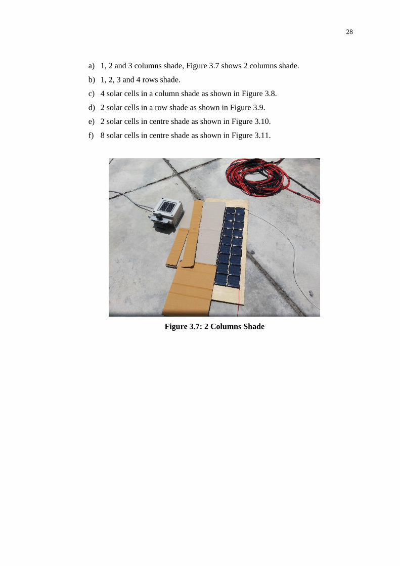
28
a) 1, 2 and 3 columns shade, Figure 3.7 shows 2 columns shade.
b) 1, 2, 3 and 4 rows shade.
c) 4 solar cells in a column shade as shown in Figure 3.8.
d) 2 solar cells in a row shade as shown in Figure 3.9.
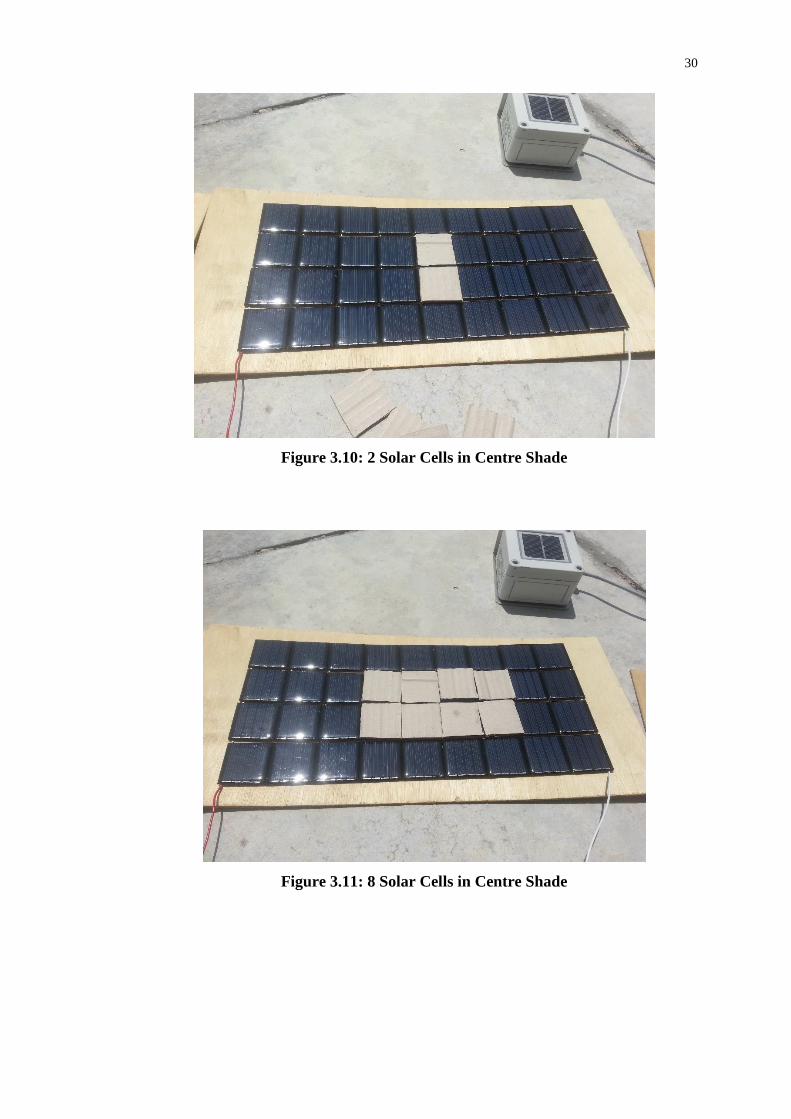
e) 2 solar cells in centre shade as shown in Figure 3.10.
f) 8 solar cells in centre shade as shown in Figure 3.11.
Figure 3.7: 2 Columns Shade

29
Figure 3.8: 4 Solar Cells in a Column Shade
Figure 3.9: 2 Solar Cells in a Row Shade
30
Figure 3.10: 2 Solar Cells in Centre Shade
Figure 3.11: 8 Solar Cells in Centre Shade

31
3.4.2 PVPM1000CX I-V-Curve Tracer
The PVPM is a device manufactured by a German company known as PV-Engineering
GmbH. The device is able to measure and trace the IV curve of solar module or strings.
Additionally, the device can measure and calculate the peak power Ppk, the Rs and Rp
from a single I-V-curve directly displaying the results and diagram on the internal
graphical LC display.
The PVPM1000CX is a portable measuring device with integrated battery
supply and battery charger in a durable and watertight plastic housing. The device can
also function independently from other devices with its own industrial miniature PC
and a high-contrast LCD TFT display. Moreover, it also allow data transfer to a
computer over a standard USB interface. From PC, further analysis of the measured
values can be done by using the compatible software installed. Figure 3.12 shows the
PVPM1000CX and Figure 3.13 shows part of its specification.
Figure 3.12: PVPM1000CX

32
Figure 3.13: Part of Specification of PVPM1000CX

33
3.5 Data Analysis
With all the data available, analysis was then carried out to study the performance of
each solar panel. From the data obtained, it is then used to plot IV curve and PV curve
so that the operating characteristic can be seen clearly and the maximum power output
point can be determined. From the graph, the working operation under partial shading
for different interconnection scheme is discuss.
For an effective ways of analysing data, one of the interconnection schemes
was set and use as the original reference so that the others two types of interconnection
can be compare with it. As the SP interconnection scheme is most commonly used, it
is set as the original references. By doing so, TCT and BL interconnection schemes
performance can be easily compare by referring to this original references.

CHAPTER 4
4 IMPLEMENTATION
4.1 Solar Panel
As discussed in chapter 3, three solar panels were constructed with three different
interconnection schemes which are Series Parallel, Total Cross Tied and Bridge Link
as shown in Figure 4.2. Each of the solar panel is made up by 36 small solar modules
with the configuration of 4 9. The solar panel was being connected with tabbing wire,
Figure 4.3. Figure 4.1 shows the front view of the solar panel.
Figure 4.1: Front View of the Solar Panel

35
(a) (b) (c)
Figure 4.2: (a) Series Parallel, (b) Total-Cross-Tied, and (c) Bridge-Link
Figure 4.3: Tabbing Wire
The solar modules was first being connected together in a string of nine pieces
and then parallel four strings to become a panel. Before connecting in parallel, each
string Voc and Isc is checked by multimeter to ensure the connection has good contact
and the solar modules is works. With the specification given for the solar module, we
36
can calculate the total voltage and current outputs for the solar panel under no shading
condition.
Given Vmpp = 2 V and Impp = 60 mA for one solar module, connecting nine in series
and four in parallel, each solar panel will have the output as,
𝑉𝑜𝑙𝑡𝑎𝑔𝑒 = 2 𝑉 × 9 = 18 𝑉
𝐶𝑢𝑟𝑟𝑒𝑛𝑡 = 60 𝑚𝐴 × 4 = 0.24 𝐴
𝑃𝑜𝑤𝑒𝑟 = 18 𝑉 × 0.24 𝐴 = 4.32 𝑊
4.2 Data Logger and IV Curve Tracer
The data logger is aim to record the output from the solar panel and thus it must be
able to measure the voltage, current and power values accurately and precisely. Others
than that, it also serve as an IV tracer. It can be achieved by implementing a
potentiometer as the load. By adjusting the resistance from lowest to highest, the
voltage output will change from minimum to maximum while the current output
change from maximum to minimum. By plotting out each point of the measured data,
an IV curve can be found. The greatest advantages of this data logger is that it can
collect multiple inputs at the same time, which other commercial IV tracer unable to
do so. Thus, the output from three solar panels can be collect and save simultaneously.
4.2.1 Voltage, Current and Power Measurement
Firstly, the Arduino measure the voltage value with its analog pin. As the analog pin
of Arduino is restricted to a maximum of 5 V, the voltage has to be scale down before
entering Arduino for measurement. In order to do that, voltage divider was used and
the circuit is designed in such a way that the output from it will be less than 5 V. From
the calculation above, the solar panel have a rated output voltage of 18 V so the voltage
divider circuit have to be able to scale down this voltage to less than 5 V.

37
The voltage divider have 2 resistors with the value of R1 = 47 kΩ and R2 = 10
kΩ. The values of these two resistors can be change as long as the ratio of it remains
the same. Notice that the value of R1 and R2 is high although the same ratio can be
achieve using other smaller value resistor. This is to eliminate and minimize the power
losses as there will be higher current flow when resistance is low. Figure 4.4 shows
the voltage divider circuit.
𝑉𝑜𝑢𝑡 = 𝑅2
𝑅1 + 𝑅2× 𝑉𝑠𝑜𝑙𝑎𝑟
𝑉𝑜𝑢𝑡 = 10 𝑘Ω
47 𝑘Ω + 10 𝑘Ω× 18 𝑉 = 3.16 V
Vout, To Arduino
R1,
47
k
R2,
10
k
Voltage from solar panel
Figure 4.4: Voltage Divider
Arduino have a built in 10 bit ADC that convert the signal from the analog
inputs to a corresponding digital values. A 10 bit resolution ADC will have 1024
unique values with respect to 5 V. In other word, each bit is representing 4.88 mV.

38
Thus, in order to measure the voltage accurately using Arduino, some calculation is
needed.
𝑉𝑜𝑢𝑡 = 𝐴0 ×5
1023
𝐴𝑐𝑡𝑢𝑎𝑙 𝑣𝑜𝑙𝑡𝑎𝑔𝑒 = 𝑉𝑜𝑢𝑡 ×57 𝑘Ω
10 𝑘Ω
Where A0 is the values read from the Arduino analog pin.
Next, the current measurement is achieved by using an ACS712 Hall Effect
current sensor. There are three types of ACS712 current sensor that has different
measurement range which are 5 A, 20 A and 30 A. The sensor used in this project is
20 A. From the datasheet, the sensor measure positive and negative 20 A which
correspond to its analog output of 100 mV / A. Also from the datasheet, the sensor will
have a 2.5 V offset which means that there will be a 2.5 V even no current is flowing
through. The calculation for current measurement is as follow,
𝑉𝑜𝑢𝑡 = 𝐴1 ×5
1023
𝑉𝑜𝑓𝑓𝑠𝑒𝑡 = 𝑉𝑜𝑢𝑡 − 2.5
𝐼 =𝑉𝑜𝑓𝑓𝑠𝑒𝑡
100
After getting voltage and current values, the power can be calculate by multiplying
voltage and current. Figure 4.5 shows the current sensing circuit.
Figure 4.5: Current Sensing Circuit

39
The complete circuit for the voltage and current measurement is shown as
Figure 4.6. Noted that this is not the complete circuit of data logger as this does not
include the connection of LCDs and button. Figure 4.7 shows the complete circuit of
the data logger.
Figure 4.6: Complete Sensing Circuit
Figure 4.7: Complete Circuit of Data Logger

40
4.2.2 Additional Features
Others than the expected function that a data logger should achieved which is logging
accurate voltage, current and power measurements into an SD card, this date logger
also comes with two extra features that worth mentioning. These two features are a
start / pause button and LCD display.
Originally, the data logger start logging the data into SD card at the moment it
is power on. Moreover, the data logger takes in data continuously with the desire
interval time set by the user, it is not possible to pause the data logger half way and
continues back from where it stop. In the application of measuring power from solar
panel, it is well aware that solar panel takes around 15 minutes to reach thermal
equilibrium. This means that the data output from the solar panel for the first 15
minutes might be not consistent and thus not convincing. This button comes in handy
at the time like this as the data logger will not start even after the power is turn on
unless the button is pressed. Further, the button also allow the user to pause the data
logging process at any time and resume it whenever the user want it. For example,
when the irradiance is too low for measurement, the user can press the button to pause
it and resume it back when the irradiance rise.
The next feature is the display of LCD. Although the data is being log into SD
card, it will still be better if there is a display to show the data instantaneously so that
the accuracy of the data can be monitor. With Arduino, we can monitor every data
output in a computer through a USB interface. However, the data logger is meant for
portable use and it will be troublesome to carry a computer around every time in order
to read the output instantaneously. With the aim of increasing the portability of the
data logger, LCD is added so that the data can be monitor even without a computer.
One of the advantages of using this LCD is that it is easy to use and customizable by
the user, so the user can display any data he wish. Figure 4.8 shows the different
display on the LCD.
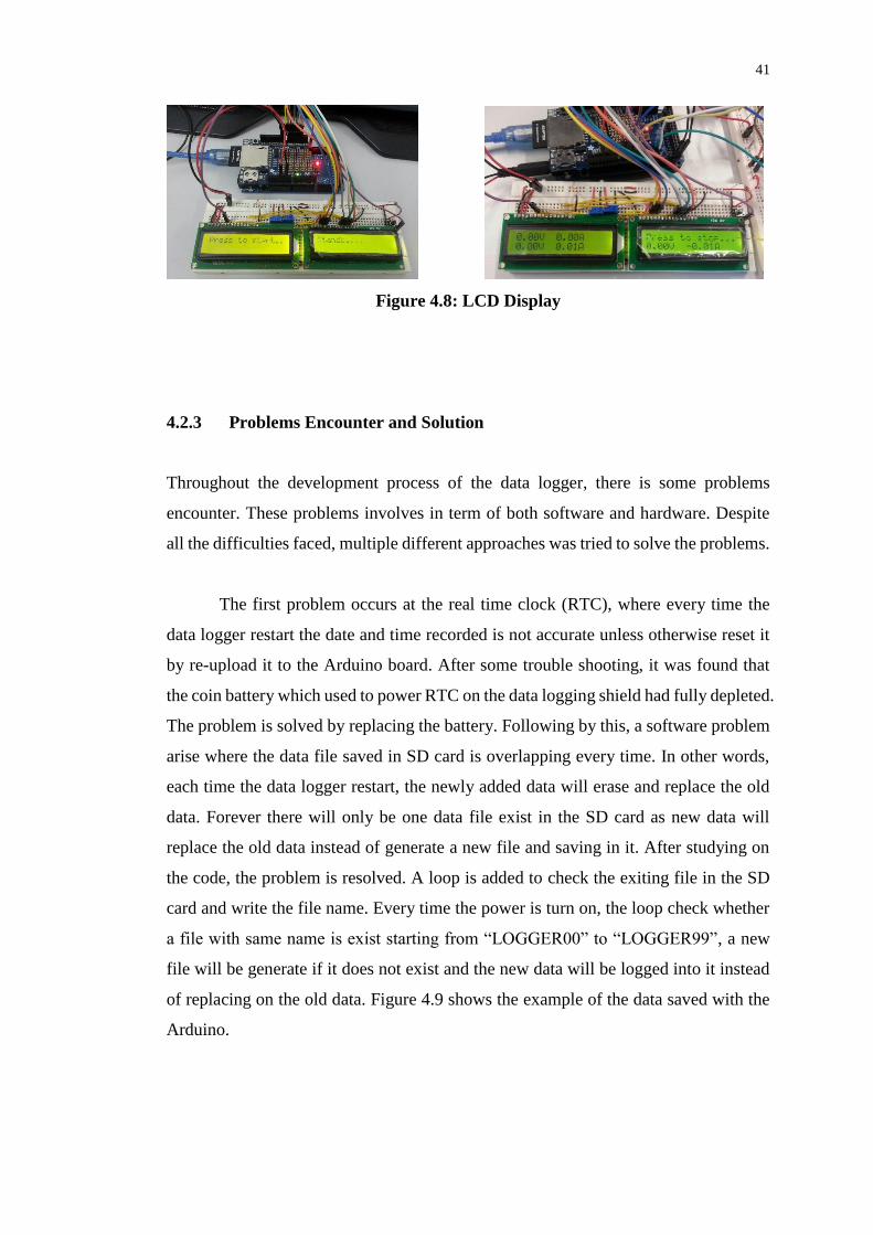
41
Figure 4.8: LCD Display
4.2.3 Problems Encounter and Solution
Throughout the development process of the data logger, there is some problems
encounter. These problems involves in term of both software and hardware. Despite
all the difficulties faced, multiple different approaches was tried to solve the problems.
The first problem occurs at the real time clock (RTC), where every time the
data logger restart the date and time recorded is not accurate unless otherwise reset it
by re-upload it to the Arduino board. After some trouble shooting, it was found that
the coin battery which used to power RTC on the data logging shield had fully depleted.
The problem is solved by replacing the battery. Following by this, a software problem
arise where the data file saved in SD card is overlapping every time. In other words,
each time the data logger restart, the newly added data will erase and replace the old
data. Forever there will only be one data file exist in the SD card as new data will
replace the old data instead of generate a new file and saving in it. After studying on
the code, the problem is resolved. A loop is added to check the exiting file in the SD
card and write the file name. Every time the power is turn on, the loop check whether
a file with same name is exist starting from “LOGGER00” to “LOGGER99”, a new
file will be generate if it does not exist and the new data will be logged into it instead
of replacing on the old data. Figure 4.9 shows the example of the data saved with the
Arduino.

42
Figure 4.9: Logged Data by Arduino Data Logger
Others than the software problem, the circuit also faced some problem which
the measured values is not precise and fluctuated particularly for current. After the
circuit was done assembly, the measurement accuracy was tested by supplying a
constant 5 V 3 A. It was found that the current measurement was not stable and keep
“jumping” around. After some deeper studied on the ACS712 current sensor and
troubleshooting, it was able to identify that the cause of this is the unstable input
voltage for the current sensor. When the input voltage is not stable, it cause the
references voltage and the offset value to oscillate. In the circuit, a single 5 V power
supply is used to power two LCDs and three ACS712 currents sensor splitting on 2
different breadboards, which is the main reason of unstable input voltage. The problem
is then resolve by supplying the current sensor an independent constant 5 V power
supply.
The last problem which is also the most critical problem arise when the IV
curve was plotted from the data collected. From the curve, it is obvious that all the
collected data are concentrated at the two ends of the graph, there is only less than 3
points at others part of the graph. Noted that the maximum current output for a solar
panel is 0.24 A as calculated from section 4.1 and the ACS712 current sensor used is
20 A. From here we can make the assumption that the 20 A current sensor sensitivity
is not precise enough for small current variation which is from 0 to 0.24 A. The
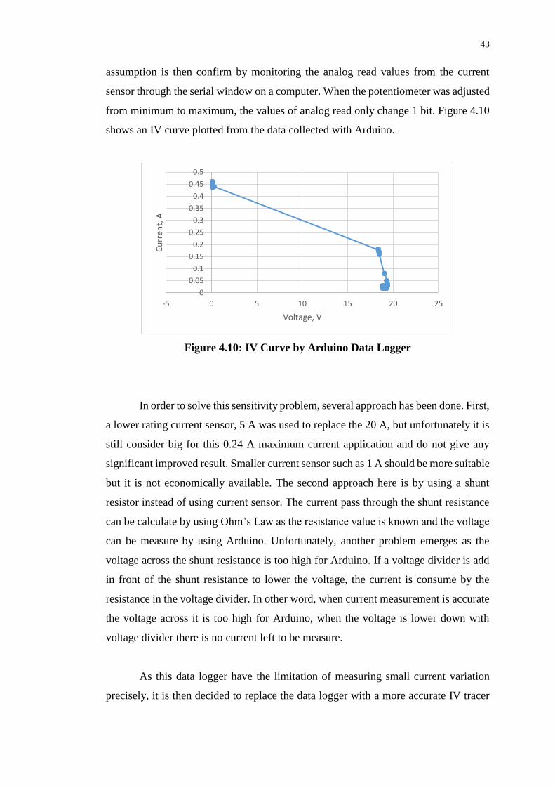
43
assumption is then confirm by monitoring the analog read values from the current
sensor through the serial window on a computer. When the potentiometer was adjusted
from minimum to maximum, the values of analog read only change 1 bit. Figure 4.10
shows an IV curve plotted from the data collected with Arduino.
Figure 4.10: IV Curve by Arduino Data Logger
In order to solve this sensitivity problem, several approach has been done. First,
a lower rating current sensor, 5 A was used to replace the 20 A, but unfortunately it is
still consider big for this 0.24 A maximum current application and do not give any
significant improved result. Smaller current sensor such as 1 A should be more suitable
but it is not economically available. The second approach here is by using a shunt
resistor instead of using current sensor. The current pass through the shunt resistance
can be calculate by using Ohm’s Law as the resistance value is known and the voltage
can be measure by using Arduino. Unfortunately, another problem emerges as the
voltage across the shunt resistance is too high for Arduino. If a voltage divider is add
in front of the shunt resistance to lower the voltage, the current is consume by the
resistance in the voltage divider. In other word, when current measurement is accurate
the voltage across it is too high for Arduino, when the voltage is lower down with
voltage divider there is no current left to be measure.
As this data logger have the limitation of measuring small current variation
precisely, it is then decided to replace the data logger with a more accurate IV tracer
0
0.05
0.1
0.15
0.2
0.25
0.3
0.35
0.4
0.45
0.5
-5 0 5 10 15 20 25
Cu
rren
t, A
Voltage, V

44
for data collection process, which is PVPM1000CX IV Curve Tracer. For higher
current, the data logger is working fine and able to give accurate measurement as was
tested in the lab. However, for small current application, some modification and
improvement can be done such as using more suitable current sensor values or use a
16 bit ADC instead of the Arduino built in 10 bit ADC.

CHAPTER 5
5 Results and Discussions
In this chapter, all the data collected is plot in IV curve and PV to study the
performance of each of the solar panel under the partial shading condition. Each graph
consists of three series of data from three different solar panel so that the differences
between them can be see more clearly. However, some of the graphs might only consist
one type of solar panel but with different partial shading pattern. The partial shading
pattern is as discussed in section 3.4.1.
First of all, it is clear that under no shading condition, three solar panel will
have the same total power output with same irradiance condition. Figure 5.1 and Figure
5.2 prove that the theory is correct as all the three solar panels have identical IV curve
and PV curve. The Voc is 18.9 V and the Isc is 0.35 A under the irradiance of 920 W /
m2, the power output is 4.4 W.
Figure 5.1: IV Curve for No Shading
-0.05
0
0.05
0.1
0.15
0.2
0.25
0.3
0.35
0.4
0 5 10 15 20
Cu
rren
t, A
Voltage, V
SP
TCT
BL

46
Figure 5.2: PV Curve for No Shading
When there is a whole column being shaded, the Isc drop to 0.26 A but the
voltage only slightly decrease and remains almost the same for all three types of solar
panels as shown in Figure 5.3. Noted that the TCT have slightly higher Isc compare to
the others two, however this is not significant enough to increase total power output.
The power output is 3.4 W when a column is being shaded as shown in Figure 5.4.
Figure 5.3: IV Curve for 1 Columns Shading
-1
0
1
2
3
4
5
0 5 10 15 20
Po
wer
, P
Voltage, V
SP
TCT
BL
-0.05
0
0.05
0.1
0.15
0.2
0.25
0.3
0 5 10 15 20
Cu
rren
t, A
Voltage, V
SP
TCT
BL

47
Figure 5.4: PV Curve for 1 Columns Shading
Moving on to 2 column shading, at this time, half of the solar cells was shaded
vertically. As current is add up for every strings connect in parallel, when two out of
four of the string was shaded, the Isc also drop by half to 0.17 A only. The Voc is now
18 V, compare to non-shaded 18.9 V, it is still consider high as total voltage output is
the sum from series connection. Thus, shading the whole column will not affect the
voltage output very much. The power output at this shading condition is 2.2 W. Figure
5.5 and Figure 5.6 shows the IV curve and PV curve respectively.
Figure 5.5: IV Curve for 2 Columns Shading
-0.5
0
0.5
1
1.5
2
2.5
3
3.5
4
0 5 10 15 20
Po
wer
, W
Voltage, V
SP
TCT
BL
-0.05
0
0.05
0.1
0.15
0.2
0 5 10 15 20
Cu
rren
t, A
Voltage, V
SP
TCT
BL

48
Figure 5.6: PV Curve for 2 Columns Shading
When three columns was shaded out of four columns, there is some interesting
finding shows. From Figure 5.7 and Figure 5.8, SP have higher power output with
higher Voc and Isc compare to TCT and BL. The power output for SP is 2.1 W which
is higher a lot higher than 0.9 W from TCT and BL
Figure 5.7: IV Curve for 3 Columns Shading
-0.5
0
0.5
1
1.5
2
2.5
0 5 10 15 20
Po
wer
, W
Voltage, V
SP
TCT
BL
-0.05
0
0.05
0.1
0.15
0.2
0 5 10 15 20
Cu
rren
t, A
Voltage, V
SP
TCT
BL

49
Figure 5.8: PV Curve for 3 Columns Shading
Summing up the points, as more columns are being shaded, the power drop
more with the lower current output. However, for SP connection, the power output did
not further decrease even when the shading extend from two columns to three columns,
the power remains the same. Table 5.1 give a better illustration on the power output
for all three solar panels with the increasing of shading area. Figure 5.9 and Figure
5.10 shows the IV and PV curve respectively for TCT column shading.
Table 5.1: Power Output for Column Shading
Power, W
Shading
SP TCT BL
No shading 4.4 4.4 4.4
1 column 3.4 3.4 3.4
2 columns 2.1 2.1 2.1
3 columns 2.1 0.9 0.9
-0.5
0
0.5
1
1.5
2
2.5
0 5 10 15 20
Po
wer
, W
Voltage, V
SP
TCT
BL

50
Figure 5.9: IV Curve for TCT Columns Shading
Figure 5.10: PV Curve for TCT Columns Shading
After the shading in column was analysed, the analysis move on to the shading
for row. From the experiment, the results shows in Figure 5.11 and 5.12 justify that
when a whole row of the solar panel was shade, there is no power output at all. There
are total of nine rows in the solar panel, there will be no power output regardless of
which row is being shaded. Every solar cells in a string will have the same current
flowing through and this current sums up when connect parallel with another string.
-0.05
0
0.05
0.1
0.15
0.2
0.25
0.3
0.35
0.4
0 5 10 15 20
Cu
rren
t, A
Voltage, V
No Shade
1 Column
2 Column
3 Column
-1
0
1
2
3
4
5
6
0 5 10 15 20
Po
wer
, P
Voltage, V
No Shade
1 Column
2 Column
3 Column

51
When a whole row is being shaded, one solar cell from each strings will have very
high resistance and thus blocking the current flow in each of their particular string. As
a result of that, there will be no power output if any of the row is being shaded.
Figure 5.11: IV Curve for 1 Row Shading
Figure 5.12: PV Curve for 1 Row Shading
From the result, we know that when a whole column are being shaded, all three
types of solar panel will have the same power output reduction. Only when three
-0.01
-0.008
-0.006
-0.004
-0.002
0
0.002
0.004
0 5 10 15 20
Cu
rren
t, A
Voltage, V
SP
TCT
BL
-0.05
-0.04
-0.03
-0.02
-0.01
0
0.01
0 5 10 15 20
Po
wer
, W
Voltage, V
SP
TCT
BL

52
columns are shaded, TCT and BL have same power output but SP have higher. What
if only a few cells in a column was shaded instead of the whole column? From Figure
5.13 and 5.14, it is obvious that TCT will have the highest power output follow by BL
and lastly is SP. Noted that all three solar panels have same Voc but different Isc which
cause the difference power output. By increasing the number of cells shaded in a
column, the power output is lower and the output difference between each type of solar
panel is larger.
Figure 5.13: IV Curve for 4 Cells in a Column Shading
Figure 5.14: PV Curve for 4 Cells in a Column Shading
-0.05
0
0.05
0.1
0.15
0.2
0.25
0.3
0.35
0 5 10 15 20
Cu
rren
t, A
Voltage, V
SP
TCT
BL
-0.5
0
0.5
1
1.5
2
2.5
3
3.5
4
4.5
0 5 10 15 20
Po
wer
, W
Voltage, V
SP
TCT
BL

53
Next, the shading condition is that two cells in a row being shaded. When
whole row is being shaded, there will be no power output as there is no current flow,
but when only half row is being shaded, the Isc is 0.185 A which is almost half the Isc
when there is no shading, shown in Figure 5.15. Looking at the PV curve from Figure
5.16, TCT have the highest power output which is 3.05 W, BL have slightly lower
which is 2.8 W and SP have lowest of 2.3 W. From study, we know that the power
output will drop by half as two out of four cells in a row was being shaded. The SP PV
curve prove this as its power output is half of the power when there is no shading, 4.4
W. With TCT and BL connection, the power output can be increase by 32% and 21%
respectively.
Figure 5.15: IV Curve for 2 Cells in a Row Shading
-0.05
0
0.05
0.1
0.15
0.2
0.25
0 5 10 15 20 25
Cu
rren
t, A
Voltage, V
SP
TCT
BL
54
Figure 5.16: PV Curve for 2 Cells in a Row Shading
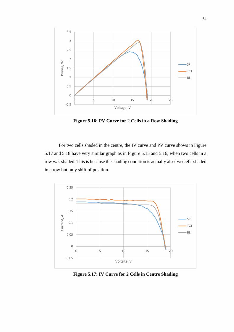
For two cells shaded in the centre, the IV curve and PV curve shows in Figure
5.17 and 5.18 have very similar graph as in Figure 5.15 and 5.16, when two cells in a
row was shaded. This is because the shading condition is actually also two cells shaded
in a row but only shift of position.
Figure 5.17: IV Curve for 2 Cells in Centre Shading
-0.5
0
0.5
1
1.5
2
2.5
3
3.5
0 5 10 15 20 25
Po
wer
, W
Voltage, V
SP
TCT
BL
-0.05
0
0.05
0.1
0.15
0.2
0.25
0 5 10 15 20
Cu
rren
t, A
Voltage, V
SP
TCT
BL

55
Figure 5.18: PV Curve for 2 Cells in Centre Shading
For eight cells shaded in centre, Figure 5.20 shows the power output for TCT
is 2.72 W, BL is 2.6 W and SP is 2.4 W. Figure 5.19 shows the IV curve. Generally,
TCT connection give highest power output under partial shading condition follow by
BL and SP. However, there is still some situation where TCT might not be the highest
as we can see from Figure 5.7 and figure 5.8. The reason that TCT have high power
output at most of the partial shading condition is that its interconnection between the
solar cells provide more pathway for the current to flow and bypass the shaded solar
cell.
-0.5
0
0.5
1
1.5
2
2.5
3
3.5
0 5 10 15 20
Po
wer
, W
Voltage, V
SP
TCT
BL
-0.05
0
0.05
0.1
0.15
0.2
0.25
0 5 10 15 20
Cu
rren
t, A
Voltage, V
SP
TCT
BL

56
Figure 5.19: IV Curve for 8 Cells in Centre Shading
Figure 5.20: PV Curve for 8 Cells in Centre Shading
-0.5
0
0.5
1
1.5
2
2.5
3
0 5 10 15 20
Po
wer
, W
Voltage, V
SP
TCT
BL
CHAPTER 6
6 CONCLUSION
6.1 Conclusion
In conclusion, all three project objectives have been met successfully at the end of the
project. From this project, the author was able learnt on various interconnection
schemes other than the commonly found Series Parallel (SP). These includes Total
Cross Tied (TCT), Bridge Link (BL), Honey Comb (HC) and etc.
Others than that, the author was able to construct three 4 9 solar panels with
the interconnection of SP, TCT and BL. This is achieved by connecting small solar
module with tabbing wire. Further, the effects of partial shading on different
interconnection solar panels were studied by monitoring the IV curve and PV curve. It
can be concluded that TCT and BL will have higher power output than the
conventional SP under partial shading condition. Among all the interconnection
schemes, TCT connection show the best performance under partial shading condition
as it has more current pathway for unshaded solar cell.
Besides meeting all the objectives, the author also achieved something as extra
and gain benefits from it. In this project, a simple IV tracer with the ability of logging
data was develop. Through the development of this IV tracer, the techniques to
measure voltage and current accurately by using Arduino was learnt. On top of that,
author was able to learnt how to logged data into an SD card and most importantly,
programming language was enhanced. This IV tracer and data logger is important to

58
this project as it has the advantage to collect multiple outputs from the solar panels
simultaneously, which cannot be done by others commercial IV tracer.
6.2 Future Implementation
6.2.1 Shading Patterns and Data Collection
From this project, I have learnt that different shading patterns give rise to different
performance on each solar panels. Thus, more shading patterns can be model and
simulate on the solar panel in order to have deeper understanding on how different
interconnection can increase the power output. Some suggested shading patterns are
shade diagonally, more solar cells shade in random and non-uniformly, shade half of
the solar cell and etc.
Throughout the project, it is clear that the even a small variation in solar
irradiance will affect the power output significantly. In this project, the data collection
is only done under the irradiance between 850 W / m2 to 950 W /m2. It is suggested
that more data can be collect under lower irradiance such as 600 W/ m2 or 200 W/ m2.
By doing so, someone can study and understand better at what irradiance level the
interconnection scheme will have the greatest effect and give most significant
increment at the total power output.
6.2.2 IV Tracer
Despite the IV tracer was able to measure voltage and current accurately and logged it
into an SD card, it has a limitation which is unable to detect a small changes of current.
For the IV tracer to have a better performance and trace the IV curve more accurately,
it must be able to detect the smallest current variation. In order to do that, smaller range
of current sensor can be used. Others than that, an ADC with higher bit resolution can

59
be used instead of using the built in ADC in Arduino which is only 10 bit. For example,
the Adafruit ADS1115 16 bit ADC.

60
REFERENCES
Berning, K., 2011. Design of stand-alone renewable power supply systems on Futuna
Island, VanuatuI. Sweden: Uppsala University.
Bulanyi, P. and Zhang, R., 2014. Shading analysis & improvement for distributed
residential grid-connected photovoltaics system.
Conserve Energy Future, 2015. Solar Energy. [online] Available at:
<http://www.conserve-energy-future.com/SolarEnergy.php> [Accessed 11 July
2015]
Deshkar, S.N., Dhale, S.B., Mukherjee, J.S., Babu, T.S. and Rajasekar, N., 2015. Solar
PV array reconfiguration under partial shading conditions for maximum power
extraction using genetic algorithm. Renewable and Sustainable Energy Reviews, 43,
pp 102 – 110.
Guo, S., Walsh, T.M., Aberle, A.G. and Peter, M., 2012. Analysing partial shading of
PV modules by circuit modelling. 38th IEEE Photovoltaic Specialists Conference
(PVSC). Austin, TX, 3-8 June 2012.
János, T. and Elza, K., 2008. Designing and operating passive solar systems.
Environmental Technology.
Kaushika, N.D. and Gautam, N.K., 2003. Energy Yield Simulations of Interconnected
Solar PV Arrays. IEEE Transaction on Energy Conversion, 18 (1), pp 127 – 134.
Mutoh, N., Ohno, M. and Inoue, T., 2006. A method for MPPT control while searching
for parameters corresponding to weather conditions for PV generation systems.
Industrial Electronics, 53 (4), pp. 1055 – 1065.
Pachpande, S.G. and Zope, P.H., 2012. Studying the effect of shading on Solar Panel
using MATLAB. International Journal of Science and Applied Information
Technology, 1 (2).
Petrone, G. and Paja, C.A.R., 2011. Modeling of photovoltaic fields in mismatched
conditions for energy yield evaluations. Electric Power System Research, 81 (4),
pp 1003 – 1013.
61
Picault, D., Raison, B., Bacha, S., Casa, J.D.L. and Aguilera, J., 2010. Forecasting
photovoltaic array power production subject to mismatch losses. Solar Energy, 84
(7), pp 1301 – 1309.
Rani, B.I., Ilango, G.S. and Nagamani, C., 2013. Enhanced power generation from PV
array under partial shading condition by shade dispersion using Su Do Ku
configuration. Sustainable Energy, 4 (3), pp 594 – 601.
Shukla, A., 2010. Optimization for generation scheduling with renewable energy
system. Degree. Thapar University.
Wang, Y.J. and Hsu, P.C., 2011. An investigation on partial shading of PV modules
with different connection configurations of PV cells. Energy, 36 (5), pp 3069 –
3078.

62
APPENDICES
APPENDIX A: Coding
#include <LiquidCrystal.h>
#include <SPI.h>
#include <SD.h>
#include <Wire.h>
#include "RTClib.h"
LiquidCrystal lcd1(8, 7, 9, 5, 4, 3, 2); //define pin for LCD 1
LiquidCrystal lcd2(8, 7, 6, 5, 4, 3, 2); //define pin for LCD 2
RTC_DS1307 RTC; //define the Real Time Clock object
File dataFile; //define data logging file
const int chipSelect = 10; //chip select 10 for Data Shield on Mega
byte logMode = 0; //to check logMode
const int button = 14;
float vsample1 = 0; // for voltage
float asample1 = 0; // for current
float vsample2 = 0;
float asample2 = 0;
float vsample3 = 0;
float asample3 = 0;
float voltage1 = 0.0;
float voltage2 = 0.0;
float voltage3 = 0.0;
float val1; // current callibration
float actualval1; // read the actual current from ACS 712
float amps1 = 0.0;
float val2;
float actualval2;
float amps2 = 0.0;
float val3;
float actualval3;
float amps3 = 0.0;
float watt1 = 0.0;
float watt2 = 0.0;
float watt3 = 0.0;
void setup()
Serial.begin(9600);
lcd1.begin(16, 2);
lcd2.begin(16, 2);

63
pinMode(button, INPUT); //button as input at pin 14
lcd1.print("Welcome!");
delay(1500);
lcd1.clear();
lcd2.print("Standby...");
Serial.print("Initializing SD card...");
lcd1.print("Initializing ");
lcd1.setCursor(0, 1);
lcd1.print("SD card...");
delay(1500);
lcd1.clear();
pinMode(53, OUTPUT); //set 53 as output for MEGA
//check if the card is present and initialized
while (!SD.begin(10, 11, 12, 13))
Serial.println("Card not insert or failed!");
lcd1.print("Card not insert");
lcd1.setCursor(0, 1);
lcd1.print("or failed!");
delay(1500);
lcd1.clear();
Serial.println("Card initialized!");
lcd1.print("Card ");
lcd1.setCursor(0, 1);
lcd1.print("initialized!");
delay(1500);
lcd1.clear();
//open file to log data
Serial.println("Opening file...");
lcd1.print("Opening File...");
delay(1500);
lcd1.clear();
char filename[] = "LOGGER00.CSV";
for (uint8_t i = 0; i < 100; i++)
filename[6] = i / 10 + '0';
filename[7] = i % 10 + '0';
if (!SD.exists(filename))
//only open a new file if it doesn't exist
dataFile = SD.open(filename, FILE_WRITE);
break; //leave the loop.
if (!dataFile)
Serial.println("Error opening file!");
lcd1.print("Error opening ");
lcd1.setCursor(0, 1);
lcd1.print("file!");
delay(1500);
while (1);
else
Serial.println("Logging to:");

64
Serial.println(filename);
lcd1.print("Logging to:");
lcd1.setCursor(0, 1);
lcd1.print(filename);
delay(1500);
lcd1.clear();
//kickstart the Real Time Clock
Wire.begin();
RTC.begin();
//print the header
dataFile.println("millis,Time,Voltage(SP),Current(SP),Power(SP),Voltage(TCT),Current(TCT),Power
(TCT),Voltage(BL),Current(BL),Power(BL)");
void loop()
if (digitalRead(button) == HIGH)
logMode = 1; //button pressed
else
logMode = 0; //button not pressed
if (logMode == 0)
lcd1.print("Press to start...");
lcd2.print("Standby...");
delay(100);
lcd1.clear();
lcd2.clear();
else
datalog(); //if pressed, go to datalog
void datalog()
logMode = 1;
do
long millisec = millis(); // calculate time in milisec
long time = millisec / 1000; // convert time to sec
for (int i = 0; i < 100; i++)
vsample1 += analogRead(A0); //read the voltage from the sensor
asample1 += analogRead(A1); //read the current from sensor
vsample2 += analogRead(A2);
asample2 += analogRead(A3);
vsample3 += analogRead(A8);
asample3 += analogRead(A9);
delay(1);
vsample1 = vsample1 / 100;
asample1 = asample1 / 100;
vsample2 = vsample2 / 100;
asample2 = asample2 / 100;
vsample3 = vsample3 / 100;
65
asample3 = asample3 / 100;
//voltage calculation
voltage1 = (((vsample1 * 5.03) / 1023) * 5.7);
voltage2 = (((vsample2 * 5.03) / 1023) * 5.7);
voltage3 = (((vsample3 * 5.03) / 1023) * 5.7);
//callibration, 3.25v is eqv 696 in A2 reading, multiply 2 to get actual voltage
//current calculation
Serial.println(asample1);
val1 = (asample1 / 1023) * 5000;
actualval1 = val1 - 2500; // offset voltage is 2.5v
amps1 = actualval1 / 100; // 100mv/A from data sheet
Serial.println(asample2);
val2 = (asample2 / 1023.0) * 4990;
actualval2 = val2 - 2500;
amps2 = actualval2 / 100;
Serial.println(asample3);
val3 = (asample3 / 1023.0) * 5030;
actualval3 = val3 - 2520;
amps3 = actualval3 / 100;
watt1 = voltage1 * amps1; // power=voltage*current
watt2 = voltage2 * amps2;
watt3 = voltage3 * amps3;
//DATA LOGGING
DateTime now;
dataFile.print(millisec);
dataFile.print(",");
Serial.print(millisec);
Serial.print(",");
// fetch the time
now = RTC.now();
// log time
dataFile.print(now.year(), DEC);
dataFile.print("/");
dataFile.print(now.month(), DEC);
dataFile.print("/");
dataFile.print(now.day(), DEC);
dataFile.print(" ");
dataFile.print(now.hour(), DEC);
dataFile.print(":");
dataFile.print(now.minute(), DEC);
dataFile.print(":");
dataFile.print(now.second(), DEC);
dataFile.print(",");
Serial.print(now.year(), DEC);
Serial.print("/");
Serial.print(now.month(), DEC);
Serial.print("/");
Serial.print(now.day(), DEC);
Serial.print(" ");
Serial.print(now.hour(), DEC);
Serial.print(":");
Serial.print(now.minute(), DEC);

66
Serial.print(":");
Serial.print(now.second(), DEC);
Serial.println("");
//log sensor values
dataFile.print(voltage1);
dataFile.print(",");
dataFile.print(amps1);
dataFile.print(",");
dataFile.print(watt1);
dataFile.print(",");
dataFile.print(voltage2);
dataFile.print(",");
dataFile.print(amps2);
dataFile.print(",");
dataFile.print(watt2);
dataFile.print(",");
dataFile.print(voltage3);
dataFile.print(",");
dataFile.print(amps3);
dataFile.print(",");
dataFile.print(watt3);
dataFile.println("");
//DISPLAY IN SERIAL MONITOR
Serial.print("VOLTAGE(SP) : ");
Serial.print(voltage1);
Serial.println(" Volt");
Serial.print("CURRENT(SP) :");
Serial.print(amps1);
Serial.println(" Amps");
Serial.print("VOLTAGE(TCT) : ");
Serial.print(voltage2);
Serial.println(" Volt");
Serial.print("CURRENT(TCT) :");
Serial.print(amps2);
Serial.println(" Amps");
Serial.print("VOLTAGE(BL) : ");
Serial.print(voltage3);
Serial.println(" Volt");
Serial.print("CURRENT(BL) :");
Serial.print(amps3);
Serial.println(" Amps");
//Serial.print("POWER :");
//Serial.print(watt);
//Serial.println("Watt");
//Serial.print("ENERGY CONSUMED :");
//Serial.print(energy);
//Serial.println("Watt-Hour");
Serial.println(""); // print the next sets of parameter after a blank line
//DISPLAY IN LCD
lcd1.setCursor(0, 0); // set the cursor at 1st col and 1st row
lcd1.print(voltage1);
lcd1.print("V ");
lcd1.print(amps1);
lcd1.print("A ");
lcd1.setCursor(0, 1);
lcd1.print(voltage2);
lcd1.print("V ");
67
lcd1.print(amps2);
lcd1.print("A ");
lcd2.setCursor(0, 0);
lcd2.print("Press to stop...");
lcd2.setCursor(0, 1); // set the cursor at 1st col and 2nd row
lcd2.print(voltage3);
lcd2.print("V ");
lcd2.print(amps3);
lcd2.print("A ");
dataFile.flush();
delay(1000);
if (digitalRead(button) == HIGH)
logMode = 0;
delay(500);
else
logMode = 1;
delay(500);
while (logMode == 1);