
Structure of Solids - WordPress.com of Solids Lecture Material Based on ... DENSITIES OF MATERIAL...
46
Structure of Solids Lecture Material Based on Introduction to Solid State Physics, John Wiley & Sons (C. Kittel, 1971) Power Point Presentation by Muchammad Chusnan Aprianto
Transcript of Structure of Solids - WordPress.com of Solids Lecture Material Based on ... DENSITIES OF MATERIAL...

Structure of
Solids
Lecture Material Based on
Introduction to Solid State Physics,
John Wiley & Sons (C. Kittel, 1971)
Power Point Presentation by
Muchammad Chusnan Aprianto

ISSUES TO ADDRESS...
• How do atoms assemble into solid structures?
• How does the density of a material depend on
its structure?
• When do material properties vary with the
sample orientation?

POLYCRYSTALLINE MATERIALS • ―Nuclei‖ form during solidification, each of which grows into crystals

• Dense, regular packing
Dense, regular-packed structures tend to have lower energy
ENERGY AND PACKING
• Non dense, random packing

SOME DEFINITIONS … • Lattice: 3D array of regularly
spaced points
• Crystalline material: atoms situated in a repeating 3D periodic array over large atomic distances
• Amorphous material: material with no such order
• Hard sphere representation: atoms denoted by hard, touching spheres
• Reduced sphere representation
• Unit cell: basic building block unit (such as a flooring tile) that repeats in space to create the crystal structure; it is usually a parallelepiped or prizm

• tend to be densely packed.
• have several reasons for dense packing:
-Typically, made of heavy element.
-Metallic bonding is not directional; i.e., no
restrictions as to the number and position of
nearest-neighbor atoms
-Nearest neighbor distances tend to be small in
order to lower bond energy.
• have the simplest crystal structures.
We will look at four such structures...
METALLIC CRYSTALS

• Cubic unit cell is 3D repeat unit
• Rare (only Po has this structure)
• Close-packed directions (directions along which atoms touch each other)
are cube edges. • Coordination # = 6
(# nearest neighbors)
(Courtesy P.M. Anderson)
SIMPLE CUBIC STRUCTURE (SC)

ATOMIC PACKING FACTOR
• Fill a box with hard spheres
– Packing factor = total volume of spheres in
box / volume of box
– Question: what is the maximum packing factor
you can expect?
• In crystalline materials:
– Atomic packing factor = total volume of atoms
in unit cell / volume of unit cell
– (as unit cell repeats in space)

• APF for a simple cubic structure = 0.52
ATOMIC PACKING FACTOR
contains 8 x 1/8 = 1 atom/unit cell
Adapted from Fig. 3.19,
Callister 6e.
Lattice constant
close-packed directions
a
R=0.5a

• Coordination # = 8
Adapted from Fig. 3.2,
Callister 6e. (Courtesy P.M. Anderson)
• Close packed directions are cube diagonals. --Note: All atoms are identical; the center atom is shaded
differently only for ease of viewing.
BODY CENTERED CUBIC
STRUCTURE (BCC)

aR
• APF for a body-centered cubic structure = p3/8 = 0.68
Unit cell contains: 1 + 8 x 1/8 = 2 atoms/unit cell
Adapted from
Fig. 3.2,
Callister 6e.
ATOMIC PACKING FACTOR: BCC
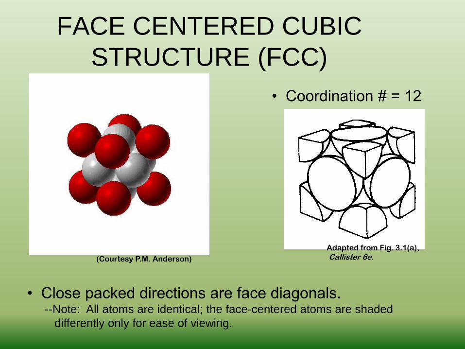
• Coordination # = 12
Adapted from Fig. 3.1(a),
Callister 6e. (Courtesy P.M. Anderson)
• Close packed directions are face diagonals. --Note: All atoms are identical; the face-centered atoms are shaded
differently only for ease of viewing.
FACE CENTERED CUBIC
STRUCTURE (FCC)

Unit cell contains: 6 x 1/2 + 8 x 1/8 = 4 atoms/unit cell
a
• APF for a body-centered cubic structure = p/(32) = 0.74
(best possible packing of identical spheres)
Adapted from
Fig. 3.1(a),
Callister 6e.
ATOMIC PACKING FACTOR: FCC

• ABCABC... Stacking Sequence
• FCC Unit Cell
FCC STACKING SEQUENCE
A sites
B sites
C sites
B B
B
BB
B BC C
CA
A
• 2D Projection

HEXAGONAL CLOSE-PACKED
STRUCTURE (HCP)
Ideally, c/a = 1.633 for close packing
However, in most metals, c/a ratio deviates from this value

• Coordination # = 12
• ABAB... Stacking Sequence
• APF = 0.74, for ideal c/a ratio of 1.633
• 3D Projection • 2D Projection
A sites
B sites
A sites
Adapted from Fig. 3.3,
Callister 6e.
HEXAGONAL CLOSE-PACKED
STRUCTURE (HCP)
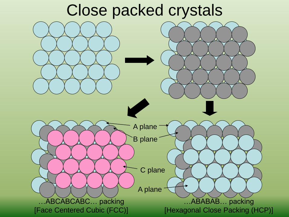
Close packed crystals
A plane
B plane
C plane
A plane
…ABCABCABC… packing
[Face Centered Cubic (FCC)]
…ABABAB… packing
[Hexagonal Close Packing (HCP)]

COMPARISON OF CRYSTAL
STRUCTURES
Crystal structure coordination # packing factor close packed directions
• Simple Cubic (SC) 6 0.52 cube edges
• Body Centered Cubic (BCC) 8 0.68 body diagonal
• Face Centered Cubic (FCC) 12 0.74 face diagonal
• Hexagonal Close Pack (HCP) 12 0.74 hexagonal side

THEORETICAL DENSITY, r
Density = mass/volume
mass = number of atoms per unit cell * mass of each atom
mass of each atom = atomic weight/avogadro’s number

Element Aluminum Argon Barium Beryllium Boron Bromine Cadmium Calcium Carbon Cesium Chlorine Chromium Cobalt Copper Flourine Gallium Germanium Gold Helium Hydrogen
Symbol Al Ar Ba Be B Br Cd Ca C Cs Cl Cr Co Cu F Ga Ge Au He H
At. Weight (amu) 26.98 39.95 137.33 9.012 10.81 79.90 112.41 40.08 12.011 132.91 35.45 52.00 58.93 63.55 19.00 69.72 72.59 196.97 4.003 1.008
Atomic radius (nm) 0.143 ------ 0.217 0.114 ------ ------ 0.149 0.197 0.071 0.265 ------ 0.125 0.125 0.128 ------ 0.122 0.122 0.144 ------ ------
Density
(g/cm3) 2.71 ------ 3.5 1.85 2.34 ------ 8.65 1.55 2.25 1.87 ------ 7.19 8.9 8.94 ------ 5.90 5.32 19.32 ------ ------
Adapted from
Table, "Charac-
teristics of
Selected
Elements",
inside front
cover,
Callister 6e.
Characteristics of Selected Elements at 20C

Example: Copper Data from Table inside front cover of Callister (see previous slide):
• crystal structure = FCC: 4 atoms/unit cell
• atomic weight = 63.55 g/mol (1 amu = 1 g/mol)
• atomic radius R = 0.128 nm (1 nm = 10 cm) -7
Compare to actual: rCu = 8.94 g/cm3Result: theoretical rCu = 8.89 g/cm3
THEORETICAL DENSITY, r

Why? Metals have... • close-packing
(metallic bonding)
• large atomic mass
Ceramics have... • less dense packing
(covalent bonding)
• often lighter elements
Polymers have... • poor packing
(often amorphous)
• lighter elements (C,H,O)
Composites have... • intermediate values Data from Table B1, Callister 6e.
DENSITIES OF MATERIAL CLASSES
r metals > r ceramic s > r polymer s

CRYSTAL SYSTEMS
• Based on shape of unit cell ignoring actual atomic locations
• Unit cell = 3-dimensional unit that repeats in space
• Unit cell geometry completely specified by a, b, c & a, b, g (lattice parameters or lattice constants)
• Seven possible combinations of a, b, c & a, b, g, resulting in seven crystal systems

CRYSTAL SYSTEMS

• Structure of NaCl
STRUCTURE OF OTHER SYSTEMS
(Courtesy P.M. Anderson)
• Structure of Carbon
Graphite Diamond

CRYSTAL STRUCTURES
• Plenty of crystal structures available at:
http://cst-www.nrl.navy.mil/lattice/
• Polymorphism
– Same compound occurring in more than one crystal
structure
• Allotropy
– Polymorphism in elemental solids (e.g., carbon)

CRYSTALLOGRAPHIC POINTS,
DIRECTIONS & PLANES • In crystalline materials, often necessary to specify points,
directions and planes within unit cell and in crystal lattice
• Three numbers (or indices) used to designate points, directions (lines) or planes, based on basic geometric notions
• The three indices are determined by placing the origin at one of the corners of the unit cell, and the coordinate axes along the unit cell edges

POINT COORDINATES • Any point within a unit cell specified as fractional
multiples of the unit cell edge lengths
• Position P specified as q r s; convention: coordinates not separated by commas or punctuation marks

EXAMPLE: POINT COORDINATES
• Locate the point (1/4 1 ½)
• Specify point coordinates for all atom
positions for a BCC unit cell
– Answer: 0 0 0, 1 0 0, 1 1 0, 0 1 0, ½ ½ ½,
0 0 1, 1 0 1, 1 1 1, 0 1 1

CRYSTALLOGRAPHIC DIRECTIONS
• Defined as line between two points: a vector
• Steps for finding the 3 indices denoting a direction
– Determine the point positions of a beginning point (X1 Y1 Z1)
and a ending point (X2 Y2 Z2) for direction, in terms of unit cell
edges
– Calculate difference between ending and starting point
– Multiply the differences by a common constant to convert them
to the smallest possible integers u, v, w
– The three indices are not separated by commas and are
enclosed in square brackets: [uvw]
– If any of the indices is negative, a bar is placed in top of that
index

COMMON DIRECTIONS

EXAMPLES: DIRECTIONS
• Draw a [1,-1,0] direction within a cubic unit cell
• Determine the indices for this direction
– Answer: [120]

CRYSTALLOGRAPHIC PLANES
• Crystallographic planes specified by 3 Miller indices as (hkl)
• Procedure for determining h,k and l: – If plane passes through origin, translate
plane or choose new origin
– Determine intercepts of planes on each of the axes in terms of unit cell edge lengths (lattice parameters). Note: if plane has no intercept to an axis (i.e., it is parallel to that axis), intercept is infinity (½ ¼ ½)
– Determine reciprocal of the three intercepts (2 4 2)
– If necessary, multiply these three numbers by a common factor which converts all the reciprocals to small integers (1 2 1)
– The three indices are not separated by commas and are enclosed in curved brackets: (hkl) (121)
– If any of the indices is negative, a bar is placed in top of that index
1/2
1/2
1/4
(1 2 1)X
Y
Z

THREE IMPORTANT CRYSTAL
PLANES
( 1 0 0) (1 1 1)(1 1 0)

THREE IMPORTANT CRYSTAL
PLANES
• Parallel planes are equivalent

EXAMPLE: CRYSTAL PLANES
• Construct a (0,-1,1) plane

FCC & BCC CRYSTAL PLANES
• Consider (110) plane
• Atomic packing different in the two cases
• Family of planes: all planes that are
crystallographically equivalent—that is having the
same atomic packing, indicated as {hkl}
– For example, {100} includes (100), (010), (001) planes
– {110} includes (110), (101), (011), etc.

LINEAR & PLANAR DENSITIES
• Linear density (LD) = number of atoms centered on a direction vector / length of direction vector – LD (110) = 2 atoms/(4R) = 1/(2R)
• Planar density (PD) = number of atoms centered on a plane / area of plane – PD (110) = 2 atoms /
[(4R)(2R2)] = 2 atoms / (8R22) = 1/(4R22)
• LD and PD are important considerations during deformation and ―slip‖; planes tend to slip or slide along planes with high PD along directions with high LD

• Some engineering applications require single crystals:
• Crystal properties reveal features
of atomic structure.
(Courtesy P.M. Anderson)
--Ex: Certain crystal planes in quartz
fracture more easily than others.
--diamond single
crystals for abrasives
--turbine blades
Fig. 8.30(c), Callister 6e.
(Fig. 8.30(c) courtesy
of Pratt and Whitney). (Courtesy Martin Deakins,
GE Superabrasives,
Worthington, OH. Used with
permission.)
CRYSTALS AS BUILDING BLOCKS • Single crystal: when the periodic and repeated
arrangement of atoms is perfect and extends throughout
the entirety of the specimen

POLYCRYSTALLINE MATERIALS • ―Nuclei‖ form during solidification, each of which grows into crystals

• Most engineering materials are polycrystals.
• Nb-Hf-W plate with an electron beam weld.
• Each "grain" is a single crystal.
• If crystals are randomly oriented, overall component properties are not directional.
• Crystal sizes typ. range from 1 nm to 2 cm
(i.e., from a few to millions of atomic layers).
Adapted from Fig. K,
color inset pages of
Callister 6e.
(Fig. K is courtesy of
Paul E. Danielson,
Teledyne Wah Chang
Albany)
1 mm
POLYCRYSTALS

• Single Crystals
-Properties vary with
direction: anisotropic.
-Example: the modulus
of elasticity (E) in BCC iron:
• Polycrystals
-Properties may/may not
vary with direction.
-If grains are randomly
oriented: isotropic.
(Epoly iron = 210 GPa)
-If grains are textured,
anisotropic.
200 mm
Data from Table 3.3,
Callister 6e.
(Source of data is R.W.
Hertzberg, Deformation
and Fracture Mechanics
of Engineering
Materials, 3rd ed., John
Wiley and Sons, 1989.)
Adapted from Fig.
4.12(b), Callister 6e.
(Fig. 4.12(b) is courtesy
of L.C. Smith and C.
Brady, the National
Bureau of Standards,
Washington, DC [now
the National Institute of
Standards and
Technology,
Gaithersburg, MD].)
SINGLE VS POLYCRYSTALS

• atoms pack in periodic, 3D arrays
• typical of:
Crystalline materials...
-metals
-many ceramics
-some polymers
• atoms have no periodic packing
• occurs for:
Noncrystalline materials...
-complex structures
-rapid cooling
crystalline SiO2
noncrystalline SiO2 "Amorphous" = Noncrystalline Adapted from Fig. 3.18(b),
Callister 6e.
Adapted from Fig. 3.18(a),
Callister 6e.
AMORPHOUS MATERIALS

• Incoming X-rays diffract from crystal planes, following
Braggs law: nl = 2dsin(q)
• Measurement of:
Critical angles, qc,
for X-rays provide
atomic spacing, d.
Adapted from Fig. 3.2W,
Callister 6e.
X-RAYS TO CONFIRM CRYSTAL STRUCTURE

• Atoms can be arranged and imaged!
Carbon monoxide
molecules arranged
on a platinum (111)
surface.
Photos produced from
the work of C.P. Lutz,
Zeppenfeld, and D.M.
Eigler. Reprinted with
permission from
International Business
Machines Corporation,
copyright 1995.
Iron atoms arranged
on a copper (111)
surface. These Kanji
characters represent
the word ―atom‖.
SCANNING TUNNELING
MICROSCOPY

• Atoms may assemble into crystalline,
polycrystalline or amorphous structures.
• We can predict the density of a material,
provided we know the atomic weight, atomic
radius, and crystal geometry (e.g., FCC,
BCC, HCP).
• Material properties generally vary with single
crystal orientation (i.e., they are anisotropic),
but properties are generally non-directional
(i.e., they are isotropic) in polycrystals with
randomly oriented grains.
SUMMARY


