STRUCTURAL STUDIES ON INDIUM OXIDE, TIN...
25
CHAPTER V STRUCTURAL STUDIES ON INDIUM OXIDE, TIN OXIDE AND INDIUM TIN OXIDE THIN FILMS
Transcript of STRUCTURAL STUDIES ON INDIUM OXIDE, TIN...
CHAPTER V
STRUCTURAL STUDIES ON INDIUM OXIDE, TIN OXIDE AND INDIUM
T IN OXIDE THIN FILMS

5.1 Introduction
The applications of indiun oxide, tin oxide and indium tin oxide have
been remarkable in the field of gas sensors, '" where structure and particle
size are important parameters for high sensitivity and rapid response. In this
chapter the structural properties of indium oxide, tin oxide and indium tin
oxide films are dealt with.
It is known that indium oxide crystallizes in two different structures
as body centered cubic and hexagonal. The body centered cubic structure
is a bixbyite Mn203 type, also called C-type rare earth oxide structure. The
unit cell consists of 16 mol~?cules, i.e., 80 atoms, resulting in a rather
complex structure. This phase is obtained at a low or normal pressure.
The hexagonal type is a high-pressure type phase obtained at 68 Kbar
and at a temperature 800- l f i 00~~ . The structure is of the corundum, or
CCAl203 type, and has 6 molecules per unit cell.
There are two crystallographically non-equivalent indium atoms but
only one type of oxygen atom. The indium is six-fold coordinated and
oxygen is four-fold coordinated. The oxygen atoms around In (1) are
equidistant (In-0 = 0.21 8 nm) and lie nearly at the comers of a cube with
two body diagonally opposite corners unoccupied. In (2) is also
surrounded by six oxygen atoms nearly at the corners of the cube, but
with two face-diagonally opposite corners unoccupied. In this polyhedron
the six In-0 distances have, three different values: 0.213nm, 0.219 nm and
0.223 nm.
Tin oxide (Sn02) single crystal has tetragonal rutile structure with
space group ~ ' ~ ~ t , (P42/mnm). It is a non-symmorphic crystal with two
formula units per unit cell. The unit cell contains six atoms, two tin and
four oxygen. The coordination is 6:3. The oxygen atoms are placed
approximately at the corners of a regular octahedron, and tin atoms are
located approximately at the colFners of an equilateral triang~e.~ The lattice
parameters are a0 = 0.473 nm and co= 0.3186 nm.
The structure of IT0 is essentially tin doped indium oxide, which is
known to crystallize in body centered cubic and hexagonal structures.
When small amount of tin is added to indium oxide all the tin atoms
enter substitutionally in the cation sub lattice. The tin doping has been
observed to induce a change in the lattice constant. Some authors 6-8
obtained 'a' higher than 'a6 of undoped indium oxide, which may suggest
3+ . the incorporation of larger ~ n " ions at either In s~te substitutionally or at
interstitial positions. Agnihotri et a/..' observed a reduction of the lattice
constant with increase in tin concentration in IT0 films. Such a lattice
contraction indicates the replacement of ln3+ ion by sn4' ions that are
smaller. Mossbauer results "' have shown that tin in good quality IT0
films are either in sn4+ state or in Sn '+ state. Thilakan et a/." observed a
change in preferred orientation between (222) and (400) planes when
deposition rate is increased.
5.2 Indium Oxide
Indium oxide thin films have been prepared using the vacuum
coating unit and a tantalum boat as described in Chapter 4 (Section 4.4).
The samples are prepared in an oxygen partial pressure of 3x10'~ mbar at
substrate temperatures 125, .75, 200 and 225OC. The thickness of the
films are 500nm each. XRD spectrum of these samples are recorded
using X-ray diffractometer (Philips - PW 3710) as described in chapter 2
(section 2.23). The radiation used is CuKa and the operating potential is
25KV and current 10mA. The scanning rate is 1°/minute.
Fig 5.1 to 5.4 gives the XRD pattern of the indium oxide thin films
deposited at 125O~, 175OC, 2 0 0 ' ~ and 2 2 5 ' ~ and annealed for 30
minutes at 250'~. At 175'C, the peak obtained at 20 = 30.5' is examined
and identified as the reflection from (222) plane of indium oxide using
ASTM (American Society fcr Testing Materials) data card. The other
peaks are identified and are given in Table 5.1.

Fig. 5.1 XRD pattern of indiurnoxide thin film deposited at substrate temperature 125'~.

LR -t
Fig. 5.2 XRD pattern of indium oxide thin film deposited at substrate temperature 175'~.

28 -, Fig. 5.3 XRD pattern indium oxide thin film deposited at a substrate
temperature200~C.
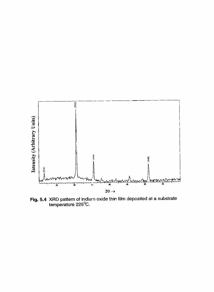
Fig. 5.4 XRD pattern of indiurn oxide thin film deposited at a substrate temperature 225OC.
Table 5.1 The calculated values of d and the ASTM standard values of d for indium oxide film deposited at 1 7 5 ' ~ and annealed at 2 5 0 ' ~ for 30 minutes
The grain size of the films are determined from the Full Width at
20
21.5
30.5
35.46
45.7
50.98
Half Maximum (FWHM) intensity of the X-ray peaks using Scherrer's
formu~a.'~
Where h = 0.154056 nm, 1 6 ~ = B-b, where B is the width of peak at an 2
angle 28 at half maximum intensity and b is the effect of the instrument as
Inter planar spacing (d)
determined from the broadening of the monocrystalline silicon diffraction
ulo
14
100
30
0
35
C:alculated (nm)
12.92 4.12
100 2.92
23.7 2.53
6.0 1.98
29.5 1.79
line. The values of the grain :size are given in Table 5.2.
hkl
21 1
222
400
431
440
ASTM (nm)
4.13
2.921
2.529
1.984
1.788

Table 5.2 The grain size of Indium oxide thin films deposited at various substrate temperatures
Grain size (nm) 1 -+r
The grain size is found to increase with increase in substrate
temperature. Goswami and 3oswami l3 and Burns l4 report that the
vacuum evaporated indium oxide films may dissociate to species like InO,
In or 02.
As observed, a preferential orientation (222) for indium oxide has
been obtained by Sundaram ttnd Bhagavat l5 and Weng et a1.I6 It is also
reported that the preferred olentation depends on film thickness17 and
deposition conditions. 18
5.3 Tin Oxide
Thin films of tin oxidct have been prepared using the thermal
evaporation technique. The procedure for the preparation is described in
Chapter 4 (Section 4.5). Thickness of the sample is 500 nm each. XRD
spectra of the samples have heen recorded using the Philips (PW -3710)
X-ray diffractometer.
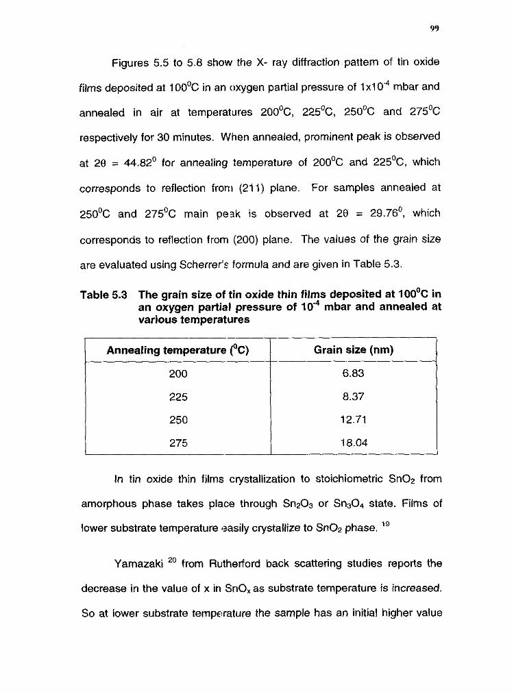
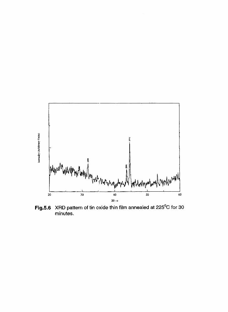
Figures 5.5 to 5.8 show the X- ray diffraction pattern of tin oxide
films deposited at 1 0 0 ~ ~ in an oxygen partial pressure of 1x10.~ mbar and
annealed in air at temperatures 200°c, 225'~, 250% and 275OC
respectively for 30 minutes. When annealed, prominent peak is observed
at 28 = 44.82' for annealing temperature of 200% and 225Oc, which
corresponds to reflection from (21 1) plane. For samples annealed at
250°C and 275% main peak is observed at 29 = 29.76', which
corresponds to reflection from (200) plane. The values of the grain size
are evaluated using Scherrer's formula and are given in Table 5.3.
Table 5.3 The grain size of tin oxide thin films deposited at 1 0 0 ~ ~ in an oxygen partial pressure of lo4 mbar and annealed at various temperatures
Annealing temperature (OC) Grain size (nm)
In tin oxide thin films crystallization to stoichiometric Sn02 from
amorphous phase takes place through Sn203 or Sn304 state. Films of
lower substrate temperature easily crystallize to Sn02 phase. 19
Yamazaki 20 from Rutherford back scattering studies reports the
decrease in the value of x in SnO, as substrate temperature is increased.
So at lower substrate temperature the sample has an initial higher value
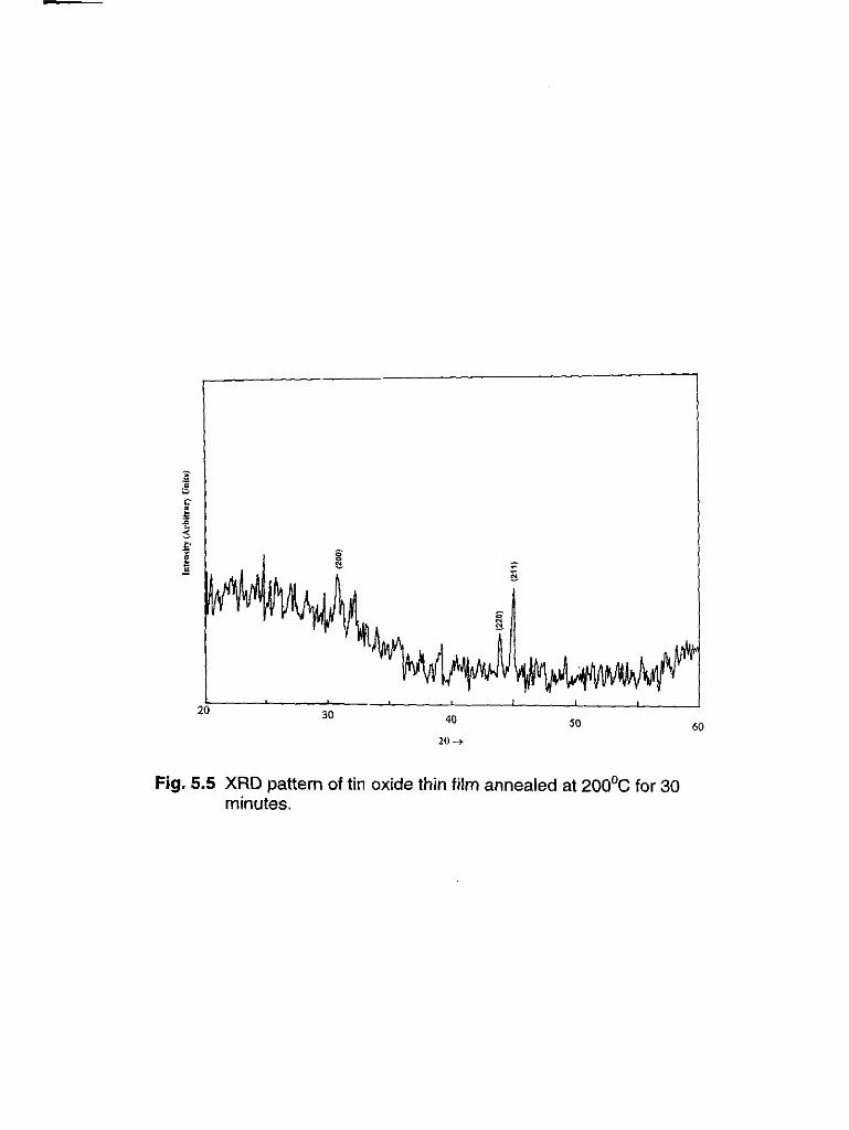
Fig. 5.5 XRD pattern of tin oxide thin film annealed at 200'~ for 30 minutes.
a 3 F; b B a .- : g n -
20 30 40 50 60
20 -f
Fig.5.6 XRD pattern of tin oxide thin film annealed at 225'~ for 30 minutes.
Fig.5.7 XRD pattern of tin oxide thin film annealed at 2 5 0 ' ~ for 30 minutes.
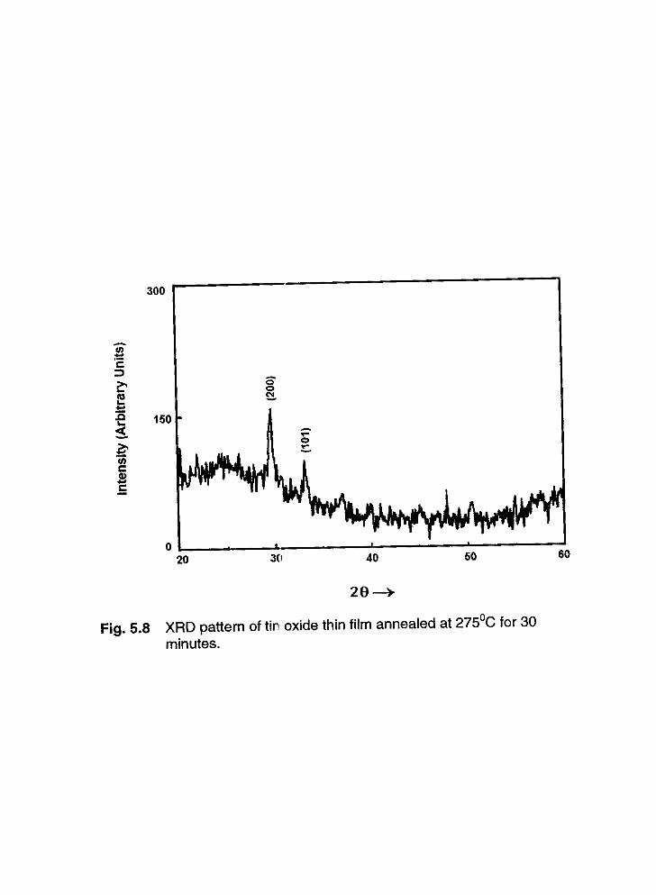
Fig. 5.8 XRD pattem of tin oxide thin film annealed at 275'~ for 30 minutes.
of x, which takes the crystalline structure of Sn02 more easily, on
annealing, than does a film dept~sited at a high substrate temperature.
The composition of the reactively evaporated films are between
stoichiometric SnOx and SnO:, where x ranges from 1.25 to 1.57 and
corresponds to intermediate oxide Sn304 with x = 1 .33.2' The structure of
amorphous SnO films can be assumed to consist of slightly distorted,
corner connected oxygen octahedral having central sn4' ions and strained
octahedra. These strained octahedra possess sn2' ions and oxygen
vacancies. The presence of diqerent oxidation states is mainly influenced
by the production procedure and post-deposition annealing conditions.
5.4 Indium Tin Oxide
Indium tin oxide thin films have been prepared by reactively
evaporating different alloys of indium and tin (Indium: Tin = 80: 20, 85: 15,
90: 10 and 95: 5 by weight percentage) from a tantalum boat in a vacuum
coating unit. The method of making alloy is described in chapter 3 section
3.5.The deposition conditions are also described in section 3.5 .The films
are prepared at a substrate temperature of 2 0 0 ' ~ in an oxygen
atmosphere with various tin concentrations. The thickness of the films are
500 nm each. X ray spectra are recorded using the X ray diffractometer
(Philips- PW3710). The radiation used is Cu Ka and the operating
potential is 25 kV at 10 mA.
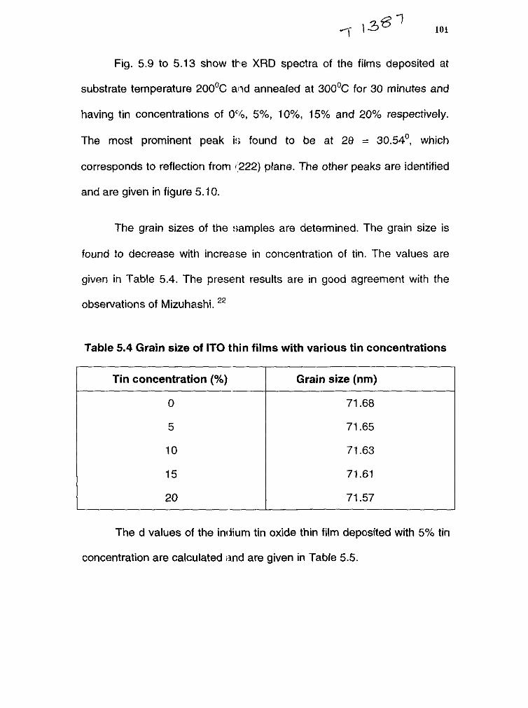
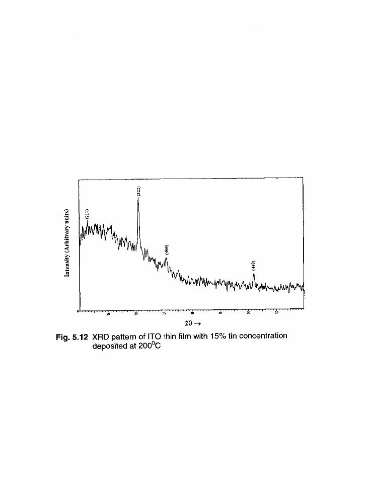
Fig. 5.9 to 5.13 show the XRD spectra of the films deposited at
substrate temperature 200% alid annealed at 3 0 0 ' ~ for 30 minutes and
having tin concentrations of O'/O, 574, lo%, 15% and 20% respectively.
The most prominent peak i!; found to be at 28 = 30.54', which
corresponds to reflection from 1222) plane. The other peaks are identified
and are given in figure 5.10.
The grain sizes of the samples are determined. The grain size is
found to decrease with increase in concentration of tin. The values are
given in Table 5.4. The present results are in good agreement with the
observations of Mizuhashi. 22
Table 5.4 Grain size of IT0 thin films with various tin concentrations
Tin concentration (%) I Grain size (nm)
The d values of the indium tin oxide thin film deposited with 5% tin
concentration are calculated and are given in Table 5.5.

Fig. 5.9 XRD pattern of indium oxide thin film deposited at 200'~
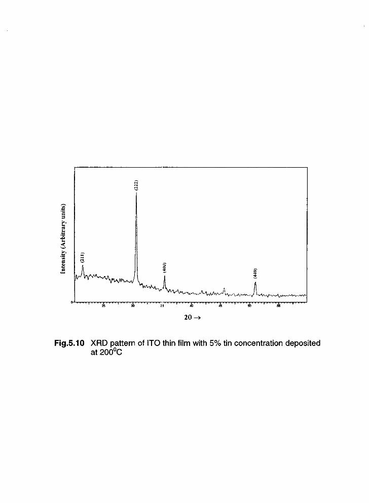
Fig.5.10 XRD pattern of IT0 thin film with 5% tin concentration deposited at 200°C

Fig.5.11 XRD pattern of 11.0 thin film with 10% tin concentration deposited at 200°C
--. ,.. a . . a . . . . , . . . . . _ I 0 U B
20 + Fig. 5.12 XRD pattern of IT0 rhin film with 15% tin concentration
deposited at 200%

5.13 XRD pattern of IT0 thin film with 20% tin concentration deposited at 200°C

Table 5.5 The calculated d values for Ts = 2 0 0 ' ~ along with the standard d values from ASTM data for IT0 thin film with 5% tin concentration
Calculated
1.789
ASTM
It is found that the c;ilculated values agree well with the ASTM
data. The film exhibits the reflection from the (222) planes as the most
predominant peak in the X- ray diffraction pattern. None of the spectra
indicated any characteristic peaks of Sn, SnO or Sn02, which indicates
that the tin atoms are doped substitutionally into the indium oxide lattice.
For all the three materials, the peaks obtained in the diffraction
spectra are sharp indicating (he highly crystalline nature of the films.
Studies on the grain size on indium oxide thin films show that the
grain size increases with increase in substrate temperature. Grain size of
tin oxide thin films increases with increase in annealing temperature.
Grain size of IT0 thin films is found to decrease with increase in tin
concentration.
References
1. K. K. Makhija, A. Ray, R. M. Patel, U. B. Trivedi, H. N. Kapse, Bull.
Mat. Sci., 28 (2005) 9.
2. M. H. M. Reddy and I\. N. Chandorkar, Sensors and Actuators 6,
9 (1 992) 1.
3. G. Sberveglieri, P. Bcinussi, S. Groppelli and P. Nelli, Thin Solid
Films, 186 (1 990) 349
4. Landolt, Bornstein, Numerical Data and Functional Relationships in
Science and Technology, New Series (Springer, Verlag 11 117 bl.
64, 1975).
5. J. Robertson, J. Phys. C. Solid State Phys., 12 (1 979) 4767
6. J. C. C. Fan and F. J. Eachner, J. Electrochem. Soc., 122 (1975) 1719.
7. J. L. Vossen, RCA Rev., 32 (1 971) 289.
8. H. W. Lehrnann and FI. Widrner, Thin Solid Films, 27 (1975) 359.
9. 0. P. Agnihotri, A. kc. Sharrna, 8. K. Gupta and R. Thankaraj,
J. Phys. D. Appl. Phys., 11 (1978) 643.
10. K. F. Huang, T. M. Uen, Y. S. Gou, C.R. Huang and H. C. Yang,
Thin Solid Films, 148 (1 987) 7.
11. P. Thilakan and J. Kumar, Vacuum, 48(1997) 463.
12. F. Iwatsu, T. Kobayashi and N. Uyea, J. Phys. Chem.,
83 (1 980) 3223.
13. A. Goswami and A. P. Goswami, Pramana, 8 (1977) 335.
14. R. P. Burns, J. Chem. Phys., 44 (1 966) 3307.
15. K. 8. Sundaram and G. K. Bhagavat, Phy. Stat. Sol., 63 (1981)
K15.
16. S. Weng, H. Wynands and M. Cocivera, Chem. Mater.,
4 (1992) 1428.
17. S. Mirzapour, S. M. Rozati, M. G. Takwale, B. R. Marathe,
V. G. Bhide, Mater. Res. Bull., 27 (1 992) 1 133.
18. S. Naseem, I. A. Rauf, K. Hussain, N. A. Malik, Thin Solid Films,
126 (1 988) 161.
19. M. H. M. Reddy, S. R. Jawalekar and A. N. Chandorkar, Thin Solid
Films, 169 (1 989) 11 7.
20. T. Yamazaki, U. Mi2:utani and Y. Iwama, Jpn. J. Appl. Phys.,
21 (1 982) 440.
21. H. G. Newman, P. Zeggel and K. Melzer, J. Non-Cryst Solids, 108
(1 989) 128.
22. M. Mizuhashi, Thin Solid Films, 76 (1981) 97.