STRUCTURAL IMPERFECTIONS (DEFECTS) IN CRYSTALLINE...
23
STRUCTURAL IMPERFECTIONS (DEFECTS) IN CRYSTALLINE SOLIDS
Transcript of STRUCTURAL IMPERFECTIONS (DEFECTS) IN CRYSTALLINE...
STRUCTURAL IMPERFECTIONS
(DEFECTS)
IN CRYSTALLINE SOLIDS

Real Crystalline solids are almost never perfect. These imperfections can be classified according to their dimensionality:
1. Point defects (0-Dimension)
2. Line defects (1-D)
3. Interfacial defects (2-D)
4. Bulk defects (3-D)

Relative Size Ranges of Defects
10-6 10-8 102 101 100 10-2 10-4 10-12
Electronic point defect
Atomic point defect
Line defect Bulk defect
Interfacial defect
cm

1. POINT DEFECTS
These are defects of atomic dimensions that usually result from:
1. The presence of an impurity atom
Substitutional →larger atoms
Interstitial → smaller atoms
2. The absence of a matrix atom (vacancy)
3. The presence of a matrix atom in a wrong
place (self-interstitial)

• Vacancies: -vacant atomic sites in a structure.
• Self-Interstitials: -"extra" atoms positioned between atomic sites.
Point Defects
Vacancy
distortion
of planes
self- interstitial
distortion of planes

Presence of an impurity atom: -"extra" atoms positioned between atomic sites.
Substitutional
Interstitial

The point defects discussed so far occur in metallic structures. Those in ionic structures differ because of the charge neutrally requirement.
An anion
and a cation
is missing
An anion or a
cation is at an
insterstital site

• are line defects,
• slip between crystal planes result when dislocations move,
• produce permanent (plastic) deformation.
Dislocations:
Schematic of Zinc (HCP):
• before deformation • after tensile elongation
slip steps
2. Line Defects (Dislocations)
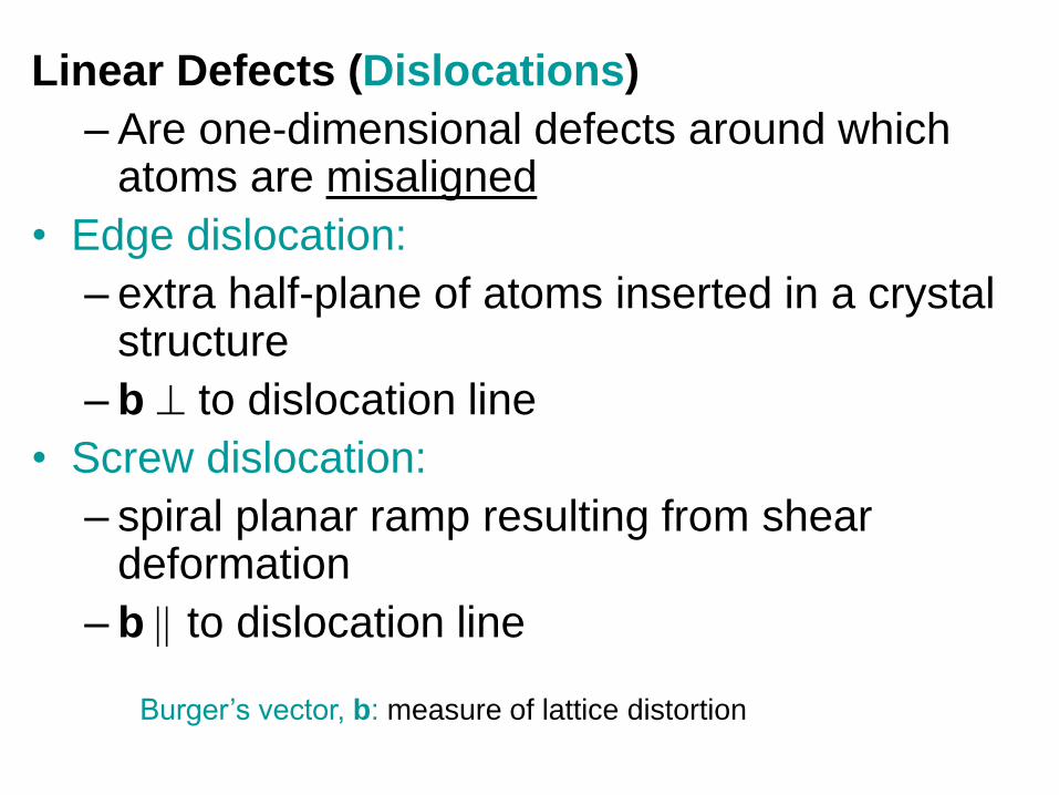
Linear Defects (Dislocations)
– Are one-dimensional defects around which atoms are misaligned
• Edge dislocation:
– extra half-plane of atoms inserted in a crystal structure
– b to dislocation line
• Screw dislocation:
– spiral planar ramp resulting from shear deformation
– b to dislocation line
Burger’s vector, b: measure of lattice distortion

First a closed circuit is drawn around the dislocation by jumping from one atom to another.
The same number of jumps will be made in a perfect system.
The vector needed to complete the circuit is called BURGER VECTOR.

Edge Dislocations
Burger’s vector is perpendicular to dislocation in edge dislocations.
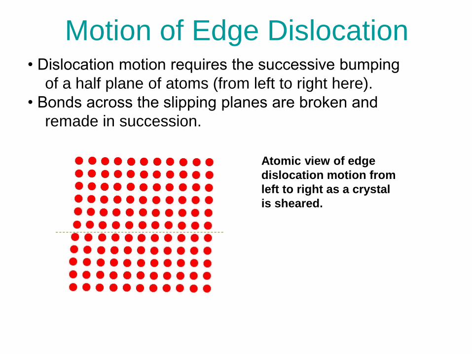
• Dislocation motion requires the successive bumping
of a half plane of atoms (from left to right here).
• Bonds across the slipping planes are broken and
remade in succession.
Atomic view of edge
dislocation motion from
left to right as a crystal
is sheared.
Motion of Edge Dislocation

Screw Dislocations
Burger’s vector is parallel to dislocation in screw dislocations.


• Dislocations are simply slide or slip of one portion of crystal system over another as dislocations move one part of the system relative to the other.
• When dislocations pass through the whole system, the system permanently deforms.
• Dislocations are on boundary between the regions where slip has occured and where it has not.
• On either side of the dislocation crystalline system is essentially perfect.
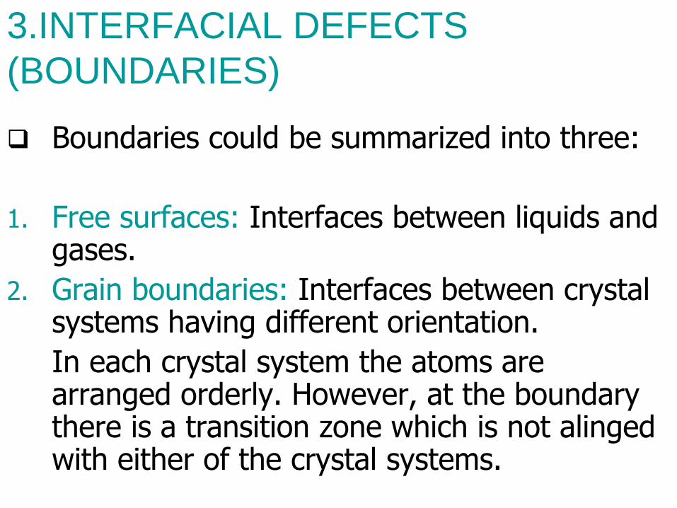
3.INTERFACIAL DEFECTS
(BOUNDARIES)
Boundaries could be summarized into three:
1. Free surfaces: Interfaces between liquids and gases.
2. Grain boundaries: Interfaces between crystal systems having different orientation.
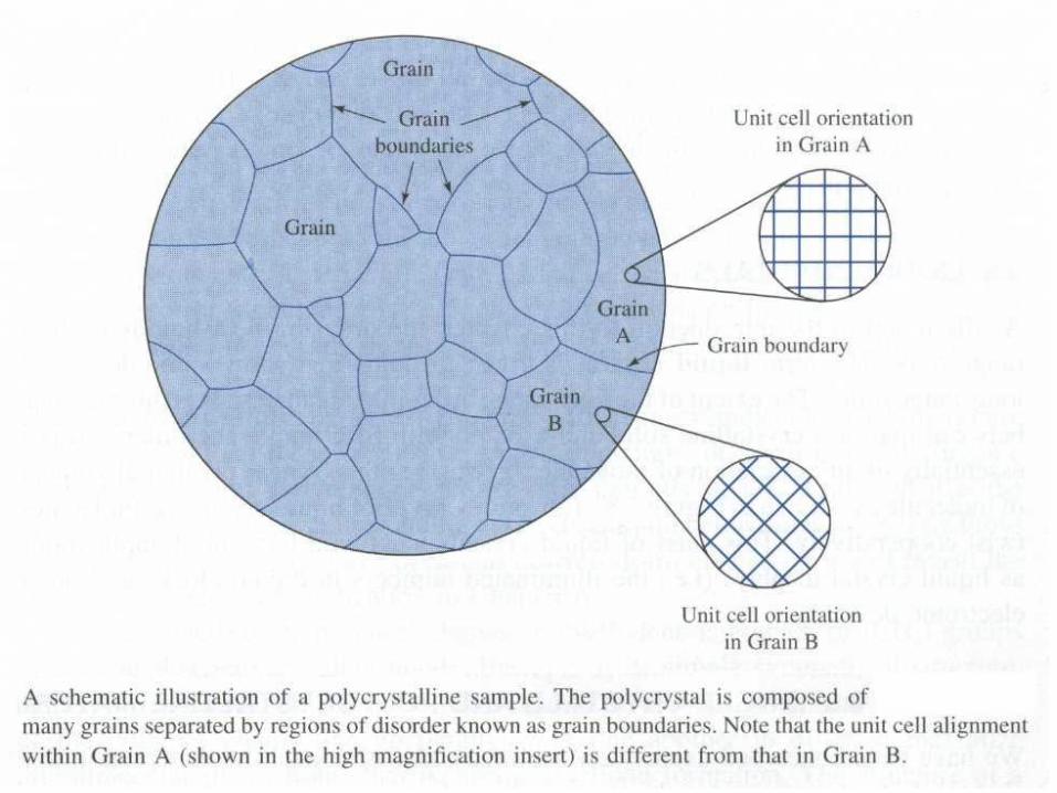
In each crystal system the atoms are arranged orderly. However, at the boundary there is a transition zone which is not alinged with either of the crystal systems.

3. Interphase boundaries: similar to grain
boundaries both in shape and behavior.
However, in these systems there are two or
more materials having different crystal
structures. Multiphase materials having a
change in physical and/or chemical
characteristics will also have interphase
boundaries. (Ex: ice-water)
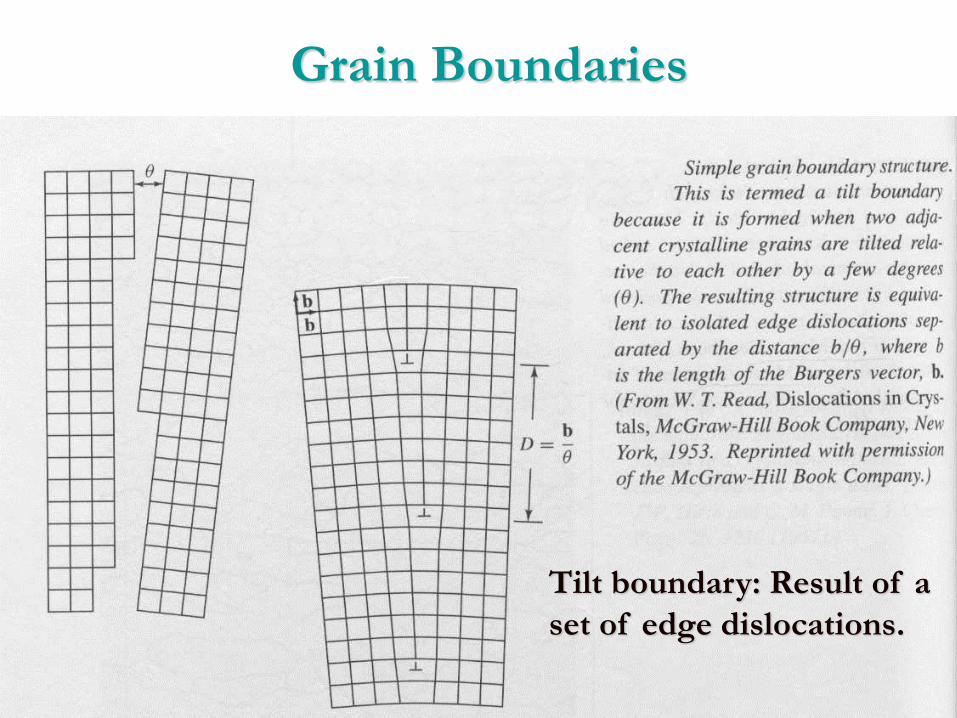
Grain Boundaries
Tilt boundary: Result of a
set of edge dislocations.

Twist boundary: Result of a set of screw
dislocations
Grain Boundaries

4. BULK DEFECTS
They are either introduced during the production of the material or during its fabrication.
For example → inclusions (cracks,
notches, air bubbles & etc.) added during
production.

IMPORTANCE OF IMPERFECTIONS
Most of the properties of materials are affected by imperfections:
Small amount of impurity atoms may increase the electrical conductivity of semi-conductors.
Dislocations are responsible for ductility. Strength of materials can be increased to a large extent by the mechanism “strain-hardening” which produces line defects that act as a barrier to control the growth of other imperfections.
Presence of bulk defects such as cracks, notches, holes causes brittle materials, which break at very low stresses without showing large deformations.


![Crystal Imperfections in Solids [7] - Unesp · Crystal Imperfections in Solids 3> ¾The atomic arrangements in a crystalline lattice is almost always not perfect. ¾There are “defects”](https://static.fdocuments.net/doc/165x107/5eb9eed0c37e1e5d6524b706/crystal-imperfections-in-solids-7-unesp-crystal-imperfections-in-solids-3.jpg)