STM-TunnelingSTM-Tunneling. STM-TunnelingSTM-Tunneling.
18
TelA viv U niversity STM-Tunneling STM-Tunneling
-
date post
21-Dec-2015 -
Category
Documents
-
view
326 -
download
1
Transcript of STM-TunnelingSTM-Tunneling. STM-TunnelingSTM-Tunneling.
Tel Aviv University
STM-TunnelingSTM-Tunneling
Tel Aviv University
STM-TunnelingSTM-Tunneling
Tel Aviv University
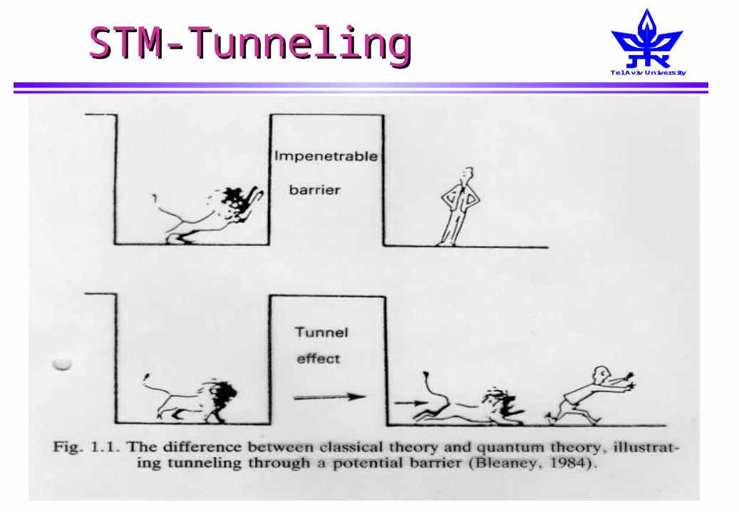
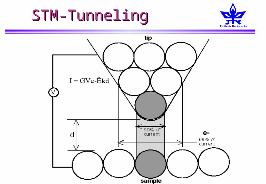
Why STM ? The electronic microscopes gives ‘volume images’ (penetration depth) In STM-no use of external particles Principle-Electrons tunneling between an atomically sharp tip and a surface
(animation-program files/netscape/communicator/program/stmanimation)
STM-IntroductionSTM-Introduction
Tel Aviv University
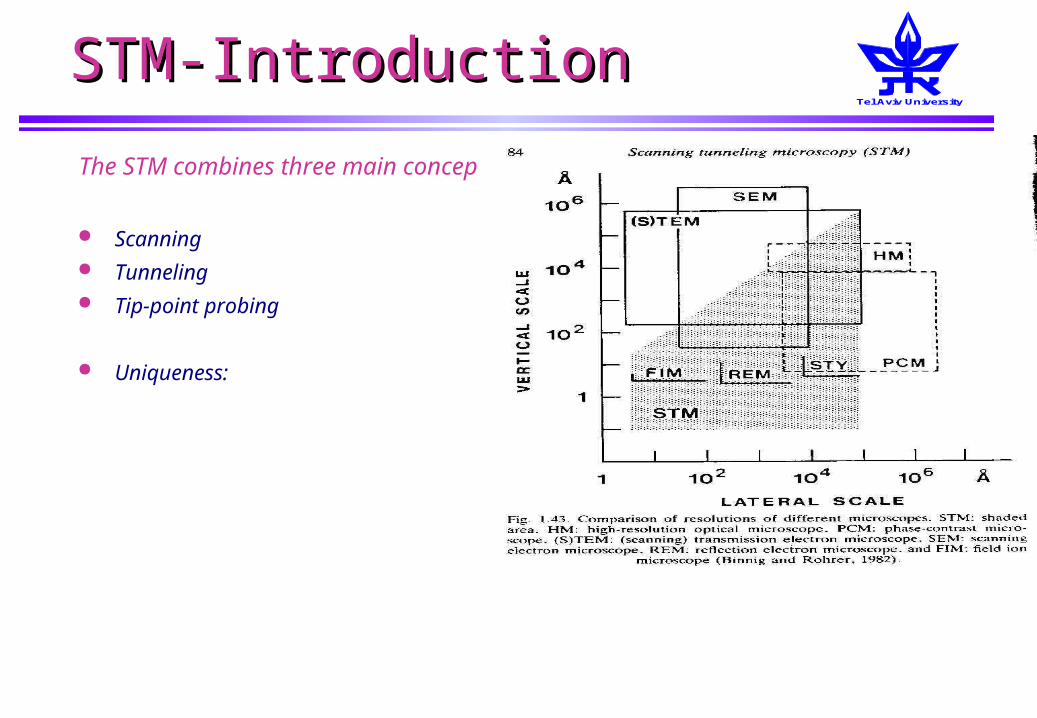
The STM combines three main concepts:
Scanning Tunneling Tip-point probing
Uniqueness:
STM-IntroductionSTM-Introduction
Tel Aviv University
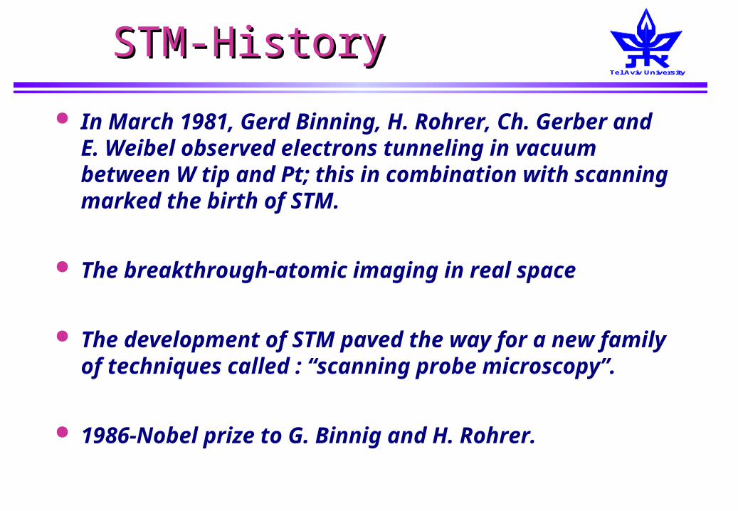
In March 1981, Gerd Binning, H. Rohrer, Ch. Gerber and E. Weibel observed electrons tunneling in vacuum between W tip and Pt; this in combination with scanning marked the birth of STM.
The breakthrough-atomic imaging in real space
The development of STM paved the way for a new family of techniques called : “scanning probe microscopy”.
1986-Nobel prize to G. Binnig and H. Rohrer.
STM-HistorySTM-History
Tel Aviv University
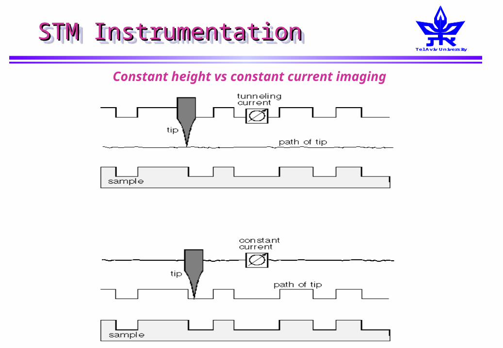
Constant height vs constant current imaging
STM InstrumentationSTM InstrumentationSTM InstrumentationSTM Instrumentation
Tel Aviv University
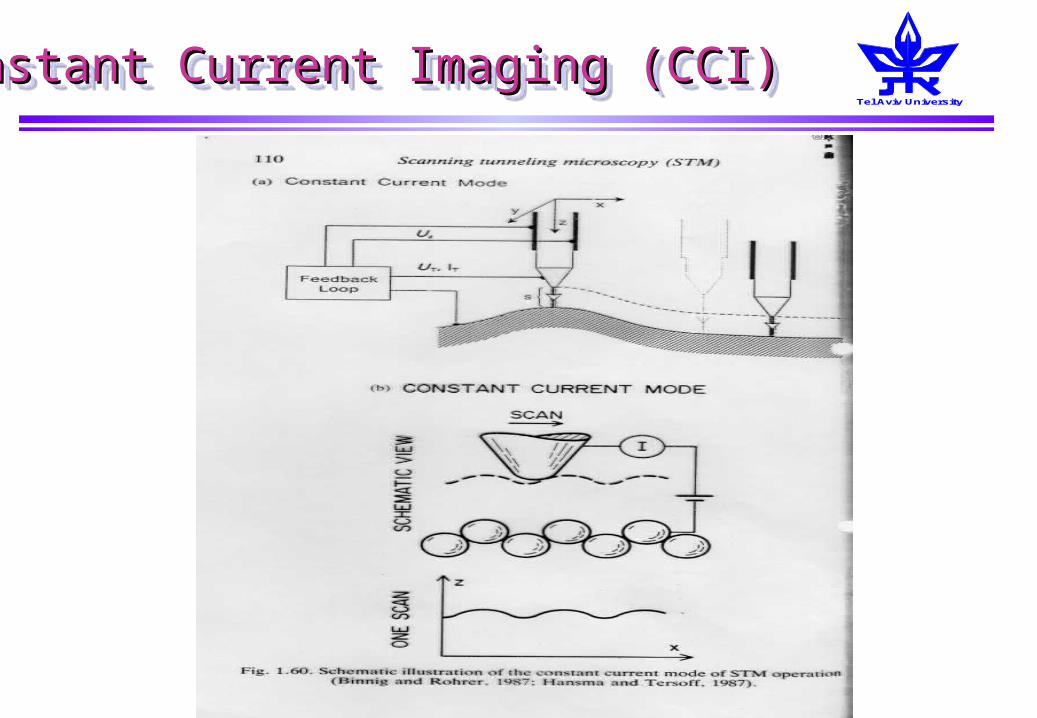
Constant Current Imaging (CCI)Constant Current Imaging (CCI)Constant Current Imaging (CCI)Constant Current Imaging (CCI)
Tel Aviv UniversityTel Aviv University
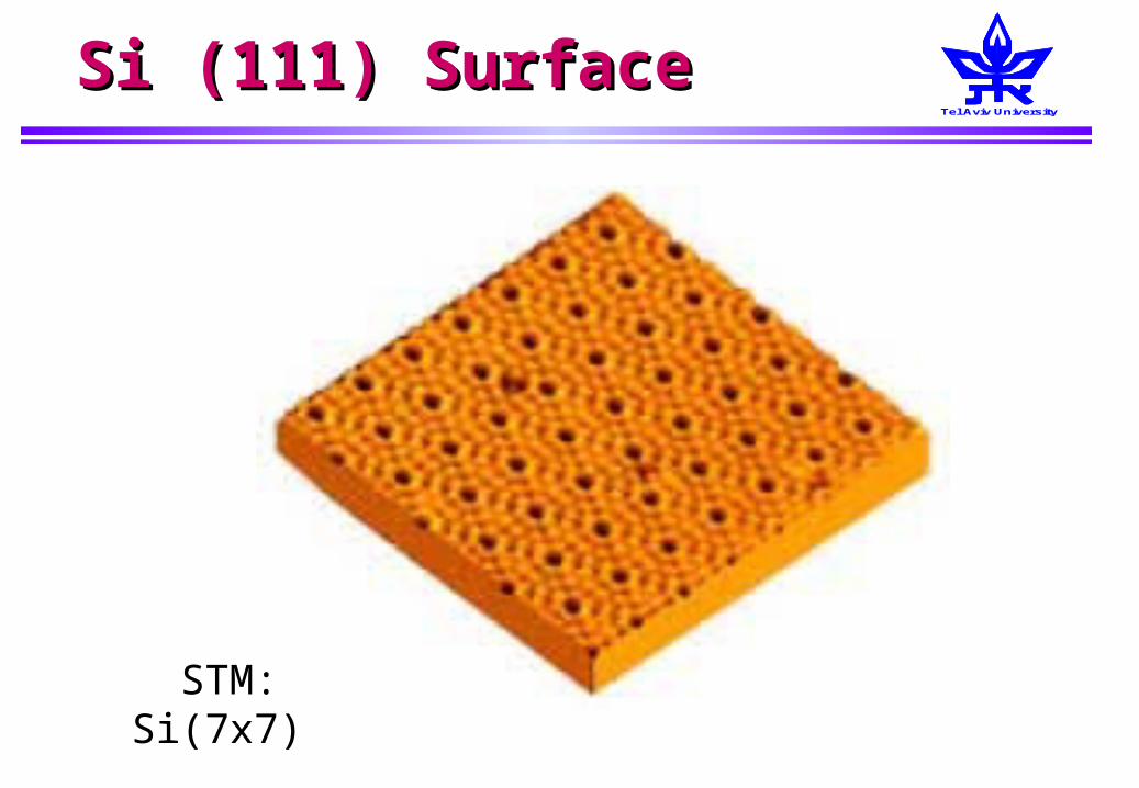
Si (111) SurfaceSi (111) Surface
STM: Si(7x7)
Tel Aviv University
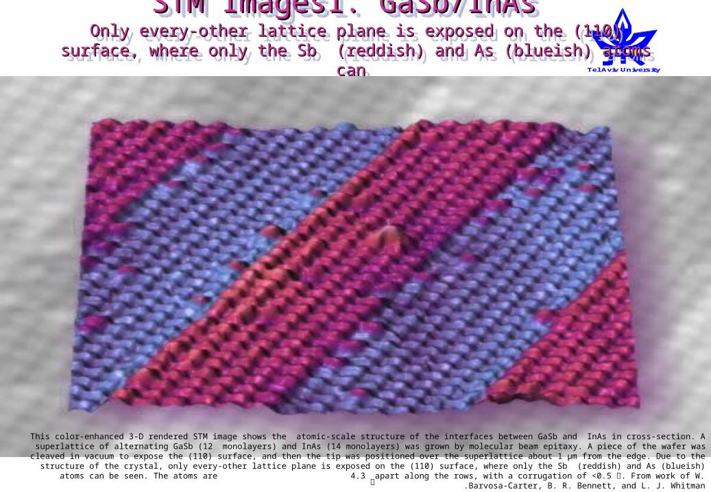
STM Images1. GaSb/InAsSTM Images1. GaSb/InAs Only every-other lattice plane is exposed on the (110) surface, where only the Sb Only every-other lattice plane is exposed on the (110) surface, where only the Sb
(reddish) and As (blueish) atoms can (reddish) and As (blueish) atoms can
STM Images1. GaSb/InAsSTM Images1. GaSb/InAs Only every-other lattice plane is exposed on the (110) surface, where only the Sb Only every-other lattice plane is exposed on the (110) surface, where only the Sb
(reddish) and As (blueish) atoms can (reddish) and As (blueish) atoms can
This color-enhanced 3-D rendered STM image shows the atomic-scale structure of the interfaces between GaSb and InAs in cross-section. A superlattice of alternating GaSb (12 monolayers) and InAs (14 monolayers) was grown by molecular beam epitaxy. A piece of the wafer was cleaved in vacuum to expose the (110) surface, and then the tip was positioned over the superlattice about 1 µm from the edge.
Due to the structure of the crystal, only every-other lattice plane is exposed on the (110) surface, where only the Sb (reddish) and As (blueish) atoms can be seen. The atoms are 4.3 ֵ apart along the rows, with a corrugation of <0.5 ֵ. From work of W. Barvosa-Carter, B. R. Bennett, and L. J. Whitman.
Tel Aviv University
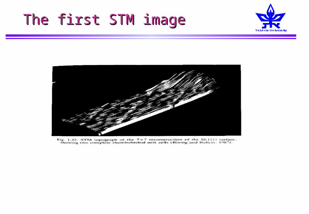
The first STM imageThe first STM image
Tel Aviv UniversityTel Aviv University
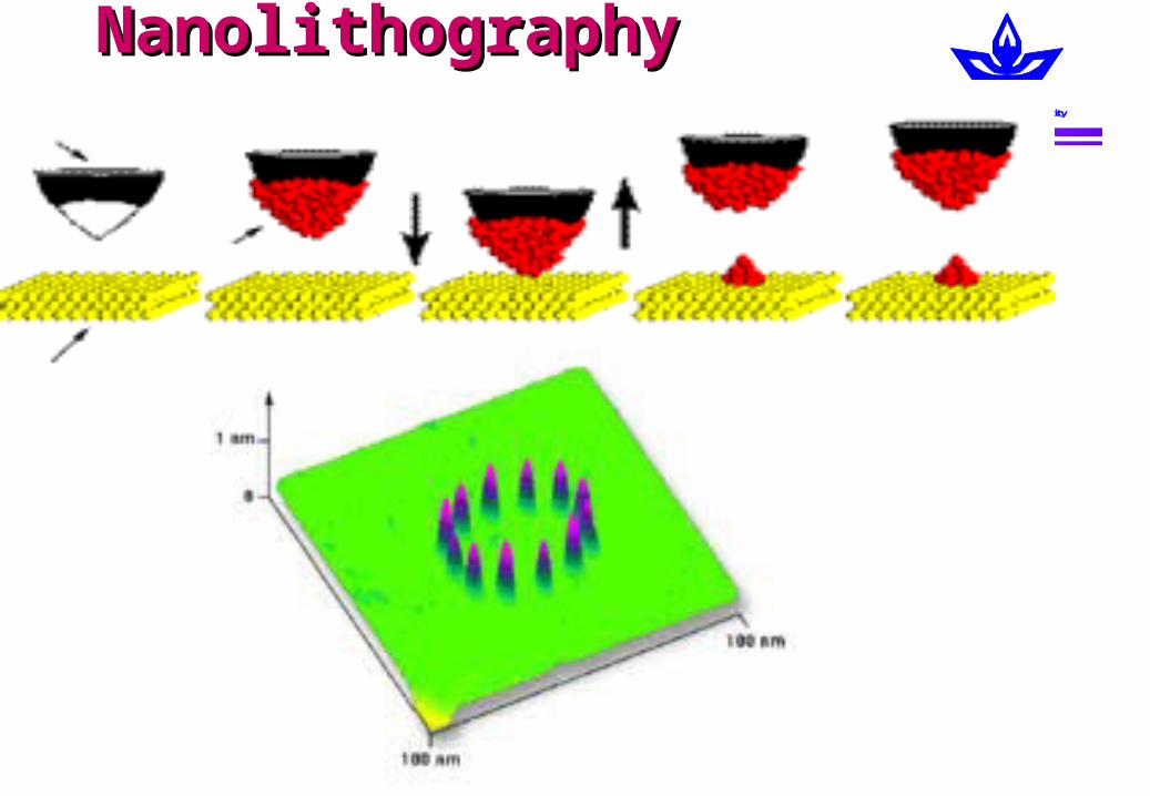
NanolithographyNanolithography
Tel Aviv University
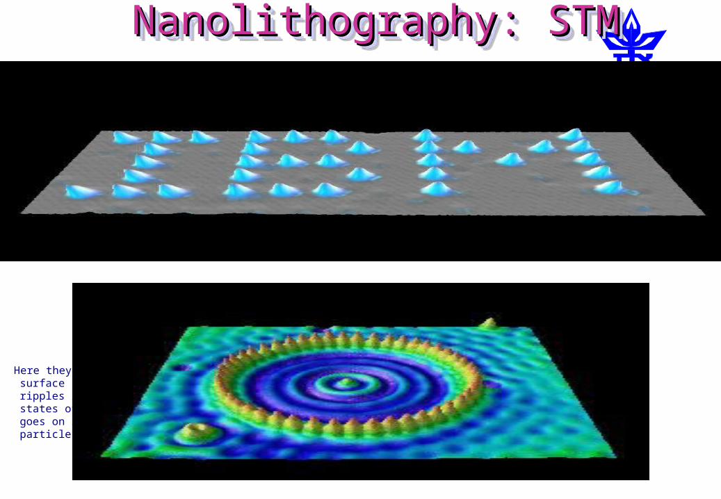
Nanolithography: STMNanolithography: STMNanolithography: STMNanolithography: STM
Here, the artist, shortly after discovering how to move atoms with the STM,
found a way to give something back to the corporation which gave him a job when he needed one and provided him with the tools he needed in order to be successful. (Xe on Nickel, Nature 344, 524 (1990).
Here they have positioned 48 iron atoms into a circular ring in order to "corral" some surface state electrons and force them into "quantum" states of the circular structure. The ripples in the ring of atoms are the density distribution of a particular set of quantum states of the corral. The artists were delighted to discover that they could predict what goes on in the corral by solving the classic eigenvalue problem in quantum mechanics -- a particle in a hard-wall box. [Crommie, Lutz & Eigler, Science 262, 218 (1993)]
Tel Aviv University
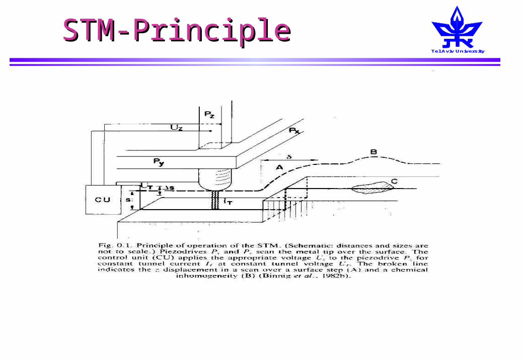
STM-PrincipleSTM-Principle
Tel Aviv University
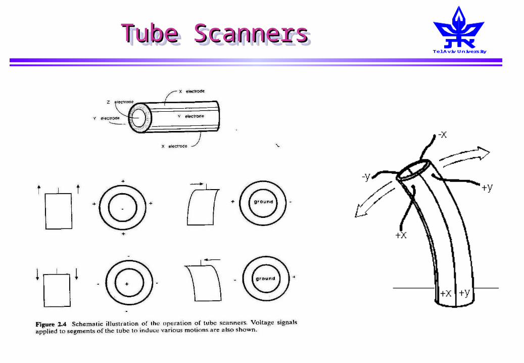
Tube ScannersTube ScannersTube ScannersTube Scanners
Tel Aviv University
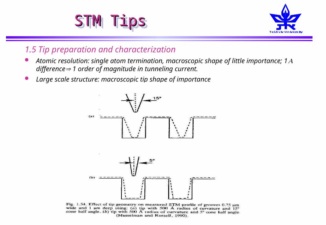
1.5 Tip preparation and characterization Atomic resolution: single atom termination, macroscopic shape of little importance; 1
difference 1 order of magnitude in tunneling current. Large scale structure: macroscopic tip shape of importance
STM TipsSTM TipsSTM TipsSTM Tips
Tel Aviv University
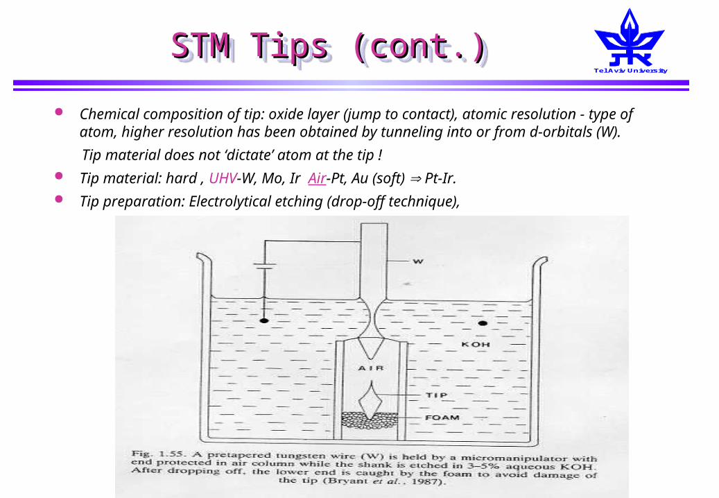
Chemical composition of tip: oxide layer (jump to contact), atomic resolution - type of atom, higher resolution has been obtained by tunneling into or from d-orbitals (W).
Tip material does not ‘dictate’ atom at the tip ! Tip material: hard , UHV-W, Mo, Ir Air-Pt, Au (soft) Pt-Ir. Tip preparation: Electrolytical etching (drop-off technique),
STM Tips (cont.)STM Tips (cont.)STM Tips (cont.)STM Tips (cont.)
Tel Aviv University
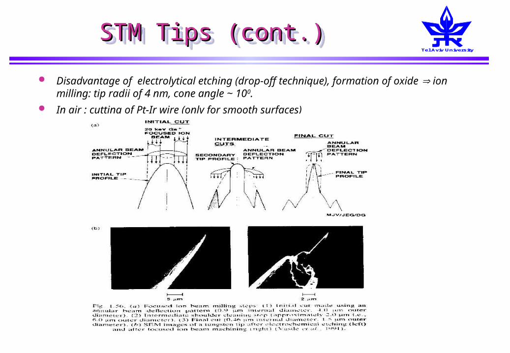
Disadvantage of electrolytical etching (drop-off technique), formation of oxide ion milling: tip radii of 4 nm, cone angle ~ 100.
In air : cutting of Pt-Ir wire (only for smooth surfaces)
STM Tips (cont.)STM Tips (cont.)STM Tips (cont.)STM Tips (cont.)
Tel Aviv University
STM Tips (cont.)STM Tips (cont.)STM Tips (cont.)STM Tips (cont.)
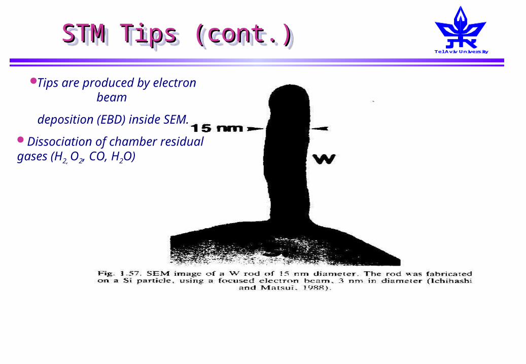
Tips are produced by electron beam
deposition (EBD) inside SEM.
Dissociation of chamber residual gases (H2, O2, CO, H2O)