Stereo PDM-to-I TDM Conversion IC Data Sheet · PDF file · 2016-11-08TDM...
17
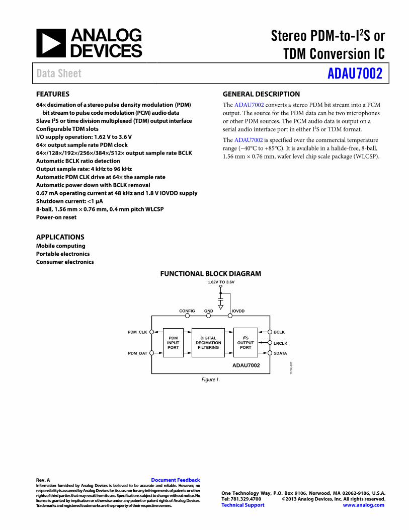
Stereo PDM-to-I 2 S or TDM Conversion IC Data Sheet ADAU7002 Rev. A Document Feedback Information furnished by Analog Devices is believed to be accurate and reliable. However, no responsibility is assumed by Analog Devices for its use, nor for any infringements of patents or other rights of third parties that may result from its use. Specifications subject to change without notice. No license is granted by implication or otherwise under any patent or patent rights of Analog Devices. Trademarks and registered trademarks are the property of their respective owners. One Technology Way, P.O. Box 9106, Norwood, MA 02062-9106, U.S.A. Tel: 781.329.4700 ©2013 Analog Devices, Inc. All rights reserved. Technical Support www.analog.com FEATURES 64× decimation of a stereo pulse density modulation (PDM) bit stream to pulse code modulation (PCM) audio data Slave I 2 S or time division multiplexed (TDM) output interface Configurable TDM slots I/O supply operation: 1.62 V to 3.6 V 64× output sample rate PDM clock 64×/128×/192×/256×/384×/512× output sample rate BCLK Automatic BCLK ratio detection Output sample rate: 4 kHz to 96 kHz Automatic PDM CLK drive at 64× the sample rate Automatic power down with BCLK removal 0.67 mA operating current at 48 kHz and 1.8 V IOVDD supply Shutdown current: <1 µA 8-ball, 1.56 mm × 0.76 mm, 0.4 mm pitch WLCSP Power-on reset APPLICATIONS Mobile computing Portable electronics Consumer electronics GENERAL DESCRIPTION The ADAU7002 converts a stereo PDM bit stream into a PCM output. The source for the PDM data can be two microphones or other PDM sources. The PCM audio data is output on a serial audio interface port in either I 2 S or TDM format. The ADAU7002 is specified over the commercial temperature range (−40°C to +85°C). It is available in a halide-free, 8-ball, 1.56 mm × 0.76 mm, wafer level chip scale package (WLCSP). FUNCTIONAL BLOCK DIAGRAM Figure 1. PDM_CLK CONFIG GND 1.62V TO 3.6V IOVDD PDM_DAT BCLK LRCLK SDATA PDM INPUT PORT DIGITAL DECIMATION FILTERING ADAU7002 11265-001 I 2 S OUTPUT PORT
Transcript of Stereo PDM-to-I TDM Conversion IC Data Sheet · PDF file · 2016-11-08TDM...
Stereo PDM-to-I2S or TDM Conversion IC
Data Sheet ADAU7002
Rev. A Document Feedback Information furnished by Analog Devices is believed to be accurate and reliable. However, no responsibility is assumed by Analog Devices for its use, nor for any infringements of patents or other rights of third parties that may result from its use. Specifications subject to change without notice. No license is granted by implication or otherwise under any patent or patent rights of Analog Devices. Trademarks and registered trademarks are the property of their respective owners.
One Technology Way, P.O. Box 9106, Norwood, MA 02062-9106, U.S.A. Tel: 781.329.4700 ©2013 Analog Devices, Inc. All rights reserved. Technical Support www.analog.com
FEATURES 64× decimation of a stereo pulse density modulation (PDM)
bit stream to pulse code modulation (PCM) audio data Slave I2S or time division multiplexed (TDM) output interface Configurable TDM slots I/O supply operation: 1.62 V to 3.6 V 64× output sample rate PDM clock 64×/128×/192×/256×/384×/512× output sample rate BCLK Automatic BCLK ratio detection Output sample rate: 4 kHz to 96 kHz Automatic PDM CLK drive at 64× the sample rate Automatic power down with BCLK removal 0.67 mA operating current at 48 kHz and 1.8 V IOVDD supply Shutdown current: <1 µA 8-ball, 1.56 mm × 0.76 mm, 0.4 mm pitch WLCSP Power-on reset
APPLICATIONS Mobile computing Portable electronics Consumer electronics
GENERAL DESCRIPTION The ADAU7002 converts a stereo PDM bit stream into a PCM output. The source for the PDM data can be two microphones or other PDM sources. The PCM audio data is output on a serial audio interface port in either I2S or TDM format.
The ADAU7002 is specified over the commercial temperature range (−40°C to +85°C). It is available in a halide-free, 8-ball, 1.56 mm × 0.76 mm, wafer level chip scale package (WLCSP).
FUNCTIONAL BLOCK DIAGRAM
Figure 1.
PDM_CLK
CONFIG GND
1.62V TO 3.6V
IOVDD
PDM_DAT
BCLK
LRCLK
SDATA
PDMINPUTPORT
DIGITALDECIMATIONFILTERING
ADAU7002
1126
5-00
1
I2SOUTPUT
PORT

ADAU7002* Product Page Quick LinksLast Content Update: 08/30/2016
Comparable PartsView a parametric search of comparable parts
Evaluation Kits• ADAU7002Z Evaluation Board
DocumentationData Sheet• ADAU7002: Stereo PDM-to-I2S or TDM Conversion IC
Data SheetUser Guides• UG-533: Evaluating the ADAU7002 Using the EVAL-
ADAU7002Z
Tools and Simulations• ADAU7002 IBIS Model
Design Resources• ADAU7002 Material Declaration• PCN-PDN Information• Quality And Reliability• Symbols and Footprints
DiscussionsView all ADAU7002 EngineerZone Discussions
Sample and BuyVisit the product page to see pricing options
Technical SupportSubmit a technical question or find your regional support number
* This page was dynamically generated by Analog Devices, Inc. and inserted into this data sheet. Note: Dynamic changes to the content on this page does not constitute a change to the revision number of the product data sheet. This content may be frequently modified.

ADAU7002 Data Sheet
Rev. A | Page 2 of 16
TABLE OF CONTENTS Features .............................................................................................. 1 Applications ....................................................................................... 1 General Description ......................................................................... 1 Functional Block Diagram .............................................................. 1 Revision History ............................................................................... 2 Specifications ..................................................................................... 3 Absolute Maximum Ratings ............................................................ 4
Thermal Resistance ...................................................................... 4 ESD Caution .................................................................................. 4
Pin Configuration and Function Descriptions ..............................5 Typical Performance Characteristics ..............................................6 Typical Application Circuit ..............................................................8 Applications Information .................................................................9
Overview ........................................................................................9 Clocking..........................................................................................9 Serial Audio Output Interface .....................................................9
Outline Dimensions ....................................................................... 13 Ordering Guide .......................................................................... 13
REVISION HISTORY 7/13—Rev. 0 to Rev. A
Changes to Supply Current Test Conditions/Comments ............ 3 Changes to Figure 5 .......................................................................... 6 Added Figure 6; Renumbered Sequentially .................................. 6 Changes to Figure 14 and Figure 15............................................. 10 Changes to Figure 16, Figure 17, and Figure 18 ......................... 11 Changes to Figure 19, Figure 20, and Figure 21 ......................... 12
1/13—Revision 0: Initial Version

Data Sheet ADAU7002
Rev. A | Page 3 of 16
SPECIFICATIONS IOVDD = 1.8 V, TA = 25°C, BCLK = 3.072 MHz, output = 48 kHz, I2S format, unless otherwise noted.
Table 1. Parameter Test Conditions/Comments Min Typ Max Unit DIGITAL INPUT/OUTPUT
High Level Input Voltage (VIH) 0.7 × IOVDD V Low Level Input Voltage (VIL) 0.3 × IOVDD V Input Leakage, High (IIH) BCLK and LRCLK pins 1 µA Input Leakage, Low (IIL) BCLK and LRCLK pins 1 µA Input Capacitance 5 pF
SDATA 4.5 mA PDM_CLK 9 mA
PERFORMANCE Dynamic Range 20 Hz to 20 kHz, −60 dB input
With A-Weighted Filter (RMS) 110 dB Signal-to-Noise-Ratio A-weighted, fourth-order input 110 dB Decimation Ratio 64× Frequency Response DC to 0.45 output fS −0.1 +0.01 dB Stop Band 0.566 fS Stop-Band Attenuation 60 dB Group Delay 0.02 fS input signal 3.31 LRCLK cycles Gain PDM to PCM 0 dB Start-Up Time 48 LRCLK cycles Bit Width Internal and output 20 Bits Interchannel Phase 0 Degrees
CLOCKING Output Sampling Rate fS LRCLK pulse rate 4 48 96 kHz BCLK Frequency fBCLK 0.256 3.072 24.576 MHz
POWER SUPPLIES Supply Voltage Range IOVDD 1.62 3.6 V Supply Current IOVDD = 1.8 V 0.67 mA IOVDD = 3.3 V 1.33 mA IOVDD = 1.8 V, 16 kHz output 0.21 mA IOVDD = 3.3 V, 16 kHz output 0.41 mA Shutdown Current IOVDDSD, no input clocks 1 µA

ADAU7002 Data Sheet
Rev. A | Page 4 of 16
ABSOLUTE MAXIMUM RATINGS Absolute maximum ratings apply at 25°C, unless otherwise noted.
Table 2. Parameter Rating IOVDD Supply Voltage 3.6 V Input Voltage 3.6 V
ESD Susceptibility 4 kV Storage Temperature Range −65°C to +150°C Operating Temperature Range −40°C to +85°C Junction Temperature Range −65°C to +165°C Lead Temperature (Soldering, 60 sec) 300°C
Stresses above those listed under Absolute Maximum Ratings may cause permanent damage to the device. This is a stress rating only; functional operation of the device at these or any other conditions above those indicated in the operational section of this specification is not implied. Exposure to absolute maximum rating conditions for extended periods may affect device reliability.
THERMAL RESISTANCE θJA (junction to air) is specified for the worst-case conditions, that is, a device soldered in a circuit board for surface-mount packages. θJA is determined according to JESD51-9 on a 4-layer printed circuit board (PCB) with natural convection cooling.
Table 3. Thermal Resistance Package Type θJA Unit 8-ball, 1.56 mm × 0.76 mm WLCSP 90 °C/W
ESD CAUTION

Data Sheet ADAU7002
Rev. A | Page 5 of 16
PIN CONFIGURATION AND FUNCTION DESCRIPTIONS
Figure 2. Pin Configuration (Top Side View)
Table 4. Pin Function Descriptions Pin No. Mnemonic Type Description A1 PDM_DAT Input PDM Data Input A2 PDM_CLK Output PDM Clock Output B1 SDATA Output Serial Data Output for I2S/TDM B2 BCLK Input Bit Clock for I2S/TDM C1 GND Ground Ground C2 LRCLK Input Left/Right Clock for I2S/Frame Sync for TDM D1 IOVDD Supply Input/Output and Digital Supply D2 CONFIG Input Configuration Pin
TOP VIEW(BALL SIDE DOWN)
1126
5-00
2
BALL A1CORNER
A PDM_DAT
PDM_CLK
SDATA BCLK
GND LRCLK
IOVDD CONFIG
21
B
C
D

ADAU7002 Data Sheet
Rev. A | Page 6 of 16
TYPICAL PERFORMANCE CHARACTERISTICS
Figure 3. FFT, fS = 48 kHz, −60 dBFS Input
Figure 4. Frequency Response
Figure 5. Group Delay vs. Normalized Frequency (Relative to fS)
Figure 6. Group Delay vs. Frequency, fS = 48 kHz
Figure 7. Total Harmonic Distortion + Noise (THD + N) vs.
Normalized Frequency (Relative to fS)
Figure 8. THD + N Level vs. Generator Level
0–10–20–30–40–50–60–70–80–90
–100–110–120–130–140–150–160–170–180–190
LEVE
L (d
BFS
)
FREQUENCY (Hz)20 100 1k 10k 20k
CH1CH2
1126
5-00
3
–0.5
–0.4
–0.3
–0.2
–0.1
0
0.1
0.0001 0.001 0.01 0.1 1
LEVE
L (d
BFS
)
1126
5-00
4
NORMALIZED FREQUENCY (RELATIVE TO fS) (Hz)
0
1
2
3
4
6
5
7
8
GR
OU
P D
ELAY
(LR
CLK
CYC
LES)
1126
5-10
0
NORMALIZED FREQUENCY (RELATIVE TO fS) (Hz)0.0001 0.001 0.01 0.1 1
0
20
40
60
80
120
100
140
160
GR
OU
P D
ELAY
(µs)
1126
5-10
1
FREQUENCY (Hz)10 100 1k 10k 100k
0.0001 0.001 0.01 0.1 1–140
–120
–100
–80
–60
–20
–40
0
THD
+ N
(dB
FS)
1126
5-00
6
NORMALIZED FREQUENCY (RELATIVE TO fS) (Hz)
–120
–100
–80
–60
–40
–20
0
–120 –100 –80 –60 –40 –20 0
THD
+ N
LEV
EL (d
BFS
)
GENERATOR LEVEL (dBFS) 1126
5-00
7

Data Sheet ADAU7002
Rev. A | Page 7 of 16
Figure 9. Supply Current vs. Supply Voltage
Figure 10. Out-of-Band Frequency Response (48 kHz Output)
0.4
0.5
0.6
0.7
0.8
0.9
1.0
1.1
1.2
1.3
1.4
1.6 1.8 2.0 2.2 2.4 2.6 2.8 3.0 3.2 3.4
SUPP
LY C
UR
REN
T (m
A)
SUPPLY VOLTAGE (V) 1126
5-00
90
–20
–40
–60
–80
–100
–120
–140
–160
MA
GN
ITU
DE
(dB
)
FREQUENCY (MHz)0 0.5 1.0 1.5
1126
5-01
0

ADAU7002 Data Sheet
Rev. A | Page 8 of 16
TYPICAL APPLICATION CIRCUIT
Figure 11. Typical Application Circuit
PDM_CLK
CONFIG
GND
IOVDD
0.1µF
IOVDD
PDM_DAT
PDM_CLK
CONFIG
PDM_DAT
LRCLK
SDATA
BCLK
ADAU7002
LRCLK
SDATA
OPTIONALPULL-DOWNRESISTOR
BCLK
1126
5-01
1

Data Sheet ADAU7002
Rev. A | Page 9 of 16
APPLICATIONS INFORMATION OVERVIEW The ADAU7002 provides stereo decimation from a 1-bit PDM source to a 20-bit PCM audio. The downsampling ratio is fixed at 64×. The 20-bit downsampled PCM audio is output via standard I2S or TDM formats.
The input source for the ADAU7002 can be any device that has a PDM output, such as a digital microphone like the ADMP521. The output pins of these microphones can connect directly to the input pins of the ADAU7002.
CLOCKING The ADAU7002 requires a BCLK rate that is a minimum of 64× the LRCLK sample rate. BCLK rates of 128×, 192×, 256×, 384×, and 512× the LRCLK rate are also supported. The ADAU7002 automatically detects the ratio between BCLK and LRCLK and generates a PDM clock output at 64× the LRCLK rate. The minimum sample rate is 4 kHz, and the maximum is 96 kHz, which correspond to a PDM clock range of 256 kHz to 6.144 MHz. Internally, all processing is done at the PDM_CLK rate.
When BCLK is removed, the ADAU7002 powers down automatically. When BCLK is not present, the PDM_CLK output stops.
Table 5. PDM Timing Parameters Parameter tMIN tMAX Unit Data Setup Time, tSETUP 10 ns Data Hold Time, tHOLD 7 ns
PDM data is latched on both edges of the clock.
Figure 12. PDM Timing Diagram
SERIAL AUDIO OUTPUT INTERFACE The ADAU7002 supports I2S and TDM serial output formats. Format selection and TDM slot placement is set with the CONFIG pin. The SDATA pin is in tristate mode, except when the port is driving serial data based on the CONFIG pin configuration.
Table 6. TDM Slot Selection Device Setting CONFIG Pin Configuration I2S Format Tie to IOVDD TDM Slot 1 to Slot 2 Used/Driven, 32-Bit Slots Tie to GND TDM Slot 3 to Slot 4 Used/Driven, 32-Bit Slots Open
TDM Slot 5 to Slot 6 Used/Driven, 32-Bit Slots Tie to IOVDD through a 47 kΩ resistor
TDM Slot 7 to Slot 8 Used/Driven, 32-Bit Slots Tie to GND through a 47 kΩ resistor
RL
tHOLD
tSETUP
PDM_CLK
PDM_DAT R L
1126
5-01
2

ADAU7002 Data Sheet
Rev. A | Page 10 of 16
Serial Port Timing
Figure 13. Serial Port Timing Diagram
Table 7. I2S/TDM Timing Parameters Parameter Symbol tMIN tMAX Unit BCLK Pulse Width High tBIH 10 ns BCLK Pulse Width Low tBIL 10 ns LRCLK Setup Time tLIS 10 ns LRCLK Hold Time tLIH 10 ns Time from BCLK Falling tSODM 10 ns
Figure 14. I2S, CONFIG Pin Tied to IOVDD
Figure 15. TDM8 Channel 1 and Channel 2, CONFIG Pin Tied to GND
1126
5-01
3
BCLK
LRCLK
SDATATDM MODE
SDATAI2S JUSTIFIED
MODE
tBIH
MSB
MSB
MSB – 1
tBIL
tLIS tLIH
tSODM
tSODM
LRCLK
BCLK
SDATA I2S LEFT CHANNEL
20BCLKs
I2S RIGHT CHANNELTRISTATE TRISTATE
1126
5-01
4
SLOT 1
LRCLK
BCLK
SDATA
20BCLKs
RIGHTLEFT
SLOT 2 SLOT 3 SLOT 4 SLOT 5 SLOT 6 SLOT 7 SLOT 8
TRISTATE TRISTATE TRISTATE TRISTATE TRISTATE TRISTATE
1126
5-01
5

Data Sheet ADAU7002
Rev. A | Page 11 of 16
Figure 16. TDM8 Channel 3 and Channel 4, CONFIG Pin Open
Figure 17. TDM8 Channel 5 to Channel 6, CONFIG Pin Tied to IOVDD Through a 47 kΩ Resistor
Figure 18. TDM8 Channel 7 and Channel 8, CONFIG Pin Tied to GND Through a 47 kΩ Resistor
SLOT 1
LRCLK
BCLK
SDATA
20BCLKs
RIGHT
SLOT 2 SLOT 3 SLOT 4 SLOT 5 SLOT 6 SLOT 7 SLOT 8
TRISTATE TRISTATE TRISTATE TRISTATE TRISTATE TRISTATELEFT
1126
5-01
6
SLOT 1
LRCLK
BCLK
SDATA
20BCLKs
RIGHT
SLOT 2 SLOT 3 SLOT 4 SLOT 5 SLOT 6 SLOT 7 SLOT 8
TRISTATE TRISTATE TRISTATE TRISTATELEFTTRISTATE TRISTATE
1126
5-01
7
SLOT 1
LRCLK
BCLK
SDATA
20BCLKs
RIGHT
SLOT 2 SLOT 3 SLOT 4 SLOT 5 SLOT 6 SLOT 7 SLOT 8
TRISTATE TRISTATE TRISTATE TRISTATE LEFTTRISTATE TRISTATE11
265-
018
ADAU7002 Data Sheet
Rev. A | Page 12 of 16
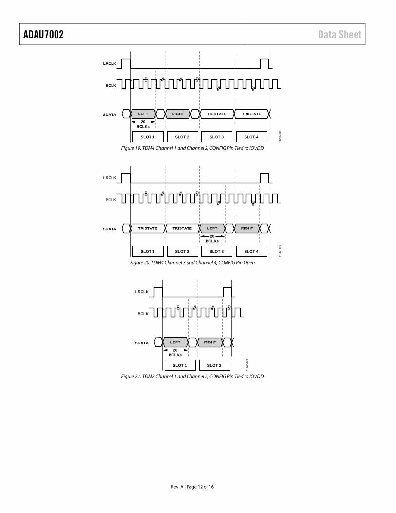
Figure 19. TDM4 Channel 1 and Channel 2, CONFIG Pin Tied to IOVDD
Figure 20. TDM4 Channel 3 and Channel 4, CONFIG Pin Open
Figure 21. TDM2 Channel 1 and Channel 2, CONFIG Pin Tied to IOVDD
SLOT 1
LRCLK
BCLK
SDATA
20BCLKs
RIGHTLEFT
SLOT 2 SLOT 3 SLOT 4
TRISTATE TRISTATE
1126
5-01
9
SLOT 1
LRCLK
BCLK
SDATA
20BCLKs
RIGHTLEFT
SLOT 2 SLOT 3 SLOT 4
TRISTATE TRISTATE
1126
5-02
0
SLOT 1
LRCLK
BCLK
SDATA
20BCLKs
RIGHTLEFT
SLOT 2
1126
5-02
1
Data Sheet ADAU7002
Rev. A | Page 13 of 16
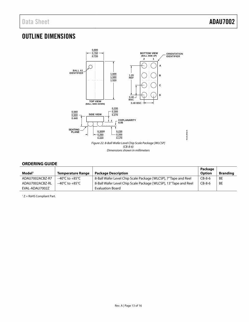
OUTLINE DIMENSIONS
Figure 22. 8-Ball Wafer Level Chip Scale Package [WLCSP]
(CB-8-6) Dimensions shown in millimeters
ORDERING GUIDE
Model1 Temperature Range Package Description PackageOption Branding
ADAU7002ACBZ-R7 −40°C to +85°C 8-Ball Wafer Level Chip Scale Package [WLCSP], 7” Tape and Reel CB-8-6 BE ADAU7002ACBZ-RL −40°C to +85°C 8-Ball Wafer Level Chip Scale Package [WLCSP], 13” Tape and Reel CB-8-6 BE EVAL-ADAU7002Z Evaluation Board 1 Z = RoHS Compliant Part.
01-2
1-20
12-A
A
B
C
D
0.5600.5000.440
0.2300.2000.170
0.3300.3000.270
0.8000.7600.720
1.6001.5601.520
12
BOTTOM VIEW(BALL SIDE UP)
TOP VIEW(BALL SIDE DOWN)
SIDE VIEW
0.30000.2600.220
1.20REF
0.40BSC
0.40 BSC
BALL A1IDENTIFIER
ORIENTATIONIDENTIFIER
SEATINGPLANE
COPLANARITY0.05

ADAU7002 Data Sheet
Rev. A | Page 14 of 16
NOTES

Data Sheet ADAU7002
Rev. A | Page 15 of 16
NOTES

ADAU7002 Data Sheet
Rev. A | Page 16 of 16
NOTES
©2013 Analog Devices, Inc. All rights reserved. Trademarks and registered trademarks are the property of their respective owners. D11265-0-7/13(A)