Stereo 3W Audio Power Amplifiers with Headphone … amplifiers is externally set, allowing maximum...
31
General Description The MAX9760–MAX9763 family combines a stereo or mono 3W bridge-tied load (BTL) audio power amplifier, stereo single-ended headphone amplifier, headphone sensing, and a 2:1 input multiplexer all in a tiny 28-pin thin QFN package. These devices operate from a sin- gle 4.5V to 5.5V supply and feature an industry-leading 100dB PSRR, allowing these devices to operate from noisy supplies without the addition of a linear regulator. An ultra-low 0.002% THD+N ensures clean, low-distor- tion amplification of the audio signal. Click-and-pop suppression eliminates audible transients on power and shutdown cycles. Power-saving features include low 4mV V OS (minimizes DC current drain through the speakers), low 13mA supply current, and a 10μA shut- down mode. A MUTE function allows the outputs to be quickly enabled or disabled. A headphone sense input detects the presence of a headphone jack and automatically configures the amplifiers for either speaker or headphone mode. In speaker mode, the amplifiers can deliver up to 3W of continuous average power into a 3Ω load. In head- phone mode, the amplifier can deliver up to 200mW of continuous average power into a 16Ω load. The gain of the amplifiers is externally set, allowing maximum flexi- bility in optimizing output levels for a given load. The amplifiers also feature a 2:1 input multiplexer, allowing multiple audio sources to be selected. The multiplexer can also be used to compensate for limitations in the frequency response of the loud speakers by selecting an external equalizer network. The various functions are controlled by either an I 2 C-compatible or simple parallel control interface. The MAX9760–MAX9763 are available in either a ther- mally efficient 28-pin thin QFN package (5mm ✕ 5mm ✕ 0.8mm) or a TSSOP-EP package. All devices have ther- mal overload protection (OVP) and are specified over the extended -40°C to +85°C temperature range. Applications Notebooks Portable DVD Players Tablet PCs PC Audio Peripherals Camcorders Features ♦ Industry-Leading, Ultra-High 100dB PSRR ♦ PC99/01 Compliant ♦ 3W BTL Stereo Speaker Amplifier ♦ 200mW Stereo Headphone Amplifier ♦ Low 0.002% THD+N ♦ Click-and-Pop Suppression ♦ ESD-Protected Outputs ♦ Low Quiescent Current: 13mA ♦ Low-Power Shutdown Mode: 10μA ♦ MUTE Function ♦ Headphone Sense Input ♦ Stereo 2:1 Input Multiplexer ♦ Optional 2-Wire, I 2 C-Compatible or Parallel Interface ♦ Tiny 28-Pin Thin QFN (5mm ✕ 5mm ✕ 0.8mm) and TSSOP-EP Packages MAX9760–MAX9763 Stereo 3W Audio Power Amplifiers with Headphone Drive and Input Mux ________________________________________________________________ Maxim Integrated Products 1 SE/ BTL SINGLE SUPPLY 4.5V TO 5.5V I 2 C- COMPATIBLE MAX9760 LEFT IN1 LEFT IN2 RIGHT IN1 RIGHT IN2 CONTROL Simplified Block Diagram Ordering Information 19-2744; Rev 0; 1/03 For pricing, delivery, and ordering information, please contact Maxim/Dallas Direct! at 1-888-629-4642, or visit Maxim’s website at www.maxim-ic.com. PART TEMP RANGE PIN-PACKAGE MAX9760ETI -40°C to +85°C 28 Thin QFN-EP* MAX9760EUI -40°C to +85°C 28 TSSOP-EP* Pin Configurations and Functional Diagrams appear at end of data sheet. Ordering Information continued at end of data sheet. *EP = Exposed paddle.
Transcript of Stereo 3W Audio Power Amplifiers with Headphone … amplifiers is externally set, allowing maximum...

General DescriptionThe MAX9760–MAX9763 family combines a stereo ormono 3W bridge-tied load (BTL) audio power amplifier,stereo single-ended headphone amplifier, headphonesensing, and a 2:1 input multiplexer all in a tiny 28-pinthin QFN package. These devices operate from a sin-gle 4.5V to 5.5V supply and feature an industry-leading100dB PSRR, allowing these devices to operate fromnoisy supplies without the addition of a linear regulator.An ultra-low 0.002% THD+N ensures clean, low-distor-tion amplification of the audio signal. Click-and-popsuppression eliminates audible transients on power andshutdown cycles. Power-saving features include low4mV VOS (minimizes DC current drain through thespeakers), low 13mA supply current, and a 10µA shut-down mode. A MUTE function allows the outputs to bequickly enabled or disabled.
A headphone sense input detects the presence of aheadphone jack and automatically configures theamplifiers for either speaker or headphone mode. Inspeaker mode, the amplifiers can deliver up to 3W ofcontinuous average power into a 3Ω load. In head-phone mode, the amplifier can deliver up to 200mW ofcontinuous average power into a 16Ω load. The gain ofthe amplifiers is externally set, allowing maximum flexi-bility in optimizing output levels for a given load. Theamplifiers also feature a 2:1 input multiplexer, allowingmultiple audio sources to be selected. The multiplexercan also be used to compensate for limitations in thefrequency response of the loud speakers by selectingan external equalizer network. The various functions arecontrolled by either an I2C-compatible or simple parallelcontrol interface.
The MAX9760–MAX9763 are available in either a ther-mally efficient 28-pin thin QFN package (5mm 5mm 0.8mm) or a TSSOP-EP package. All devices have ther-mal overload protection (OVP) and are specified overthe extended -40°C to +85°C temperature range.
ApplicationsNotebooks
Portable DVD Players
Tablet PCs
PC Audio Peripherals
Camcorders
Features♦ Industry-Leading, Ultra-High 100dB PSRR
♦ PC99/01 Compliant
♦ 3W BTL Stereo Speaker Amplifier
♦ 200mW Stereo Headphone Amplifier
♦ Low 0.002% THD+N
♦ Click-and-Pop Suppression
♦ ESD-Protected Outputs
♦ Low Quiescent Current: 13mA
♦ Low-Power Shutdown Mode: 10µA
♦ MUTE Function
♦ Headphone Sense Input
♦ Stereo 2:1 Input Multiplexer
♦ Optional 2-Wire, I2C-Compatible or ParallelInterface
♦ Tiny 28-Pin Thin QFN (5mm 5mm 0.8mm) andTSSOP-EP Packages
MA
X9
76
0–M
AX
97
63
Stereo 3W Audio Power Amplifiers withHeadphone Drive and Input Mux
________________________________________________________________ Maxim Integrated Products 1
SE/BTL
SINGLE SUPPLY4.5V TO 5.5V
I2C-COMPATIBLE
MAX9760
LEFT IN1
LEFT IN2
RIGHT IN1
RIGHT IN2
CONTROL
Simplified Block Diagram
Ordering Information
19-2744; Rev 0; 1/03
For pricing, delivery, and ordering information, please contact Maxim/Dallas Direct! at 1-888-629-4642, or visit Maxim’s website at www.maxim-ic.com.
PART TEMP RANGE PIN-PACKAGE
MAX9760ETI -40°C to +85°C 28 Thin QFN-EP*
MAX9760EUI -40°C to +85°C 28 TSSOP-EP*
Pin Configurations and Functional Diagrams appear at endof data sheet.
Ordering Information continued at end of data sheet.
*EP = Exposed paddle.

MA
X9
76
0–M
AX
97
63
Stereo 3W Audio Power Amplifiers withHeadphone Drive and Input Mux
2 _______________________________________________________________________________________
ABSOLUTE MAXIMUM RATINGS
Stresses beyond those listed under “Absolute Maximum Ratings” may cause permanent damage to the device. These are stress ratings only, and functionaloperation of the device at these or any other conditions beyond those indicated in the operational sections of the specifications is not implied. Exposure toabsolute maximum rating conditions for extended periods may affect device reliability.
VDD to GND ...........................................................................+6VSVDD to GND .........................................................................+6VSVDD to VDD.........................................................................-0.3VPVDD to VDD .......................................................................±0.3VPGND to GND.....................................................................±0.3VAll Other Pins to GND.................................-0.3V to (VDD + 0.3V)Continuous Input Current (into any pin except power-supplyand output pins) ...............................................................±20mA
Continuous Power Dissipation28-Pin Thin QFN (derate 20.8mW/°C above +70°C) ....1667mW28-Pin TSSOP-EP (derate 23.8mW/°C above +70°C) ..1905mW
Operating Temperature Range ...........................-40°C to +85°CStorage Temperature Range .............................-65°C to +150°CJunction Temperature ......................................................+150°CLead Temperature (soldering, 10s) .................................+300°C
ELECTRICAL CHARACTERISTICS(VDD = PVDD = 5.0V, GND = PGND = 0V, SHDN = 5V, CBIAS = 1µF, RIN = RF = 15kΩ, RL = ∞. TA = TMIN to TMAX, unless otherwisenoted. Typical values are at TA = +25°C.) (Note 1)
PARAMETER SYMBOL CONDITIONS MIN TYP MAX UNITS
Supply Voltage Range VDD/PVDD Inferred from PSRR test 4.5 5.5 V
MAX9760/MAX9761 13 32BTL mode,HPS = 0V MAX9762/MAX9763 7 18
Quiescent Supply Current(IVDD + IPVDD)
IDD
Single-ended mode, HPS = VDD 7 18
mA
Shutdown Current I SHDN SHDN = GND 10 50 µA
Switching Time tSW Gain or input switching 10 µs
CBIAS = 1µF 300Turn-On Time tON
CBIAS = 0.1µF 30ms
Thermal Shutdown Threshold 160 oC
Thermal Shutdown Hysteresis 15 oC
OUTPUT AMPLIFIERS (SPEAKER MODE, HPS = GND)
Output Offset Voltage VOS OUT_+ - OUT_-, AV = 1V/V ±4 ±32 mV
VDD = 4.5V to 5.5V 75 100
f = 1kHz, VRIPPLE =200mVP-P
82Power-Supply Rejection Ratio PSRR (Note 2)
f = 20kHz, VRIPPLE =200mVP-P
70
dB
RL = 8Ω 1 1.4
RL = 4Ω 2.6Output Power POUT
fIN = 1kHz,THD+N < 1%,TA = +25°C RL = 3Ω 3
W
POUT = 1W, RL = 8Ω 0.005Total Harmonic Distortion PlusNoise
THD+NfIN = 1kHz, BW =22Hz to 22kHz POUT = 2W, RL = 4Ω 0.01
%
Signal-to-Noise Ratio SNR RL = 8Ω, POUT = 1W, BW = 22Hz to 22kHz 95 dB
Slew Rate SR 1.6 V/µs
Maximum Capacitive Load Drive CL No sustained oscillations 1 nF
Crosstalk fIN = 10kHz 73 dB
MA
X9
76
0–M
AX
97
63
Stereo 3W Audio Power Amplifiers withHeadphone Drive and Input Mux
_______________________________________________________________________________________ 3
ELECTRICAL CHARACTERISTICS (continued)(VDD = PVDD = 5.0V, GND = PGND = 0V, SHDN = 5V, CBIAS = 1µF, RIN = RF = 15kΩ, RL = ∞. TA = TMIN to TMAX, unless otherwisenoted. Typical values are at TA = +25°C.) (Note 1)
PARAMETER SYMBOL CONDITIONS MIN TYP MAX UNITS
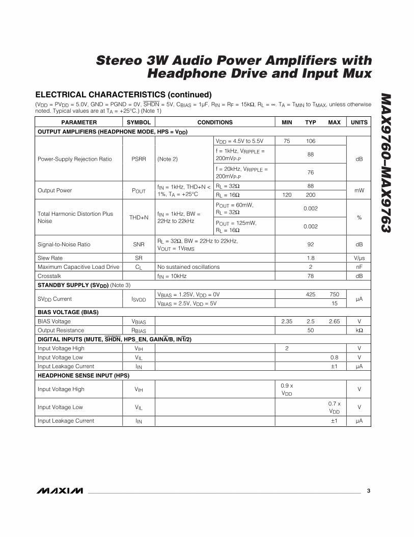
OUTPUT AMPLIFIERS (HEADPHONE MODE, HPS = VDD)
VDD = 4.5V to 5.5V 75 106
f = 1kHz, VRIPPLE =200mVP-P
88Power-Supply Rejection Ratio PSRR (Note 2)
f = 20kHz, VRIPPLE =200mVP-P
76
dB
RL = 32Ω 88Output Power POUT
fIN = 1kHz, THD+N <1%, TA = +25°C RL = 16Ω 120 200
mW
POUT = 60mW,RL = 32Ω
0.002Total Harmonic Distortion PlusNoise
THD+NfIN = 1kHz, BW =22Hz to 22kHz POUT = 125mW,
RL = 16Ω0.002
%
Signal-to-Noise Ratio SNRRL = 32Ω, BW = 22Hz to 22kHz,VOUT = 1VRMS
92 dB
Slew Rate SR 1.8 V/µs
Maximum Capacitive Load Drive CL No sustained oscillations 2 nF
Crosstalk fIN = 10kHz 78 dB
STANDBY SUPPLY (SVDD) (Note 3)
VBIAS = 1.25V, VDD = 0V 425 750SVDD Current ISVDD
VBIAS = 2.5V, VDD = 5V 15µA
BIAS VOLTAGE (BIAS)
BIAS Voltage VBIAS 2.35 2.5 2.65 V
Output Resistance RBIAS 50 kΩDIGITAL INPUTS (MUTE, SHDN, HPS_EN, GAINA/B, IN1111/2)
Input Voltage High VIH 2 V
Input Voltage Low VIL 0.8 V
Input Leakage Current IIN ±1 µA
HEADPHONE SENSE INPUT (HPS)
Input Voltage High VIH0.9 xVDD
V
Input Voltage Low VIL0.7 xVDD
V
Input Leakage Current IIN ±1 µA

MA
X9
76
0–M
AX
97
63
Stereo 3W Audio Power Amplifiers withHeadphone Drive and Input Mux
4 _______________________________________________________________________________________
ELECTRICAL CHARACTERISTICS (continued)(VDD = PVDD = 5.0V, GND = PGND = 0V, SHDN = 5V, CBIAS = 1µF, RIN = RF = 15kΩ, RL = ∞. TA = TMIN to TMAX, unless otherwisenoted. Typical values are at TA = +25°C.) (Note 1)
PARAMETER SYMBOL CONDITIONS MIN TYP MAX UNITS
2-WIRE SERIAL INTERFACE (SCL, SDA, ADD, INT) (MAX9760/MAX9762)
Input Voltage High VIH 2.6 V
Input Voltage Low VIL 0.8 V
Input Hysteresis 0.2 V
Input High Leakage Current IIH VIN = 5V ±1 µA
Input Low Leakage Current IIL VIN = 0V ±1 µA
Input Capacitance CIN 10 pF
Output Voltage Low VOL IOL = 3mA 0.4 V
Output Current High IOH VOH = 5V 1 µA
TIMING CHARACTERISTICS (MAX9760/MAX9762)
Serial Clock Frequency fSCL 400 kHz
Bus Free Time Between STOPand START Conditions
tBUF 1.3 µs
START Condition Hold Time tHD:STA 0.6 µs
START Condition Setup Time tSU:STA 0.6 µs
Clock Period Low tLOW 1.3 µs
Clock Period High tHIGH 0.6 µs
Data Setup Time tSU:DAT 100 ns
Data Hold Time tHD:DAT (Note 4) 0 0.9 µs
Receive SCL/SDA Rise Time tr (Note 5)20 +
0.1CB300 ns
Receive SCL/SDA Fall Time tf (Note 5)20 +
0.1CB300 ns
Transmit SDA Fall Time tf (Note 5)20 +
0.1CB250 ns
Pulse Width of SuppressedSpike
tSP (Note 6) 50 ns
Note 1: All devices are 100% production tested at +25°C. All temperature limits are guaranteed by design.Note 2: PSRR is specified with the amplifier inputs connected to GND through RIN and CIN.Note 3: Refer to the SVDD section.Note 4: A master device must provide a hold time of at least 300ns for the SDA signal to bridge the undefined region of SCL’s falling
edge.Note 5: CB = total capacitance of one of the bus lines in picofarads. Device tested with CB = 400pF. 1kΩ pullup resistors connected
from SDA/SCL to VDD. Note 6: Input filters on SDA, SCL, and ADD suppress noise spikes of less than 50ns.

MA
X9
76
0–M
AX
97
63
Stereo 3W Audio Power Amplifiers withHeadphone Drive and Input Mux
_______________________________________________________________________________________ 5
TOTAL HARMONIC DISTORTION PLUS NOISEvs. FREQUENCY (SPEAKER MODE)
MAX
9760
toc0
1
FREQUENCY (Hz)
THD+
N (%
)
10k1k100
0.01
0.1
1
0.00110 100k
RL = 3ΩAV = 2V/V
POUT = 2.5WPOUT = 2W
POUT = 500mW POUT = 1W
TOTAL HARMONIC DISTORTION PLUS NOISEvs. FREQUENCY (SPEAKER MODE)
MAX
9760
toc0
2
FREQUENCY (Hz)
THD+
N (%
)
10k1k100
0.01
0.1
1
0.00110 100k
RL = 3ΩAV = 4V/V
POUT = 2.5WPOUT = 2W
POUT = 500mW POUT = 1W
TOTAL HARMONIC DISTORTION PLUS NOISEvs. FREQUENCY (SPEAKER MODE)
MAX
9760
toc0
3
FREQUENCY (Hz)
THD+
N (%
)
10k1k100
0.01
0.1
1
0.00110 100k
RL = 4ΩAV = 2V/V
POUT = 2WPOUT = 1W
POUT = 500mWPOUT = 250mW
TOTAL HARMONIC DISTORTION PLUS NOISEvs. FREQUENCY (SPEAKER MODE)
MAX
9760
toc0
4
FREQUENCY (Hz)
THD+
N (%
)
10k1k100
0.01
0.1
1
0.00110 100k
RL = 4ΩAV = 4V/V
POUT = 250mW
POUT = 2WPOUT = 1W
POUT = 500mW
TOTAL HARMONIC DISTORTION PLUS NOISEvs. FREQUENCY (SPEAKER MODE)
MAX
9760
toc0
5
FREQUENCY (Hz)
THD+
N (%
)
10k1k100
0.01
0.1
1
0.00110 100k
RL = 8ΩAV = 2V/V
POUT = 250mW
POUT = 1.2WPOUT = 1W
POUT = 500mW
TOTAL HARMONIC DISTORTION PLUS NOISEvs. FREQUENCY (SPEAKER MODE)
MAX
9760
toc0
6
FREQUENCY (Hz)
THD+
N (%
)
10k1k100
0.01
0.1
1
0.00110 100k
POUT = 250mW
POUT = 1.2WPOUT = 1W
POUT = 500mW
RL = 8ΩAV = 4V/V
TOTAL HARMONIC DISTORTION PLUS NOISEvs. OUTPUT POWER (SPEAKER MODE)
MAX
9760
toc0
7
OUTPUT POWER (W)
THD+
N (%
)
321
0.01
10
1
0.1
100
0.0010 4
AV = 2V/VRL = 3Ω
f = 1kHz
f = 20Hzf = 10kHz
TOTAL HARMONIC DISTORTION PLUS NOISEvs. OUTPUT POWER (SPEAKER MODE)
MAX
9760
toc0
8
OUTPUT POWER (W)
THD+
N (%
)
321
0.01
10
1
0.1
100
0.0010 4
AV = 4V/VRL = 3Ω
f = 20Hz
f = 1kHz
f = 10kHz
TOTAL HARMONIC DISTORTION PLUS NOISEvs. OUTPUT POWER (SPEAKER MODE)
MAX
9760
toc0
9
OUTPUT POWER (W)
THD+
N (%
)
2.5 3.02.01.51.00.5
0.01
10
1
0.1
100
0.0010 3.5
AV = 2V/VRL = 4Ω
f = 20Hz
f = 1kHzf = 10kHz
Typical Operating Characteristics(VDD = PVDD = 5V, TA = +25°C, unless otherwise noted.)

MA
X9
76
0–M
AX
97
63
Stereo 3W Audio Power Amplifiers withHeadphone Drive and Input Mux
6 _______________________________________________________________________________________
TOTAL HARMONIC DISTORTION PLUS NOISEvs. OUTPUT POWER (SPEAKER MODE)
MAX
9760
toc1
0
OUTPUT POWER (W)
THD+
N (%
)
2.5 3.02.01.51.00.5
0.01
10
1
0.1
100
0.0010 3.5
AV = 4V/VRL = 4Ω
f = 20Hz
f = 1kHz
f = 10kHz
TOTAL HARMONIC DISTORTION PLUS NOISEvs. OUTPUT POWER (SPEAKER MODE)
MAX
9760
toc1
1
OUTPUT POWER (W)
THD+
N (%
)
1.51.00.5
0.01
10
1
0.1
100
0.0010 2.0
AV = 2V/VRL = 8Ω
f = 20Hz
f = 1kHz
f = 10kHz
TOTAL HARMONIC DISTORTION PLUS NOISEvs. OUTPUT POWER (SPEAKER MODE)
MAX
9760
toc1
2
OUTPUT POWER (W)
THD+
N (%
)
1.51.00.5
0.01
10
1
0.1
100
0.0010 2.0
AV = 4V/VRL = 8Ω
f = 20Hz
f = 1kHz
f = 10kHz
OUTPUT POWER vs. TEMPERATURE(SPEAKER MODE)
MAX
9760
toc1
3
TEMPERATURE (°C)
OUTP
UT P
OWER
(W)
603510-15
1
2
3
4
0-40 85
THD+N = 10%
THD+N = 1%
f = 1kHzRL = 3Ω
OUTPUT POWER vs. TEMPERATURE(SPEAKER MODE)
MAX
9760
toc1
4
TEMPERATURE (°C)
OUTP
UT P
OWER
(W)
603510-15
1
2
3
4
0-40 85
THD+N = 10%
THD+N = 1%
f = 1kHzRL = 4Ω
OUTPUT POWER vs. TEMPERATURE(SPEAKER MODE)
MAX
9760
toc1
5
TEMPERATURE (°C)
OUTP
UT P
OWER
(W)
603510-15
0.5
1.0
1.5
2.0
0-40 85
THD+N = 10%
THD+N = 1%
f = 1kHzRL = 8Ω
OUTPUT POWER vs. LOAD RESISTANCE(SPEAKER MODE)
MAX
9760
toc1
6
LOAD RESISTANCE (Ω)
OUTP
UT P
OWER
(W)
10k1k10010
1
2
3
4
5
01 100k
f = 1kHz
THD+N = 10%
THD+N = 1%
POWER DISSIPATION vs. OUTPUT POWER(SPEAKER MODE)
MAX
9760
toc1
7
OUTPUT POWER (W)
POW
ER D
ISSI
PATI
ON (W
)
2.50.5 1.0 1.5 2.0
0.2
0.4
0.6
0.8
1.0
1.2
1.4
1.6
00
RL = 4Ωf = 1kHz
Typical Operating Characteristics (continued)(VDD = PVDD = 5V, TA = +25°C, unless otherwise noted.)

MA
X9
76
0–M
AX
97
63
Stereo 3W Audio Power Amplifiers withHeadphone Drive and Input Mux
_______________________________________________________________________________________ 7
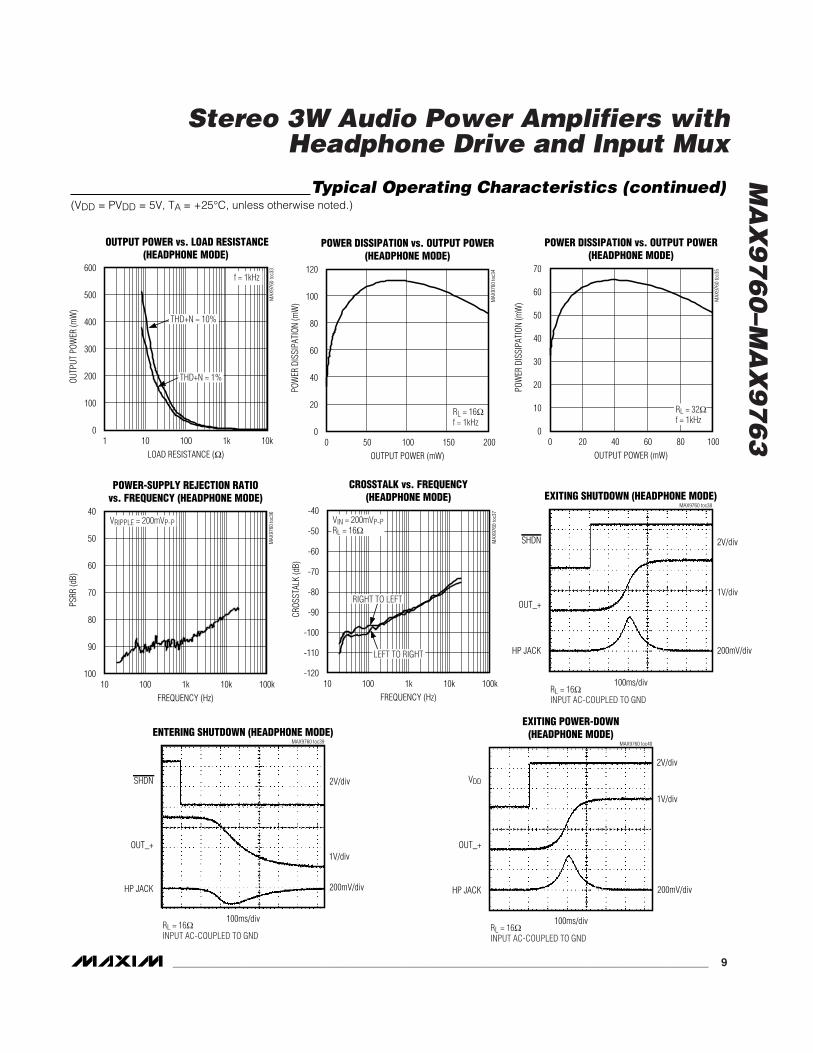
CROSSTALK vs. FREQUENCY(SPEAKER MODE)
MAX
9760
toc1
9
FREQUENCY (Hz)
CROS
STAL
K (d
B)
10k1k100
-110
-100
-90
-80
-70
-60
-50
-40
-12010 100k
VIN = 200mVP-PRL = 8Ω
RIGHT TO LEFT
LEFT TO RIGHT
ENTERING SHUTDOWN (SPEAKER MODE)MAX9760 toc20
100ms/div
OUT_+AND OUT_-
2V/div
1V/div
200mV/divOUT_+- OUT_-
SHDN
RL = 8ΩINPUT AC-COUPLED TO GND
EXITING SHUTDOWN (SPEAKER MODE)MAX9760 toc21
100ms/div
OUT_+AND OUT_-
2V/div
1V/div
200mV/divOUT_+
- OUT_-
SHDN
RL = 8ΩINPUT AC-COUPLED TO GND
ENTERING POWER-DOWN(SPEAKER MODE)
MAX9760 toc22
100ms/div
OUT_+AND OUT_-
2V/div
1V/div
200mV/divOUT_+
- OUT_-
VDD
RL = 8ΩINPUT AC-COUPLED TO GND
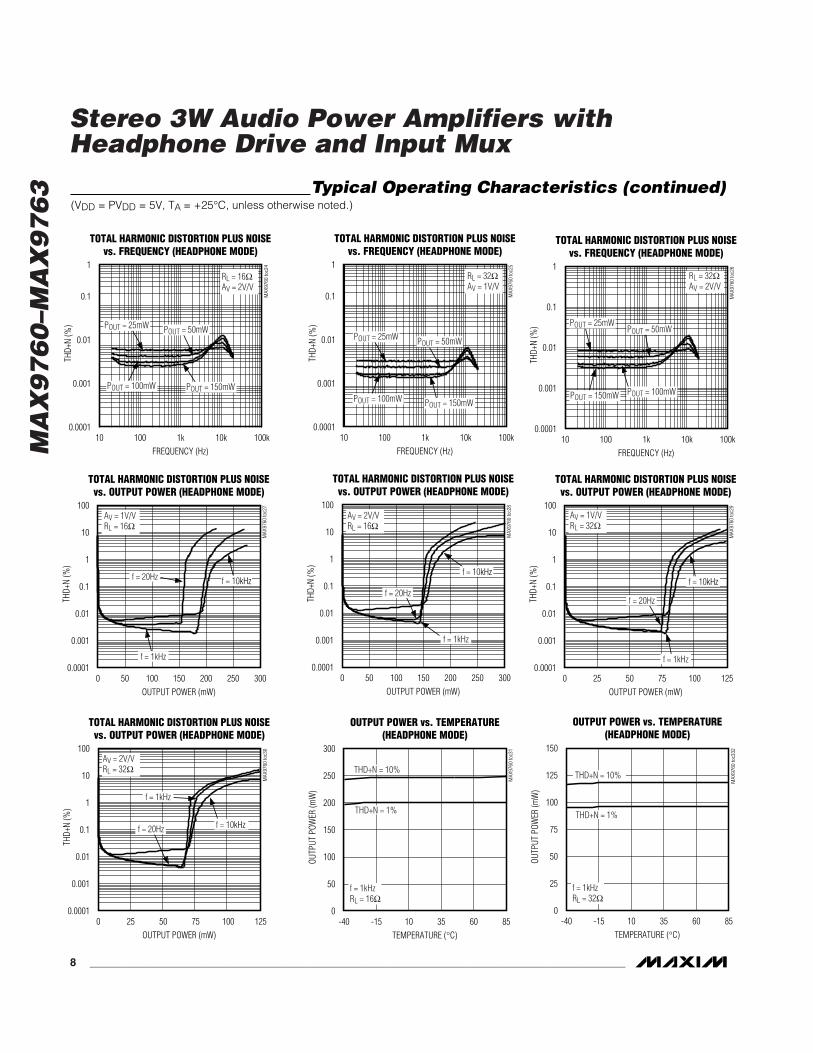
TOTAL HARMONIC DISTORTION PLUS NOISEvs. FREQUENCY (HEADPHONE MODE)
MAX
9760
toc2
3
FREQUENCY (Hz)
THD+
N (%
)
10k1k100
0.001
0.01
0.1
1
0.000110 100k
RL = 16ΩAV = 1V/V
POUT = 50mWPOUT = 25mW
POUT = 100mWPOUT = 150mW
Typical Operating Characteristics (continued)(VDD = PVDD = 5V, TA = +25°C, unless otherwise noted.)
POWER-SUPPLY REJECTION RATIOvs. FREQUENCY (SPEAKER MODE)
MAX
9760
toc1
8
FREQUENCY (Hz)
PSRR
(dB)
10k1k100
90
80
70
60
50
40
10010 100k
VRIPPLE = 200mVP-P
MA
X9
76
0–M
AX
97
63
Stereo 3W Audio Power Amplifiers withHeadphone Drive and Input Mux
8 _______________________________________________________________________________________
TOTAL HARMONIC DISTORTION PLUS NOISEvs. OUTPUT POWER (HEADPHONE MODE)
MAX
9760
toc2
8
OUTPUT POWER (mW)
THD+
N (%
)
25020015010050
0.01
0.001
10
1
0.1
100
0.00010 300
AV = 2V/VRL = 16Ω
f = 20Hz
f = 1kHz
f = 10kHz
TOTAL HARMONIC DISTORTION PLUS NOISEvs. OUTPUT POWER (HEADPHONE MODE)
MAX
9760
toc2
9
OUTPUT POWER (mW)
THD+
N (%
)
100755025
0.01
0.001
10
1
0.1
100
0.00010 125
AV = 1V/VRL = 32Ω
f = 20Hz
f = 1kHz
f = 10kHz
TOTAL HARMONIC DISTORTION PLUS NOISEvs. OUTPUT POWER (HEADPHONE MODE)
MAX
9760
toc3
0
OUTPUT POWER (mW)
THD+
N (%
)
100755025
0.01
0.001
10
1
0.1
100
0.00010 125
AV = 2V/VRL = 32Ω
f = 20Hz
f = 1kHz
f = 10kHz
OUTPUT POWER vs. TEMPERATURE(HEADPHONE MODE)
MAX
9760
toc3
1
TEMPERATURE (°C)
OUTP
UT P
OWER
(mW
)
603510-15
50
100
200
150
250
300
0-40 85
THD+N = 10%
THD+N = 1%
f = 1kHzRL = 16Ω
OUTPUT POWER vs. TEMPERATURE(HEADPHONE MODE)
MAX
9760
toc3
32
TEMPERATURE (°C)
OUTP
UT P
OWER
(mW
)
603510-15
25
50
100
75
125
150
0-40 85
THD+N = 10%
THD+N = 1%
f = 1kHzRL = 32Ω
Typical Operating Characteristics (continued)(VDD = PVDD = 5V, TA = +25°C, unless otherwise noted.)
TOTAL HARMONIC DISTORTION PLUS NOISEvs. FREQUENCY (HEADPHONE MODE)
MAX
9760
toc2
5
FREQUENCY (Hz)
THD+
N (%
)
10k1k100
0.001
0.01
0.1
1
0.000110 100k
RL = 32ΩAV = 1V/V
POUT = 50mWPOUT = 25mW
POUT = 100mW POUT = 150mW
TOTAL HARMONIC DISTORTION PLUS NOISEvs. FREQUENCY (HEADPHONE MODE)
MAX
9760
toc2
6
FREQUENCY (Hz)
THD+
N (%
)
10k1k100
0.001
0.01
0.1
1
0.000110 100k
RL = 32ΩAV = 2V/V
POUT = 50mWPOUT = 25mW
POUT = 100mWPOUT = 150mW
TOTAL HARMONIC DISTORTION PLUS NOISEvs. OUTPUT POWER (HEADPHONE MODE)
MAX
9760
toc2
7
OUTPUT POWER (mW)
THD+
N (%
)
25020015010050
0.01
0.001
10
1
0.1
100
0.00010 300
AV = 1V/VRL = 16Ω
f = 20Hz
f = 1kHz
f = 10kHz
TOTAL HARMONIC DISTORTION PLUS NOISEvs. FREQUENCY (HEADPHONE MODE)
MAX
9760
toc2
4
FREQUENCY (Hz)
THD+
N (%
)
10k1k100
0.001
0.01
0.1
1
0.000110 100k
RL = 16ΩAV = 2V/V
POUT = 50mWPOUT = 25mW
POUT = 100mW POUT = 150mW
MA
X9
76
0–M
AX
97
63
Stereo 3W Audio Power Amplifiers withHeadphone Drive and Input Mux
_______________________________________________________________________________________ 9
CROSSTALK vs. FREQUENCY(HEADPHONE MODE)
MAX
9760
toc3
7
FREQUENCY (Hz)
CROS
STAL
K (d
B)
10k1k100
-110
-100
-90
-80
-70
-60
-50
-40
-12010 100k
VIN = 200mVP-PRL = 16Ω
RIGHT TO LEFT
LEFT TO RIGHT
EXITING SHUTDOWN (HEADPHONE MODE)MAX9760 toc38
100ms/div
OUT_+
2V/div
1V/div
200mV/divHP JACK
SHDN
RL = 16ΩINPUT AC-COUPLED TO GND
ENTERING SHUTDOWN (HEADPHONE MODE)MAX9760 toc39
100ms/div
OUT_+
2V/div
1V/div
200mV/divHP JACK
SHDN
RL = 16ΩINPUT AC-COUPLED TO GND
EXITING POWER-DOWN(HEADPHONE MODE)
MAX9760 toc40
100ms/div
OUT_+
2V/div
1V/div
200mV/divHP JACK
VDD
RL = 16ΩINPUT AC-COUPLED TO GND
Typical Operating Characteristics (continued)(VDD = PVDD = 5V, TA = +25°C, unless otherwise noted.)
POWER DISSIPATION vs. OUTPUT POWER(HEADPHONE MODE)
MAX
9760
toc3
5
OUTPUT POWER (mW)
POW
ER D
ISSI
PATI
ON (m
W)
10020 40 60 80
10
20
30
40
50
60
70
00
RL = 32Ωf = 1kHz
POWER-SUPPLY REJECTION RATIOvs. FREQUENCY (HEADPHONE MODE)
MAX
9760
toc3
6
FREQUENCY (Hz)
PSRR
(dB)
10k1k100
90
80
70
60
50
40
10010 100k
VRIPPLE = 200mVP-P
OUTPUT POWER vs. LOAD RESISTANCE(HEADPHONE MODE)
MAX
9760
toc3
3
LOAD RESISTANCE (Ω)
OUTP
UT P
OWER
(mW
)
1k10010
100
200
300
400
500
600
01 10k
f = 1kHz
THD+N = 10%
THD+N = 1%
POWER DISSIPATION vs. OUTPUT POWER(HEADPHONE MODE)
MAX
9760
toc3
4
OUTPUT POWER (mW)
POW
ER D
ISSI
PATI
ON (m
W)
50 100 150 200
20
40
60
80
100
120
00
RL = 16Ωf = 1kHz

MA
X9
76
0–M
AX
97
63
Stereo 3W Audio Power Amplifiers withHeadphone Drive and Input Mux
10 ______________________________________________________________________________________
EXITING POWER-DOWN(SPEAKER MODE)
MAX9760 toc46
100ms/div
OUT_+AND OUT_-
2V/div
1V/div
200mV/divOUT_+- OUT_-
VDD
RL = 8ΩINPUT AC-COUPLED TO GND
Typical Operating Characteristics (continued)(VDD = PVDD = 5V, TA = +25°C, unless otherwise noted.)
ENTERING POWER-DOWN(HEADPHONE MODE)
MAX9760 toc41
100ms/div
OUT_+
2V/div
1V/div
200mV/divHP JACK
VDD
RL = 16ΩINPUT AC-COUPLED TO GND
SUPPLY CURRENT vs. SUPPLY VOLTAGE(SPEAKER MODE)
MAX
9760
toc4
2
SUPPLY VOLTAGE (V)SU
PPLY
CUR
RENT
(mA)
5.255.004.75
5
10
15
20
25
04.50 5.50
TA = +85°C
TA = +25°C
TA = -40°C
SUPPLY CURRENT vs. SUPPLY VOLTAGE(HEADPHONE MODE)
MAX
9760
toc4
3
SUPPLY VOLTAGE (V)
SUPP
LY C
URRE
NT (m
A)
5.255.004.75
2
4
6
8
10
12
04.50 5.50
TA = +85°C
TA = +25°C
TA = -40°C
SHUTDOWN SUPPLY CURRENTvs. SUPPLY VOLTAGE
MAX
9796
0 to
c44
SUPPLY VOLTAGE (V)
SUPP
LY C
URRE
NT (µ
A)
5.255.004.75
5
10
15
20
04.50 5.50
TA = +85°CTA = +25°C
TA = -40°C
POWER DISSIPATION vs. OUTPUT POWER(SPEAKER MODE)
MAX
9760
toc4
5
OUTPUT POWER (W)
POW
ER D
ISSI
PATI
ON (W
)
1.500.25 0.50 0.75 1.00 1.25
0.1
0.2
0.3
0.4
0.5
0.6
0.7
0.8
00
RL = 8Ωf = 1kHz

MA
X9
76
0–M
AX
97
63
Stereo 3W Audio Power Amplifiers withHeadphone Drive and Input Mux
______________________________________________________________________________________ 11
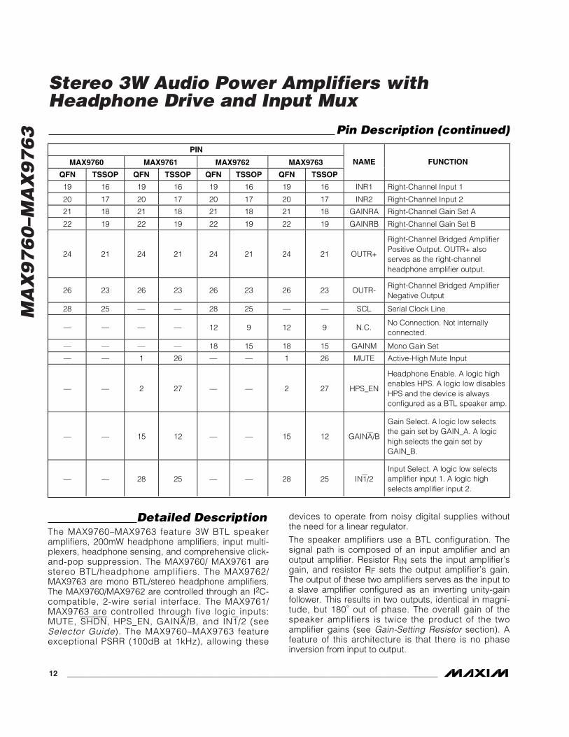
Pin Description
PIN
MAX9760 MAX9761 MAX9762 MAX9763
QFN TSSOP QFN TSSOP QFN TSSOP QFN TSSOP
NAME FUNCTION
1 26 — — 1 26 — — SDA Bidirectional Serial Data I/O
2 27 — — 2 27 — — INT µC Interrupt Output
3 28 3 28 3 28 3 28 VDD Power Supply
4 1 4 1 4 1 4 1 SVDD
Standby Power Supply. Connectto a standby power supply that isalways on, or connect to VDDthrough a Schottky diode andbypass with 220µF capacitor toGND. Short to VDD if clicklessoperation is not essential.
5 2 5 2 5 2 5 2 INL1 Left-Channel Input 1
6 3 6 3 6 3 6 3 INL2 Left-Channel Input 2
7 4 7 4 7 4 7 4 GAINLA Left-Channel Gain Set A
8 5 8 5 8 5 8 5 GAINLB Left-Channel Gain Set B
9, 13,23, 27
6, 10,20, 24
9, 13,23, 27
6, 10, 20,24
9, 23,27
6, 20, 24 9, 23, 27 6, 20, 24 PGND Power Ground
10 7 10 7 10 7 10 7 OUTL+
Left-Channel Bridged AmplifierPositive Output. OUTL+ alsoserves as the left-channelheadphone amplifier output.
11, 25 8, 22 11, 25 8, 22 11, 25 8, 22 11, 25 8, 22 PVDD Output Amplifier Power Supply
12 9 12 9 — — — — OUTL-Left-Channel Bridged AmplifierNegative Output
14 11 14 11 14 11 14 11 SHDNActive-Low Shutdown. ConnectSHDN to VDD for normal operation.
15 12 — — 15 12 — — ADDAddress Select. A logic high setsthe address LSB to 1, a logic lowsets the address LSB to zero.
16 13 16 13 16 13 16 13 HPS
Headphone Sense Input. A logichigh configures the device as asingle-ended headphone amp. Alogic low configures the device asa BTL speaker amp.
17 14 17 14 17 14 17 14 BIAS
DC Bias Bypass. See BIASCapacitor Selection section forcapacitor selection. ConnectCBIAS from BIAS to GND.
18 15 18 15 13 10 13 10 GND Ground
MA
X9
76
0–M
AX
97
63
Stereo 3W Audio Power Amplifiers withHeadphone Drive and Input Mux
12 ______________________________________________________________________________________
Detailed DescriptionThe MAX9760–MAX9763 feature 3W BTL speakeramplifiers, 200mW headphone amplifiers, input multi-plexers, headphone sensing, and comprehensive click-and-pop suppression. The MAX9760/ MAX9761 arestereo BTL/headphone amplifiers. The MAX9762/MAX9763 are mono BTL/stereo headphone amplifiers.The MAX9760/MAX9762 are controlled through an I2C-compatible, 2-wire serial interface. The MAX9761/MAX9763 are controlled through five logic inputs:MUTE, SHDN, HPS_EN, GAINA/B, and IN1/2 (seeSelector Guide). The MAX9760–MAX9763 featureexceptional PSRR (100dB at 1kHz), allowing these
devices to operate from noisy digital supplies withoutthe need for a linear regulator.
The speaker amplifiers use a BTL configuration. Thesignal path is composed of an input amplifier and anoutput amplifier. Resistor RIN sets the input amplifier’sgain, and resistor RF sets the output amplifier’s gain.The output of these two amplifiers serves as the input toa slave amplifier configured as an inverting unity-gainfollower. This results in two outputs, identical in magni-tude, but 180° out of phase. The overall gain of thespeaker amplifiers is twice the product of the twoamplifier gains (see Gain-Setting Resistor section). Afeature of this architecture is that there is no phaseinversion from input to output.
Pin Description (continued)
PIN
MAX9760 MAX9761 MAX9762 MAX9763
QFN TSSOP QFN TSSOP QFN TSSOP QFN TSSOP
NAME FUNCTION
19 16 19 16 19 16 19 16 INR1 Right-Channel Input 1
20 17 20 17 20 17 20 17 INR2 Right-Channel Input 2
21 18 21 18 21 18 21 18 GAINRA Right-Channel Gain Set A
22 19 22 19 22 19 22 19 GAINRB Right-Channel Gain Set B
24 21 24 21 24 21 24 21 OUTR+
Right-Channel Bridged AmplifierPositive Output. OUTR+ alsoserves as the right-channelheadphone amplifier output.
26 23 26 23 26 23 26 23 OUTR-Right-Channel Bridged AmplifierNegative Output
28 25 — — 28 25 — — SCL Serial Clock Line
— — — — 12 9 12 9 N.C.No Connection. Not internallyconnected.
— — — — 18 15 18 15 GAINM Mono Gain Set
— — 1 26 — — 1 26 MUTE Active-High Mute Input
— — 2 27 — — 2 27 HPS_EN
Headphone Enable. A logic highenables HPS. A logic low disablesHPS and the device is alwaysconfigured as a BTL speaker amp.
— — 15 12 — — 15 12 GAINA/B
Gain Select. A logic low selectsthe gain set by GAIN_A. A logichigh selects the gain set byGAIN_B.
— — 28 25 — — 28 25 IN1/2Input Select. A logic low selectsamplifier input 1. A logic highselects amplifier input 2.
MA
X9
76
0–M
AX
97
63
Stereo 3W Audio Power Amplifiers withHeadphone Drive and Input Mux
______________________________________________________________________________________ 13
When configured as a headphone (single-ended) ampli-fier, the slave amplifier is disabled, muting the speakerand the main amplifier drives the headphone. TheMAX9760–MAX9763 can deliver 3W of continuous aver-age power into a 3Ω load with less than 1% THD+N inspeaker mode, and 200mW of continuous averagepower into a 16Ω load with less than 1% THD+N inheadphone mode. These devices also feature thermaloverload protection.
Mono ModeThe MAX9762/MAX9763 are 3W mono speaker ampli-fiers, 200mW stereo headphone amplifiers, and amixer/attenuator (see the MAX9762/MAX9763 FunctionalDiagram). In speaker (mono) mode, the mixer/attenuatorcombines the two stereo inputs (INL_ and INR_) andattenuates the resultant signal by a factor of 2. Thisallows for full reproduction of a stereo signal through asingle speaker, while maintaining optimum headroom.The resistor connected between GAINM and OUTR+,sets the gain of the devices in speaker mode (see theMAX9762 Functional Diagram). This allows the speakeramplifier to have a different gain and feedback networkfrom the headphone amplifier.
BIASThese devices operate from a single 5V supply, andfeature an internally generated, power-supply indepen-dent, common-mode bias voltage of 2.5V referenced toGND. BIAS provides both click-and-pop suppressionand sets the DC bias level for the audio outputs. BIASis internally connected to the noninverting input of eachspeaker amplifier (see Typical Application Circuit/Functional Diagram). Choose the value of the bypasscapacitor as described in the BIAS Capacitor section.No external load should be applied to BIAS. Any loadlowers the BIAS voltage, affecting the overall perfor-mance of the device.
Input MultiplexerEach amplifier features a 2:1 input multiplexer, allowinginput selection between two stereo sources. Both multi-plexers are controlled by bit 1 in the control register(MAX9760/MAX9762) or by the IN1/2 pin (MAX9761/MAX9763). A logic low selects input IN_1 and a logichigh selects input IN_2.
The input multiplexer can also be used to furtherexpand the number of gain options available from theMAX9760–MAX9763 family. Connecting the audiosource to the device through two different input resis-tors (Figure 1) increases the number of gain optionsfrom two to four (MAX9760/MAX9761) and from three tosix (MAX9762/MAX9763). Additionally, the input multi-plexer allows a speaker equalization network to beswitched into the speaker signal path. This is typicallyuseful in optimizing acoustic response from speakerswith small physical dimensions.
Headphone Sense Enable The HPS pin is enabled by HPS_EN (MAX9762/MAX9763) or the HPSD bit (MAX9760/MAX9761).HPSD or HPS_EN determines whether the device is inautomatic detection mode or fixed mode operation (seeTables 1a and 1b).
Headphone Sense Input (HPS)A voltage on HPS less than 0.7 VDD sets the deviceto speaker mode. A voltage greater than 0.9 VDD dis-ables the inverting bridge amplifier (OUT_-), whichmutes the speaker amplifier and sets the device intoheadphone mode.
For automatic headphone detection, connect HPS to thecontrol pin of a 3-wire headphone jack as shown inFigure 2. With no headphone present, the resistive volt-age-divider created by R1 and R2 sets the voltage onHPS to be less than 0.7 VDD, setting the device tospeaker mode and the gain setting defaults to GAINA(MAX9760/MAX9762). When a headphone plug is insert-ed into the jack, the control pin is disconnected from thetip contact, and HPS is pulled to VDD through R1, settingthe device into headphone mode and the gain-settingdefaults to GAINB (MAX9760/MAX9762) (see GainSelect section). Place a resistor in series with the controlpin and HPS (R3) to prevent any audio signal from cou-pling into HPS when the device is in speaker mode.
ShutdownThe MAX9760–MAX9763 feature a 10µA, low-powershutdown mode that reduces quiescent current con-sumption and extends battery life. The drive amplifiersand bias circuitry are disabled, the amplifier outputs(OUT_) go high impedance, and BIAS is driven to
MAX9760
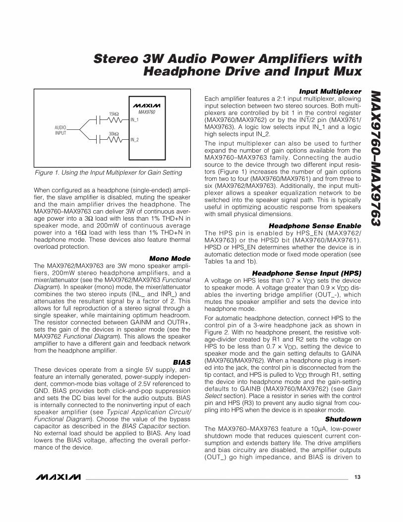
AUDIOINPUT
15kΩ
30kΩ
IN_1
IN_2
Figure 1. Using the Input Multiplexer for Gain Setting

MA
X9
76
0–M
AX
97
63
Stereo 3W Audio Power Amplifiers withHeadphone Drive and Input Mux
14 ______________________________________________________________________________________
GND. Driving SHDN low places the devices into shut-down mode, disables the interface, and resets the I2Cregisters to a default state. A logic high on SHDNenables the devices.
MAX9760/MAX9762 Software ShutdownA logic high on bit 0 of the SHDN register places theMAX9760/MAX9762 in shutdown mode. A logic lowenables the device. The digital section of theMAX9760/MAX9762 remains active when the device isshut down through the interface. All devices feature alogic low on the SHDN input.
MUTEAll devices feature a mute mode. When the device ismuted, the input is disconnected from the amplifiers.MUTE does not shut down the device.
MAX9760/MAX9762 MUTEThe MAX9760/MAX9762 MUTE mode is selected bywriting to the MUTE register (see the Command ByteDefinitions section). The left and right channels can beindependently muted.
MAX9761/MAX9763 MUTEThe MAX9761/MAX9763 feature an active-high MUTEinput that mutes both channels.
Click-and-Pop SuppressionThe MAX9760–MAX9763 feature Maxim’s comprehen-sive click-and-pop suppression. During startup andshutdown, the common-mode bias voltage of the ampli-fiers is slowly ramped to and from the DC bias pointusing an S-shaped waveform. In headphone mode, thiswaveform shapes the frequency spectrum, minimizingthe amount of audible components present at the head-phone. In speaker mode, the BTL amplifiers start up inthe same fashion as in headphone mode. When enter-ing shutdown, both amplifier outputs ramp to GNDquickly and simultaneously. The MAX9760–MAX9763 can also be connected to a standby powersource that ensures that the device undergoes its fullshutdown cycle even after power has been removed.
Standby Power Supply (SVDD)The MAX9760–MAX9763 feature a system that providesclickless power-down when power is inadvertentlyremoved from the device. SVDD is an optional sec-ondary supply that powers the device through its shut-down cycle when VDD is removed. During this cycle,the amplifier output DC level slowly ramps to GND,ensuring clickless power-down. If clickless power-downis required, connect SVDD to either a secondary powersupply that is always on, or connect a reservoir capaci-tor from SVDD to GND. SVDD does not need to be con-
nected to either a secondary power supply or reservoircapacitor for normal device operation. If click-and-popsuppression during power-down is not required, con-nect SVDD to VDD directly.
MAX9760–MAX9763
R347kΩ
R1680kΩ
R210kΩ
HPS
VDD
OUTL+
OUTR+
Figure 2. HPS Configuration Circuit
INPUTS
HPSD HPS SPKR/HPMODE
MAX9760GAINPATH*
MAX9762GAIN
PATH*
0 0 X BTL A M
0 1 X SE B B
1 X 0 BTL A or B M
1 X 1 SE A or B A or B
Table 1a. HPS Setting (MAX9760/MAX9761)
INPUTS
HPSEN HPS
MODEMAX9761
GAIN PATH*MAX9763
GAIN PATH*
0 X BTL A or B M
1 0 BTL A or B M
1 1 SE A or B A or B
Table 1b. HPS Setting (MAX9762/MAX9763)
*Note:A – GAINA path selectedB – GAINB path selectedM – GAINM path selectedA or B – Gain path selected by GAINAB control bit in register02h
*Note:A or B – Gain path selected by external GAINABM – GAINM path selected

MA
X9
76
0–M
AX
97
63
Stereo 3W Audio Power Amplifiers withHeadphone Drive and Input Mux
______________________________________________________________________________________ 15
The clickless power-down cycle only occurs when thedevice is in headphone mode. The speaker mode isinherently clickless, the differential architecture cancelsthe DC shift across the speaker. The MAX9760–MAX9763 BTL outputs are pulled to GND quickly andsimultaneously, resulting in no audible components. Ifthe MAX9760–MAX9763 are only used as speakeramplifiers, then reservoir capacitors or secondary sup-plies are not necessary.
When using a reservoir capacitor, a 220µF capacitorprovides optimum charge storage for the shutdowncycle for all conditions. If a smaller reservoir capacitoris desired, decrease the size of CBIAS. A smaller CBIAScauses the output DC level to decay at a faster rate,increasing the audible content at the speaker, butreducing the duration of the shutdown cycle.
Digital InterfaceThe MAX9760/MAX9762 feature an I2C/SMBus-compat-ible 2-wire serial interface consisting of a serial dataline (SDA) and a serial clock line (SCL). SDA and SCLfacilitate bidirectional communication between theMAX9760/MAX9762 and the master at clock rates up to400kHz. Figure 3 shows the 2-wire interface timing dia-gram. The MAX9760/MAX9762 are transmit/receiveslave-only devices, relying upon a master to generate aclock signal. The master (typically a microcontroller) ini-tiates data transfer on the bus and generates SCL topermit that transfer.
A master device communicates to the MAX9760/MAX9762 by transmitting the proper address followedby a command and/or data words. Each transmitsequence is framed by a START (S) or REPEATEDSTART (Sr) condition and a STOP (P) condition. Eachword transmitted over the bus is 8 bits long and isalways followed by an acknowledge clock pulse.
The MAX9760/MAX9762 SDA and SCL amplifiers areopen-drain outputs requiring a pullup resistor (500Ω orgreater) to generate a logic high voltage. Series resis-tors in line with SDA and SCL are optional. These seriesresistors protect the input stages of the devices fromhigh-voltage spikes on the bus lines, and minimizecrosstalk and undershoot of the bus signals.
Bit TransferOne data bit is transferred during each SCL clockcycle. The data on SDA must remain stable during thehigh period of the SCL clock pulse. Changes in SDAwhile SCL is high are control signals (see START andSTOP Conditions section). SDA and SCL idle highwhen the I2C bus is not busy.
START and STOP ConditionsWhen the serial interface is inactive, SDA and SCL idlehigh. A master device initiates communication by issu-ing a START condition. A START condition is a high-to-low transition on SDA with SCL high. A STOP conditionis a low-to-high transition on SDA while SCL is high(Figure 4). A START condition from the master signalsthe beginning of a transmission to the MAX9760/
SCL
SDA
STARTCONDITION
STOPCONDITION
REPEATED START
CONDITION
START CONDITION
tHD, STA
tHD, STAtHD, STA tSP
tBUF
tSU, STOtLOW
tSU, DAT
tHD, DAT
tHIGH
tR tF
Figure 3. 2-Wire Serial Interface Timing Diagram
SCL
SDA
S Sr P
Figure 4. START/STOP Conditions

MA
X9
76
0–M
AX
97
63
Stereo 3W Audio Power Amplifiers withHeadphone Drive and Input Mux
16 ______________________________________________________________________________________
MAX9762. The master terminates transmission by issu-ing the STOP condition, this frees the bus. If a REPEAT-ED START condition is generated instead of a STOPcondition, the bus remains active.
Early STOP ConditionsThe MAX9760/MAX9762 recognize a STOP condition atany point during the transmission except if a STOP con-dition occurs in the same high pulse as a START condi-tion (Figure 5). This condition is not a legal I2C format,at least one clock pulse must separate any START andSTOP conditions.
REPEATED START ConditionsA REPEATED START (Sr) condition may indicate achange of data direction on the bus. Such a changeoccurs when a command word is required to initiate aread operation. Sr may also be used when the busmaster is writing to several I2C devices and does notwant to relinquish control of the bus. The MAX9760/MAX9762 serial interface supports continuous writeoperations with or without an Sr condition separatingthem. Continuous read operations require Sr conditionsbecause of the change in direction of data flow.
Acknowledge Bit (ACK)The acknowledge bit (ACK) is the ninth bit attached toany 8-bit data word. The receiving device always gen-erates ACK. The MAX9760/MAX9762 generate an ACKwhen receiving an address or data by pulling SDA lowduring the night clock period. When transmitting data,the MAX9760/MAX9762 wait for the receiving device togenerate an ACK. Monitoring ACK allows for detectionof unsuccessful data transfers. An unsuccessful datatransfer occurs if a receiving device is busy or if a sys-tem fault has occurred. In the event of an unsuccessfuldata transfer, the bus master should reattempt commu-nication at a later time.
Slave AddressThe bus master initiates communication with a slavedevice by issuing a START condition followed by a 7-bitslave address (Figure 6). When idle, the MAX9760/MAX9762 wait for a START condition followed by itsslave address. The LSB of the address word is theRead/Write (R/W) bit. R/W indicates whether the masteris writing to or reading from the MAX9760/MAX9762(R/W = 0 selects the write condition, R/W = 1 selectsthe read condition). After receiving the proper address,the MAX9760/MAX9762 issue an ACK by pulling SDAlow for one clock cycle.
The MAX9760/MAX9762 have a factory-/user-pro-grammed address. Address bits A6–A2 are preset,while A0 and A1 is set by ADD. Connect ADD to eitherVDD, GND, SCL, or SDA to change the last 2 bits of theslave address (Table 2).
Write Data FormatThere are three registers that configure theMAX9760/MAX9762: the MUTE register, SHDN register,and control register. In write data mode (R/W = 0), theregister address and data byte follow the deviceaddress (Figure 7).
MUTE RegisterThe MUTE register (01hex) is a read/write register thatsets the MUTE status of the device. Bit 3 (MUTEL) ofthe MUTE register controls the left channel, bit 4(MUTER) controls the right channel. A logic high mutesthe respective channel, a logic low brings the channelout of mute.
SHDN RegisterThe SHDN register (02hex) is a read/write register thatcontrols the power-up state of the device. A logic highin bit 0 of the SHDN register shuts down the device; alogic low turns on the device. A logic high is required inbits 2 to 7 to reset all registers to their default settings.
SCL
SDA
STOP START
SCL
SDA
ILLEGALSTOP
START
LEGAL STOP CONDITION
ILLEGAL EARLY STOP CONDITION
Figure 5. Early STOP Condition
S A6 A5 A4 A3 A2 A1 A0 R/W
Figure 6. Slave Address Byte Definition

MA
X9
76
0–M
AX
97
63
Stereo 3W Audio Power Amplifiers withHeadphone Drive and Input Mux
______________________________________________________________________________________ 17
Control RegisterThe control register (03hex) is a read/write register thatdetermines the device configuration. Bit 1 (IN1/IN2)controls the input multiplexer, a logic high selects input1, a logic low selects input 2. Bit 2 (HPS_D) controls theheadphone sensing. A logic low configures the device
in automatic headphone detection mode. A logic highdisables the HPS input. Bit 3 (GAINA/B) controls thegain-select multiplexer. A logic low selects GAINA. Alogic high selects GAINB. GAINA/B is ignored whenHPS_D = 0. Bit 4 (SPKR/HP) selects the amplifier oper-ating mode when HPS_D = 1. A logic high selectsspeaker mode and a logic low selects headphonemode.
S ADDRESS7 BITS 8 BITS 8 BITS 1
WR ACK COMMAND ACK DATA ACK P
I2C SLAVE ADDRESS.SELECTS DEVICE.
REGISTER ADDRESS.SELECTS REGISTER TO BE
WRITTEN TO.
REGISTER DATA
I2C SLAVE ADDRESS.SELECTS DEVICE.
DATA FROMSELECTED REGISTER
S ADDRESS7 BITS 8 BITS 8 BITS 1
WR ACK COMMAND ACK DATA P
I2C SLAVE ADDRESS.SELECTS DEVICE.
REGISTER ADDRESS.SELECTS REGISTER
TO BE READ.
S ADDRESS7 BITS
WR ACK
Figure 7. Write/Read Data Format Example
ADD CONNECTION I2C ADDRESS
GND 100 1000
VDD 100 1001
SDA 100 1010
SCL 100 1011
Table 2. I2C Slave Addresses
REGISTERADDRESS
0000 0001
BIT NAME VALUE DESCRIPTION
7 X Don’t Care —
6 X Don’t Care —
5 X Don’t Care —
0* Unmute right channel4 MUTER
1 Mute right channel
0* Unmute left channel3 MUTEL
1 Mute left channel
2 X Don’t Care —
1 X Don’t Care —
0 X Don’t Care —
Table 3. MUTE Register Format
*Default state.
REGISTERADDRESS
0000 0010
BIT NAME VALUE DESCRIPTION
0* —7 RESET
1 Reset device
0* —6 RESET
1 Reset device
0* —5 RESET
1 Reset device
0* —4 RESET
1 Reset device
0* —3 RESET
1 Reset device
0* —2 RESET
1 Reset device
1 X Don’t Care —
0* Normal operation0 SHDN
1 Shutdown
Table 4. SHDN Register Format
*Default state.

MA
X9
76
0–M
AX
97
63
Stereo 3W Audio Power Amplifiers withHeadphone Drive and Input Mux
18 ______________________________________________________________________________________
Read Data FormatIn read mode (R/W = 1), the MAX9760/MAX9762 writethe contents of the selected register to the bus. Thedirection of the data flow reverses following theaddress acknowledge by the MAX9760/MAX9761. Themaster device reads the contents of all registers,including the read-only status register. Table 6 showsthe status register format.
Interrupt Output (INT)The MAX9760/MAX9762 include an interrupt output(INT) that can indicate to a master device that an eventhas occurred. INT is triggered when the state of HPSchanges. During normal operation, INT idles high. If aheadphone is inserted/removed from the jack and thataction is detected by HPS, INT pulls the line low. INTremains low until a read data operation is executed.
I2C CompatibilityThe MAX9760/MAX9762 are compatible with existing I2Csystems. SCL and SDA are high-impedance inputs; SDAhas an open drain that pulls the data line low during theninth clock pulse. The communication protocol supportsthe standard I2C 8-bit communications. The general calladdress is ignored. The MAX9760/MAX9762 addressesare compatible with the 7-bit I2C addressing protocolonly. No 10-bit formats are supported.
Applications InformationBTL Speaker Amplifiers
The MAX9760–MAX9763 feature speaker amplifiersdesigned to drive a load differentially, a configurationreferred to as bridge-tied load (BTL). The BTL configu-ration (Figure 8) offers advantages over the single-ended configuration, where one side of the load isconnected to ground. Driving the load differentiallydoubles the output voltage compared to a single-ended amplifier under similar conditions. Thus, thedevices’ differential gain is twice the closed-loop gainof the input amplifier. The effective gain is given by:
Substituting 2 x VOUT(P-P) for VOUT(P-P) into the follow-ing equations yields four times the output power due todoubling of the output voltage:
Since the differential outputs are biased at midsupply,there is no net DC voltage across the load. This elimi-nates the need for DC-blocking capacitors required forsingle-ended amplifiers. These capacitors can belarge, expensive, consume board space, and degradelow-frequency performance.
VV
PV
R
RMSOUT P P
OUTRMS
L
=
=
−( )
2 22
A
RRVD
F
IN= ×2
REGISTERADDRESS
0000 0011
BIT NAME VALUE DESCRIPTION
7 X Don’t Care —
6 X Don’t Care —
5 X Don’t Care —
0* Speaker mode selected
4 SPKR/HP1
Headphone modeselected
0* Gain-setting A selected3 GAINA/B
1 Gain-setting B selected
0*Automatic headphonedetection enabled
2 HPS_D
1Automatic headphonedetection disabled(HPS ignored).
0* Input 1 selected1 IN1/IN2
1 Input 2 selected
0 X Don’t Care —
Table 5. Control Register Format
+1 VOUT(P-P)
2 x VOUT(P-P)
VOUT(P-P)-1
Figure 8. Bridge-Tied Load Configuration

MA
X9
76
0–M
AX
97
63
Stereo 3W Audio Power Amplifiers withHeadphone Drive and Input Mux
______________________________________________________________________________________ 19
When the MAX9760/MAX9762 are configured to auto-matically detect the presence of a headphone jack, thedevice defaults to gain setting A when the device is inspeaker mode. When the MAX9762/MAX9763 are con-figured as speaker amplifiers, the gain setting defaultsto the mono setting (GAINM).
Single-Ended Headphone AmplifierThe MAX9760–MAX9763 can be configured as single-ended headphone amplifiers through software or bysensing the presence of a headphone plug (HPS). Inheadphone mode, the inverting output of the BTLamplifier is disabled, muting the speaker. The gain is1/2 that of the device in speaker mode, and the outputpower is reduced by a factor of 4.
In headphone mode, the load must be capacitivelycoupled to the device, blocking the DC bias voltagefrom the load (see Typical Application Circuit).
Power Dissipation and Heat SinkingUnder normal operating conditions, the MAX9760–MAX9763 can dissipate a significant amount of power.The maximum power dissipation for each package isgiven in the Absolute Maximum Ratings section underContinuous Power Dissipation or can be calculated bythe following equation:
where TJ(MAX) is +150°C, TA is the ambient tempera-ture, and θJA is the reciprocal of the derating factor in°C/W as specified in the Absolute Maximum Ratingssection. For example, θJA of the QFN package is+42°C/W.
The increase in power delivered by the BTL configura-tion directly results in an increase in internal power dis-sipation over the single-ended configuration. Themaximum power dissipation for a given VDD and load isgiven by the following equation:
If the power dissipation for a given application exceedsthe maximum allowed for a given package, either reduceVDD, increase load impedance, decrease the ambienttemperature, or add heat sinking to the device. Largeoutput, supply, and ground PC board traces improve themaximum power dissipation in the package.
Thermal overload protection limits total power dissipa-tion in these devices. When the junction temperatureexceeds +160°C, the thermal protection circuitry dis-ables the amplifier output stage. The amplifiers areenabled once the junction temperature cools by 15°C.This results in a pulsing output under continuous ther-mal-overload conditions as the device heats and cools.
P
V
RDISS MAX
DD
L( ) = 2 2
2π
P
T TDISSPKG MAX
J MAX A
JA( )
( )=−
θ
REGISTER ADDRESS 0000 0000
BIT NAME VALUE DESCRIPTION
0 Device temperature below thermal limit7 THRM
1 Device temperature exceeding thermal limit
0 OUTR- current below current limit6 AMPR-
1 OUTR- current exceeding current limit
0 OUTR+ current below current limit5 AMPR+
1 OUTR+ current exceeding current limit
0 OUTL- current below current limit4 AMPL-
1 OUTL- current exceeding current limit
0 OUTL+ current below current limit3 AMPL+
1 OUTL+ current exceeding current limit
0 Device in speaker mode2 HPSTS
1 Device in headphone mode
1 X Don’t Care —
0 X Don’t Care —
Table 6. Status Register Format

MA
X9
76
0–M
AX
97
63
Stereo 3W Audio Power Amplifiers withHeadphone Drive and Input Mux
20 ______________________________________________________________________________________
Component SelectionGain-Setting Resistors
External feedback components set the gain of theMAX9760–MAX9763. Resistor RIN sets the gain of theinput amplifier (AVIN) and resistor RF sets the gain ofthe second stage amplifier (AVOUT):
Combining AVIN and AVOUT, RIN and RF set the single-ended gain of the device as follows:
As shown, the two-stage amplifier architecture resultsin a noninverting gain configuration, preservingabsolute phase through the MAX9760–MAX9763. Thegain of the device in BTL mode is twice that of the sin-gle-ended mode. Choose RIN between 10kΩ and 15kΩand RF between 15kΩ and 100kΩ.
Input FilterThe input capacitor (CIN), in conjunction with RIN, formsa highpass filter that removes the DC bias from anincoming signal. The AC-coupling capacitor allows theamplifier to bias the signal to an optimum DC level.Assuming zero-source impedance, the -3dB point ofthe highpass filter is given by:
Choose RIN according to the Gain-Setting Resistorssection. Choose the CIN such that f-3dB is well belowthe lowest frequency of interest. Setting f-3dB too highaffects the amplifier’s low-frequency response. Usecapacitors whose dielectrics have low-voltage coeffi-cients, such as tantalum or aluminum electrolytic.Capacitors with high-voltage coefficients, such asceramics, may result in an increased distortion at lowfrequencies.
Other considerations when designing the input filterinclude the constraints of the overall system, the actual frequency band of interest, and click-and-pop suppression.
Output-Coupling CapacitorThe MAX9760/MAX9763 require output-couplingcapacitors to operate in single-ended (headphone)mode. The output-coupling capacitor blocks the DCcomponent of the amplifier output, preventing DC cur-rent from flowing to the load. The output capacitor andthe load impedance form a highpass filter with a -3dBpoint determined by:
As with the input capacitor, choose COUT such thatf-3dB is well below the lowest frequency of interest.Setting f-3dB too high affects the amplifier‘s low-fre-quency response.
Load impedance is a concern when choosing COUT.Load impedance can vary, changing the -3dB point ofthe output filter. A lower impedance increases the cor-ner frequency, degrading low-frequency response.Select COUT such that the worst-case load/COUT com-bination yields an adequate response. Select capaci-tors with low ESR to minimize resistive losses andoptimize power transfer to the load.
BIAS CapacitorBIAS is the output of the internally generated 2.5VDCbias voltage. The BIAS bypass capacitor, CBIAS,improves PSRR and THD+N by reducing power supplyand other noise sources at the common-mode biasnode, and also generates the clickless/popless, start-up/shutdown DC bias waveforms for the speaker ampli-fiers. Bypass BIAS with a 1µF capacitor to GND.
Supply BypassingProper power-supply bypassing ensures low-noise,low-distortion performance. Place a 0.1µF ceramiccapacitor from VDD to GND. Add additional bulkcapacitance as required by the application, typically100µF. Bypass PVDD with a 100µF capacitor to GND.Locate bypass capacitors as close to the device aspossible.
Gain SelectThe MAX9760–MAX9763 feature multiple gain settingson each channel, making available different gain andfeedback configurations. The gain-setting resistor (RF)is connected between the amplifier output (OUT_+)and the gain setpoint (GAIN_). An internal multiplexerswitches between the different feedback resistors
f
R CdBL OUT
− =31
2π
f
R CdBIN IN
− =31
2π
A A A
kR
Rk
RRV VIN VOUT
IN
F F
IN= × = −
× −
= +
1010
ΩΩ
A
kR
ARkVIN
INVOUT
F= −
= −
1010
ΩΩ
,
MA
X9
76
0–M
AX
97
63
Stereo 3W Audio Power Amplifiers withHeadphone Drive and Input Mux
______________________________________________________________________________________ 21
depending on the status of the gain control input. Thestereo MAX9760/MAX9761 feature two gain options perchannel. The mono MAX9762/MAX9763 feature twogain options per single-ended channel, and a singlegain option for the mono speaker amplifier (see Tables1a and 1b for the gain-setting options).
The MAX9762 defaults to GAINM in speaker mode andcan switch between GAINA and GAINB in headphonemode.
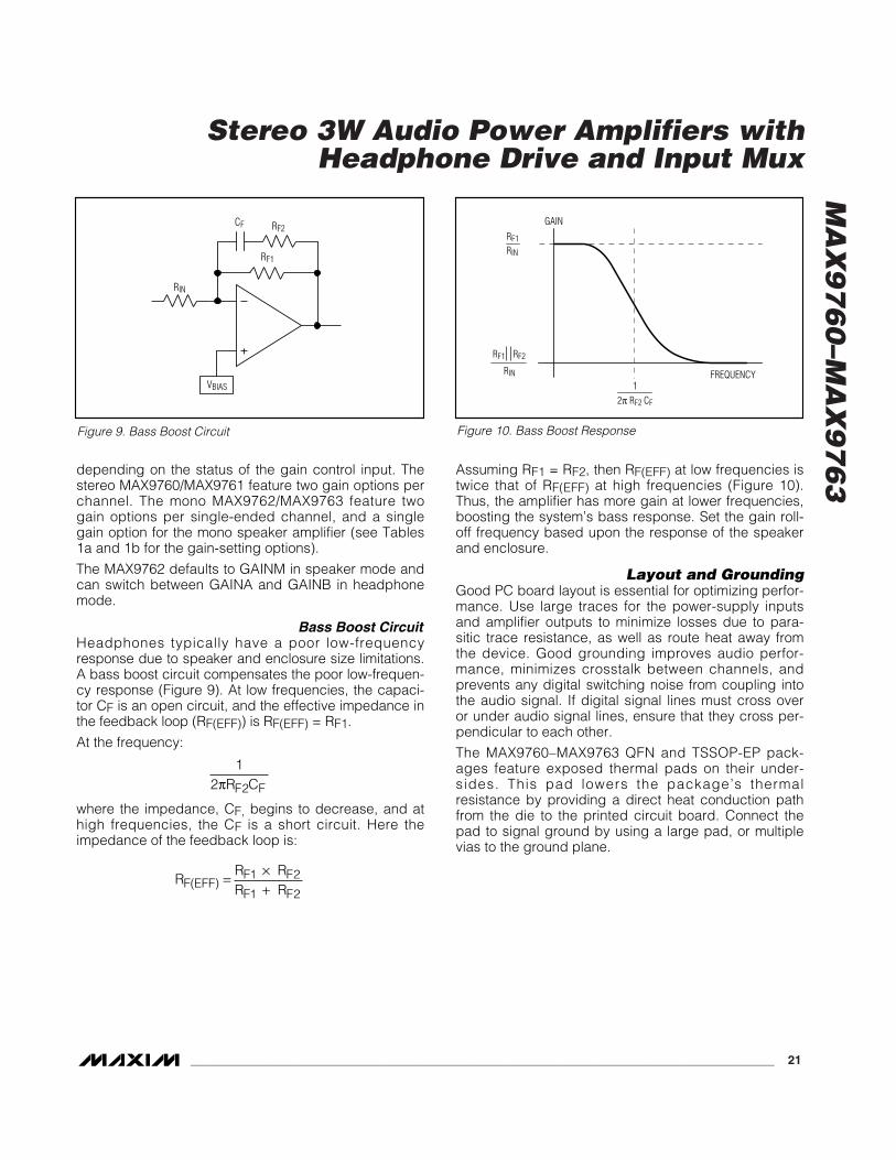
Bass Boost CircuitHeadphones typically have a poor low-frequencyresponse due to speaker and enclosure size limitations.A bass boost circuit compensates the poor low-frequen-cy response (Figure 9). At low frequencies, the capaci-tor CF is an open circuit, and the effective impedance inthe feedback loop (RF(EFF)) is RF(EFF) = RF1.
At the frequency:
where the impedance, CF, begins to decrease, and athigh frequencies, the CF is a short circuit. Here theimpedance of the feedback loop is:
Assuming RF1 = RF2, then RF(EFF) at low frequencies istwice that of RF(EFF) at high frequencies (Figure 10).Thus, the amplifier has more gain at lower frequencies,boosting the system’s bass response. Set the gain roll-off frequency based upon the response of the speakerand enclosure.
Layout and GroundingGood PC board layout is essential for optimizing perfor-mance. Use large traces for the power-supply inputsand amplifier outputs to minimize losses due to para-sitic trace resistance, as well as route heat away fromthe device. Good grounding improves audio perfor-mance, minimizes crosstalk between channels, andprevents any digital switching noise from coupling intothe audio signal. If digital signal lines must cross overor under audio signal lines, ensure that they cross per-pendicular to each other.
The MAX9760–MAX9763 QFN and TSSOP-EP pack-ages feature exposed thermal pads on their under-sides. This pad lowers the package ’s thermalresistance by providing a direct heat conduction pathfrom the die to the printed circuit board. Connect thepad to signal ground by using a large pad, or multiplevias to the ground plane.
R
R RR RF EFF
F F
F F( )
= ×+
1 2
1 2
12 2πR CF F
VBIAS
RIN
RF2
RF1
CF
Figure 9. Bass Boost Circuit
RF1
RF1 RF2
RIN
RIN
2π RF2 CF
1FREQUENCY
GAIN
Figure 10. Bass Boost Response
MA
X9
76
0–M
AX
97
63
Stereo 3W Audio Power Amplifiers withHeadphone Drive and Input Mux
22 ______________________________________________________________________________________
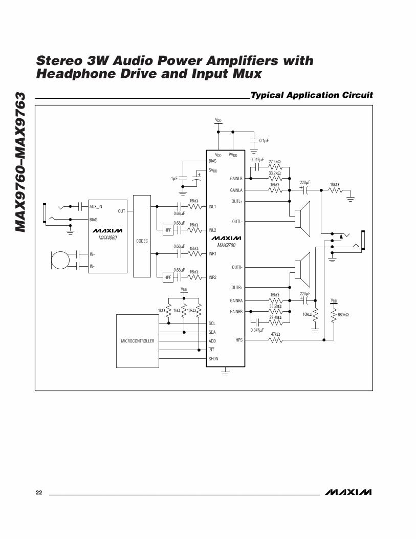
HPF
HPF
MICROCONTROLLER
CODECMAX4060
AUX_IN
BIAS
IN+
IN-
OUT
MAX9760
INR2
INR1
INL2
INL1
SVDD
BIAS
1µF
0.1µF
0.68µF
0.68µF
0.68µF
0.68µF
0.047µF
0.047µF
220µF
220µF
27.4kΩ
27.4kΩ
47kΩ
10kΩ
10kΩ 680kΩ
33.2kΩ
33.2kΩ
15kΩ
15kΩ
15kΩ
15kΩ
15kΩ
10kΩ1kΩ1kΩ
15kΩ
SCL
SDA
ADD
INT
SHDN
GAINLB
GAINLA
OUTL+
OUTL-
OUTR+
GAINRA
GAINRB
OUTR-
HPS
VDD
VDD
VDD
PVDD
VDD
Typical Application Circuit

MA
X9
76
0–M
AX
97
63
Stereo 3W Audio Power Amplifiers withHeadphone Drive and Input Mux
______________________________________________________________________________________ 23
MAX9760
2:1INPUTMUX
INL1
10kΩ
PVDD SVDDVDD
VDD
GAINLB
GAINLA
OUTL+
OUTL-
10kΩ
10kΩ
10kΩ
AUDIOINPUTAUDIOINPUT
INL2
BIASBIAS
GAINSETMUX
2:1INPUTMUX
INR1
10kΩ
GAINRB
GAINRA
OUTR+
OUTR-
10kΩ
10kΩ
10kΩ
AUDIOINPUTAUDIOINPUT
INR2
SCLSDAADDINT
LOGIC
HPSHPS
GND
GAINSETMUX
SHDN
Functional Diagrams

MA
X9
76
0–M
AX
97
63
Stereo 3W Audio Power Amplifiers withHeadphone Drive and Input Mux
24 ______________________________________________________________________________________
MAX9761
2:1INPUTMUX
INL1
10kΩ
PVDD SVDDVDD
GAINLB
GAINLA
OUTL+
OUTL-
10kΩ
10kΩ
10kΩ
INL2
BIASBIAS
GAINSETMUX
2:1INPUTMUX
INR1
10kΩGAINRB
GAINRA
OUTR+
OUTR-
10kΩ
10kΩ
10kΩ
INR2
MUTEHP_ENGAINA/BIN1/IN2
LOGIC
HPSHPS
GND
GAINSETMUX
SHDN
Functional Diagrams (continued)
MA
X9
76
0–M
AX
97
63
Stereo 3W Audio Power Amplifiers withHeadphone Drive and Input Mux
______________________________________________________________________________________ 25
MAX9762
2:1INPUTMUX
INR1
10kΩ
PVDD SVDDVDDGAINRBGAINRA
OUTR+
OUTR-
10kΩ
10kΩ
10kΩ
INR2
BIAS
MIXER
BIAS
GAINSETMUX GAINM
2:1INPUTMUX
INL1
10kΩGAINLB
GAINLA
OUTL10kΩ
INL2
SCLSDAADDINT
LOGIC HPSHPS
GND
GAINSETMUX
SHDN
Functional Diagrams (continued)

MA
X9
76
0–M
AX
97
63
Stereo 3W Audio Power Amplifiers withHeadphone Drive and Input Mux
26 ______________________________________________________________________________________
MAX9763
2:1INPUTMUX
INR1
10kΩ
PVDD SVDDVDDGAINRBGAINRA
OUTR+
OUTR-
10kΩ
10kΩ
10kΩ
INR2
BIAS
MIXER
BIAS
GAINSETMUX GAINM
2:1INPUTMUX
INL1
10kΩGAINLB
GAINLA
OUTL10kΩ
INL2
HP_ENMUTE
GAINA/BIN1/IN2
LOGIC HPSHPS
GND
GAINSETMUX
SHDN
Functional Diagrams (continued)
MA
X9
76
0–M
AX
97
63
Stereo 3W Audio Power Amplifiers withHeadphone Drive and Input Mux
______________________________________________________________________________________ 27
28 27 26 25 24 23 22
8 9 10 11 12 13 14
15
16
17
18
19
20
21
7
6
5
4
3
2
1
MAX9760
THIN QFN
TOP VIEW
INT
SDA
VDD
SVDD
INL1
INL2
GAINLA
SCL
PGND
OUTR
-
PVDD
OUTR
+
PGND
GAIN
RBGAINRA
INR2
INR1
GND
BIAS
HPS
ADD
SHDN
PGND
OUTL
-
PVDD
OUTL
+
PGND
GAIN
LB
28
27
26
25
24
23
22
21
20
19
18
17
16
15
1
2
3
4
5
6
7
8
9
10
11
12
13
14
VDD
INT
SDA
SCL
PGND
OUTR-
GND
PVDD
OUTR+
PGND
GAINRB
GAINRA
INR2
INR1
BIAS
HPS
ADD
SHDN
PGND
OUTL-
PVDD
OUTL+
PGND
GAINLB
GAINLA
INL2
INL1
SVDD
TSSOP
MAX9760
Pin Configurations
28 27 26 25 24 23 22
8 9 10 11 12 13 14
15
16
17
18
19
20
21
7
6
5
4
3
2
1
MAX9761
THIN QFN
TOP VIEW
HPS_EN
MUTE
VDD
SVDD
INL1
INL2
GAINLA
IN1/
2
PGND
OUTR
-
PVDD
OUTR
+
PGND
GAIN
RB
GAINRA
INR2
INR1
GND
BIAS
HPS
GAINA/B
SHDN
PGND
OUTL
-
PVDD
OUTL
+
PGND
GAIN
LB
28
27
26
25
24
23
22
21
20
19
18
17
16
15
1
2
3
4
5
6
7
8
9
10
11
12
13
14
VDD
HPS_EN
MUTE
IN/1V2
PGND
OUTR-
GND
PVDD
OUTR+
PGND
GAINRB
GAINRA
INR2
INR1
BIAS
HPS
GAIN/AVB
SHDN
PGND
OUTL-
PVDD
OUTL+
PGND
GAINLB
GAINLA
INL2
INL1
SVDD
TSSOP
MAX9761
MA
X9
76
0–M
AX
97
63
Stereo 3W Audio Power Amplifiers withHeadphone Drive and Input Mux
28 ______________________________________________________________________________________
28 27 26 25 24 23 22
8 9 10 11 12 13 14
15
16
17
18
19
20
21
7
6
5
4
3
2
1
MAX9762
THIN QFN
TOP VIEW
INT
SDA
VDD
SVDD
INL1
INL2
GAINLA
SCL
PGND
OUTR
-
PVDD
OUTR
+
PGND
GAIN
RBGAINRA
INR2
INR1
GAINM
BIAS
HPS
ADD
SHDNGN
D
N.C.
PVDD
OUTL
+
PGND
GAIN
LB
28
27
26
25
24
23
22
21
20
19
18
17
16
15
1
2
3
4
5
6
7
8
9
10
11
12
13
14
VDD
INT
SDA
SCL
PGND
OUTR-
GAINM
PVDD
OUTR+
PGND
GAINRB
GAINRA
INR2
INR1
BIAS
HPS
ADD
SHDN
GND
N.C.
PVDD
OUTL+
PGND
GAINLB
GAINLA
INL2
INL1
SVDD
TSSOP
MAX9762
Pin Configurations (continued)
28 27 26 25 24 23 22
8 9 10 11 12 13 14
15
16
17
18
19
20
21
7
6
5
4
3
2
1
MAX9763
THIN QFN
TOP VIEW
HPS_EN
MUTE
VDD
SVDD
INL1
INL2
GAINLA
IN1/
2
PGND
OUTR
-
PVDD
OUTR
+
PGND
GAIN
RB
GAINRA
INR2
INR1
GAINM
BIAS
HPS
GAINA/B
SHDNGN
D
N.C.
PVDD
OUTL
+
PGND
GAIN
LB
28
27
26
25
24
23
22
21
20
19
18
17
16
15
1
2
3
4
5
6
7
8
9
10
11
12
13
14
VDD
HPS_EN
MUTE
IN1/2
PGND
OUTR-
GAINM
PVDD
OUTR+
PGND
GAINRB
GAINRA
INR2
INR1
BIAS
HPS
GAINA/B
SHDN
GND
N.C.
PVDD
OUTL+
PGND
GAINLB
GAINLA
INL2
INL1
SVDD
TSSOP
MAX9763
MA
X9
76
0–M
AX
97
63
Stereo 3W Audio Power Amplifiers withHeadphone Drive and Input Mux
______________________________________________________________________________________ 29
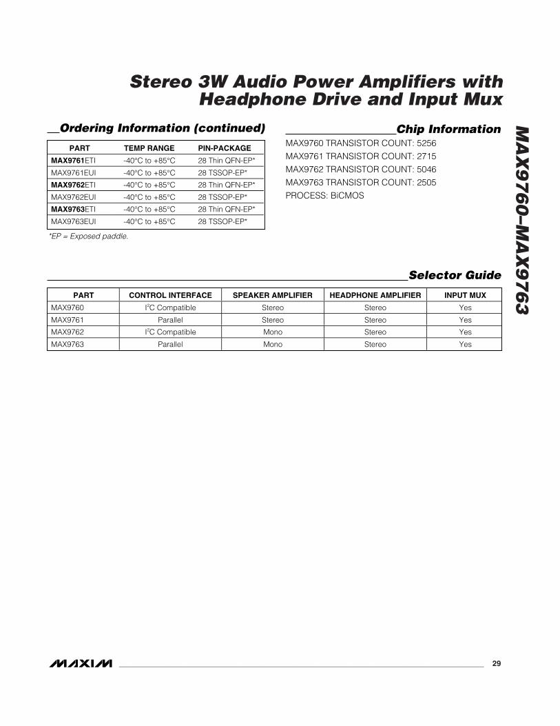
Ordering Information (continued)
PART TEMP RANGE PIN-PACKAGE
MAX9761ETI -40°C to +85°C 28 Thin QFN-EP*
MAX9761EUI -40°C to +85°C 28 TSSOP-EP*
MAX9762ETI -40°C to +85°C 28 Thin QFN-EP*
MAX9762EUI -40°C to +85°C 28 TSSOP-EP*
MAX9763ETI -40°C to +85°C 28 Thin QFN-EP*
MAX9763EUI -40°C to +85°C 28 TSSOP-EP*
Chip InformationMAX9760 TRANSISTOR COUNT: 5256
MAX9761 TRANSISTOR COUNT: 2715
MAX9762 TRANSISTOR COUNT: 5046
MAX9763 TRANSISTOR COUNT: 2505
PROCESS: BiCMOS
Selector Guide
PART CONTROL INTERFACE SPEAKER AMPLIFIER HEADPHONE AMPLIFIER INPUT MUX
MAX9760 I2C Compatible Stereo Stereo Yes
MAX9761 Parallel Stereo Stereo Yes
MAX9762 I2C Compatible Mono Stereo Yes
MAX9763 Parallel Mono Stereo Yes
*EP = Exposed paddle.
MA
X9
76
0–M
AX
97
63
Stereo 3W Audio Power Amplifiers withHeadphone Drive and Input Mux
30 ______________________________________________________________________________________
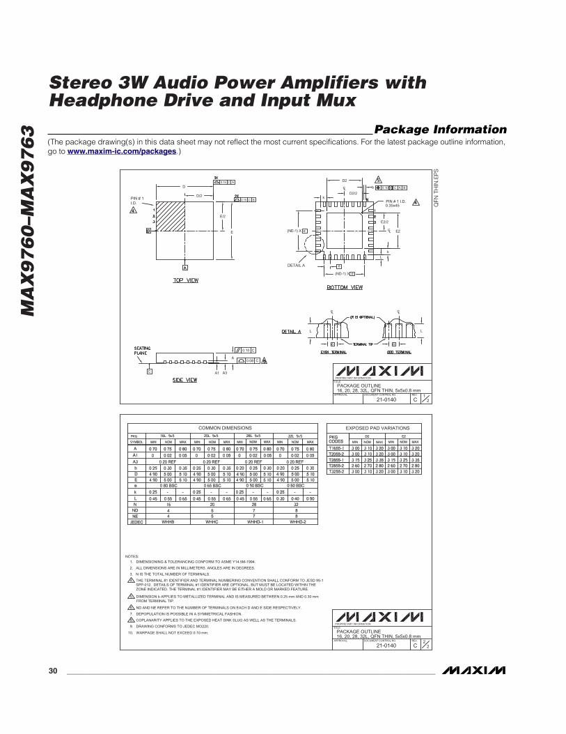
Package Information(The package drawing(s) in this data sheet may not reflect the most current specifications. For the latest package outline information,go to www.maxim-ic.com/packages.)
QFN
TH
IN.E
PS
D2
(ND-1) X e
e
D
C
PIN # 1 I.D.
(NE-1) X e
E/2
E
0.08 C
0.10 C
A
A1 A3
DETAIL A
0.15 C B
0.15 C A
DOCUMENT CONTROL NO.
21-0140
PACKAGE OUTLINE16, 20, 28, 32L, QFN THIN, 5x5x0.8 mm
PROPRIETARY INFORMATION
APPROVAL
TITLE:
CREV.
21
E2/2
E2
0.10 M C A B
PIN # 1 I.D.
b
0.35x45
L
D/2D2/2
LC
LC
e e
LCCL
k
k
LL
22
21-0140REV.DOCUMENT CONTROL NO.APPROVAL
PROPRIETARY INFORMATION
TITLE:
COMMON DIMENSIONS EXPOSED PAD VARIATIONS
1. DIMENSIONING & TOLERANCING CONFORM TO ASME Y14.5M-1994.
2. ALL DIMENSIONS ARE IN MILLIMETERS. ANGLES ARE IN DEGREES.
3. N IS THE TOTAL NUMBER OF TERMINALS.
4. THE TERMINAL #1 IDENTIFIER AND TERMINAL NUMBERING CONVENTION SHALL CONFORM TO JESD 95-1 SPP-012. DETAILS OF TERMINAL #1 IDENTIFIER ARE OPTIONAL, BUT MUST BE LOCATED WITHIN THE ZONE INDICATED. THE TERMINAL #1 IDENTIFIER MAY BE EITHER A MOLD OR MARKED FEATURE.
5. DIMENSION b APPLIES TO METALLIZED TERMINAL AND IS MEASURED BETWEEN 0.25 mm AND 0.30 mm FROM TERMINAL TIP.
6. ND AND NE REFER TO THE NUMBER OF TERMINALS ON EACH D AND E SIDE RESPECTIVELY.
7. DEPOPULATION IS POSSIBLE IN A SYMMETRICAL FASHION.
8. COPLANARITY APPLIES TO THE EXPOSED HEAT SINK SLUG AS WELL AS THE TERMINALS.
9. DRAWING CONFORMS TO JEDEC MO220.
NOTES:
10. WARPAGE SHALL NOT EXCEED 0.10 mm.
C
PACKAGE OUTLINE16, 20, 28, 32L, QFN THIN, 5x5x0.8 mm
MA
X9
76
0–M
AX
97
63
Stereo 3W Audio Power Amplifiers withHeadphone Drive and Input Mux
Maxim cannot assume responsibility for use of any circuitry other than circuitry entirely embodied in a Maxim product. No circuit patent licenses areimplied. Maxim reserves the right to change the circuitry and specifications without notice at any time.
Maxim Integrated Products, 120 San Gabriel Drive, Sunnyvale, CA 94086 408-737-7600 ____________________ 31
© 2003 Maxim Integrated Products Printed USA is a registered trademark of Maxim Integrated Products.
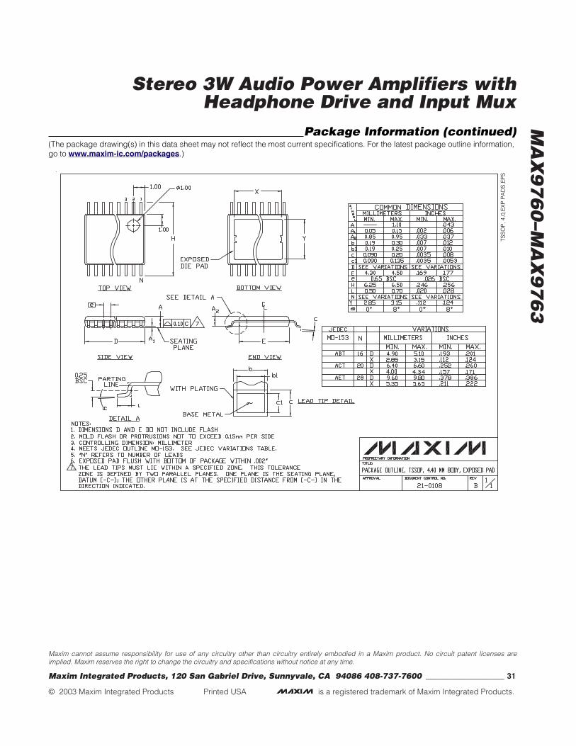
Package Information (continued)(The package drawing(s) in this data sheet may not reflect the most current specifications. For the latest package outline information,go to www.maxim-ic.com/packages.)
TSS
OP
, 4.0
,EX
P P
AD
S.E
PS