
Step 1 : Total EPROM required = 64 KB...
19
1113/Engg/TE/Pre Pap/2013/CMPN/Soln/MP 1 Vidyalankar T.E. Sem. V [CMPN] Microprocessors Prelim Question Paper Solution Step 1 : Total EPROM required = 64 KB Chip size available = 32 KB No.of chips required = 2 No.of sets required = 2 1 2 Set 1 = Ending address = FFFFF H Set size = 32 KB 2 = 64 KB 0FFFF H Starting address = FFFFF 0FFFF = F0000H Even Bank Odd Bank Starting address F0000 H F0001 H Ending address FFFFEH FFFFF H Step 2 : Total SRAM required = 32 KB Chip size available = 16 KB No.of chips required = 2 No.of sets required = 2 1 2 Set 1 : Starting address = 00000 H Set size = 16 KB 2 = 32 KB 07 FFF H Ending address = 00000 H + 07FFF H = 07FFF H Even Bank Odd Bank Starting address 00000 H 00001 H Ending address 07FFEH 07FFF H 1. (a) Vidyalankar
Transcript of Step 1 : Total EPROM required = 64 KB...

1113/Engg/TE/Pre Pap/2013/CMPN/Soln/MP 1
Vidyalankar T.E. Sem. V [CMPN] Microprocessors
Prelim Question Paper Solution
Step 1 : Total EPROM required = 64 KB
Chip size available = 32 KB
No.of chips required = 2
No.of sets required = 2
12
Set 1 = Ending address = FFFFF H Set size = 32 KB 2 = 64 KB
0FFFF H
Starting address = FFFFF 0FFFF = F0000H
Even Bank Odd Bank Starting address F0000 H F0001 H Ending address FFFFEH FFFFF H
Step 2 : Total SRAM required = 32 KB
Chip size available = 16 KB
No.of chips required = 2
No.of sets required = 2
12
Set 1 : Starting address = 00000 H Set size = 16 KB 2 = 32 KB
07 FFF H
Ending address = 00000 H + 07FFF H = 07FFF H
Even Bank Odd Bank Starting address 00000 H 00001 H Ending address 07FFEH 07FFF H
1. (a)
Vidyala
nkar

Vidyalankar : T.E. − MP
1113/Engg/TE/Pre Pap/2013/CMPN/Soln/MP 2
A19
A18
A17
A16
A15
A14
A13
A12
A11
A10
A9
A8
A7
A6
A5
A4
A3
A2
A1
A0
RAM Set1
0y
EB SA = 00000H EA =07FFEH
0 0 0 0 0 0 0 0 0 0 0 0 0 0 0 0 0 0 0
0 0 0 0 0 1 1 1 1 1 1 1 1 1 1 1 1 1 1 0
OB SA = 00001 H EA = 07FFF H
0 0 0 0 0 0 0 0 0 0 0 0 0 0 0 0 0 0 0 0
0 0 0 0 0 1 1 1 1 1 1 1 1 1 1 1 1 1 1 1
EPROM Set1
30 31y . y
EB SA=F0000H EA=FFFFEH
1 1 1 0 0 0 0 0 0 0 0 0 0 0 0 0 0 0 0
1 1 1 1 1 1 1 1 1 1 1 1 1 1 1 1 1 1 1 0
OB SA=F0001H
EA=FFFFF H
1 1 1 1 1 0 0 0 0 0 0 0 0 0 0 0 0 0 0 1
1 1 1 1 1 1 1 1 1 1 1 1 1 1 1 1 1 1 1 1
Step 3 : I/O MAP
Fig. (1) shows the implementation of a 16bit input and 16bit o/p port.
A7 A6 A5 A4 A3 A2 A1 A0
8255 Set 1
EB
PA = 00H 0 0 0 0 0 0 0 0 PB = 02H 0 0 0 0 0 0 1 0 PC = 04H 0 0 0 0 0 1 0 0 CW = 06H 0 0 0 0 0 1 1 0
OB
PA = 01H 0 0 0 0 0 0 0 1 PB = 03H 0 0 0 0 0 0 1 1 PC = 05H 0 0 0 0 0 1 0 1 CW = 07H 0 0 0 0 0 1 1 1
0
1
PA
8255
(Even Bank)
PB
PA 8255 (odd
Bank) PB
16bit input
16bit inputFig. 1
Vidyala
nkar

Prelim Question Paper Solution
1113/Engg/TE/Pre Pap/2013/CMPN/Soln/MP 3
Addressing modes of 8085 There are 5 addressing modes available in 8085 to address the data (operand). i) Immediate addressing mode : In this mode, the data is a part of the instruction itself. e.g. MVI A, 30 H.
In the above example, the data i.e., 30 H which is to be moved into accumulator is specified as a part of the instruction, hence it is immediate addressing.
ACC
X X (Before execution)
MVI A, 30 H
ACC
30 H (After execution) ii) Register addressing mode : In this mode, the register that contains the operand is specified
as a part of the instruction. e.g. MOV A, B
2. (a)
Vidyala
nkar

Vidyalankar : T.E. − MP
1113/Engg/TE/Pre Pap/2013/CMPN/Soln/MP 4
ACC B
XX 30 H (Before execution)
MOV A, B ACC B
30 H 30 H (After execution)
In the above example, the data (i.e. 30 H) to be moved into accumulator is available in B register and the instruction specifies that the contents of B register is to be moved to accumulator. Hence it is register addressing mode.
iii) Direct addressing mode : In this mode, the address of memory location that contains the
operand is specified as a part of the instruction. e.g.
ACC memory XX 2050 H 30 H (Before execution)
LDA 2050 H
ACC 30 H 2050 H 30 H (After execution)
In the above example, the address of memory location (i.e., 2050 H) which contains the operand 30H to be loaded in accumulator is specified in the instruction hence it is direct addressing mode.
iv) Indirect addressing mode : In this mode, the register pair that contains the address of memory location which contains the operand is specified in the instruction.
e.g. ACC B C memory
XX 2050 H 2050 H 30 H (Before execution)
LDAX B ACC B C memory
30H 2050 H 2050 H 30 H (After execution)
In this above example, the register pair B (i.e., BC) that contains the address 2050H of a memory location which has the operand 30 H is specified in the instruction.
Hence, the above instruction is of the type indirect addressing mode. v) Implicit/Implied addressing mode : In this addressing mode, no specification about the
operand is specified in the instruction, since the microprocessor knows the operand internally as it is fixed. e.g. RAL This instruction means rotate left the contents of accumulator through carry by 1 bit. In this instruction the accumulator that contains the operand is not specified in the instruction, rather the microprocessor is aware about the operand as this instruction only operates on accumulator, hence this instruction is implied or implicit addressing mode.
Vidyala
nkar

Prelim Question Paper Solution
1113/Engg/TE/Pre Pap/2013/CMPN/Soln/MP 5
8086 Architecture Block Diagram :
8086 is a 2 stage p divided into Bus interface unit and Execution Unit.
Bus Interface Unit It performs the following operations. i) It responds to the execution units demand to fetch instructions or data which has higher
priority. ii) It generates 20–bit physical address for memory. iii) It executes Bus cycles. iv) It accesses external memory and I/O modules. v) It fetches opcode into instruction byte queue or data through its 16 bit data bus. EU demands for instruction bytes which are provided from the 6–byte queue of the BIU. The BIU fetches 2 or more bytes ahead of time to fill the queue. If the queue is full and there is no demand from EU side, BIU executes idle cycles.
If the EU demands in between the bus cycle, BIU completes the current bus cycle and then responds to the EU’s demands. Fetching instruction bytes ahead of time is called Pipelining.
2. (b)
Vidyala
nkar

Vidyalankar : T.E. − MP
1113/Engg/TE/Pre Pap/2013/CMPN/Soln/MP 6
BIU contains Segment Registers, Instruction pointer, Address Conversion Mechanism & 6–byte pre–fetched queue.
Segment Registers 8086 provides four 16–bit segment register. (1) Code Segment Register (2) Data Segment Register (3) Stack Segment Register (4) Extra Segment Register
1) Code Segment Register (CS) : It holds the segment address or base address of a program memory. Contents of this register can only be modified through branch instructions.
2) Data Segment Register (DS) : It holds the upper (higher) 16–bits of the base address of data memory.
3) Stack Segment Register (SS) : It holds the higher 16–bits of the base address of stack memory.
4) Extra Segment (ES) : It holds the higher 16–bits of the base address of extra memory which is used to support the data memory.
Instruction Pointer (IP) : It is a 16–bit register that hold the offset address of program memory. It is used with CS to fetch instruction bytes. The contents of IP can also be modified by only branch instructions.
Address Conversion Mechanism : It is a part of Bus Interface Control block. It generates 20–bit physical address of memory by using 16–bit segment address and 16–bit offset address.
The 20–bit address generated is placed on the address bus. It shifts the segment address left by 4–bits and adds zeros on the lower nibble position. It then adds the offset address to the shifted contents to generate the actual 20–bit physical address. 16–bit segment address is provided by CS, DS, SS or ES. 16–bit offset is provided by IP or EU.
Instruction Byte Queue : It is a 6–byte (FIFO) queue. The BIU fetches the contents of program (CS) memory into this queue. It does not fetch the contents of data memory, stack memory or extra memory. It executes instruction fetch cycles until the queue is full. When JMP or CALL instruction is executed which transfers the control of program the next sequential instruction, now the instructions are not required. Therefore the queue is dumped (Cleared) and is filled from the contents of JUMP location/CALL location in CS memory. Execution Unit : It performs the following operations – 1. It takes instruction byte from the queue and loads Opcode bytes into Instruction Register and
operand bytes into General Purpose Register or Special Purpose Register. 2. It decode the instructions. 3. It performs arithmetic, logic, data transfer & decision making operations. 4. It sends request Signal to BIU to access the external memory input/output module. 5. It operates with respect to T – states. It contains four 16–bit General Purpose Register, four
16bit Special Purpose Registers, ALU, flag resister, Operand register, Instruction register, Instruction decoder and Timing and Control unit.
General Purpose Registers 8086 provides only four 16–bit general purpose register. They are AX, BX, CX, DX. Each of these registers can be used as two 8–bit register (AH, AL, BH, BL, CH, CL, DH & DL)
AX : AX is always used to hold I/O data. It is used to hold operands and results during execution of multiplication and division instruction. It functions as Accumulator in string operations. BX : In base relative addressing mode it holds the offset address of data memory. CX : It indicates length of string in string operations. It holds count value during the execution of loop instruction. It indicates no. of times the contents of accumulator is to be shifted or rotated to right or left.
DX : It is used with AX to hold the result of multiplication and division. It is used to hold the address of I/O port in Indirect I/O addressing mode.
Vidyala
nkar

Prelim Question Paper Solution
1113/Engg/TE/Pre Pap/2013/CMPN/Soln/MP 7
Special Purpose Registers 8086 provides four 16–bit special purpose registers viz. (1) Stack Pointer (2) Base Pointer (3) Source Index (4) Destination Index.
Stack Pointer Register (SP) : It is used with SS to access stack memory which operates in LIFO mode SP is always used by PUSH, POP, CALL and RETURN instruction.
Base Pointer (BP) : It is used to hold offset of stack memory in Random Access Mode. It is used with SS so that any Intermediate Location in the stack can be accessed directly. It can be used with CS, DS or SS with Segment over ride prefix.
Source Index (SI) : It is used to hold offset address of data memory in normal operation. And offset address of source block in data segment for string operation. Used with CS, SS, ES registers.
Destination Index (DI) : It is used to hold offset address of data memory in normal operation and offset address of destination block in extra segment for string operation. Only used with ES register.
Arithmetic & Logic Unit : It performs 8 bit/16 bit addition, subtraction logical and ‘And’, ‘or’ ‘Ex–or’ and complement operation.
Instruction Register : It is an 8 bit register which fetches the Opcode byte from queue.
Instruction Decoder : Decodes the contents of instruction register and sends decoded information to Timing and Control circuitry.
Timing and Control Circuit : It operates with respect to clock and synchronizes the operation of different modules on the chip. i) 8086 uses 16 bit base address & 16 bit effective address to from the physical address of the
desired location e.g. If CS = 4000H
IP = 1250H Logical address physical address = (4000)16 (16)16 + (1250)16
= (40000)16 + (1250)16 = (41250)16
Thus physical address of 8086 is 20 bit wide. So it can access 1 MB memory (220 8 = 1MB) = 24 216 8 = 16 64 KB) This 1 MB memory is divided into 16 memory segment each of 64 KB
ii) 8086 can access at a time only four memory segments. They are CS, DS, SS, Es memory. Functions: CS memory: To store instruction fetch operands. DS memory: To store data. SS memory: To perform stack operations. ES memory: To perform string operations. Selection of above memories is done with the help of 4 segment registers which store the base address. These are CS – code segment, DS – data segment, SS – stack segment, ES – extra segment. Physical address is the actual address used by the microprocessor to address any location. It is formed by combining one or more logical addresses in a proper way. Logical addresses give part of actual address of the memory location. They are limited by size of internal registers.
e.g. If CS = 4000H IP = 1250H
Logical address
physical address = (4000)16 (16)16 + (1250)16 = (40000)16 + (1250)16
= (41250)16. This is actual address of the location.
Advantages i) It permits programmer to access 1 MB memory even through address associated with the
instruction is 16 bit.
3. (a)
Vidyala
nkar

Vidyalankar : T.E. − MP
1113/Engg/TE/Pre Pap/2013/CMPN/Soln/MP 8
ii) Instruction, data, stack of a program can be more than 64KB memory. iii) It permits separate memory area for instruction, data or stack. so one program can work on
different sets of data. iv) This method is very useful in multiprogramming. Disadvantages : Even though the memory capacity is 16 64KB, microprocessor can access at a time only 4 64KB memory. MOV AX, 0000H MOV DS, AX ; Initialize DS MOV ES, AX ; Initialize ES MOV SI, 0200H ; Initialize SI MOV DI, 0300H ; Initialize DI MOV CX, 000CH ; Initialize counter = Length of string CLD ; clear direction flag BACK :MOVSB ; move string byte from source to destination
DEC DI DEC DI DEC CX JNZ BACK INT A5 ; Halt
There are 2 formats for CWR which is descriminated by bit D7 of CWR. (i) CWR format for BSR mode (when bit D7 = 0).
0 0 0 PC0
0 0 1 PC1 0 1 0 PC2 0 1 1 PC3 1 0 0 PC4 1 0 1 PC5 1 1 0 PC6 1 1 1 PC7
This mode is available to Port C only. Individual bits of Port C can be set on reset by writing appropriate command in CWR. D3, D2 and D1 bits position of the command identifies the Port C bit which is to be affected and the D0 bit of command specifies whether to set or reset the bit selected by D3, D2 & D1.
3. (b)
4. (a)
0 X X X
D7 D6 D5 D4 D3 D2 D1 D0
BSR mode Port C bit 0 Reset 1 Set
Select the Port C bitD3 D2 D1
Not usedgenerally set to 0
Vidyala
nkar

Prelim Question Paper Solution
1113/Engg/TE/Pre Pap/2013/CMPN/Soln/MP 9
(ii) CWR format for I/O mode (D7 = 1). (i) Mode 0 :
D7 D6 D5 D4 D3 D2 D1 D0
1
Port C lower (PCo PC3) 0 output 1 input
Port B (PBo PB7) 0 output 1 input
Mode of Port B 0 mode 0 1 mode 1
Port C upper (PC4 PC7)0 output 1 input
Port A (PA0 PA7) 0 output 1 input
Mode for Port A 00 mode 0 01 mode 1 1X mode 2
I/O mode
4. (b)
CLK
WR n = 4
1
GATE 0
01234OUT
4 3 3 3 2 1 0
1
GATE 0
n = 4 n = 5 WR
4 3 2 5 4 3 2 1 0
1
GATE 0
OUT
OUT
Vidyala
nkar

Vidyalankar : T.E. − MP
1113/Engg/TE/Pre Pap/2013/CMPN/Soln/MP 10
1) After control word is written in CWR GATE pin is held low. 2) Once the count is loaded into the selected counter, counting starts and OUT pin is made low if it is
not low. 3) When Terminal count is reached OUT pin goes high and remains high until count is reloaded.
(Case 1) 4) This high status of OUT pin can be used to interrupt p on trap, RST 7.5, RST 6.5 & 5.5 or IR pin
of 8259. 5) If GATE goes low while counting then counter stops counting till GATE goes high again
(Case 2). 6) If counter is loaded with new count values, when counting was in progress then current
count is lost and counter starts with new count (Case 3).
(ii) Mode 1 : 8254 as 1 Shot/Monostable 1) After control word is written, the out pin is held in high state. 2) After loading the counter, counting does not start (until a trigger appears on GATE input). 3) Counting starts after trigger is applied at GATE input (i.e. rising edge arrives at GATE
input) and OUT pin goes low. 4) OUT pin goes high on Terminal count (Case 1). 5) If GATE goes low counting is not affected. 6) If GATE goes low to high i.e. new rising edge arrives when counting is in progress then
some original count gets reloaded and counter starts counting again. (Case 2) 7) If new count is loaded then present count is not affected and hence duration of pulse will not be
affected. 8) OUT pin can be used to interrupt p in TRAP, RST 7.5, 6.5 and 5.5 or IR pin of 8259.
Then counter of 8254 can work as programmable monostable multivibrator where pulse duration can be changed by writing new count values.
(iii) Mode 3 : Square Wave generator
1) OUT pin remains high for half of the count and low for remaining half of the count; if even count is loaded.
2) If ODD count is loaded, then OUT pin remains high for 2
1n counts and low for 2
1n
counts where n is the value of count loaded. 3) For even count, count decrements by 2 on falling edge of every clock pulses (Case 1). 4) For ODD count on first clock pulse count decrements by 1 and on subsequent clock
pulses count decrements by 2. After Terminal count, OUT pin goes low and on first clock pulse count decrements by 3
and on subsequent clock pulses count decrements by 2. (Case 2)
CLK
WR n = 3
1
0 GATE
0123OUT
3 2 1 2 1 0
1
0 GATE
OUT 3
CASE 1 :
CASE 2 :
Vidyala
nkar

Prelim Question Paper Solution
1113/Engg/TE/Pre Pap/2013/CMPN/Soln/MP 11
5) On reaching Terminal count pin changes the state, counter is reloaded and process repeats. 6) High level at gate is must for counting. Low level at GATE disables counting and forces
OUT pin high. Rising edge at GATE reloads the counter and counting starts. 7) If reloaded with new values, then present period is not affected new value is consider
only after present count gets over. It gives continuous waveform being a generator 8) Thus counter of 8254 can work as a square wave generator where period can be
controlled by changing the value of count.
(iv) Mode 5 : Hardware Triggered Stroke
1) Out pin is initially high after control word is written. 2) Counting does not start after initializing or loading the counter even if GATE is high. 3) Counting starts when trigger is applied at GATE i.e. rising edge must arrive at GATE. 4) OUT pin goes low only for one clock cycle after Terminal count is reached (Case 1) 5) If GATE goes low the OUT pin is forced high and counting stops. Counting begins from
start when rising edge arrives at GATE (Case 2). 6) If new count is loaded, then old count is lost ((if counting was going on) and counter starts from
new count). 7) Counter does not give continuous waveforms because it is not a generator.
CLK
WRn = 4
CASE 1: 1
0 GATE
OUT
4 3 2 1 0
CASE 2: 1
0 GATE
OUT
43 2 1 0 334 3
CLK
WR
Case 1 : 1
0
n
even count
n = 6 LASTCOUNT
OUT Case 2 : odd count
OUT
n = 7 LASTCOUNT
6 4 2 0/6 4 2 0/6 4 2 0/6
n/2 C.C n/2 C.C4 2 0/7 4 2 0/7 4 2 0/767
2
1n C.C 2
1n C.C
GATE
6
Vidyala
nkar

Vidyalankar : T.E. − MP
1113/Engg/TE/Pre Pap/2013/CMPN/Soln/MP 12
The 8259 can 1. Manage 8 interrupts 2. Vector the interrupt request anywhere in the memory map. 3. Resolves eight levels of interrupt priorities in a variety of modes 4. Mask each interrupt request individually. 5. Read the status of pending interrupts, in service interrupts and masked interrupts 6. Be set up to accept either level triggered ( ) or edge triggered ( )interrupt request 7. Can be expanded to 64 priority levels by cascading additional 8259s 8. Can be set up to work with either the 8085 p mode/8086/8088 p mode
1. Fully Nested Mode : It is a general purpose mode. IR0 highest priority IR1 lowest priority
Any IR can be assigned to highest priority In that case priority sequence will begin at that IR. e.g. IR4 has highest priority then
IR0 IR1 IR2 IR3 IR4 IR5 IR6 IR7 4 5 6 7 0 1 2 3
7 lowest priority 0 Highest priority
2. Automatic Rotation Mode : In this mode, device after being serviced, receives the lowest priority. e.g. IR4 is just being serviced
IR0 IR1 IR2 IR3 IR4 IR5 IR6 IR7 3 4 5 6 7 0 1 2
3. Specific Rotation Mode : This mode is similar to Automatic Rotation Mode except that the user can select any IR for the lowest priority, thus fixing all other priorities
INTERRUPT VECTOR TABLE (IVT): In 8086, the first 1KB memory from 00000 to 003FF is used for IVT. This table stores the values of IP & CS of each ISR & so physical address of that ISR can be calculated.
To store physical address of each ISR we need 4 memory locations therefore this table can give physical addresses of 256 ISRs (i.e. 256 4 = 1024 ≈ 1K). These ISRs are known as Type 0, Type1, …., Type 255.
Interrupt Sequence: Whenever microprocessor is interrupted the following
action takes place. It is known as Interrupt sequence.
For Eg: Consider Type 35 ISR ,
The following action takes place 1) PUSH contents of Flag Register, CS, IP (i.e.
FCI) into the stack memory pointed by SP. Now, SP is decremented by 6.
2) Trap flag (TF) is stored temporarily i.e. TEMP = TF. 3) TF & IF are cleared i.e. TF = 0 & IF = 0. 4) Physical address of IVT is calculated as
follows PA = 4 35 = (140)10 = (8C)16 = (0008C)16. The contents of 0008C, 0008D is placed in IP, then contents of 0008E, 0008F is placed in CS. Now, physical address of ISR is calculated by using contents of CS & IP.
5) Microprocessor begins to execute ISR.
5. (a)
5. (b)
5. (c)
CSH
CSL
IPH
IPL
CSH
CSL
IPH
IPL CSH
CSL
IPH
IPL
Vidyala
nkar

Prelim Question Paper Solution
1113/Engg/TE/Pre Pap/2013/CMPN/Soln/MP 13
6) At the end of ISR, the instruction IRET is executed. Now, microprocessor comes back to main program by poping the contents of memory pointed by SP into IP, CS, FR (flag register). Now, SP is incremented by 6.
7) Microprocessor continues the main program. Dedicated (Or Predefined) Interrupts: Type 0 to Type 4 are known as dedicated interrupts.
The reason is these ISRs always perform a particular task. Type 0: Divide by Zero Microprocessor performs Type 0 ISR if after division it is not able to store the result in the
destination register. By using this ISR, error can be eliminated.
Type 1: Single Step After executing every instruction, microprocessor checks Trap flag TF. If TF = 1, microprocessor executes Type 1 ISR & then comes back to main program. Here it
executes next instruction & then again executes Type 1 ISR. This action continues till TF is cleared. This ISR is used to debug the main program. But this method is time consuming.
Type 2: NMI Whenever request is present in NMI, then microprocessor executes Type 2 ISR. This ISR is used
to answer the request in NMI.
Type 3: Breakpoint Whenever microprocessor executes INT instruction, then microprocessor executes Type 3 ISR.
this ISR is used for debugging when single stepping is more time consuming i.e. Programmer uses INT instruction after a group of instruction in the main program.
Type 4: Overflow Whenever microprocessor executes the INTO instruction it checks overflow flag. If OF is reset,
control continues sequentially. If OF is set microprocessor executes Type 4 ISR . This ISR is used to eliminate the error taken place in signed arithmetic.
Type 5 to 31 : Reserved.
Type 32 to 255 : These are non maskable user defined interrupt types.
Interrupt
MAIN PRG
PUSH FLAGClear IE & TF
PUSH CS PUSH IP
Get new CS &IP from IVTusing ponter toIVT (T
POP IP POP CS
POP Flag
ISR
IRET
New CS IP
Vidyala
nkar
Vidyalankar : T.E. − MP
1113/Engg/TE/Pre Pap/2013/CMPN/Soln/MP 14
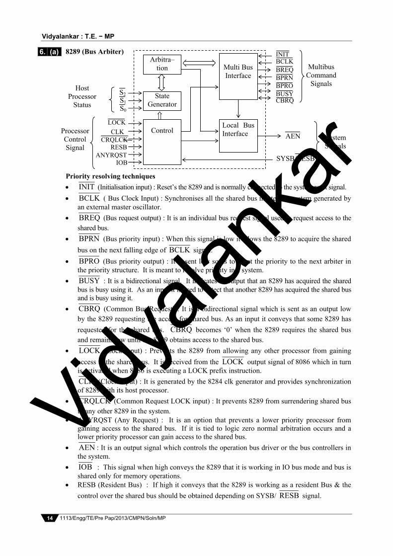
8289 (Bus Arbiter)
Priority resolving techniques
INIT (Initialisation input) : Reset’s the 8289 and is normally connected to the system reset signal.
BCLK ( Bus Clock Input) : Synchronises all the shared bus masters in system generated by an external master oscillator.
BREQ (Bus request output) : It is an individual bus request signal used to request access to the shared bus.
BPRN (Bus priority input) : When this signal is low it allows the 8289 to acquire the shared
bus on the next falling edge of BCLK signal.
BPRO (Bus priority output) : It is sent low so as to grant the priority to the next arbiter in the priority structure. It is meant to resolve priority in a system.
BUSY : It is a bidirectional signal. It indicates as output that an 8289 has acquired the shared bus is busy using it. As an input it is used to detect that another 8289 has acquired the shared bus and is busy using it.
CBRQ (Common Bus Request) : It is a bidirectional signal which is sent as an output low by the 8289 requesting the access for shared bus. As an input it conveys that some 8289 has
requested for the shared bus. CBRQ becomes ‘0’ when the 8289 requires the shared bus and remains low until the 8289 obtains access to the shared bus.
LOCK (Lock input) : Prevents the 8289 from allowing any other processor from gaining
access to the shared bus. It is received from the LOCK output signal of 8086 which in turn is activated when 8086 is executing a LOCK prefix instruction.
CLK (Clock input) : It is generated by the 8284 clk generator and provides synchronization of 8289 with its host processor.
CRQLCK (Common Request LOCK input) : It prevents 8289 from surrendering shared bus to any other 8289 in the system.
ANYRQST (Any Request) : It is an option that prevents a lower priority processor from gaining access to the shared bus. If it is tied to logic zero normal arbitration occurs and a lower priority processor can gain access to the shared bus.
AEN : It is an output signal which controls the operation bus driver or the bus controllers in the system.
: This signal when high conveys the 8289 that it is working in IO bus mode and bus is shared only for memory operations.
RESB (Resident Bus) : If high it conveys that the 8289 is working as a resident Bus & the
control over the shared bus should be obtained depending on SYSB/ RESB signal.
6. (a) Arbitra–
tion
State Generator
Control Local BusInterface
Multi Bus Interface
S2
S1
S0
LOCK
CLK CRQLCK
RESB ANYRQST
IOB
INIT BCLK BREQ BPRN BPRO BUSY CBRQ
AEN
SYSB/RESB
Multibus Command
Signals
System Signals
Processor Control Signal
Host Processor
Status
Vidyala
nkar

Prelim Question Paper Solution
1113/Engg/TE/Pre Pap/2013/CMPN/Soln/MP 15
8 2 5 0
8086
DTE
Fig. 1
SYSB/ RESB (System Bus/Resident Bus) : This signal is considered only in resident bus mode(i.e. when RESB is high). If this signal is high it means that 8289 must request for access to shared system bus. If ‘0’ it means that the host processor is accessing its local resident bus and hence the shared bus is not requested.
Closely coupled configuration Loosely coupled configuration 1] In this 8086 & other processor share
memory, I/O bus control logic and clock generator. Here 8086 is the master or host and supporting processor is slave. Therefore, bus request signal from supporting processor has to be connected to master.
1] This configuration consists of many modules, each module may consist of a) only 8086 or b) 8086 with 8087 or c) 8086 with 8089 or d) 8086 with 8087 & 8089 etc
2] Bus access control logic is provided by the master
2] Many modules share system memory & system IO through system bus. therefore, there must be system bus control logic to resolve bus contention problem. For local memory & IO of each module, local buses are used with local bus control logic
3] This configuration is used for small systems
3] They are used for medium size to large size system.
4] They are of 3 types a) 8086 with co-processor 8087 b) 8086 with IO-processor 8089 c) 8086 with co-processor & IO processor
(8087 & 8089)
4] Usually features a) Individual resident bus & a common
system bus b) Local IO bus & common system bus
5] No problem of bus congestion 5] As the number of modules go on increasing, problem of bus congestion takes place.
6] It can be implemented only in above 3 types
6] More modules can be added very easily
EIARS-232C Serial Interface Standard The Electronics Industries Association( EIA) developed a EIA standard RS 232C for handshaking between DTE & DCE.
i) This standard specifies the function of 25 signals for serial data transfer. The important
signals are TXD, RXD, RTS,CTS,DSR,DTR etc. ii) It also specifies the voltage levels, impedance levels, rise time, fall time, max. bit rate for these
signal lines.
6. (b)
7. (a)
Vidyala
nkar

Vidyalankar : T.E. − MP
1113/Engg/TE/Pre Pap/2013/CMPN/Soln/MP 16
e.g. Logic 1 3 to –15 V Logic 0 +3 to +15 V. iii) To make RS 232C logic compatible with TTL ( 0 to 5V) we use RS 232C line driver MC
1488 ( to convert TTL into RS 232C logic) & RS 232C line receiver MC 1489 ( to convert RS 232C logic into TTL logic)
iv) To interface RS 232C 25 signals pin connectors DB – 25P & DB – 25S are used. Figure 1 shows interfacing of 2 DTEs for proper interfacing. We need cross over connection for this purpose an adapter is used as shown in figure 1. This cross over connection is called Null Modem.
Figure 2 shows interfacing of DTE with DCE (modem) for long distance communication through telephone line.
There are 5 interrupt lines available. Interrupt line and their characteristics are as follows :
Interrupt line Priority Triggering Maskable/
Nonmask ISR
address
(RST 4.5) TRAP
1 (highest)
Non mask 0024H
Vectored interrupts
RST 7.5 2 maskable 003CH
RST 6.5 3 maskable 0034H
RST 5.5 4 maskable 002CH
INTR 5
(Lowest) maskable No fixed address
Nonvectored interrupts
7. (b)
+ve level and edge
+ve edge +ve level
MO
DE
M (
DC
E)
Fig. 2
Vidyala
nkar

Prelim Question Paper Solution
1113/Engg/TE/Pre Pap/2013/CMPN/Soln/MP 17
Since the ISR address for INTR line is not fixed, microprocessor generates in response an INTA signal. This signal is generated for INTR only and is used to get the information about the ISR address from interrupting device.
Flag Register:
D15 D14 D13 D12 D11 D10 D9 D8 D7 D6 D5 D4 D3 D2 D1 D0
X X X X OF DF IF TF SF ZF X AF X PF X CF
D9 : TF : Trap Flag (Single step) D10 : IF : Interrupt Enable Flag / Interrupt Flag D11 : DF : Direction Flag D12 : OF : Overflow Flag
8086 has following two types of flags:
1) Conditional flags a) Carry flag: This flag is set whenever there is overflow from MSB after performing arithmetic
operation, otherwise it is reset (for 8 bit operation, overflow is from B7 bit, for 16 bit operation, overflow is from B15 bit.
b) Parity flag: This flag is set if lower order 8 bit of the result consists of even no. of 1’s, otherwise it is reset
c) Auxiliary carry flag: This flag is set whenever there is overflow from lower order 4 bits after performing arithmetic operation, otherwise it is reset
d) Zero flag: This flag is set whenever the result is zero after performing ALU operation, otherwise it is reset
e) Sign flag: This flag is set if MSB of the result is equal to 1 after performing ALU operation, otherwise it is reset (for 8 bit data it is set when B7 = 1, for 16 bit data it is set when B15 = 1).
f) Overflow flag: This flag is set if result cannot be stored in destination location, otherwise it is reset. This flag is checked during signed arithmetic operation. It can be checked using an instruction INTO.
It will set when i) Overflow from B6 to B7 (or from B14 to B15) & ii) No overflow from B7 (or from B15).
2) Control flags a) Trap flag: When this flag is set, 8086 enters into single stepping mode. In this mode,
system will execute one instruction and wait for further direction from the programmer. It is used to debug the program. If it is reset, control continues sequentially.
b) Interrupt enable flag: When it is set, 8086 recognizes interrupt INTR. If it is reset, it will not recognize interrupt INTR i.e. INTR is maskable interrupt
c) Direction flag: When it is set, content of SI & DI automatically decremented ( by 1 or 2) after executing the string instruction. If it is reset, content of SI & DI are automatically incremented (by 1 or 2) after executing the string instruction.
Operand Register : It is not available to the user and is used by the control section to hold the operands and result temporarily.
(i) PUSH : PUSH SOURCE
The PUSH instruction decrements the stack pointer by 2 and copies a word from a specified source to the location in the stack segment where SP then points. The source of the word can be General purpose register and a segment register or memory. No flags are affected by this instruction.
e.g: PUSH BX : decrement SP by 2, copy BX to stack. PUSH DX : decrement SP by 2, copy DS to stack.
7. (c)
8085 Flags Control Flags
7. (d) Vidyala
nkar

Vidyalankar : T.E. − MP
1113/Engg/TE/Pre Pap/2013/CMPN/Soln/MP 18
(ii) POP : POP destination The POP instruction copies a word from the stack location pointed to by the stack pointer to a destination specified in the instruction. The destination can be general purpose register, a segment register or a memory location. The data in the stack is not changed. After the word is copied to the specified destination, the stack pointer is automatically incremented by 2 to point to the next word on the stack. No flags are affected by the POP instruction.
e.g: POP DX ; copy a word from top of stack to DX ; increment SP by 2. POP DS ; copy a word from top of stack to ; DS increment SP by 2. (iii) XLAT: transfer a byte in AL
The contents of the memory location having effective address formed by adding contents of BX & contents of AL is moved into AL.
The base address will be in DS. Let [AL] = 04H, [BX] = 1234H, EA = 1234 + 04 = 1238H. Let DS = 5000H
(iv) IMUL: This instruction multiplies a signed byte from some source times a signed byte in AL
or a signed word from some source times a signed word in AX. When a byte from some source is multiplied by AL, the signed result will be put in AX. When a word from some source is multiplied by AX, the result can be as large as 32 bits. The high order word of the signed result is put in DX and the low order word of the signed result is put in AX. If the magnitude of the product does not require all the bits of destination, the unused bits will be filled with copies of the sign bit. If the upper byte of a 16 bit result or the upper word of 32 bit result contain only copies of the sign bit then CF & OF will both be zero. If the upper byte of 16 bit result or the upper word of 32 bit result contains part of product CF & OF will both be 1.
Examples : 1) 69 14 AL = 0100 0101 = (69) 10 BL = 0000 1110 = (14) 10 IMUL BL AX = 03C6H = (966) 10 MSB = 0, positive result, magnitude in true form SF = 0, CF, OF = 1 2) 28 59 AL = 1110 0100 = -(28)10 BL = 0011 1011 = +(59)10
IMUL BL AX = F98CH = (1652)10 MSB = 1, negative result magnitude in 2’s complement event. SF, CF, OF = 1.
Vidyala
nkar

Prelim Question Paper Solution
1113/Engg/TE/Pre Pap/2013/CMPN/Soln/MP 19
(v) DAA ( Decimal Adjust for Addition): The DAA instruction follows the ADD instruction to adjust the result into a BCD result. It works only on AL
Example :
Mixed mode programming with C-Lang and Assembly ‘C’ provides extremely fast and compact object code, but it is not as fast and compact as object code generated by an excellent programmer using assembler. It is true that time needed to write program in an assembly language is more than using higher level language. However, there are special cases where a specific function is coded in assembly language to decrease its execution time. For example : A floating point math package might be coded in assembler because it is used frequently and has great effect on the execution speed of a program that uses it. There are also situations in which special hardware devices need exact timing and it is must to write program in assembly language to meet this strict timing requirement. Certain instructions can not be executed by a ‘C’ program. For Example : There is no built in bit wise rotate operation in ‘C’. To efficiently perform this it is necessary to use assembly language routine. Though ‘C’ is Efficient and Powerful, we some times require to write a routine using assembly language to : i) Increase speed and efficiency of the routine. ii) Perform some machine specific function unavailable in Microsoft C and turbo C. iii) Use third party routines.
7. (e)
Vidyala
nkar


![B.E. Sem. VII [INFT] Vidyalankarvidyalankar.org/file/engg_degree/prelim_paper_soln/SemVII/INFT/DWM.… · Therefore it flows into a Decision Support System (DSS) or into marketing](https://static.fdocuments.net/doc/165x107/5a9db36e7f8b9a85318b9f3f/be-sem-vii-inft-vi-therefore-it-flows-into-a-decision-support-system-dss.jpg)
![S.E. Sem. III [CMPN] Digital Logic Design and Analysis ...vidyalankar.org/.../prelim_paper_soln/SemIII/CMPN/DLDA_Soln.pdf · 1113/Engg/SE/Pre Pap/2013/CMPN/DLDA_Soln1 Vidyalankar](https://static.fdocuments.net/doc/165x107/5aca396c7f8b9a51678dc11a/se-sem-iii-cmpn-digital-logic-design-and-analysis-pap2013cmpndldasoln1.jpg)


![T.E. Sem. V [CMPN] Advanced Database Management …vidyalankar.org/file/engg_degree/prelim_paper_soln/SemV/CMPN/ADBMS.pdfAdvanced Database Management Systems Prelim Question Paper](https://static.fdocuments.net/doc/165x107/5ad9973d7f8b9a86378c2f07/te-sem-v-cmpn-advanced-database-management-database-management-systems.jpg)


