
Static Component Interconnection Test Technology in practice
10
STATIC COMPONENT INTERCONNECTION TEST TECHNOLOGY IN PRACTICE Frans de Jong, Rob Raaijmakers Philips Research, Philips CFT, The Netherlands Email: [email protected], [email protected] Steffen Hellmold Fujitsu Microelectronics Inc., USA Email: [email protected] Abstract Static Component Interconnection Test Technology (SCITT) is a new XNOR circuit based technology that is used for board-level interconnection test. SCITT provides an easy test method using simple patterns and results in a high diagnostic resolution. The method is especially suited for SDRAM and other ‘complex memories’ but can be used for other devices as well. Very little overhead is required. A real silicon implementation is presented and evaluated. 1 Introduction Modern designs have increasing functionality resulting in increasingly complex designs. The high component density of the designs and the use of package types like Ball Grid Arrays (BGA) for the ICs make verification of first prototypes difficult. If a simple test can weed out the assembly failures quickly, verification can focus on the functional aspects . For volume production, the main focus of assembly test is to check the structure of the assembly. Many test methods are hampered by the lack of access for signal measurements by the use of the modern technologies. Therefore, electronic access, as provided by Boundary Scan is an increasingly popular method. For some components Boundary Scan is not suited or not possible. One class of such components is the so-called ‘complex memories’. For these components, this paper introduces the concept of SCITT. SCITT stands for Static Component Interconnection Test Technology and uses the functionality of XNOR gates to replace the functionality of the complex memories during testing. Sections 2 and 3 introduce this concept in more detail. A typical application area is shown in section 4, followed by implementation remarks on different memory types in section 5. In section 6, test mode control is discussed along general points of attention. A description file is introduced in section 7, just before we start the discussion on a real example in sections 8 ,9 and 10. Section 11 deals with some comparative calculations on different but related test ideas. Finally some remarks on Design for Test (DfT) with respect to SCITT are given in section 13, followed by the concluding remarks. The internal details on the XNOR circuits can be found in an accompanying paper [2]. 2 What is SCITT SCITT stands for Static Component Interconnection Test Technology and requires the insertion of XNOR circuits in a device. These XNOR circuits (see figure 1) replace the normal function of a chip when in test mode. It is basically meant for board-level test. The acronym SCITT shows two important aspects: 1. It is about ‘static’ testing. Once in test mode it bypasses the dynamic (parametric and high frequency) properties of the component. 2. It is about component interconnection testing, verifying the connections between the device and its surroundings. B C A XNOR A B C 0 0 1 0 1 0 1 0 0 1 1 1 Truth table Figure 1: XNOR function
Transcript of Static Component Interconnection Test Technology in practice

STATIC COMPONENT INTERCONNECTION TEST TECHNOLOGYIN PRACTICE
Frans de Jong, Rob RaaijmakersPhilips Research, Philips CFT, The Netherlands
Email: [email protected], [email protected]
Steffen HellmoldFujitsu Microelectronics Inc., USA
Email: [email protected]
AbstractStatic Component Interconnection Test Technology(SCITT) is a new XNOR circuit based technology that isused for board-level interconnection test.SCITT provides an easy test method using simple patternsand results in a high diagnostic resolution. The method isespecially suited for SDRAM and other ‘complexmemories’ but can be used for other devices as well. Verylittle overhead is required. A real silicon implementation ispresented and evaluated.
1 Introduction
Modern designs have increasing functionality resulting inincreasingly complex designs. The high component densityof the designs and the use of package types like Ball GridArrays (BGA) for the ICs make verification of firstprototypes difficult. If a simple test can weed out theassembly failures quickly, verification can focus on thefunctional aspects . For volume production, the main focusof assembly test is to check the structure of the assembly.Many test methods are hampered by the lack of access forsignal measurements by the use of the moderntechnologies. Therefore, electronic access, as provided byBoundary Scan is an increasingly popular method. Forsome components Boundary Scan is not suited or notpossible. One class of such components is the so-called‘complex memories’. For these components, this paperintroduces the concept of SCITT. SCITT stands for StaticComponent Interconnection Test Technology and uses thefunctionality of XNOR gates to replace the functionality ofthe complex memories during testing.Sections 2 and 3 introduce this concept in more detail. Atypical application area is shown in section 4, followed byimplementation remarks on different memory types insection 5. In section 6, test mode control is discussed alonggeneral points of attention. A description file is introduced
in section 7, just before we start the discussion on a realexample in sections 8 ,9 and 10. Section 11 deals withsome comparative calculations on different but related testideas. Finally some remarks on Design for Test (DfT) withrespect to SCITT are given in section 13, followed by theconcluding remarks. The internal details on the XNORcircuits can be found in an accompanying paper [2].
2 What is SCITT
SCITT stands for Static Component Interconnection TestTechnology and requires the insertion of XNOR circuits ina device. These XNOR circuits (see figure 1) replace thenormal function of a chip when in test mode. It is basicallymeant for board-level test.
The acronym SCITT shows two important aspects:
1. It is about ‘static’ testing. Once in test mode itbypasses the dynamic (parametric and high frequency)properties of the component.
2. It is about component interconnection testing,verifying the connections between the device and itssurroundings.
B
C
AXNOR
A B C
0 0 10 1 01 0 01 1 1
Truth table
Figure 1: XNOR function

SCITT is developed to provide a cheap test solution incombination with Boundary Scan [1]. It is therefore not asubstitute for but an addition to Boundary Scan as testsolution.It is assumed that the device, which has this test circuitryimplemented, can be fully accessed on all its pins at boardlevel. This can be realised, amongst others, by access froman adjacent Boundary Scan device or from direct accessfrom an edge connector. This is illustrated in Figure 2.
In p u t_b u s(1:n )
O utp u t_b u s(1 :m )
C o ntro l_b u s(1 :p )
b ou n d ary-sca ndev ice
M em oryd evice
Figure 2: Boundary Scan access to a memory device
The basic idea of SCITT is simple: consider all outputs ofa device as outputs of XNOR circuits. Each output function(pin) must have a unique mapping on the inputs of thedevice. Furthermore a fail-safe way to get in and out oftest-mode is required. The schematic block diagram infigure 3 shows how to prevent entering the functional block(in this case the SDRAM core) in test mode.
In test mode a simple, static, logic (XNOR) functionremains that replaces the original function of the device, as‘seen’ from it’s pins. This logic function enables easydetection of all single stuck-at and bridging faults that mayoccur during assembly.
3 Some basics
A memory device has three groups of connections, acontrol bus, an address bus and a data bus (see figure 2).
From the control bus a minimal but necessary sub set isselected for SCITT test control. The remaining controlconnections are combined with the regular inputs (addressbus) and together they form the set of extended inputs forthe SCITT circuitry. When control outputs are present aswell, they are combined with the regular outputs (data bus)to form the set of extended outputs. In this way, for SCITTthere is always only a set of extended inputs, connectedthrough the XNOR functions to a set of extended outputs.Note that the (data) outputs may have a bi-directionalfunctionality. It is stated that the proof of a correctinterconnection need only to be made in a single direction.The capability to check the correct functioning of the totalI/O buffer after assembly is lost with this method.To maximise diagnostics, each XNOR function must havean odd number of inputs greater than one and each outputmust have a unique combination of inputs connected [2]. Intest mode, SCITT changes the ‘complex’ memory functioninto a simple logic cluster containing XNOR functions.In order to keep test pattern generation simple, the basic setof a walking ‘1’ and walking ‘0’ sequence is applied to theextended set of inputs. Additionally, an all ‘1’ and all ‘0’pattern complete the set of stimuli. So, the number of usedtest vectors is also very small. This is a requirement for thistechnology if it is used with Boundary Scan. If N is thenumber of extended inputs the total number of test vectorsis 2N+2, which is linear with the number of inputs of thememory devices.
4 When to use SCITT
In modern multi media designs, basic elements are mixedsignal I/O, a processor and some memory (see figure 4).Memory and mixed signal circuits often lack a test modethat is “compatible” with Boundary Scan. Trends inmodern designs also show that processor speed and theamount of memory connected are still increasing. Alsomore and more “complex memories” are being used. Acomplex memory is a memory with an embedded protocolor memories that need initialisation before use. Examplesare SDRAM, FCRAM, RAMBUS, FLASH, and FIFOs.For the memory market, price and pin compatibility arevery important. The silicon overhead and four extra pinsneeded to implement Boundary Scan are unacceptable.The protocols and initialisations, together with dynamicaccess restrictions for the memories, make interconnecttesting by means of Boundary Scan from surroundingdevices difficult. The difficulty is especially influenced bythe Boundary Scan chain length involved (TriMedia has385 cells). Even with special algorithms [3][6], thedynamic memory timing aspects of SDRAM, FCRAM orRAMBUS memories are still to be respected. If aconnection is failing, proper access to the devices may beimpossible at all, leaving this test option meaningless.
Testcontrol
xAddressbus
xDatabus
XNOR
SDRAMcore
µCor
ASICBOUNDARY
SCAN
Figure 3: Test access and location ofimplementation

SCITT can overcome these problems because of its static
nature during test. SCITT needs no or almost no extra pinsand requires very little silicon overhead. The first areas ofinterest for SCITT must be these price driven memorymarkets with standardised packages, no defined test pinson the package and dynamic restrictions.
5 A look at some memories
- FLASHThe long erase time of FLASH memories after aninterconnect test make such a test, before in-line finalprogramming, not economical. The use of pre-programmedflash devices on the assembly line is expensive as well,mainly due to logistics. With a SCITT test mode there is noprogramming involved, so erasure is not needed and pre-programmed flash devices may be used on the assemblyline. Alternatively, in-line downloading can now be done inproven correctly connected devices.The byte/word input control needs special attention forSCITT application. Sometimes this pin is strapped to afixed value which may imply that part of the outputs (‘highbyte’) is not used.
In general two issues are important:1. With strapped pins, the tests of other pins and
diagnosis of the results should not be hampered due toa wrongly chosen combination of inputs on the XNORcircuits.
2. All of the inputs must, at least, map on the smallest setof outputs, as defined in the functional description(like ‘byte mode’). However, a valid SCITTimplementation must also be implemented on theremaining outputs.
3. - FIFOTesting interconnects of deep FIFOs may take a lot of timewhen done with a Boundary Scan approach because of the‘half-full’ and ‘full’ flag signals. They must be tested and
that involves many write cycles. Because of the decouplingof function and actual contact to a device pin, this test canbe minimised using SCITT.In figure 5 an implementation diagram for FIFOs is shown.Again, for test control only a few lines are needed. Theremaining control in- and output signals are added to thesets of extended inputs and outputs, respectively. The ideais that test control can be realised with an arbitrary set ofcontrol lines that does not influence the functionalbehaviour. Additionally, during functional mode, thereshould not be a combination of control signals which caninadvertently put the device in test mode.
- SDRAMFor SDRAM, an implementation will be discussed in moredetail from chapter 8 onwards.
6 Test mode control
Finding a possible solution for the test problem is only halfthe answer. The test should be flexible, controllable andnot brand or type dependent. This makes standardisation ofthe access methods and a description of the XNOR circuitimplementation necessary. Because of the existence ofmany different complex memory types, the description fortest mode control can only be given along general lines:- Test mode entry must be possible at power up. This is
because interconnect testing is one of the first things tobe done.
- Test mode control must make it possible to enter orresume normal operation. This is because many followup tests require power and a functioning memory aswell. A power down followed by a power up sequencecan take a lot of time.
- Use as few control pins as possible to get a robust testmode control. This is because the test mode controlpins are harder to diagnose when failing.
NV Memory
Processor
Fast ‘work’Memory
Boundary ScanInterface
Mixed signaloutput
Mixed signalinput
Figure 4: Generic multi media block diagram.DATA
Other control
RESET
WRITE
DATA / Flags
FIFO
SCITTControl
Figure 5: SCITT implementation proposal for FIFO

- Glitches on the control pins during functional modemay put the device in test mode. The device musteither return automatically to functional mode or anormal reset procedure should work.
- Define a test mode control sequence that can bedescribed and interpreted unambiguously. This is tomake automatic control (pattern) generation possible.
- When applicable, an extra test state in the devices’state diagram might be added, which is alsoaddressable from functional mode. This makes asoftware based self-test of a system easier.
- (Optional) When possible implement the test controlusing one (or more) additional test pin(s). Such a pin isthe best means for control of SCITT mode (but stillmore expensive).
7
JfT
- The XNOR circuits must be given, including theirconnections to physical pins.
- The test mode control sequence must be given, whichdescribes the signal levels to apply after power up toenter SCITT mode.
- The sequence of signal levels to exit this test mode.
Further details are possible in an optional section of thisfile. Options like the availability of a dedicated test pin(one or more), or the description of an added test state to astate diagram are possible. Also a set of test patterns maybe included (see appendix A). A proposal forstandardisation is to write these implementation details inVerilog[7]. Verilog was used for the definition of thecircuits for implementation and for the simulation of thecircuit as implemented in an SDRAM. Currently work isongoing for the exact definition of the contents of this file.Due to the simplicity of the pattern generation andelectronic distribution of datasheets it is thought best todistribute the design description as part of the devicedatasheet. The usage of this file, after extraction from thedatasheet, can be three fold:
1. For the specification of the implementation forgenerating the circuits during IC design.
2. For generating the actual test patterns automatically(two times: for IC test as well as for the actual boardassembly test).
3. During the diagnostic process. A program may findout what went wrong, based on the test results and thisdescription file.
The usage of this file is depicted in figure 6. This figureshows two separate processes. The upper part depicts ICdesign and testing. The lower part depicts PCB assemblytest.
8 A SCITT testable SDRAM example
The initial idea for SCITT came up when testing a boardcontaining an advanced processor and some SDRAMdevices, similar to those in figure 7.
The main problem is that the SDRAMs have an internalstate-machine and registers that are controlled by almost allits address lines. One single solder error on these lines canleave the system dead because the control of the MRSregister value is lost through bridge errors, stuck at faultsor opens. For this example a demo-board with a PhilipsTriMedia processor and Fujitsu 64Mbit (2Mx32)MB81F643242B SDRAM is used [4].To implement SCITT in a SDRAM requires an extra teststate. This state is added in such a way that it can only beentered directly after the power-up sequence (see figure 8).
SDR AMSC ITT Implementation file
SDR AM .SIFIC Design
IC D esign w ith SCITT
IC D esign
Test pattern generator
SD RAMSC ITT Implem entation file
SD RA M .SIF
IC level usage
PCB /Boundary-Scan
Test pattern generator
Diagnosticreport
DU TTE STER
D U T
NETLISTand BSD L files
DIAGNO SIS
PCB level usage
Figure 6: SCITT Description file used at IC andassembly level.
The SCITT description file
ust like the BSDL file for Boundary Scan, a descriptionile for SCITT is required.his file should contain at least the following aspects:

The main reason for this is functional safety, robustnessand backward compatibility.
Checking the controller definition in the SDRAM for useof control lines showed a possibility to enter the test-modewithout extra pins. Only three control lines, CSn, CASnand CKE are needed.
velow
isateare
connected. The CKE signal is used to enable (high) ordisable (low) the defined test output signals.
The device will exit test mode if the CASn line is set high.When leaving the test mode, the normal initialisationsequence (apply ’precharge’ command) can be continued.This is exactly the expected normal behaviour andtherefore the controller won’t notice the difference even ifthe device enters test mode by accident.Except for the three control signals ALL remaining signalsbecome input or output of the device in test mode (seetable 1).
Table 1:Test mode signal allocation
control Inputs outputsCSn RASn DQ(0..31)CASn A(0..12)CKE DQM(0..3)
CLKWEn
Because no extra pins are used to enter or exit test-mode,the package is pin-compatible with existing JEDECstandards. The actual signal levels required for SCITTcontrol are shown in figure 9.
Re-entry of the test-mode after power up is not possible.As soon as a precharge command is applied the test-mode-entry command is disabled. This implementation was
chosen to prevent the device entering test mode while innormal operation since the test-mode entry commandsequence might occur during normal operation of thedevice.
9 SDRAM, a first implementation
When the SDRAM is in test mode the chip has threecontrol lines, 20 input, and 32 outputs. The Verilog file
Figure 7: Typical SCITT application area on amulti media design.
CAS
CS
power on
CLK
VCC
DQ
CKE
200us pauseEntry
H or L
High-ZLow-Z
CKE=“L”
CS=“L”
Exit
tTS tTH
tEPD
PRE command
Figure 9: SCITT control signals at power up.
PRE- or PALL
commandPOWER
UP
NORMALFUNCTION
PRE- or PALLcommand
TEST
SCITT
TEST
Figure 8: SDRAM state-machine extension
The SDRAM enters test-mode with a high to low letransition on the CASn signal while CSn and CKE are lafter power-on (see figure 9).In test mode, the CSn signal determines which deviceselected for testing. This normal function allows separdevice or bank switching if multiple memories

(Appendix B) shows the actual description of the 32XNOR circuits and their connections to the pin numbers.This is an early implementation with two-input XNORs.Although 100% coverage is achieved, which is responsiblefor detection, it may show slightly less diagnosticcapabilities than a realisation with three-input XNORs [2].Detailed calculation shows a slight increase of the accesstime by only 0.05 nsec. The die size penalty for this firstimplementation was about 0.3% . When implemented fromthe beginning of a design cycle and not as final addition,this silicon increase could even be less than 0.1%.The photograph of the die shows the area of SCITTimplementation (figure 10). Notice the small blackrectangles that indicate the SCITT implementation areas
10 Results from practice
Verilog simulations on the Fujitsu SDRAM model done atPhilips showed that entry and exit of test mode functioncorrectly. The actual tests on the real device showedcorrect behaviour as well.The 20 inputs will result in a total of 42 test patterns (seeappendix A) needed to detect all stuck at and bridgingerrors for one chip on an assembly.
Fault simulations done on the implemented two-inputXNOR circuits show that the fault coverage on the stuck atand bridging errors is indeed the expected 100% on theextended inputs and extended outputs.
One of the improvements for board-level test is thatstrapped pins are detected as such and will not block thecircuit as was encountered using a NAND-tree [5].
The silicon implementation is tested with a board using aPhilips TriMedia DSP (TM1100) as SDRAM controllerwith Boundary Scan and two 8MByte FujitsuMB81F643242B SDRAM devices.
Table 2: Test coverage and diagnostic resolution forSDRAM circuit ‘en20_32’.
Circuit: En20_32
Coverage stuck-at 0/1 input pins 100%Coverage stuck-at 0/1 at all output pins 100%Coverage wired-and bridges 100%Coverage wired-or bridges 100%
Figure 10: Photographs of sections of the B-version (SCITT = black spots) of the Fujitsu die. The small picture on top is an overview of the whole chip.

The SDRAM is tested in normal function at 100MHz and120MHz. No functional flaws were detected.Figure 11 shows the Boundary Scan set up as used forverification. The only Boundary Scan device in the chain isthe TM1100 with a register length of 385 cells. All
address, data and control lines of the SDRAM areconnected to the TriMedia processor and have fullBoundary Scan access. A total of 46 test patterns areapplied for test: 42 patterns are needed for the coverage(see appendix A), three additional patterns are needed fortest mode entry, and one is needed for test mode exit. Theactual test execution took 412ms with a 43.7KHz tester(PC printer port based tester). This matches the calculatedtest time very well.The ‘normal’ memory test for the demo-board consists of aprogram download using the JTAG-debug port of theTriMedia that starts running a 12N test algorithm. This testtakes 30 seconds, and an optimised version still takes 5seconds. A general remark is that this type of testing alsochecks for the internals of the memories and is interestingfor prototype testing. This is however not required (andtime consuming) during PCB assembly testing.Calculations indicate that a Boundary Scan test with aSCITT device, on a 10MHz tester (TCK clock speed) onlytakes about 3.4 msec. This improvement of more than afactor 1000 is considerable but merely applicable forprototype testing.
11 Comparison of four methods
Comparison of different test methods for SDRAM. Tomake a comparison all options are calculated with a pro-cessor having a Boundary Scan cell length of 385 and 2SDRAM devices of 4*512K*32 organisation. The Boun-dary Scan state machine control clock cycles are neglected.
1- Boundary Scan on the SDRAM.First the estimated Boundary Scan implementation forSDRAM is given. 32 bidirectional data pins, using a 2-cellimplementation result in 64 cells. The 12 address pininputs, realised with a 1-cell implementation results in 12cells. Finally, the 11 control pins use also a 1-cell imple-mentation, resulting in 11 cells. This makes a total of 87cells per device. The total chain length of the test set up is:385 + 87 + 87 = 559.Secondly, for the test patterns about 16 patterns arerequired: three possible drive sources on data lines thatdrive stuck-at patterns (all ‘0’ and all ‘1’) result in six pat-terns, ten patterns are required for a ‘counting sequence’and its inverse set [8]. This sums up to a total of 16 pat-terns. The total number of test clocks necessary is 559 * 16= 8944. Required test time (TCK @ 10 MHz): 0.9 msec.
2- SCITT implementation.In this case, the Boundary Scan chain length (controlleronly) is 385 cells.Required test vectors: 3 for SCITT entry, 84 patterns fortest of two devices and 1 for exit. This makes a total of 88vectors. The total number of test clocks necessary is 385 *88 = 33880. Required time (TCK @ 10 MHz): 3.4 msecNote: with an extra test pin on the SDRAM theinitialisation (entry) would not be necessary.
3- Functional test approach using Boundary Scan.During this functional test, the Boundary Scan tester orcontroller must emulate the normal cycles on the SDRAM.Initialisation after power-on: 27 states to active idle state(PALL, 8*[IDLE, REFRESH, PALL] IDLE.). For an op-timised test vector set that includes the CAS latency of 2,we need 6 vectors per write and 8 vectors per read cycle.As used for memory test, 24 address line and 6 data linepatterns are necessary [3][6]. The 24 address line checksneed a write-write-read cycle. This makes 24*(6+6+8) =480 vectors. The data line check are simple write-readcycles and require 6*(6+8) = 84 vectors. This makes a totalof 564 vectors necessary for the test per chip. The totalnumber of test clocks necessary for two devices is 2 *385 *564 = 434280.Required time (TCK @ 10 MHz): 43.4 msec
Note1: to remain within the timing limits of the SDRAMspecification, the test speed (TCK) must be calculated inrelation to the chain length and the most critical timeinvolved (like e.g. RAS pulse width).Note2; solder errors on the address lines can lead to illegalor invalid states in the state-machine of the SDRAM.Behaviour of the state-machine, especially under faultconditions, is vendor dependent. All this may make thediagnosis quality unpredictable or even impossible.
BANK 0 BANK 1
TM11002* MB81F643242B-70FN-S
2Mb*32 SDRAM
core
TAPPORT TDI
TDO
TMS
TCK
ADDRESS
DATA
CS0
CS1
SCITT CONTROL
RESET
Figure 11: boundary-scan chain set up
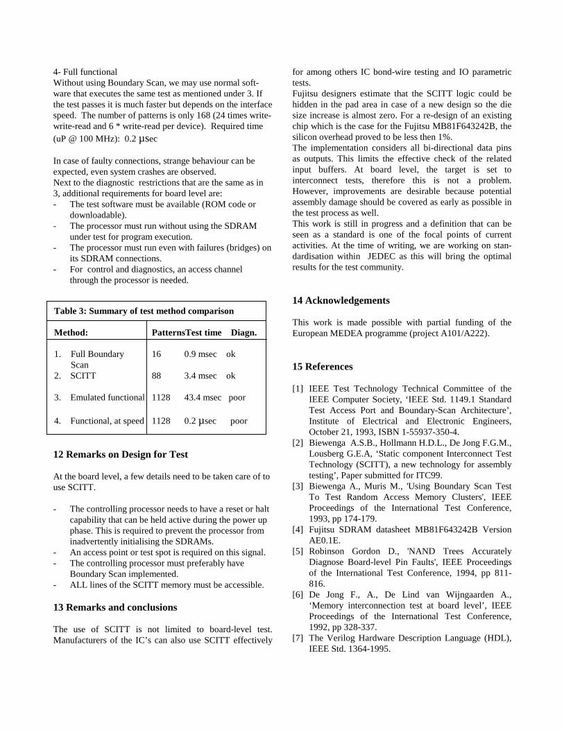
4- Full functionalWithout using Boundary Scan, we may use normal soft-ware that executes the same test as mentioned under 3. Ifthe test passes it is much faster but depends on the interfacespeed. The number of patterns is only 168 (24 times write-write-read and 6 * write-read per device). Required time(uP @ 100 MHz): 0.2 µsec
In case of faulty connections, strange behaviour can beexpected, even system crashes are observed.Next to the diagnostic restrictions that are the same as in3, additional requirements for board level are:- The test software must be available (ROM code or
downloadable).- The processor must run without using the SDRAM
under test for program execution.- The processor must run even with failures (bridges) on
its SDRAM connections.- For control and diagnostics, an access channel
through the processor is needed.
12 Remarks on Design for Test
At the board level, a few details need to be taken care of touse SCITT.
- The controlling processor needs to have a reset or haltcapability that can be held active during the power upphase. This is required to prevent the processor frominadvertently initialising the SDRAMs.
- An access point or test spot is required on this signal.- The controlling processor must preferably have
Boundary Scan implemented.- ALL lines of the SCITT memory must be accessible.
13 Remarks and conclusions
The use of SCITT is not limited to board-level test.Manufacturers of the IC’s can also use SCITT effectively
for among others IC bond-wire testing and IO parametrictests.Fujitsu designers estimate that the SCITT logic could behidden in the pad area in case of a new design so the diesize increase is almost zero. For a re-design of an existingchip which is the case for the Fujitsu MB81F643242B, thesilicon overhead proved to be less then 1%.The implementation considers all bi-directional data pinsas outputs. This limits the effective check of the relatedinput buffers. At board level, the target is set tointerconnect tests, therefore this is not a problem.However, improvements are desirable because potentialassembly damage should be covered as early as possible inthe test process as well.This work is still in progress and a definition that can beseen as a standard is one of the focal points of currentactivities. At the time of writing, we are working on stan-dardisation within JEDEC as this will bring the optimalresults for the test community.
14 Acknowledgements
This work is made possible with partial funding of theEuropean MEDEA programme (project A101/A222).
15 References
[1] IEEE Test Technology Technical Committee of theIEEE Computer Society, ‘IEEE Std. 1149.1 StandardTest Access Port and Boundary-Scan Architecture’,Institute of Electrical and Electronic Engineers,October 21, 1993, ISBN 1-55937-350-4.
[2] Biewenga A.S.B., Hollmann H.D.L., De Jong F.G.M.,Lousberg G.E.A, ‘Static component Interconnect TestTechnology (SCITT), a new technology for assemblytesting’, Paper submitted for ITC99.
[3] Biewenga A., Muris M., 'Using Boundary Scan TestTo Test Random Access Memory Clusters', IEEEProceedings of the International Test Conference,1993, pp 174-179.
[4] Fujitsu SDRAM datasheet MB81F643242B VersionAE0.1E.
[5] Robinson Gordon D., 'NAND Trees AccuratelyDiagnose Board-level Pin Faults', IEEE Proceedingsof the International Test Conference, 1994, pp 811-816.
[6] De Jong F., A., De Lind van Wijngaarden A.,‘Memory interconnection test at board level’, IEEEProceedings of the International Test Conference,1992, pp 328-337.
[7] The Verilog Hardware Description Language (HDL),IEEE Std. 1364-1995.
Table 3: Summary of test method comparison
Method: PatternsTest time Diagn.
1. Full Boundary 16 0.9 msec okScan
2. SCITT 88 3.4 msec ok
3. Emulated functional 1128 43.4 msec poor
4. Functional, at speed 1128 0.2 µsec poor

[8] Jarwala N., Yau C., ‘A New Framework for AnalyzingTest Generation and Diagnosis Algorithms for Wiring
Interconnects’, IEEE proceedings of the InternationalTest Conference, 1989, pp 63-70.
Appendix A: The interconnection test patterns for the 64Mbit SDRAM circuit.
# test patterns for module en20_32# vector# i1 D = input low# i2 U = input high# i3 L = output low# i4 H = output high# i5# i6 i11 i16 o1 o6 o11 o16 o21 o26 o31# i7 i12 i17 o2 o7 o12 o17 o22 o27 o32# i8 i13 i18 o3 o8 o13 o18 o23 o28# i9 i14 i19 o4 o9 o14 o19 o24 o29# i10 i15 i20 o5 o10 o15 o20 o25 o30
1 DDDDDDDDDDDDDDDDDDDDHHHHHHHHHHHHHHHHHHHHHHHHHHHHHHHH # all-0 stimulus 2 UDDDDDDDDDDDDDDDDDDDLLLLLLLLLLLLLLLLLLLHHHHHHHHHHHHH # 20x walking-1 3 DUDDDDDDDDDDDDDDDDDDLHHHHHHHHHHHHHHHHHHLLLLLLLLLLLLL 4 DDUDDDDDDDDDDDDDDDDDHLHHHHHHHHHHHHHHHHHLHHHHHHHHHHHH 5 DDDUDDDDDDDDDDDDDDDDHHLHHHHHHHHHHHHHHHHHLHHHHHHHHHHH 6 DDDDUDDDDDDDDDDDDDDDHHHLHHHHHHHHHHHHHHHHHLHHHHHHHHHH 7 DDDDDUDDDDDDDDDDDDDDHHHHLHHHHHHHHHHHHHHHHHLHHHHHHHHH 8 DDDDDDUDDDDDDDDDDDDDHHHHHLHHHHHHHHHHHHHHHHHLHHHHHHHH 9 DDDDDDDUDDDDDDDDDDDDHHHHHHLHHHHHHHHHHHHHHHHHLHHHHHHH 10 DDDDDDDDUDDDDDDDDDDDHHHHHHHLHHHHHHHHHHHHHHHHHLHHHHHH 11 DDDDDDDDDUDDDDDDDDDDHHHHHHHHLHHHHHHHHHHHHHHHHHLHHHHH 12 DDDDDDDDDDUDDDDDDDDDHHHHHHHHHLHHHHHHHHHHHHHHHHHLHHHH 13 DDDDDDDDDDDUDDDDDDDDHHHHHHHHHHLHHHHHHHHHHHHHHHHHLHHH 14 DDDDDDDDDDDDUDDDDDDDHHHHHHHHHHHLHHHHHHHHHHHHHHHHHLHH 15 DDDDDDDDDDDDDUDDDDDDHHHHHHHHHHHHLHHHHHHHHHHHHHHHHHLH 16 DDDDDDDDDDDDDDUDDDDDHHHHHHHHHHHHHLHHHHHHHHHHHHHHHHHL 17 DDDDDDDDDDDDDDDUDDDDHHHHHHHHHHHHHHLHHHHHHHHHHHHHHHHH 18 DDDDDDDDDDDDDDDDUDDDHHHHHHHHHHHHHHHLHHHHHHHHHHHHHHHH 19 DDDDDDDDDDDDDDDDDUDDHHHHHHHHHHHHHHHHLHHHHHHHHHHHHHHH 20 DDDDDDDDDDDDDDDDDDUDHHHHHHHHHHHHHHHHHLHHHHHHHHHHHHHH 21 DDDDDDDDDDDDDDDDDDDUHHHHHHHHHHHHHHHHHHLHHHHHHHHHHHHH 22 DUUUUUUUUUUUUUUUUUUULLLLLLLLLLLLLLLLLLLHHHHHHHHHHHHH 23 UDUUUUUUUUUUUUUUUUUULHHHHHHHHHHHHHHHHHHLLLLLLLLLLLLL # 20x walking-0 24 UUDUUUUUUUUUUUUUUUUUHLHHHHHHHHHHHHHHHHHLHHHHHHHHHHHH 25 UUUDUUUUUUUUUUUUUUUUHHLHHHHHHHHHHHHHHHHHLHHHHHHHHHHH 26 UUUUDUUUUUUUUUUUUUUUHHHLHHHHHHHHHHHHHHHHHLHHHHHHHHHH 27 UUUUUDUUUUUUUUUUUUUUHHHHLHHHHHHHHHHHHHHHHHLHHHHHHHHH 28 UUUUUUDUUUUUUUUUUUUUHHHHHLHHHHHHHHHHHHHHHHHLHHHHHHHH 29 UUUUUUUDUUUUUUUUUUUUHHHHHHLHHHHHHHHHHHHHHHHHLHHHHHHH 30 UUUUUUUUDUUUUUUUUUUUHHHHHHHLHHHHHHHHHHHHHHHHHLHHHHHH 31 UUUUUUUUUDUUUUUUUUUUHHHHHHHHLHHHHHHHHHHHHHHHHHLHHHHH 32 UUUUUUUUUUDUUUUUUUUUHHHHHHHHHLHHHHHHHHHHHHHHHHHLHHHH 33 UUUUUUUUUUUDUUUUUUUUHHHHHHHHHHLHHHHHHHHHHHHHHHHHLHHH 34 UUUUUUUUUUUUDUUUUUUUHHHHHHHHHHHLHHHHHHHHHHHHHHHHHLHH 35 UUUUUUUUUUUUUDUUUUUUHHHHHHHHHHHHLHHHHHHHHHHHHHHHHHLH 36 UUUUUUUUUUUUUUDUUUUUHHHHHHHHHHHHHLHHHHHHHHHHHHHHHHHL 37 UUUUUUUUUUUUUUUDUUUUHHHHHHHHHHHHHHLHHHHHHHHHHHHHHHHH 38 UUUUUUUUUUUUUUUUDUUUHHHHHHHHHHHHHHHLHHHHHHHHHHHHHHHH 39 UUUUUUUUUUUUUUUUUDUUHHHHHHHHHHHHHHHHLHHHHHHHHHHHHHHH 40 UUUUUUUUUUUUUUUUUUDUHHHHHHHHHHHHHHHHHLHHHHHHHHHHHHHH 41 UUUUUUUUUUUUUUUUUUUDHHHHHHHHHHHHHHHHHHLHHHHHHHHHHHHH
42 UUUUUUUUUUUUUUUUUUUUHHHHHHHHHHHHHHHHHHHHHHHHHHHHHHHH # all-1 stimulus

Appendix B: The Verilog description of the 64Mbit SDRAM SCITT implementation.
module en20_32 (o1,o2,o3,o4,o5,o6,o7,o8,o9,o10,o11,o12,o13, o14,o15,o16,o17,o18,o19,o20,o21,o22,o23,o24, o25,o26,o27,o28,o29,o30,o31,o32, i1,i2,i3,i4,i5,i6,i7,i8,i9,i10,i11,i12,i13, i14,i15,i16,i17,i18,i19,i20);
output o1,o2,o3,o4,o5,o6,o7,o8,o9,o10;output 11,o12,o13,o14,o15,o16,o17,o18,o19,o20;output 21,o22,o23,o24,o25,o26,o27,o28,o29,o30;output o31,o32;input i1,i2,i3,i4,i5,i6,i7,i8,i9,i10;input i11,i12,i13,i14,i15,i16,i17,i18,i19,i20;
xnor #10 (o1, i1, i2); //32 times 2-input xnorxnor #10 (o2, i1, i3);xnor #10 (o3, i1, i4);xnor #10 (o4, i1, i5);xnor #10 (o5, i1, i6);xnor #10 (o6, i1, i7);xnor #10 (o7, i1, i8);xnor #10 (o8, i1, i9);xnor #10 (o9, i1, i10);xnor #10 (o10, i1, i11);xnor #10 (o11, i1, i12);xnor #10 (o12, i1, i13);xnor #10 (o13, i1, i14);xnor #10 (o14, i1, i15);xnor #10 (o15, i1, i16);xnor #10 (o16, i1, i17);xnor #10 (o17, i1, i18);xnor #10 (o18, i1, i19);xnor #10 (o19, i1, i20);xnor #10 (o20, i2, i3);xnor #10 (o21, i2, i4);xnor #10 (o22, i2, i5);xnor #10 (o23, i2, i6);xnor #10 (o24, i2, i7);xnor #10 (o25, i2, i8);xnor #10 (o26, i2, i9);xnor #10 (o27, i2, i10);xnor #10 (o28, i2, i11);xnor #10 (o29, i2, i12);xnor #10 (o30, i2, i13);xnor #10 (o31, i2, i14);xnor #10 (o32, i2, i15);endmodule // en20_32


