Star-Hspice Quick Reference...
290
Star-Hspice Quick Reference Guide Release 2001.4 December 2001
Transcript of Star-Hspice Quick Reference...
Star-HspiceQuick Reference Guide
Release 2001.4December 2001
01
d
f
orr
Star-Hspice Quick Reference Guide, Release 2001.4, December 20Previously printed June 2001, V2001.2Copyright © 2001 Avant! Corporation and Avant! subsidiary. All rightsreserved.Unpublished—rights reserved under the copyright laws of the UniteStates.
Use of copyright notices is precautionary and does not implypublication or disclosure.
DisclaimerAVANT! RESERVES THE RIGHT TO MAKE CHANGES TO ANYPRODUCTS HEREIN WITHOUT FURTHER NOTICE. AVANT!MAKES NO WARRANTY, REPRESENTATION, ORGUARANTEE REGARDING THE FITNESS OF ITS PRODUCTSFOR ANY PARTICULAR PURPOSE AND SPECIFICALLYDISCLAIMS ANY WARRANTY OF MERCHANTABILITY ANDANY WARRANTY OF NON-INFRINGEMENT. AVANT! DOESNOT ASSUME ANY LIABILITY ARISING OUT OF THEAPPLICATION OR USE OF ANY PRODUCT, ANDSPECIFICALLY DISCLAIMS ANY AND ALL LIABILITY,INCLUDING WITHOUT LIMITATION, SPECIAL, INCIDENTALOR CONSEQUENTIAL DAMAGES. AVANT!'S LIABILITYARISING OUT OF THE MANUFACTURE, SALE OR SUPPLYINGOF THE PRODUCTS OR THEIR USE OR DISPOSITION,WHETHER BASED UPON WARRANTY, CONTRACT, TORT OROTHERWISE, SHALL NOT EXCEED THE ACTUAL LICENSEFEE PAID BY CUSTOMER.
Proprietary Rights NoticeThis document contains information of a proprietary nature. No part othis manual may be copied or distributed without the prior writtenconsent of Avant! corporation. This document and the softwaredescribed herein is only provided under a written license agreementa type of written non-disclosure agreement with Avant! corporation oits subsidiaries. ALL INFORMATION CONTAINED HEREINSHALL BE KEPT IN CONFIDENCE AND USED STRICTLY INACCORDANCE WITH THE TERMS OF THE WRITTEN NON-DISCLOSURE AGREEMENT OR WRITTEN LICENSE
ii Star-Hspice Quick Reference Guide

s,S,
r,
s
AGREEMENT WITH AVANT! CORPORATION OR ITSSUBSIDIARIES.
Trademark/Service-Mark NoticeApolloII, ApolloII-GA, Aurora, ASIC Synthesizer, AvanTestchip,AvanWaves, ChipPlanner, Columbia, Columbia-CE, Cyclelink,Davinci, DFM Workbench, Driveline, Dynamic Model Switcher,Electrically Aware, Enterprise, EnterpriseACE, Evaccess, Hercules,Hercules-Explorer, HotPlace, HSPICE, HSPICE-LINK, LTL, Libra-Passport, Lynx, Lynx-LB, Lynx-VHDL, Mars, Mars-Rail, Mars-Xtalk,MASTER Toolbox, Medici, Michelangelo, Milkyway, OptimumSilicon, Passport, Pathfinder, Planet, Planet-PL, Planet-RTL, PolariPolaris-CBS, Polaris-MT, Progen, Prospector, Raphael, Raphael-NESaturn, Sirius, Silicon Blueprint, Smart Extraction, Solar, Solar II, StaStar-Sim, Star-Hspice, Star-HspiceLink, Star-DC, Star-RC, Star-Power, Star-Time, Star-MTB, Star-XP, Taurus, Taurus-Device,Taurus-Layout, Taurus-Lithography, Taurus-OPC, Taurus-Process,Taurus-Topography, Taurus-Visual, Taurus-Workbench, TimeSlice,and TSUPREM-4 are trademarks of Avant! Corporation. Avant!,Avant! logo, AvanLabs, and avanticorp are trademarks and service-marks of Avant! Corporation. All other trademarks and service-markare the property of their respective owners.
Contacting Avant! CorporationTelephone:............ (510) 413-8000Facsimile: ............. (510) 413-8080Toll-Free Telephone:(800) 369-0080URL: ....................http://www.avanticorp.com
Avant! Corporation46871 Bayside ParkwayFremont, CA 94538
Star-Hspice Quick Reference Guide iii
iv Star-Hspice Quick Reference Guide

Star-Hspice Quic
Contents
-1-2-3
-1-2
3-13-2-3-6-8
3-9-10
-1
-1-2-7-8
Chapter 1 - Introduction ................................................. 1-1Syntax Notation ......................................................... 1Common Abbreviations.............................................. 1Input and Output Files ................................................ 1
Chapter 2 - Discrete Device Library (DDL) .................. 2-1DDL Use..................................................................... 2DDL Access................................................................ 2
Chapter 3 - Passive Devices and Independent Sources 3-1Statements................................................................... Resistors...................................................................... Capacitors ................................................................... 3Inductors ..................................................................... 3Magnetics.................................................................... 3Independent Source Element ...................................... Independent Sources................................................. 3
Chapter 4 - Transmission Lines...................................... 4-1W Element Statement ................................................. 4
Chapter 5 - IBIS Conventions......................................... 5-1Buffer Element............................................................ 5Buffers ........................................................................ 5Differential Pins.......................................................... 5Scaling Buffer Strength .............................................. 5
k Reference Guide v
Contents
-1-1-3-3-6125
1-2-3-3
3
7
-1-1-3-3
-1
-2
Chapter 6 - Diodes ........................................................... 6Diode Element ............................................................ 6Junction Model Statement .......................................... 6Junction Model Parameters......................................... 6Juncap Model.............................................................. 6Temperature Effects.................................................. 6-Fowler-Nordheim Diode........................................... 6-1
Chapter 7 - BJT Element ................................................ 7-Bipolar Junction Transistors (BJTs) Element............. 7BJT Model Statement ................................................. 7BJT Model Parameters ............................................... 7LEVEL 6 Philips Bipolar Model ............................. 7-10LEVEL 8 HiCUM Model ......................................... 7-29Level 9 VBIC99 Model ............................................ 7-4Level 10 MODELLA Model .................................... 7-46Level 11 UCSD HBT Model .................................... 7-4
Chapter 8 - Elements ....................................................... 8General Form for Elements ....................................... 8JFET and MESFET Model Statements....................... 8JFET Model Parameters ............................................. 8
Chapter 9 - MOSFET Introduction ............................... 9-1MOSFET Element Statement ..................................... 9
Chapter 10 - MOSFET Models..................................... 10-1Model Table.............................................................. 10LEVEL 47 BSIM3 Version 2 MOS Model .............. 10-6LEVELs 49 and 53 BSIM3v3 MOS Models............ 10-9LEVEL 50 Philips MOS9 Model ........................... 10-10LEVEL 54 BSIM 4.0 Model .................................. 10-11
vi Star-Hspice Quick Reference Guide
1
-1-2
-1-1-8-21
-1-5910103
15
1-2-3
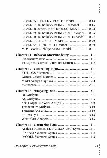
LEVEL 55 EPFL-EKV MOSFET Model............... 10-13LEVEL 57 UC Berkeley BSIM3-SOI Model......... 10-15LEVEL 58 University of Florida SOI Model ......... 10-23LEVEL 59 UC Berkeley BSIM3-SOI FD Model... 10-25LEVEL 60 UC Berkeley BSIM3-SOI DD Model.. 10-27LEVEL 61 RPI a-Si TFT Model ............................ 10-29LEVEL 62 RPI Poli-Si TFT Model........................ 10-30MOS Level 63, Philips MOS11 Model .................. 10-3
Chapter 11 - Behavior Macromodeling ....................... 11-1Subcircuit/Macros..................................................... 11Voltage and Current Controlled Elements................ 11
Chapter 12 - Controlling Input..................................... 12-1.OPTIONS Statement ............................................... 12General Control Options........................................... 12Model Analysis Options ........................................... 12Statements............................................................... 12
Chapter 13 - Analyzing Data ........................................ 13-1DC Analysis.............................................................. 13AC Analysis.............................................................. 13Small-Signal Network Analysis ............................... 13-Temperature Analysis............................................. 13-Transient Analysis .................................................. 13-FFT Analysis .......................................................... 13-1Worst Case Analysis............................................... 13-
Chapter 14 - Optimizing Data ...................................... 14-1Analysis Statement (.DC, .TRAN, .AC) Syntax....... 14-.PARAM Statement Syntax...................................... 14.MODEL Statement Syntax...................................... 14
Star-Hspice Quick Reference Guide vii

Contents
-4-4
-1-4-5
1516178
211
Filters and Systems ................................................... 14Laplace Transforms .................................................. 14
Chapter 15 - Output Format......................................... 15-1Graphing Results in AvanWaves.............................. 15AC Analysis.............................................................. 15Print Commands ....................................................... 15.DOUT Statement ................................................... 15-DC and Transient Output........................................ 15-Power Output .......................................................... 15-AC Analysis Output................................................ 15-1Element Template Output....................................... 15-Element Template Listings ..................................... 15-2
viii Star-Hspice Quick Reference Guide
Star-Hspice Quic
1-
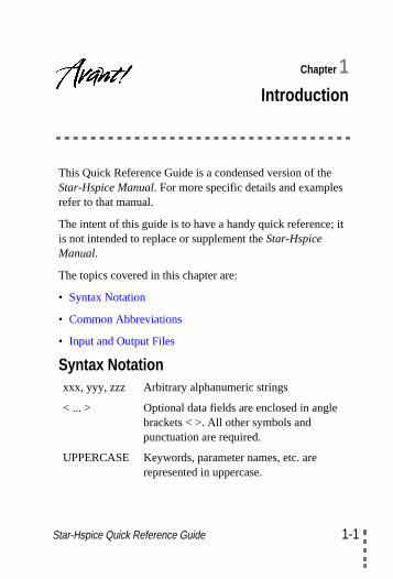
Chapter 1Introduction
it
This Quick Reference Guide is a condensed version of theStar-Hspice Manual. For more specific details and examplesrefer to that manual.
The intent of this guide is to have a handy quick reference;is not intended to replace or supplement theStar-HspiceManual.
The topics covered in this chapter are:
• Syntax Notation
• Common Abbreviations
• Input and Output Files
Syntax Notationxxx, yyy, zzz Arbitrary alphanumeric strings
< ... > Optional data fields are enclosed in anglebrackets < >. All other symbols andpunctuation are required.
UPPERCASE Keywords, parameter names, etc. arerepresented in uppercase.
k Reference Guide 1-1
Introduction
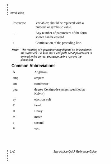
Note: The meaning of a parameter may depend on its location inthe statement. Be sure that a complete set of parameters isentered in the correct sequence before running thesimulation.
Common Abbreviations
lowercase Variables; should be replaced with anumeric or symbolic value.
... Any number of parameters of the formshown can be entered.
+ Continuation of the preceding line.
Å Angstrom
amp ampere
cm centimeter
deg degree Centigrade (unless specified asKelvin)
ev electron volt
F farad
H Henry
m meter
s second
V volt
1-2 Star-Hspice Quick Reference Guide
Input and Output Files
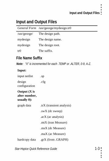
Input and Output Files
File Name SuffixNote: “X” is incremented for each .TEMP or .ALTER, 0-9, A-Z.
General Form /usr/george/mydesign.tr0
/usr/george/ The design path.
mydesign The design name.
mydesign The design root.
tr0 The suffix.
Input:
input netlist .sp
designconfiguration
.cfg
Output (X isalter number,usually 0):
graph data .trX (transient analysis)
.swX (dc sweep)
.acX (ac analysis)
.mtX (tran Measure)
.msX (dc Measure)
.maX (ac Measure)
hardcopy data .grX (from .GRAPH)
Star-Hspice Quick Reference Guide 1-3
Introduction
.
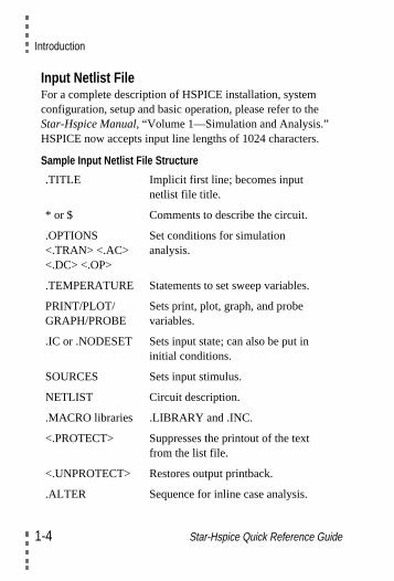
Input Netlist FileFor a complete description of HSPICE installation, systemconfiguration, setup and basic operation, please refer to theStar-Hspice Manual, “Volume 1—Simulation and Analysis.”HSPICE now accepts input line lengths of 1024 characters
Sample Input Netlist File Structure
.TITLE Implicit first line; becomes inputnetlist file title.
* or $ Comments to describe the circuit.
.OPTIONS<.TRAN> <.AC><.DC> <.OP>
Set conditions for simulationanalysis.
.TEMPERATURE Statements to set sweep variables.
PRINT/PLOT/GRAPH/PROBE
Sets print, plot, graph, and probevariables.
.IC or .NODESET Sets input state; can also be put ininitial conditions.
SOURCES Sets input stimulus.
NETLIST Circuit description.
.MACRO libraries .LIBRARY and .INC.
<.PROTECT> Suppresses the printout of the textfrom the list file.
<.UNPROTECT> Restores output printback.
.ALTER Sequence for inline case analysis.
1-4 Star-Hspice Quick Reference Guide

Input and Output Files
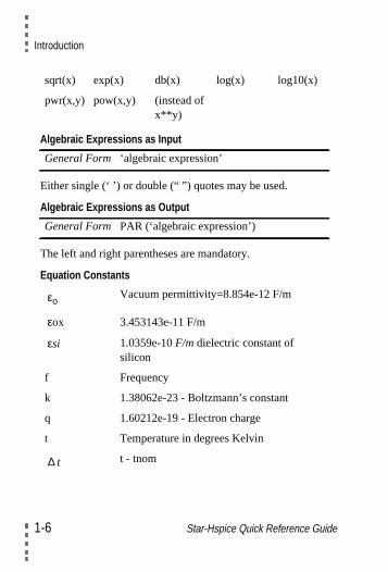
Numeric Scale FactorsA number may be an integer, a floating point number, aninteger or floating point number followed by an integerexponent, or an integer or floating point number followed byone of the scale factors listed below.
Algebraic ExpressionsIn addition to simple arithmetic operations (+, -, *, /), thefollowing quoted string functions may be used:
.PARAMETER Redefinition.
.END Terminates any ALTERs and thesimulation.
F =1e-15
P =1e-12
N =1e-9
U =1e-6
M =1e-3
K =1e3
MEG (or X) =1e6
MI =25.4e6
G =1e9
sin(x) sinh(x) abs(x) cos(x) cosh(x)
min(x,y) tan(x) tanh(x) max(x,y) atan(x)
Star-Hspice Quick Reference Guide 1-5
Introduction
Algebraic Expressions as Input
Either single (‘ ’) or double (“ ”) quotes may be used.
Algebraic Expressions as Output
The left and right parentheses are mandatory.
Equation Constants
sqrt(x) exp(x) db(x) log(x) log10(x)
pwr(x,y) pow(x,y) (instead ofx**y)
General Form ‘algebraic expression’
General Form PAR (‘algebraic expression’)
Vacuum permittivity=8.854e-12 F/m
3.453143e-11 F/m
1.0359e-10F/m dielectric constant ofsilicon
f Frequency
k 1.38062e-23 - Boltzmann’s constant
q 1.60212e-19 - Electron charge
t Temperature in degrees Kelvin
t t - tnom
εo
εox
εsi
∆
1-6 Star-Hspice Quick Reference Guide
Input and Output Files
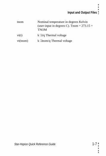
tnom Nominal temperature in degrees Kelvin(user-input in degrees C). Tnom = 273.15 +TNOM
vt(t) k ⋅ t/q Thermal voltage
vt(tnom) k ⋅ tnom/q Thermal voltage
Star-Hspice Quick Reference Guide 1-7
Introduction
1-8 Star-Hspice Quick Reference Guide
Star-Hspice Quic
2-
Chapter 2Discrete Device Library (DDL)
d),
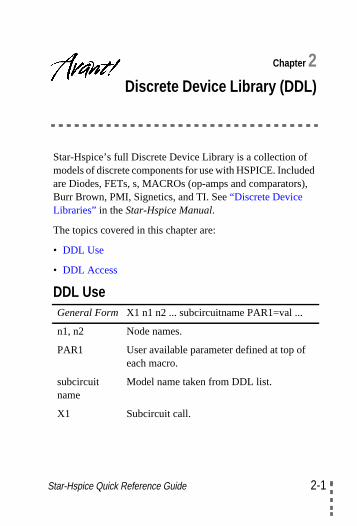
Star-Hspice’s full Discrete Device Library is a collection ofmodels of discrete components for use with HSPICE. Includeare Diodes, FETs, s, MACROs (op-amps and comparatorsBurr Brown, PMI, Signetics, and TI. See“Discrete DeviceLibraries” in theStar-Hspice Manual.
The topics covered in this chapter are:
• DDL Use
• DDL Access
DDL UseGeneral Form X1 n1 n2 ... subcircuitname PAR1=val ...
n1, n2 Node names.
PAR1 User available parameter defined at top ofeach macro.
subcircuitname
Model name taken from DDL list.
X1 Subcircuit call.
k Reference Guide 2-1
Discrete Device Library (DDL)
ry
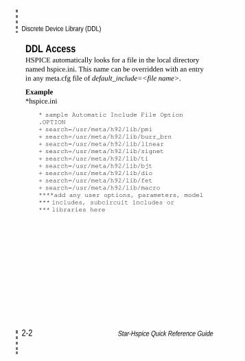
DDL AccessHSPICE automatically looks for a file in the local directorynamed hspice.ini. This name can be overridden with an entin any meta.cfg file ofdefault_include=<file name>.
Example*hspice.ini
* sample Automatic Include File Option.OPTION+ search=/usr/meta/h92/lib/pmi+ search=/usr/meta/h92/lib/burr_brn+ search=/usr/meta/h92/lib/linear+ search=/usr/meta/h92/lib/signet+ search=/usr/meta/h92/lib/ti+ search=/usr/meta/h92/lib/bjt+ search=/usr/meta/h92/lib/dio+ search=/usr/meta/h92/lib/fet+ search=/usr/meta/h92/lib/macro****add any user options, parameters, model*** includes, subcircuit includes or*** libraries here
2-2 Star-Hspice Quick Reference Guide

Star-Hspice Quic
3-
Chapter 3Passive Devices and
Independent Sources
ce
The topics covered in this chapter are:
• Statements
• Resistors
• Capacitors
• Inductors
• Magnetics
• Independent Source Element
• Independent Sources
The passive devices and independent sources in Star-Hspican use the following.
StatementsElement StatementGeneral Form NAME node1,node2 … nodeN
+ <model reference> value+ <optional parameters>
k Reference Guide 3-1
Passive Devices and Independent Sources
e
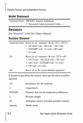
Model Statement
ResistorsSee“Resistors” in theStar-Hspice Manual.
Resistor Element
If mname is specified, the resistor value specification would boptional.
General Form .MODEL mname modeltype+ <keyword=value keyword=value...>
General Form Rxxx n1 n2 <mname> Rval <TC1 <TC2>>+ <SCALE=val> <M=val> <AC=val>+ <DTEMP=val> <L=val> <W=val>+ <C=val>
Or Rxxx n1 n2 <mname> R=val <TC1=val>+ <TC2=val> <SCALE=val> <M=val>+ <AC=val> <DTEMP=val> <L=val>+ <W=val> <C=val>
Or Rxxx n1 n2 R=‘users defined equation’
AC Resistance for AC analysis
C Capacitance
DTEMP Element and circuit temperature difference
L Resistor length
M Multiplier used to simulate parallel resistors
mname Model name
3-2 Star-Hspice Quick Reference Guide
Capacitors
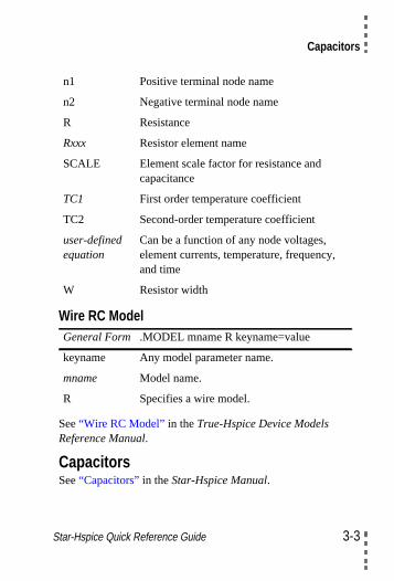
Wire RC Model
See“Wire RC Model” in theTrue-Hspice Device ModelsReference Manual.
CapacitorsSee“Capacitors” in theStar-Hspice Manual.
n1 Positive terminal node name
n2 Negative terminal node name
R Resistance
Rxxx Resistor element name
SCALE Element scale factor for resistance andcapacitance
TC1 First order temperature coefficient
TC2 Second-order temperature coefficient
user-definedequation
Can be a function of any node voltages,element currents, temperature, frequency,and time
W Resistor width
General Form .MODEL mname R keyname=value
keyname Any model parameter name.
mname Model name.
R Specifies a wire model.
Star-Hspice Quick Reference Guide 3-3
Passive Devices and Independent Sources
s
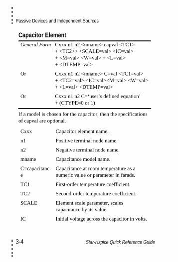
Capacitor Element
If a model is chosen for the capacitor, then the specificationof capval are optional.
General Form Cxxx n1 n2 <mname> capval <TC1>+ <TC2>> <SCALE=val> <IC=val>+ <M=val> <W=val> + <L=val>+ <DTEMP=val>
Or Cxxx n1 n2 <mname> C=val <TC1=val>+ <TC2=val> <IC=val><M=val> <W=val>+ <L=val> <DTEMP=val>
Or Cxxx n1 n2 C=‘user’s defined equation’+ (CTYPE=0 or 1)
Cxxx Capacitor element name.
n1 Positive terminal node name.
n2 Negative terminal node name.
mname Capacitance model name.
C=capacitance
Capacitance at room temperature as anumeric value or parameter in farads.
TC1 First-order temperature coefficient.
TC2 Second-order temperature coefficient.
SCALE Element scale parameter, scalescapacitance by its value.
IC Initial voltage across the capacitor in volts.
3-4 Star-Hspice Quick Reference Guide
Capacitors
ter
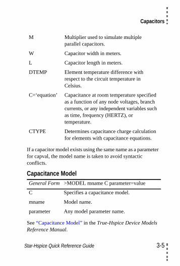
If a capacitor model exists using the same name as a paramefor capval, the model name is taken to avoid syntacticconflicts.Capacitance Model
See“Capacitance Model” in theTrue-Hspice Device ModelsReference Manual.
M Multiplier used to simulate multipleparallel capacitors.
W Capacitor width in meters.
L Capacitor length in meters.
DTEMP Element temperature difference withrespect to the circuit temperature inCelsius.
C=‘equation’ Capacitance at room temperature specifiedas a function of any node voltages, branchcurrents, or any independent variables suchas time, frequency (HERTZ), ortemperature.
CTYPE Determines capacitance charge calculationfor elements with capacitance equations.
General Form >MODEL mname C parameter=value
C Specifies a capacitance model.
mname Model name.
parameter Any model parameter name.
Star-Hspice Quick Reference Guide 3-5
Passive Devices and Independent Sources
.
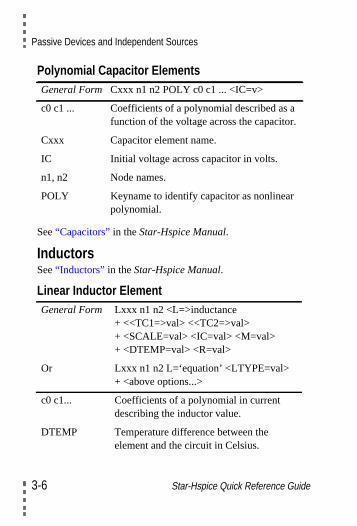
Polynomial Capacitor Elements
See“Capacitors” in theStar-Hspice Manual.
InductorsSee“Inductors” in theStar-Hspice Manual.
Linear Inductor Element
General Form Cxxx n1 n2 POLY c0 c1 ... <IC=v>
c0 c1 ... Coefficients of a polynomial described as afunction of the voltage across the capacitor
Cxxx Capacitor element name.
IC Initial voltage across capacitor in volts.
n1, n2 Node names.
POLY Keyname to identify capacitor as nonlinearpolynomial.
General Form Lxxx n1 n2 <L=>inductance+ <<TC1=>val> <<TC2=>val>+ <SCALE=val> <IC=val> <M=val>+ <DTEMP=val> <R=val>
Or Lxxx n1 n2 L=‘equation’ <LTYPE=val>+ <above options...>
c0 c1... Coefficients of a polynomial in currentdescribing the inductor value.
DTEMP Temperature difference between theelement and the circuit in Celsius.
3-6 Star-Hspice Quick Reference Guide
Inductors
Mutual Inductor Element
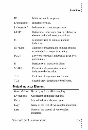
IC Initial current in amperes.
L=inductance Inductance value.
L=‘equation’ Inductance at room temperature.
LTYPE Determines inductance flux calculation forelements with inductance equations.
M Multiplier used to simulate parallelinductors.
NT=turns Number representing the number of turnsof an inductive magnetic winding.
POLY Keyword to specify inductance given by apolynomial.
R Resistance of inductor in ohms.
SCALE Element scale parameter; scalesinductance by its value.
TC1 First-order temperature coefficient.
TC2 Second-order temperature coefficient.
General Form Kxxx Lyyy Lzzz <K=>coupling
K=coupling Coefficient of mutual coupling.
Kxxx Mutual inductor element name.
Lyyy Name of the first of two coupled inductors.
Lzzz Name of the second of two coupledinductors.
Star-Hspice Quick Reference Guide 3-7
Passive Devices and Independent Sources
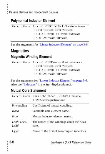
Polynomial Inductor Element
See the arguments for“Linear Inductor Element” on page 3-6.
MagneticsMagnetic Winding Element
See the arguments for“Linear Inductor Element” on page 3-6.Also see“Inductors” in theStar-Hspice Manual.
Mutual Core Statement
General Form Lxxx n1 n2 POLYc0 c1 <L=>inductance+ <<TC1=>val> <<TC2=>val>+ <SCALE=val> <IC=val> <M=val>+ <DTEMP=val> <R=val>
General Form Lxxx n1 n2 NT=turns <L=>inductance+ <<TC1=>val> <<TC2=>val>+ <SCALE=val> <IC=val> <M=val>+ <DTEMP=val> <R=val>
General Form Kaaa Lbbb <Lccc ... <Lddd>> mname+ <MAG=magnetization>
K=coupling Coefficient of mutual coupling.
Kaaa Saturable core element name.
Kxxx Mutual inductor element name.
Lbbb, Lccc,Lddd
The names of the windings about the Kaaacore.
Lyyy Name of the first of two coupled inductors.
3-8 Star-Hspice Quick Reference Guide
Independent Source Element
See“Inductors” in theStar-Hspice Manual.
Magnetic Core Model
See“Magnetic Core Syntax” in theTrue-Hspice DeviceModels Reference Manual.
Independent Source Element
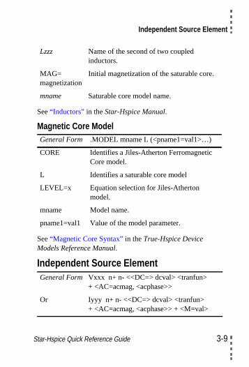
Lzzz Name of the second of two coupledinductors.
MAG=magnetization
Initial magnetization of the saturable core.
mname Saturable core model name.
General Form .MODEL mname L (<pname1=val1>…)
CORE Identifies a Jiles-Atherton FerromagneticCore model.
L Identifies a saturable core model
LEVEL=x Equation selection for Jiles-Athertonmodel.
mname Model name.
pname1=val1 Value of the model parameter.
General Form Vxxx n+ n- <<DC=> dcval> <tranfun>+ <AC=acmag, <acphase>>
Or Iyyy n+ n- <<DC=> dcval> <tranfun>+ <AC=acmag, <acphase>> + <M=val>
Star-Hspice Quick Reference Guide 3-9
Passive Devices and Independent Sources
See“Independent Source Element” in theStar-HspiceManual.
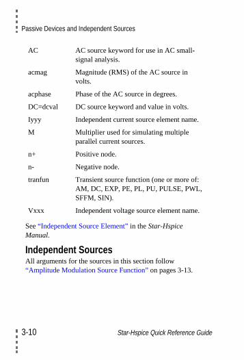
Independent SourcesAll arguments for the sources in this section follow“Amplitude Modulation Source Function” on pages 3-13.
AC AC source keyword for use in AC small-signal analysis.
acmag Magnitude (RMS) of the AC source involts.
acphase Phase of the AC source in degrees.
DC=dcval DC source keyword and value in volts.
Iyyy Independent current source element name.
M Multiplier used for simulating multipleparallel current sources.
n+ Positive node.
n- Negative node.
tranfun Transient source function (one or more of:AM, DC, EXP, PE, PL, PU, PULSE, PWL,SFFM, SIN).
Vxxx Independent voltage source element name.
3-10 Star-Hspice Quick Reference Guide
Independent Sources
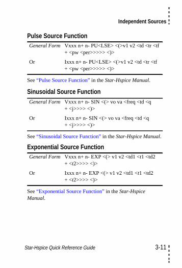
Pulse Source Function
See“Pulse Source Function” in theStar-Hspice Manual.
Sinusoidal Source Function
See“Sinusoidal Source Function”in theStar-Hspice Manual.
Exponential Source Function
See“Exponential Source Function” in theStar-HspiceManual.
General Form Vxxx n+ n- PU<LSE> <(>v1 v2 <td <tr <tf+ <pw <per>>>>> <)>
Or Ixxx n+ n- PU<LSE> <(>v1 v2 <td <tr <tf+ <pw <per>>>>> <)>
General Form Vxxx n+ n- SIN <(> vo va <freq <td <q+ <j>>>> <)>
Or Ixxx n+ n- SIN <(> vo va <freq <td <q+ <j>>>> <)>
General Form Vxxx n+ n- EXP <(> v1 v2 <td1 <t1 <td2+ <t2>>>> <)>
Or Ixxx n+ n- EXP <(> v1 v2 <td1 <t1 <td2+ <t2>>>> <)>
Star-Hspice Quick Reference Guide 3-11
Passive Devices and Independent Sources
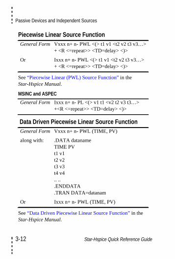
Piecewise Linear Source Function
See“Piecewise Linear (PWL) Source Function” in theStar-Hspice Manual.
MSINC and ASPEC
Data Driven Piecewise Linear Source Function
See“Data Driven Piecewise Linear Source Function” in theStar-Hspice Manual.
General Form Vxxx n+ n- PWL <(> t1 v1 <t2 v2 t3 v3…>+ <R <=repeat>> <TD=delay> <)>
Or Ixxx n+ n- PWL <(> t1 v1 <t2 v2 t3 v3…>+ <R <=repeat>> <TD=delay> <)>
General Form Ixxx n+ n- PL <(> v1 t1 <v2 t2 v3 t3…>+<R <=repeat>> <TD=delay> <)>
General Form Vxxx n+ n- PWL (TIME, PV)
along with: .DATA datanameTIME PVt1 v1t2 v2t3 v3t4 v4.. ...ENDDATA.TRAN DATA=datanam
Or Ixxx n+ n- PWL (TIME, PV)
3-12 Star-Hspice Quick Reference Guide
Independent Sources
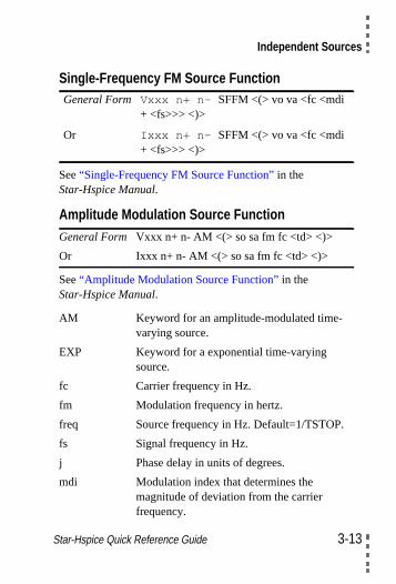
Single-Frequency FM Source Function
See“Single-Frequency FM Source Function” in theStar-Hspice Manual.
Amplitude Modulation Source Function
See“Amplitude Modulation Source Function” in theStar-Hspice Manual.
General Form Vxxx n+ n- SFFM <(> vo va <fc <mdi+ <fs>>> <)>
Or Ixxx n+ n- SFFM <(> vo va <fc <mdi+ <fs>>> <)>
General Form Vxxx n+ n- AM <(> so sa fm fc <td> <)>
Or Ixxx n+ n- AM <(> so sa fm fc <td> <)>
AM Keyword for an amplitude-modulated time-varying source.
EXP Keyword for a exponential time-varyingsource.
fc Carrier frequency in Hz.
fm Modulation frequency in hertz.
freq Source frequency in Hz. Default=1/TSTOP.
fs Signal frequency in Hz.
j Phase delay in units of degrees.
mdi Modulation index that determines themagnitude of deviation from the carrierfrequency.
Star-Hspice Quick Reference Guide 3-13
Passive Devices and Independent Sources
d
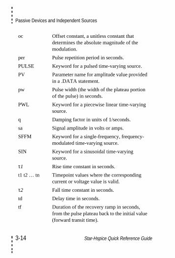
oc Offset constant, a unitless constant thatdetermines the absolute magnitude of themodulation.
per Pulse repetition period in seconds.
PULSE Keyword for a pulsed time-varying source.
PV Parameter name for amplitude value providein a .DATA statement.
pw Pulse width (the width of the plateau portionof the pulse) in seconds.
PWL Keyword for a piecewise linear time-varyingsource.
q Damping factor in units of 1/seconds.
sa Signal amplitude in volts or amps.
SFFM Keyword for a single-frequency, frequency-modulated time-varying source.
SIN Keyword for a sinusoidal time-varyingsource.
τ1 Rise time constant in seconds.
t1 t2 … tn Timepoint values where the correspondingcurrent or voltage value is valid.
τ2 Fall time constant in seconds.
td Delay time in seconds.
tf Duration of the recovery ramp in seconds,from the pulse plateau back to the initial value(forward transit time).
3-14 Star-Hspice Quick Reference Guide
Independent Sources
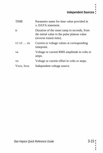
TIME Parameter name for time value provided ina .DATA statement.
tr Duration of the onset ramp in seconds, fromthe initial value to the pulse plateau value(reverse transit time).
v1 v2 … vn Current or voltage values at correspondingtimepoint.
va Voltage or current RMS amplitude in volts oramps.
vo Voltage or current offset in volts or amps.
Vxxx, Ixxx Independent voltage source.
Star-Hspice Quick Reference Guide 3-15
Passive Devices and Independent Sources
3-16 Star-Hspice Quick Reference Guide
Star-Hspice Quic
4-
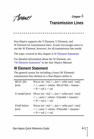
Chapter 4Transmission Lines
tos.
Star-Hspice supports the T Element, U Element, andW Element for transmission lines. Avant! encourages usersuse the W Element, however, for all transmission line need
The topic covered in this chapter isW Element Statement.
For detailed information about the W Element, see“W Element Statement” in theStar-Hspice Manual.
W Element StatementThe general syntax for including a lossy (W Element)transmission line element in a Star-Hspice netlist is:
RLGC fileform
Wxxx in1 <in2 <...inx>> refin out1 <out2+ <...outx>> refout <RLGCfile = fname>+ N = val L = val
U-model form Wxxx in1 <in2 <...inx>> refin out1 <out2+ <...outx>> refout <Umodel = mname>+ N = val L = val
Field Solverform
Wxxx in1 <in2 <...inx>> refin out1 <out2+ <...outx>> refout <FSmodel = mname>+ N = val L = val
k Reference Guide 4-1
Transmission Lines
ot
th
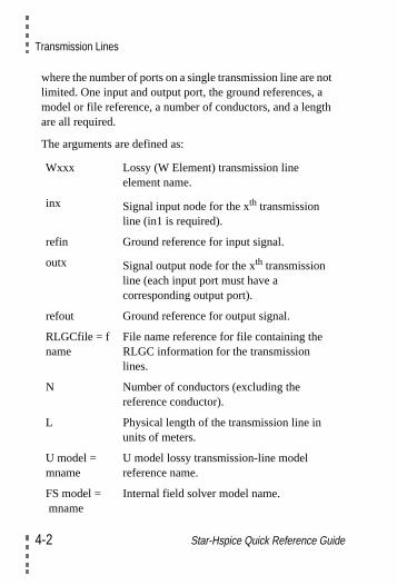
where the number of ports on a single transmission line are nlimited. One input and output port, the ground references, amodel or file reference, a number of conductors, and a lengare all required.
The arguments are defined as:
Wxxx Lossy (W Element) transmission lineelement name.
inx Signal input node for the xth transmissionline (in1 is required).
refin Ground reference for input signal.
outx Signal output node for the xth transmissionline (each input port must have acorresponding output port).
refout Ground reference for output signal.
RLGCfile = fname
File name reference for file containing theRLGC information for the transmissionlines.
N Number of conductors (excluding thereference conductor).
L Physical length of the transmission line inunits of meters.
U model =mname
U model lossy transmission-line modelreference name.
FS model =mname
Internal field solver model name.
4-2 Star-Hspice Quick Reference Guide

Star-Hspice Quic
5-
Chapter 5IBIS Conventions
The topics covered in this chapter are:
• Buffer Element• Buffers• Differential Pins• Scaling Buffer Strength
For detailed information about IBIS conventions, see“Understanding IBIS Conventions”in theTrue-Hspice DeviceModels Reference Manual.
Buffer ElementThe general syntax of an element card for I/O buffers is:
General Form bname node_1 node_2 ... node_N+ keyword_1=value_1 ... or+ [keyword_M=value_M]
bname Buffer element name.
keyword_i =value_i
Assigns value,value_i, to the keyword,keyword_i.Optional keywords are given insquare brackets.
k Reference Guide 5-1
IBIS Conventions
Limitations and RestrictionsThe series, series switch, and terminator buffers are notimplemented in the 00.4 version of Star-Hspice.
You can simulate the terminator by using other existingStar-Hspice elements: resistors, capacitors, and voltagedependent current sources.
For details, see“Limitations and Restrictions” in theTrue-Hspice Device Models Reference Manual.
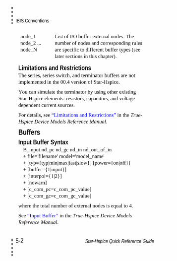
BuffersInput Buffer Syntax
B_input nd_pc nd_gc nd_in nd_out_of_in+ file='filename' model='model_name'+ [typ={typ|min|max|fast|slow}] [power={on|off}]+ [buffer={1|input}]+ [interpol={1|2}]+ [nowarn]+ [c_com_pc=c_com_pc_value]+ [c_com_gc=c_com_gc_value]
where the total number of external nodes is equal to 4.
See“Input Buffer” in theTrue-Hspice Device ModelsReference Manual.
node_1node_2 ...node_N
List of I/O buffer external nodes. Thenumber of nodes and corresponding rulesare specific to different buffer types (seelater sections in this chapter).
5-2 Star-Hspice Quick Reference Guide
Buffers
]
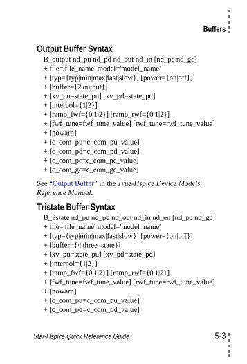
Output Buffer SyntaxB_output nd_pu nd_pd nd_out nd_in [nd_pc nd_gc]+ file='file_name' model='model_name'+ [typ={typ|min|max|fast|slow}] [power={on|off}]+ [buffer={2|output}]+ [xv_pu=state_pu] [xv_pd=state_pd]+ [interpol={1|2}]+ [ramp_fwf={0|1|2}] [ramp_rwf={0|1|2}]+ [fwf_tune=fwf_tune_value] [rwf_tune=rwf_tune_value]+ [nowarn]+ [c_com_pu=c_com_pu_value]+ [c_com_pd=c_com_pd_value]+ [c_com_pc=c_com_pc_value]+ [c_com_gc=c_com_gc_value]
See“Output Buffer” in theTrue-Hspice Device ModelsReference Manual.
Tristate Buffer SyntaxB_3state nd_pu nd_pd nd_out nd_in nd_en [nd_pc nd_gc+ file='file_name' model='model_name'+ [typ={typ|min|max|fast|slow}] [power={on|off}]+ [buffer={4|three_state}]+ [xv_pu=state_pu] [xv_pd=state_pd]+ [interpol={1|2}]+ [ramp_fwf={0|1|2}] [ramp_rwf={0|1|2}]+ [fwf_tune=fwf_tune_value] [rwf_tune=rwf_tune_value]+ [nowarn]+ [c_com_pu=c_com_pu_value]+ [c_com_pd=c_com_pd_value]
Star-Hspice Quick Reference Guide 5-3
IBIS Conventions
c
up
+ [c_com_pc=c_com_pc_value]+ [c_com_gc=c_com_gc_value]
See“Tristate Buffer” in theTrue-Hspice Device ModelsReference Manual.
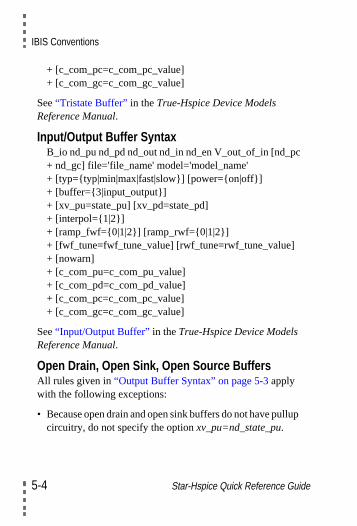
Input/Output Buffer SyntaxB_io nd_pu nd_pd nd_out nd_in nd_en V_out_of_in [nd_p+ nd_gc] file='file_name' model='model_name'+ [typ={typ|min|max|fast|slow}] [power={on|off}]+ [buffer={3|input_output}]+ [xv_pu=state_pu] [xv_pd=state_pd]+ [interpol={1|2}]+ [ramp_fwf={0|1|2}] [ramp_rwf={0|1|2}]+ [fwf_tune=fwf_tune_value] [rwf_tune=rwf_tune_value]+ [nowarn]+ [c_com_pu=c_com_pu_value]+ [c_com_pd=c_com_pd_value]+ [c_com_pc=c_com_pc_value]+ [c_com_gc=c_com_gc_value]
See“Input/Output Buffer”in theTrue-Hspice Device ModelsReference Manual.
Open Drain, Open Sink, Open Source BuffersAll rules given in“Output Buffer Syntax” on page 5-3 applywith the following exceptions:
• Because open drain and open sink buffers do not have pullcircuitry, do not specify the optionxv_pu=nd_state_pu.
5-4 Star-Hspice Quick Reference Guide
Buffers
• Similarly, because open source buffers do not havepulldown circuitry, do not specify the optionxv_pd=nd_state_pd.
See“Open Drain, Open Sink, Open Source Buffers” in theTrue-Hspice Device Models Reference Manual.
I/O Open Drain, I/O Open Sink, I/O Open SourceBuffersAll rules given in“Input/Output Buffer Syntax” on page 5-4apply with the following exceptions:
• Because I/O open drain and I/O open sink buffers do nothave pullup circuitry, do not specify the optionxv_pu=nd_state_pu.
• Similarly, because I/O open source buffers do not havepulldown circuitry, do not specify the optionxv_pd=nd_state_pd.
See“I/O Open Drain, I/O Open Sink, I/O Open SourceBuffers” in theTrue-Hspice Device Models ReferenceManual.
Input ECL Buffer SyntaxB_input_ecl nd_pc nd_gc nd_in nd_out_of_in+ file='file_name' model='model_name'+ [typ={typ|min|max|fast|slow}] [power={on|off}]+ [buffer={11|input_ecl}]+ [interpol={1|2}]+ [nowarn]+ [c_com_pc=c_com_pc_value]+ [c_com_gc=c_com_gc_value]
Star-Hspice Quick Reference Guide 5-5
IBIS Conventions
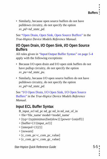
See“Input ECL Buffer” in theTrue-Hspice Device ModelsReference Manual.
Output ECL Buffer SyntaxB_output_ecl nd_pu nd_out nd_in [nd_pc nd_gc]+ file='file_name' model='model_name'+ [typ={typ|min|max|fast|slow}] [power={on|off}]+ [buffer={12|output_ecl}]+ [xv_pu=state_pu] [xv_pd=state_pd]+ [interpol={1|2}]+ [ramp_fwf={0|1|2}] [ramp_rwf={0|1|2}]+ [fwf_tune=fwf_tune_value] [rwf_tune=rwf_tune_value]+ [nowarn]+ [c_com_pu=c_com_pu_value]+ [c_com_pc=c_com_pc_value]+ [c_com_gc=c_com_gc_value]
See“Output ECL Buffer” in theTrue-Hspice Device ModelsReference Manual.
Tristate ECL Buffer SyntaxB_3state_ecl nd_pu nd_out nd_in nd_en [nd_pc nd_gc]+ file='file_name' model='model_name'+ [typ={typ|min|max|fast|slow}] [power={on|off}]+ [buffer={14|three_state_ecl}]+ [xv_pu=state_pu] [xv_pd=state_pd]+ [interpol={1|2}]+ [ramp_fwf={0|1|2}] [ramp_rwf={0|1|2}]+ [fwf_tune=fwf_tune_value] [rwf_tune=rwf_tune_value]+ [nowarn]+ [c_com_pu=c_com_pu_value]
5-6 Star-Hspice Quick Reference Guide
Differential Pins
+ [c_com_pc=c_com_pc_value]+ [c_com_gc=c_com_gc_value]
See“Tristate ECL Buffer”in theTrue-Hspice Device ModelsReference Manual.
Input-Output ECL Buffer SyntaxB_io_ecl nd_pu nd_out nd_in nd_en nd_out_of_in [nd_pc+ nd_gc] file='file_name' model='model_name'+ [typ={typ|min|max|fast|slow}] [power={on|off}]+ [buffer={13|io_ecl}]+ [xv_pu=state_pu] [xv_pd=state_pd]+ [interpol={1|2}]+ [ramp_fwf={0|1|2}] [ramp_rwf={0|1|2}]+ Input-Output ECL Buffer
See“Input-Output ECL Buffer” in theTrue-Hspice DeviceModels Reference Manual.
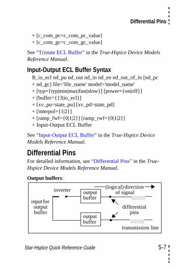
Differential PinsFor detailed information, see“Differential Pins” in theTrue-Hspice Device Models Reference Manual.
Output buffers:
differentialpins
(logical) directionof signaloutput
buffer
outputbuffer
transmission line
inverter
input foroutputbuffer
Star-Hspice Quick Reference Guide 5-7

IBIS Conventions
a
Input buffers:
Scaling Buffer StrengthSometimes you need to scale buffer strength to enable thesame IBIS file to be used to simulate buffers of differentstrengths. K is the factor for current multiplication; for theoriginal buffer, the value of K=1. This section describes howto scale using the F Element for a single output buffer and differential output buffer. For detailed information, see“Scaling Buffer Strength” in theTrue-Hspice Device ModelsReference Manual.
Original Circuit for a Single Output BufferBuffer nd_pu nd_pd nd_out nd_pc nd_gc+ file=<filename> model=<modelname>+ Rload nd_out gnd Rload_val
Scaled Circuit for a Single Output BufferBuffer nd_pu nd_pd nd_out nd_pc nd_gc+ file=<filename> model=<modelname>Vsenser+ nd_out nd_out_prime V=0 Rload nd_out_prime+ gnd Rload_val Felement gnd nd_out_prime+ Vsenser K-1
nd_in_1
(logical) directionof signal
out_of_in_1
out_of_in_2nd_in_2
differentialpins
outputbuffer
outputbuffer
transmission line
transmission line
5-8 Star-Hspice Quick Reference Guide

Scaling Buffer Strength
Original Circuit for a Differential Output BufferBuffer1 nd_pu1 nd_pd1 nd_out1 nd_pc1 nd_gc1+ file=<filename1> model=<modelname1>Buffer2 nd_pu2 nd_pd2 nd_out2 nd_pc2 nd_gc2+ file=<filename2> model=<modelname2> R_load+ n_out1 n_out2 R_load_value
Scaled Circuit for a Differential Output BufferBuffer1 nd_pu1 nd_pd1 nd_out1 nd_pc1 nd_gc1+ file=<filename1> model=<modelname1>Buffer2 nd_pu2 nd_pd2 nd_out2 nd_pc2 nd_gc2+ file=<filename2> model=<modelname2> V_sense+ n_out1 n_out1_prime 0V F_element n_out2+ n_out1_prime v_sense K-1 R_load n_out1_prime+ n_out2 R_load_value
Star-Hspice Quick Reference Guide 5-9
IBIS Conventions
5-10 Star-Hspice Quick Reference Guide
Star-Hspice Quic
6-
Chapter 6Diodes
The topics covered in this chapter are:
• Diode Element
• Junction Model Statement
• Junction Model Parameters
• Juncap Model
• Temperature Effects
• Fowler-Nordheim Diode
Diode ElementGeneral Form Dxxx nplus nminus mname
+ <<AREA = >area> <<PJ = >val>+ <WP = val> <LP = val> <WM = val>+ <LM = val> <OFF> <IC = vd>+ <M = val> <DTEMP = val>
Or Dxxx nplus nminus mname <W = width>+ <L = length> <WP = val> <LP = val>+ <WM = val> <LM = val> <OFF>+ <IC = vd> <M = val> <DTEMP = val>
AREA Area of the diode.
k Reference Guide 6-1
Diodes
DTEMP The difference between the elementtemperature and the circuit temperature inCelsius.
Dxxx Diode element name.
IC = vd Initial voltage across the diode element.
L Length of the diode in meters (diode modelLEVEL = 3 only).
LM Width of metal capacitor in meters (for diodemodel LEVEL = 3 only).
LP Length of polysilicon capacitor in meters (fordiode model LEVEL = 3 only).
M Multiplier to simulate multiple diodes inparallel.
mname Diode model name reference.
nminus Negative terminal (cathode) node name.
nplus Positive terminal (anode) node name.
OFF Sets initial condition to OFF for this elementin DC analysis.
PJ Periphery of junction.
W Width of the diode in meters (diode modelLEVEL = 3 only).
WM Width of metal capacitor in meters (for diodemodel LEVEL = 3 only).
6-2 Star-Hspice Quick Reference Guide
Junction Model Statement
l
See “Diode Element” in Chapter 3, Diodes, in theTrue-HspiceDevice Models Reference Manual.
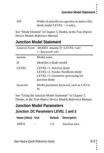
Junction Model Statement
See “Using the Junction Model Statement” in Chapter 3,Diodes, in theTrue-Hspice Device Models Reference Manua.
Junction Model ParametersJunction .DC Parameters LEVEL 1 and 3
WP Width of polysilicon capacitor in meters (fordiode model LEVEL = 3 only).
General Form .MODEL mname D <LEVEL=val>+ <keyword=val>
mname Model name
D Identifies a diode model
LEVEL LEVEL=1: Junction diodeLEVEL=2: Fowler-Nordheim diodeLEVEL=3: Geometric processing forjunction diode
keyword Model parameter keyword, such as CJO orIS
Name (Alias) Unit Default Description
AREA - 1.0 Junction area.
Star-Hspice Quick Reference Guide 6-3
Diodes
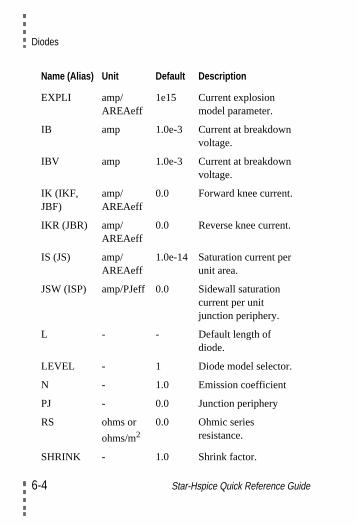
EXPLI amp/AREAeff
1e15 Current explosionmodel parameter.
IB amp 1.0e-3 Current at breakdownvoltage.
IBV amp 1.0e-3 Current at breakdownvoltage.
IK (IKF,JBF)
amp/AREAeff
0.0 Forward knee current.
IKR (JBR) amp/AREAeff
0.0 Reverse knee current.
IS (JS) amp/AREAeff
1.0e-14 Saturation current perunit area.
JSW (ISP) amp/PJeff 0.0 Sidewall saturationcurrent per unitjunction periphery.
L - - Default length ofdiode.
LEVEL - 1 Diode model selector.
N - 1.0 Emission coefficient
PJ - 0.0 Junction periphery
RS ohms or
ohms/m2
0.0 Ohmic seriesresistance.
SHRINK - 1.0 Shrink factor.
Name (Alias) Unit Default Description
6-4 Star-Hspice Quick Reference Guide
Junction Model Parameters
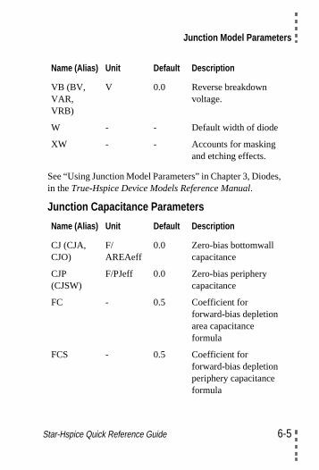
s,
See “Using Junction Model Parameters” in Chapter 3, Diodein theTrue-Hspice Device Models Reference Manual.Junction Capacitance Parameters
VB (BV,VAR,VRB)
V 0.0 Reverse breakdownvoltage.
W - - Default width of diode
XW - - Accounts for maskingand etching effects.
Name (Alias) Unit Default Description
CJ (CJA,CJO)
F/AREAeff
0.0 Zero-bias bottomwallcapacitance
CJP(CJSW)
F/PJeff 0.0 Zero-bias peripherycapacitance
FC - 0.5 Coefficient forforward-bias depletionarea capacitanceformula
FCS - 0.5 Coefficient forforward-bias depletionperiphery capacitanceformula
Name (Alias) Unit Default Description
Star-Hspice Quick Reference Guide 6-5
Diodes
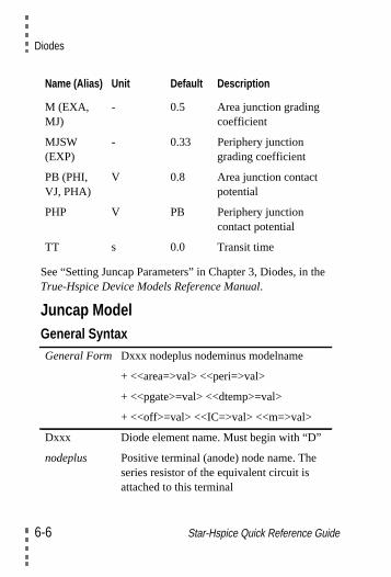
he
See “Setting Juncap Parameters” in Chapter 3, Diodes, in tTrue-Hspice Device Models Reference Manual.Juncap ModelGeneral Syntax
M (EXA,MJ)
- 0.5 Area junction gradingcoefficient
MJSW(EXP)
- 0.33 Periphery junctiongrading coefficient
PB (PHI,VJ, PHA)
V 0.8 Area junction contactpotential
PHP V PB Periphery junctioncontact potential
TT s 0.0 Transit time
General Form Dxxx nodeplus nodeminus modelname
+ <<area=>val> <<peri=>val>
+ <<pgate>=val> <<dtemp>=val>
+ <<off>=val> <<IC=>val> <<m=>val>
Dxxx Diode element name. Must begin with “D”
nodeplus Positive terminal (anode) node name. Theseries resistor of the equivalent circuit isattached to this terminal
Name (Alias) Unit Default Description
6-6 Star-Hspice Quick Reference Guide

Juncap Model
d
nminus Negative terminal (cathode) node name
mname Diode model name reference
area Diode area. In the model card, it can be useby AB
peri Length of the side-wall of the diffusion areaAB which is not under the gate. In themodel card, it is used by LS
pgate Length of the side-wall of the diffusion areaAB which is under the gate. In the modelcard, it is used by LG
off Sets initial condition to OFF for thiselement in DC analysis. The default is ON
M Multiplier to simulate multiple diodes inparallel. All currents, capacitances andresistances are affected by setting M.Default=1
ic Initial voltage across the diode element.This value is used when the UIC option ispresent in the .tran statement and isoverridden by the .ic statement
Dtemp The difference between the elementtemperature and circuit temperature incelsius. Default=0.0
.option list Prints the updated temperature parametersfor juncap diode model
Star-Hspice Quick Reference Guide 6-7
Diodes
Juncap Model Statement
See “Using the Juncap Model” in Chapter 3, Diodes, in theTrue-Hspice Device Models Reference Manual.
Juncap Model Parameters
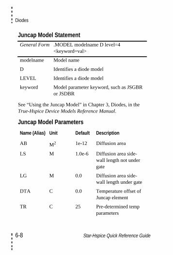
General Form .MODEL modelname D level=4<keyword=val>
modelname Model name
D Identifies a diode model
LEVEL Identifies a diode model
keyword Model parameter keyword, such as JSGBRor JSDBR
Name (Alias) Unit Default Description
AB M2 1e-12 Diffusion area
LS M 1.0e-6 Diffusion area side-wall length not undergate
LG M 0.0 Diffusion area side-wall length under gate
DTA C 0.0 Temperature offset ofJuncap element
TR C 25 Pre-determined tempparameters
6-8 Star-Hspice Quick Reference Guide
Juncap Model
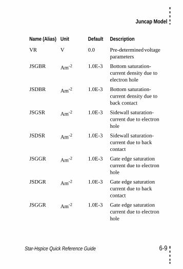
VR V 0.0 Pre-determinedvoltageparameters
JSGBR Am-2 1.0E-3 Bottom saturation-current density due toelectron hole
JSDBR Am-2 1.0E-3 Bottom saturation-current density due toback contact
JSGSR Am-2 1.0E-3 Sidewall saturation-current due to electronhole
JSDSR Am-2 1.0E-3 Sidewall saturation-current due to backcontact
JSGGR Am-2 1.0E-3 Gate edge saturationcurrent due to electronhole
JSDGR Am-2 1.0E-3 Gate edge saturationcurrent due to backcontact
JSGGR Am-2 1.0E-3 Gate edge saturationcurrent due to electronhole
Name (Alias) Unit Default Description
Star-Hspice Quick Reference Guide 6-9
Diodes
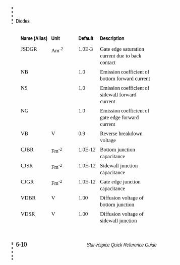
JSDGR Am-2 1.0E-3 Gate edge saturationcurrent due to backcontact
NB 1.0 Emission coefficient ofbottom forward current
NS 1.0 Emission coefficient ofsidewall forwardcurrent
NG 1.0 Emission coefficient ofgate edge forwardcurrent
VB V 0.9 Reverse breakdownvoltage
CJBR Fm-2 1.0E-12 Bottom junctioncapacitance
CJSR Fm-2 1.0E-12 Sidewall junctioncapacitance
CJGR Fm-2 1.0E-12 Gate edge junctioncapacitance
VDBR V 1.00 Diffusion voltage ofbottom junction
VDSR V 1.00 Diffusion voltage ofsidewall junction
Name (Alias) Unit Default Description
6-10 Star-Hspice Quick Reference Guide
Juncap Model
e
See “Juncap Model Parameters” in Chapter 3, Diodes, in thTrue-Hspice Device Models Reference Manual.Metal and Poly Parameters Level 3
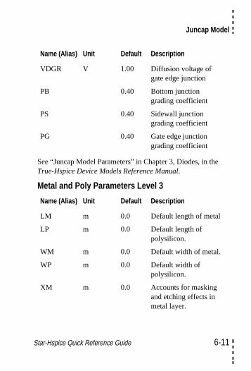
VDGR V 1.00 Diffusion voltage ofgate edge junction
PB 0.40 Bottom junctiongrading coefficient
PS 0.40 Sidewall junctiongrading coefficient
PG 0.40 Gate edge junctiongrading coefficient
Name (Alias) Unit Default Description
LM m 0.0 Default length of metal
LP m 0.0 Default length ofpolysilicon.
WM m 0.0 Default width of metal.
WP m 0.0 Default width ofpolysilicon.
XM m 0.0 Accounts for maskingand etching effects inmetal layer.
Name (Alias) Unit Default Description
Star-Hspice Quick Reference Guide 6-11
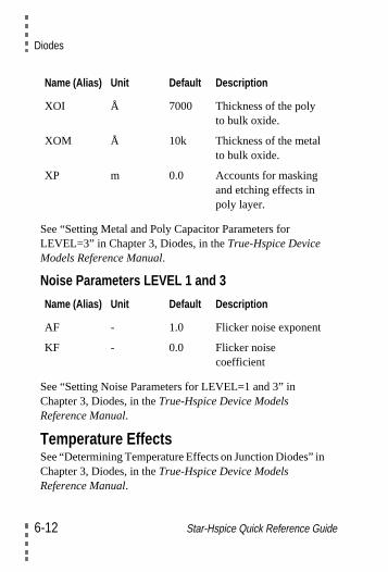
Diodes
n
See “Setting Metal and Poly Capacitor Parameters forLEVEL=3” in Chapter 3, Diodes, in theTrue-Hspice DeviceModels Reference Manual.
Noise Parameters LEVEL 1 and 3
See “Setting Noise Parameters for LEVEL=1 and 3” inChapter 3, Diodes, in theTrue-Hspice Device ModelsReference Manual.
Temperature EffectsSee “Determining Temperature Effects on Junction Diodes” iChapter 3, Diodes, in theTrue-Hspice Device ModelsReference Manual.
XOI Å 7000 Thickness of the polyto bulk oxide.
XOM Å 10k Thickness of the metalto bulk oxide.
XP m 0.0 Accounts for maskingand etching effects inpoly layer.
Name (Alias) Unit Default Description
AF - 1.0 Flicker noise exponent
KF - 0.0 Flicker noisecoefficient
Name (Alias) Unit Default Description
6-12 Star-Hspice Quick Reference Guide
Temperature Effects
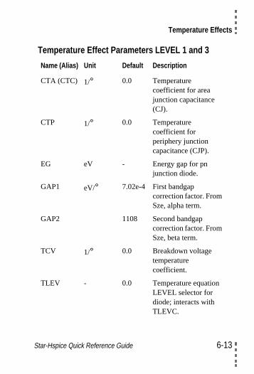
Temperature Effect Parameters LEVEL 1 and 3
Name (Alias) Unit Default Description
CTA (CTC) 1/° 0.0 Temperaturecoefficient for areajunction capacitance(CJ).
CTP 1/° 0.0 Temperaturecoefficient forperiphery junctioncapacitance (CJP).
EG eV - Energy gap for pnjunction diode.
GAP1 eV/° 7.02e-4 First bandgapcorrection factor. FromSze, alpha term.
GAP2 1108 Second bandgapcorrection factor. FromSze, beta term.
TCV 1/° 0.0 Breakdown voltagetemperaturecoefficient.
TLEV - 0.0 Temperature equationLEVEL selector fordiode; interacts withTLEVC.
Star-Hspice Quick Reference Guide 6-13
Diodes
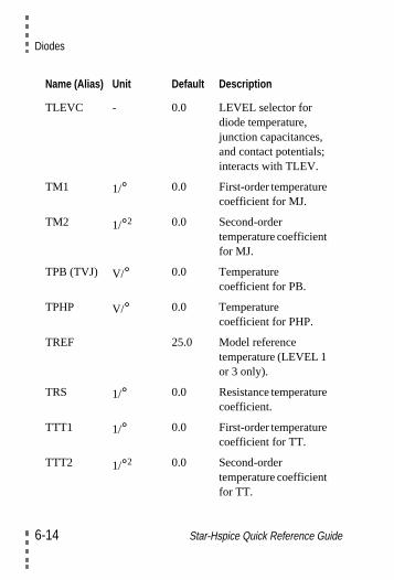
TLEVC - 0.0 LEVEL selector fordiode temperature,junction capacitances,and contact potentials;interacts with TLEV.
TM1 1/° 0.0 First-order temperaturecoefficient for MJ.
TM2 1/°2 0.0 Second-ordertemperature coefficientfor MJ.
TPB (TVJ) V/° 0.0 Temperaturecoefficient for PB.
TPHP V/° 0.0 Temperaturecoefficient for PHP.
TREF 25.0 Model referencetemperature (LEVEL 1or 3 only).
TRS 1/° 0.0 Resistance temperaturecoefficient.
TTT1 1/° 0.0 First-order temperaturecoefficient for TT.
TTT2 1/°2 0.0 Second-ordertemperature coefficientfor TT.
Name (Alias) Unit Default Description
6-14 Star-Hspice Quick Reference Guide
Fowler-Nordheim Diode
”
l
See “Setting Temperature Effect Parameters LEVEL=1 and 3in Chapter 3, Diodes, in theTrue-Hspice Device ModelsReference Manual.
Fowler-Nordheim DiodeSee “Using the Fowler-Nordheim Diode” in Chapter 3,Diodes, in theTrue-Hspice Device Models Reference Manua.
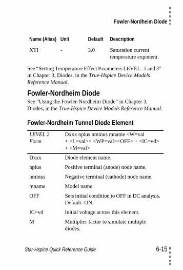
Fowler-Nordheim Tunnel Diode Element
XTI - 3.0 Saturation currenttemperature exponent.
LEVEL 2Form
Dxxx nplus nminus mname <W=val+ <L=val>> <WP=val><OFF> + <IC=vd>+ <M=val>
Dxxx Diode element name.
nplus Positive terminal (anode) node name.
nminus Negative terminal (cathode) node name.
mname Model name.
OFF Sets initial condition to OFF in DC analysis.Default=ON.
IC=vd Initial voltage across this element.
M Multiplier factor to simulate multiplediodes.
Name (Alias) Unit Default Description
Star-Hspice Quick Reference Guide 6-15
Diodes
See “Diode Element” in Chapter 3, Diodes, in theTrue-HspiceDevice Models Reference Manual.
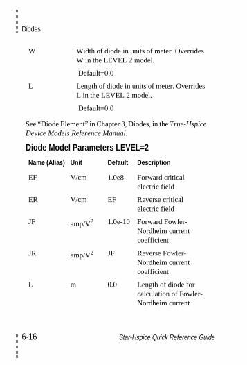
Diode Model Parameters LEVEL=2
W Width of diode in units of meter. OverridesW in the LEVEL 2 model.
Default=0.0
L Length of diode in units of meter. OverridesL in the LEVEL 2 model.
Default=0.0
Name (Alias) Unit Default Description
EF V/cm 1.0e8 Forward criticalelectric field
ER V/cm EF Reverse criticalelectric field
JF amp/V2 1.0e-10 Forward Fowler-Nordheim currentcoefficient
JR amp/V2 JF Reverse Fowler-Nordheim currentcoefficient
L m 0.0 Length of diode forcalculation of Fowler-Nordheim current
6-16 Star-Hspice Quick Reference Guide
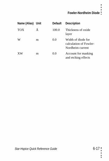
Fowler-Nordheim Diode
TOX Å 100.0 Thickness of oxidelayer
W m 0.0 Width of diode forcalculation of Fowler-Nordheim current
XW m 0.0 Account for maskingand etching effects
Name (Alias) Unit Default Description
Star-Hspice Quick Reference Guide 6-17
Diodes
6-18 Star-Hspice Quick Reference Guide
Star-Hspice Quic
7-
Chapter 7BJT Element
The topics covered in this chapter are:
• Bipolar Junction Transistors (BJTs) Element
• BJT Model Statement
• BJT Model Parameters
• LEVEL 6 Philips Bipolar Model-503 and 504
• LEVEL 8 HiCUM Model
• Level 9 VBIC99 Model
• Level 10 MODELLA Model
• Level 11 UCSD HBT Model
k Reference Guide 7-1
BJT Element
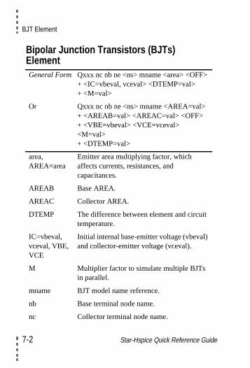
Bipolar Junction Transistors (BJTs)ElementGeneral Form Qxxx nc nb ne <ns> mname <area> <OFF>
+ <IC=vbeval, vceval> <DTEMP=val>+ <M=val>
Or Qxxx nc nb ne <ns> mname <AREA=val>+ <AREAB=val> <AREAC=val> <OFF>+ <VBE=vbeval> <VCE=vceval><M=val>+ <DTEMP=val>
area,AREA=area
Emitter area multiplying factor, whichaffects currents, resistances, andcapacitances.
AREAB Base AREA.
AREAC Collector AREA.
DTEMP The difference between element and circuittemperature.
IC=vbeval,vceval, VBE,VCE
Initial internal base-emitter voltage (vbeval)and collector-emitter voltage (vceval).
M Multiplier factor to simulate multiple BJTsin parallel.
mname BJT model name reference.
nb Base terminal node name.
nc Collector terminal node name.
7-2 Star-Hspice Quick Reference Guide
BJT Model Statement
See“Bipolar Junction Transistors (BJTs) Element” in theStar-Hspice Manual.
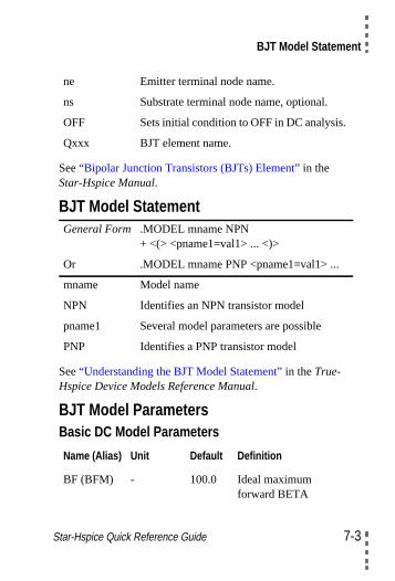
BJT Model Statement
See“Understanding the BJT Model Statement” in theTrue-Hspice Device Models Reference Manual.
BJT Model ParametersBasic DC Model Parameters
ne Emitter terminal node name.
ns Substrate terminal node name, optional.
OFF Sets initial condition to OFF in DC analysis.
Qxxx BJT element name.
General Form .MODEL mname NPN+ <(> <pname1=val1> ... <)>
Or .MODEL mname PNP <pname1=val1> ...
mname Model name
NPN Identifies an NPN transistor model
pname1 Several model parameters are possible
PNP Identifies a PNP transistor model
Name (Alias) Unit Default Definition
BF (BFM) - 100.0 Ideal maximumforward BETA
Star-Hspice Quick Reference Guide 7-3
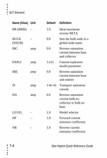
BJT Element
BR (BRM) - 1.0 Ideal maximumreverse BETA
BULK(NSUB)
- 0.0 Sets the bulk node to aglobal node name
IBC amp 0.0 Reverse saturationcurrent between baseand collector
EXPLI amp 1.e15 Current explosionmodel parameter
IBE amp 0.0 Reverse saturationcurrent between baseand emitter
IS amp 1.0e-16 Transport saturationcurrent
ISS amp 0.0 Reverse saturationcurrent bulk-to-collector or bulk-to-base
LEVEL - 1.0 Model selector
NF - 1.0 Forward currentemission coefficient
NR - 1.0 Reverse currentemission coefficient
Name (Alias) Unit Default Definition
7-4 Star-Hspice Quick Reference Guide
BJT Model Parameters
”
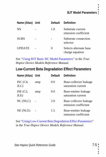
See“Using BJT Basic DC Model Parameters” in theTrue-Hspice Device Models Reference Manual.
Low-Current Beta Degradation Effect Parameters
See“Using Low-Current Beta Degradation Effect Parametersin theTrue-Hspice Device Models Reference Manual.
NS - 1.0 Substrate currentemission coefficient
SUBS - - Substrate connectionselector
UPDATE - 0 Selects alternate basecharge equation
Name (Alias) Unit Default Definition
ISC (C4,JLC)
amp 0.0 Base-collector leakagesaturation current
ISE (C2,JLE)
amp 0.0 Base-emitter leakagesaturation current
NC (NLC) - 2.0 Base-collector leakageemission coefficient
NE (NLE) - 1.5 Base-emitter leakageemission coefficient
Name (Alias) Unit Default Definition
Star-Hspice Quick Reference Guide 7-5
BJT Element
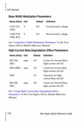
Base Width Modulation Parameters
See“Using Base Width Modulation Parameters” in theTrue-Hspice Device Models Reference Manual.
High-Current Beta Degradation Effect Parameters
See“Using High-Current Beta Degradation EffectParameters” in theTrue-Hspice Device Models ReferenceManual.
Name (Alias) Unit Default Definition
VAF (VA,VBF)
V 0.0 Forward early voltage
VAR (VB,VRB, BV)
V 0.0 Reverse early voltage
Name (Alias) Unit Default Definition
IKF (IK,JBF)
amp 0.0 Corner for forward Betahigh-current roll-off
IKR (JBR) amp 0.0 Corner for reverse Betahigh-current roll-off
NKF - 0.5 Exponent for high-current Beta roll-off
IKF (IK,JBF)
amp 0.0 Corner for forward Betahigh-current roll-off
7-6 Star-Hspice Quick Reference Guide
BJT Model Parameters
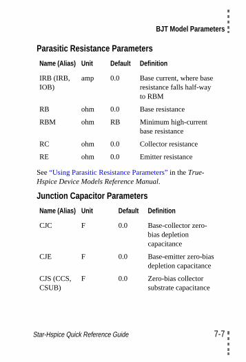
Parasitic Resistance Parameters
See“Using Parasitic Resistance Parameters” in theTrue-Hspice Device Models Reference Manual.
Junction Capacitor Parameters
Name (Alias) Unit Default Definition
IRB (IRB,IOB)
amp 0.0 Base current, where baseresistance falls half-wayto RBM
RB ohm 0.0 Base resistance
RBM ohm RB Minimum high-currentbase resistance
RC ohm 0.0 Collector resistance
RE ohm 0.0 Emitter resistance
Name (Alias) Unit Default Definition
CJC F 0.0 Base-collector zero-bias depletioncapacitance
CJE F 0.0 Base-emitter zero-biasdepletion capacitance
CJS (CCS,CSUB)
F 0.0 Zero-bias collectorsubstrate capacitance
Star-Hspice Quick Reference Guide 7-7
BJT Element
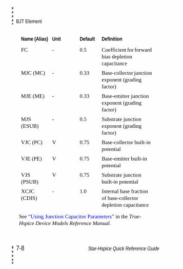
See“Using Junction Capacitor Parameters” in theTrue-Hspice Device Models Reference Manual.
FC - 0.5 Coefficient for forwardbias depletioncapacitance
MJC (MC) - 0.33 Base-collector junctionexponent (gradingfactor)
MJE (ME) - 0.33 Base-emitter junctionexponent (gradingfactor)
MJS(ESUB)
- 0.5 Substrate junctionexponent (gradingfactor)
VJC (PC) V 0.75 Base-collector built-inpotential
VJE (PE) V 0.75 Base-emitter built-inpotential
VJS(PSUB)
V 0.75 Substrate junctionbuilt-in potential
XCJC(CDIS)
- 1.0 Internal base fractionof base-collectordepletion capacitance
Name (Alias) Unit Default Definition
7-8 Star-Hspice Quick Reference Guide
BJT Model Parameters
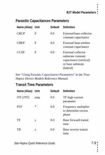
Parasitic Capacitances Parameters
See“Using Parasitic Capacitances Parameters” in theTrue-Hspice Device Models Reference Manual.
Transit Time Parameters
Name (Alias) Unit Default Definition
CBCP F 0.0 External base-collectorconstant capacitance
CBEP F 0.0 External base-emitterconstant capacitance
CCSP F 0.0 External collectorsubstrate constantcapacitance (vertical)or base substrate(lateral)
Name (Alias) Unit Default Definition
ITF (JTF) amp 0.0 TF high-currentparameter
PTF ° 0.0 Frequency multiplierto determine excessphase
TF s 0.0 Base forward transittime
TR s 0.0 Base reverse transittime
Star-Hspice Quick Reference Guide 7-9
BJT Element
See“Using Transit Time Parameters” in theTrue-HspiceDevice Models Reference Manual.
Noise Parameters
See“Using Noise Parameters” in theTrue-Hspice DeviceModels Reference Manual.
LEVEL 6 Philips Bipolar Model
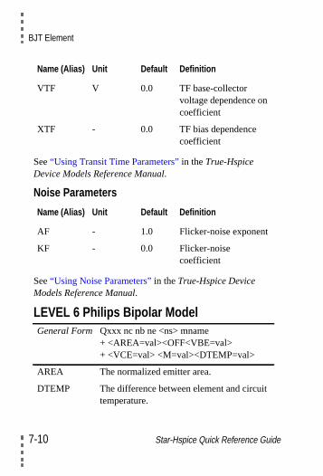
VTF V 0.0 TF base-collectorvoltage dependence oncoefficient
XTF - 0.0 TF bias dependencecoefficient
Name (Alias) Unit Default Definition
AF - 1.0 Flicker-noise exponent
KF - 0.0 Flicker-noisecoefficient
General Form Qxxx nc nb ne <ns> mname+ <AREA=val><OFF<VBE=val>+ <VCE=val> <M=val><DTEMP=val>
AREA The normalized emitter area.
DTEMP The difference between element and circuittemperature.
Name (Alias) Unit Default Definition
7-10 Star-Hspice Quick Reference Guide

LEVEL 6 Philips Bipolar Model
,e
e
See“LEVEL 6 Element Syntax” in theTrue-Hspice DeviceModels Reference Manual.
LEVEL 6 Model ParametersThe following tables describe MEXTRAM as LEVEL 6 modelparameters including parameters name, descriptions, unitsdefault values and notes. For more detailed information, se“LEVEL 6 Model Parameters” in theTrue-Hspice DeviceModels Reference Manual.
This section describes parameters for LEVEL 503 only. Sethe following section free-fell 6 Philips Bipolar Model(MEXTRAM LEVEL 504)” parameters.
M Multiplier to simulate multiple BJTs inparallel.
mname BJT model name reference.
nb Base node name or number.
nc Collector terminal node name or number.
ne Emitter terminal node name or number.
ns Substrate node name or number.
OFF Sets initial condition to OFF for thiselement in DC analysis.
Qxxx BJT element name.
VBE Initial internal base to emitter voltage.
VCE Initial internal collector to emitter voltage.
Star-Hspice Quick Reference Guide 7-11
BJT Element
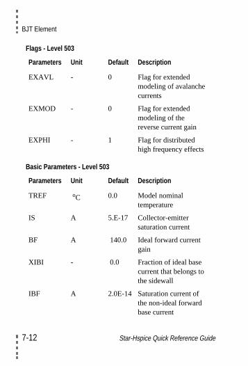
Flags - Level 503
Basic Parameters - Level 503
Parameters Unit Default Description
EXAVL - 0 Flag for extendedmodeling of avalanchecurrents
EXMOD - 0 Flag for extendedmodeling of thereverse current gain
EXPHI - 1 Flag for distributedhigh frequency effects
Parameters Unit Default Description
TREF oC 0.0 Model nominaltemperature
IS A 5.E-17 Collector-emittersaturation current
BF A 140.0 Ideal forward currentgain
XIBI - 0.0 Fraction of ideal basecurrent that belongs tothe sidewall
IBF A 2.0E-14 Saturation current ofthe non-ideal forwardbase current
7-12 Star-Hspice Quick Reference Guide
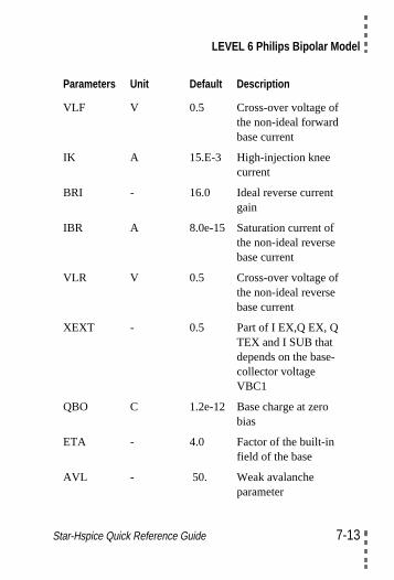
LEVEL 6 Philips Bipolar Model
VLF V 0.5 Cross-over voltage ofthe non-ideal forwardbase current
IK A 15.E-3 High-injection kneecurrent
BRI - 16.0 Ideal reverse currentgain
IBR A 8.0e-15 Saturation current ofthe non-ideal reversebase current
VLR V 0.5 Cross-over voltage ofthe non-ideal reversebase current
XEXT - 0.5 Part of I EX,Q EX, QTEX and I SUB thatdepends on the base-collector voltageVBC1
QBO C 1.2e-12 Base charge at zerobias
ETA - 4.0 Factor of the built-infield of the base
AVL - 50. Weak avalancheparameter
Parameters Unit Default Description
Star-Hspice Quick Reference Guide 7-13
BJT Element
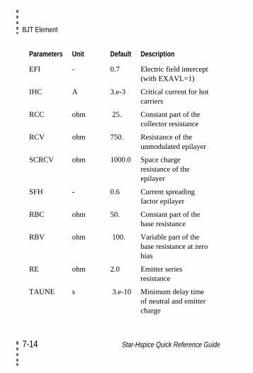
EFI - 0.7 Electric field intercept(with EXAVL=1)
IHC A 3.e-3 Critical current for hotcarriers
RCC ohm 25. Constant part of thecollector resistance
RCV ohm 750. Resistance of theunmodulated epilayer
SCRCV ohm 1000.0 Space chargeresistance of theepilayer
SFH - 0.6 Current spreadingfactor epilayer
RBC ohm 50. Constant part of thebase resistance
RBV ohm 100. Variable part of thebase resistance at zerobias
RE ohm 2.0 Emitter seriesresistance
TAUNE s 3.e-10 Minimum delay timeof neutral and emittercharge
Parameters Unit Default Description
7-14 Star-Hspice Quick Reference Guide
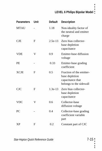
LEVEL 6 Philips Bipolar Model
MTAU - 1.18 Non-ideality factor ofthe neutral and emittercharge
CJE F 2.5e-13 Zero bias collector-base depletioncapacitance
VDE V 0.9 Emitter-base diffusionvoltage
PE - 0.33 Emitter-base gradingcoefficient
XCJE F 0.5 Fraction of the emitter-base depletioncapacitance thatbelongs to the sidewall
CJC F 1.3e-13 Zero bias collector-base depletioncapacitance
VDC V 0.6 Collector-basediffusion voltage
PC - 0.4 Collector-base gradingcoefficient variablepart
XP F 0.2 Constant part of CJC
Parameters Unit Default Description
Star-Hspice Quick Reference Guide 7-15
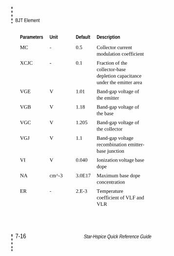
BJT Element
MC - 0.5 Collector currentmodulation coefficient
XCJC - 0.1 Fraction of thecollector-basedepletion capacitanceunder the emitter area
VGE V 1.01 Band-gap voltage ofthe emitter
VGB V 1.18 Band-gap voltage ofthe base
VGC V 1.205 Band-gap voltage ofthe collector
VGJ V 1.1 Band-gap voltagerecombination emitter-base junction
VI V 0.040 Ionization voltage basedope
NA cm^-3 3.0E17 Maximum base dopeconcentration
ER - 2.E-3 Temperaturecoefficient of VLF andVLR
Parameters Unit Default Description
7-16 Star-Hspice Quick Reference Guide
LEVEL 6 Philips Bipolar Model
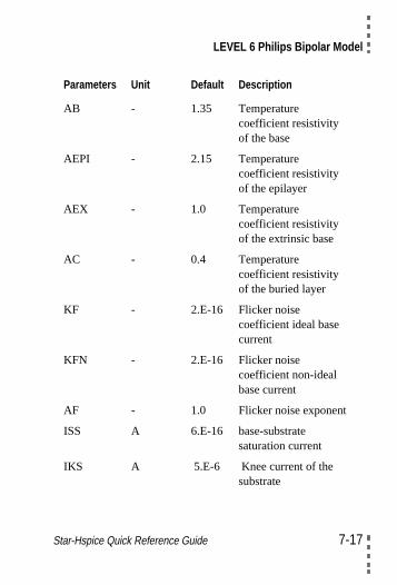
Star-Hspice Quick Reference Guide 7-17
AB - 1.35 Temperaturecoefficient resistivityof the base
AEPI - 2.15 Temperaturecoefficient resistivityof the epilayer
AEX - 1.0 Temperaturecoefficient resistivityof the extrinsic base
AC - 0.4 Temperaturecoefficient resistivityof the buried layer
KF - 2.E-16 Flicker noisecoefficient ideal basecurrent
KFN - 2.E-16 Flicker noisecoefficient non-idealbase current
AF - 1.0 Flicker noise exponent
ISS A 6.E-16 base-substratesaturation current
IKS A 5.E-6 Knee current of thesubstrate
Parameters Unit Default Description
BJT Element
t,
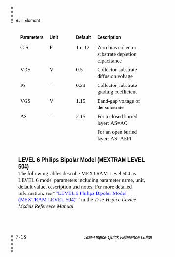
LEVEL 6 Philips Bipolar Model (MEXTRAM LEVEL504)The following tables describe MEXTRAM Level 504 asLEVEL 6 model parameters including parameter name, unidefault value, description and notes. For more detailedinformation, see ““LEVEL 6 Philips Bipolar Model(MEXTRAM LEVEL 504)”” in theTrue-Hspice DeviceModels Reference Manual.
CJS F 1.e-12 Zero bias collector-substrate depletioncapacitance
VDS V 0.5 Collector-substratediffusion voltage
PS - 0.33 Collector-substrategrading coefficient
VGS V 1.15 Band-gap voltage ofthe substrate
AS - 2.15 For a closed buriedlayer: AS=AC
For an open buriedlayer: AS=AEPI
Parameters Unit Default Description
7-18 Star-Hspice Quick Reference Guide
LEVEL 6 Philips Bipolar Model
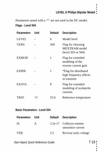
Parameters noted with a ‘*’ are not used in the DC model.
Flags - Level 504
Parameters Unit Default Description
LEVEL - 6 Model level
VERS - 504 Flag for choosingMEXTRAM model(level 503 or 504)
EXMOD - 1 Flag for extendedmodeling of thereverse current gain
EXPHI - 1 *Flag for distributedhigh frequency effectsin transient
EXAVL - 0 Flag for extendedmodeling of avalanchecurrents
TREF ^C 25.0 Reference temperature
Basic Parameters - Level 504
Parameters Unit Default Description
IS A 2.2e-17 Collector-emittersaturation current
VER 2.5 Reverse early voltage
Star-Hspice Quick Reference Guide 7-19
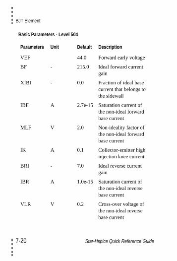
BJT Element
VEF 44.0 Forward early voltage
BF - 215.0 Ideal forward currentgain
XIBI - 0.0 Fraction of ideal basecurrent that belongs tothe sidewall
IBF A 2.7e-15 Saturation current ofthe non-ideal forwardbase current
MLF V 2.0 Non-ideality factor ofthe non-ideal forwardbase current
IK A 0.1 Collector-emitter highinjection knee current
BRI - 7.0 Ideal reverse currentgain
IBR A 1.0e-15 Saturation current ofthe non-ideal reversebase current
VLR V 0.2 Cross-over voltage ofthe non-ideal reversebase current
Basic Parameters - Level 504
Parameters Unit Default Description
7-20 Star-Hspice Quick Reference Guide
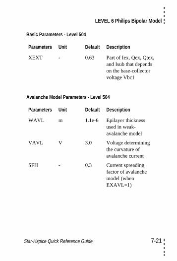
LEVEL 6 Philips Bipolar Model
XEXT - 0.63 Part of Iex, Qex, Qtex,and Isub that dependson the base-collectorvoltage Vbc1
Avalanche Model Parameters - Level 504
Parameters Unit Default Description
WAVL m 1.1e-6 Epilayer thicknessused in weak-avalanche model
VAVL V 3.0 Voltage determiningthe curvature ofavalanche current
SFH - 0.3 Current spreadingfactor of avalanchemodel (whenEXAVL=1)
Basic Parameters - Level 504
Parameters Unit Default Description
Star-Hspice Quick Reference Guide 7-21
BJT Element
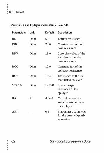
Resistance and Epilayer Parameters - Level 504
Parameters Unit Default Description
RE Ohm 5.0 Emitter resistance
RBC Ohm 23.0 Constant part of thebase resistance
RBV Ohm 18.0 Zero-bias value of thevariable part of thebase resistance
RCC Ohm 12.0 Constant part of thecollector resistance
RCV Ohm 150.0 Resistance of the un-modulated epilayer
SCRCV Ohm 1250.0 Space chargeresistance of theepilayer
IHC A 4.0e-3 Critical current forvelocity saturation inthe epilayer
AXI - 0.3 Smoothness parameterfor the onset of quasi-saturation
7-22 Star-Hspice Quick Reference Guide
LEVEL 6 Philips Bipolar Model
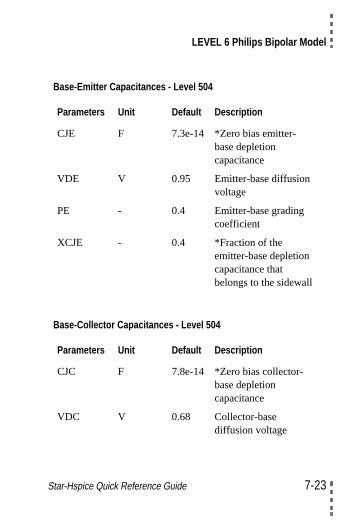
Base-Emitter Capacitances - Level 504
Parameters Unit Default Description
CJE F 7.3e-14 *Zero bias emitter-base depletioncapacitance
VDE V 0.95 Emitter-base diffusionvoltage
PE - 0.4 Emitter-base gradingcoefficient
XCJE - 0.4 *Fraction of theemitter-base depletioncapacitance thatbelongs to the sidewall
Base-Collector Capacitances - Level 504
Parameters Unit Default Description
CJC F 7.8e-14 *Zero bias collector-base depletioncapacitance
VDC V 0.68 Collector-basediffusion voltage
Star-Hspice Quick Reference Guide 7-23
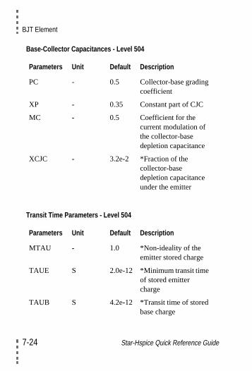
BJT Element
PC - 0.5 Collector-base gradingcoefficient
XP - 0.35 Constant part of CJC
MC - 0.5 Coefficient for thecurrent modulation ofthe collector-basedepletion capacitance
XCJC - 3.2e-2 *Fraction of thecollector-basedepletion capacitanceunder the emitter
Transit Time Parameters - Level 504
Parameters Unit Default Description
MTAU - 1.0 *Non-ideality of theemitter stored charge
TAUE S 2.0e-12 *Minimum transit timeof stored emittercharge
TAUB S 4.2e-12 *Transit time of storedbase charge
Base-Collector Capacitances - Level 504
Parameters Unit Default Description
7-24 Star-Hspice Quick Reference Guide
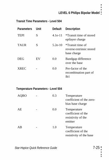
LEVEL 6 Philips Bipolar Model
TEPI S 4.1e-11 *Transit time of storedepilayer charge
TAUR S 5.2e-10 *Transit time ofreverse extrinsic storedbase charge
DEG EV 0.0 Bandgap differenceover the base
XREC - 0.0 Pre-factor of therecombination part ofIb1
Temperature Parameters - Level 504
AQBO - 0.3 Temperaturecoefficient of the zero-bias base charge
AE - 0.0 Temperaturecoefficient of theresistivity of theemitter
AB - 1.0 Temperaturecoefficient of theresistivity of the base
Transit Time Parameters - Level 504
Parameters Unit Default Description
Star-Hspice Quick Reference Guide 7-25
BJT Element
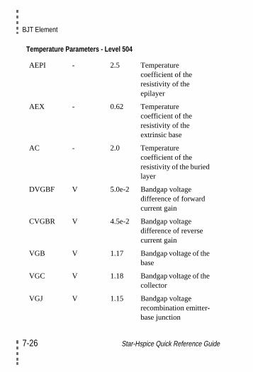
AEPI - 2.5 Temperaturecoefficient of theresistivity of theepilayer
AEX - 0.62 Temperaturecoefficient of theresistivity of theextrinsic base
AC - 2.0 Temperaturecoefficient of theresistivity of the buriedlayer
DVGBF V 5.0e-2 Bandgap voltagedifference of forwardcurrent gain
CVGBR V 4.5e-2 Bandgap voltagedifference of reversecurrent gain
VGB V 1.17 Bandgap voltage of thebase
VGC V 1.18 Bandgap voltage of thecollector
VGJ V 1.15 Bandgap voltagerecombination emitter-base junction
Temperature Parameters - Level 504
7-26 Star-Hspice Quick Reference Guide
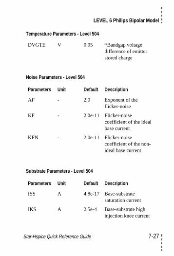
LEVEL 6 Philips Bipolar Model
Star-Hspice Quick Reference Guide 7-27
DVGTE V 0.05 *Bandgap voltagedifference of emitterstored charge
Noise Parameters - Level 504
Parameters Unit Default Description
AF - 2.0 Exponent of theflicker-noise
KF - 2.0e-11 Flicker-noisecoefficient of the idealbase current
KFN - 2.0e-11 Flicker-noisecoefficient of the non-ideal base current
Substrate Parameters - Level 504
Parameters Unit Default Description
ISS A 4.8e-17 Base-substratesaturation current
IKS A 2.5e-4 Base-substrate highinjection knee current
Temperature Parameters - Level 504
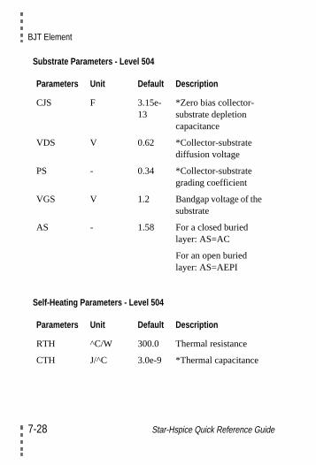
BJT Element
CJS F 3.15e-13
*Zero bias collector-substrate depletioncapacitance
VDS V 0.62 *Collector-substratediffusion voltage
PS - 0.34 *Collector-substrategrading coefficient
VGS V 1.2 Bandgap voltage of thesubstrate
AS - 1.58 For a closed buriedlayer: AS=AC
For an open buriedlayer: AS=AEPI
Self-Heating Parameters - Level 504
Parameters Unit Default Description
RTH ^C/W 300.0 Thermal resistance
CTH J/^C 3.0e-9 *Thermal capacitance
Substrate Parameters - Level 504
Parameters Unit Default Description
7-28 Star-Hspice Quick Reference Guide

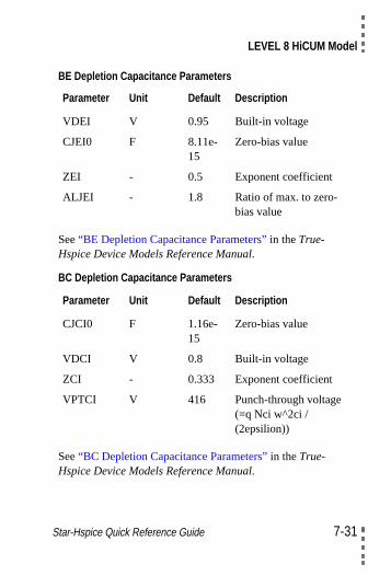
LEVEL 8 HiCUM Model
LEVEL 8 HiCUM ModelSee“LEVEL 8 HiCUM Model” in theTrue-Hspice DeviceModels Reference Manual.
Model Parameters
See“Model Parameters” in theTrue-Hspice Device ModelsReference Manual.
Parameter Unit Default Description
LEVEL - 8 HiCUM BJT LEVELin Hspice
TREF C 26.85 Temperature insimulation
Star-Hspice Quick Reference Guide 7-29
BJT Element
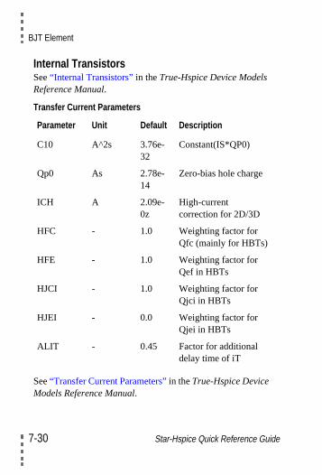
Internal TransistorsSee“Internal Transistors” in theTrue-Hspice Device ModelsReference Manual.
Transfer Current Parameters
See“Transfer Current Parameters”in theTrue-Hspice DeviceModels Reference Manual.
Parameter Unit Default Description
C10 A^2s 3.76e-32
Constant(IS*QP0)
Qp0 As 2.78e-14
Zero-bias hole charge
ICH A 2.09e-0z
High-currentcorrection for 2D/3D
HFC - 1.0 Weighting factor forQfc (mainly for HBTs)
HFE - 1.0 Weighting factor forQef in HBTs
HJCI - 1.0 Weighting factor forQjci in HBTs
HJEI - 0.0 Weighting factor forQjei in HBTs
ALIT - 0.45 Factor for additionaldelay time of iT
7-30 Star-Hspice Quick Reference Guide
LEVEL 8 HiCUM Model
BE Depletion Capacitance Parameters
See“BE Depletion Capacitance Parameters” in theTrue-Hspice Device Models Reference Manual.
BC Depletion Capacitance Parameters
See“BC Depletion Capacitance Parameters” in theTrue-Hspice Device Models Reference Manual.
Parameter Unit Default Description
VDEI V 0.95 Built-in voltage
CJEI0 F 8.11e-15
Zero-bias value
ZEI - 0.5 Exponent coefficient
ALJEI - 1.8 Ratio of max. to zero-bias value
Parameter Unit Default Description
CJCI0 F 1.16e-15
Zero-bias value
VDCI V 0.8 Built-in voltage
ZCI - 0.333 Exponent coefficient
VPTCI V 416 Punch-through voltage(=q Nci w^2ci /(2epsilion))
Star-Hspice Quick Reference Guide 7-31
BJT Element
t
Forward Transit Time Parameters
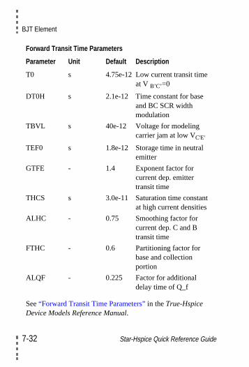
See“Forward Transit Time Parameters” in theTrue-HspiceDevice Models Reference Manual.
Parameter Unit Default Description
T0 s 4.75e-12 Low current transit timeat V B’C’ =0
DT0H s 2.1e-12 Time constant for baseand BC SCR widthmodulation
TBVL s 40e-12 Voltage for modelingcarrier jam at low VC'E'
TEF0 s 1.8e-12 Storage time in neutralemitter
GTFE - 1.4 Exponent factor forcurrent dep. emittertransit time
THCS s 3.0e-11 Saturation time constanat high current densities
ALHC - 0.75 Smoothing factor forcurrent dep. C and Btransit time
FTHC - 0.6 Partitioning factor forbase and collectionportion
ALQF - 0.225 Factor for additionaldelay time of Q_f
7-32 Star-Hspice Quick Reference Guide
LEVEL 8 HiCUM Model
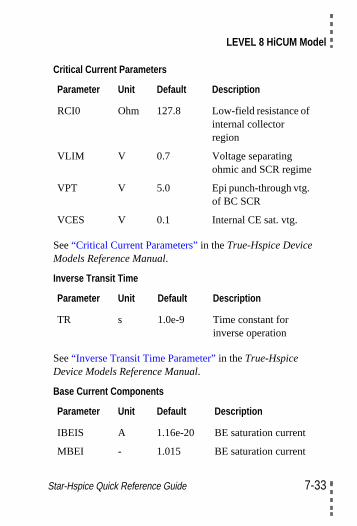
Critical Current Parameters
See“Critical Current Parameters” in theTrue-Hspice DeviceModels Reference Manual.
Inverse Transit Time
See“Inverse Transit Time Parameter” in theTrue-HspiceDevice Models Reference Manual.
Base Current Components
Parameter Unit Default Description
RCI0 Ohm 127.8 Low-field resistance ofinternal collectorregion
VLIM V 0.7 Voltage separatingohmic and SCR regime
VPT V 5.0 Epi punch-through vtg.of BC SCR
VCES V 0.1 Internal CE sat. vtg.
Parameter Unit Default Description
TR s 1.0e-9 Time constant forinverse operation
Parameter Unit Default Description
IBEIS A 1.16e-20 BE saturation current
MBEI - 1.015 BE saturation current
Star-Hspice Quick Reference Guide 7-33
BJT Element
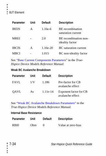
See“Base Current Components Parameters” in theTrue-Hspice Device Models Reference Manual.
Weak BC Avalanche Breakdown
See“Weak BC Avalanche Breakdown Parameters” in theTrue-Hspice Device Models Reference Manual.
Internal Base Resistance
IREIS A 1.16e-6 BE recombinationsaturation current
MREI - 2.0 BE recombination non-ideality factor
IBCIS A 1.16e-20 BC saturation current
MBCI - 1.015 BC non-ideality factor
Parameter Unit Default Description
FAVL 1/V 1.186 Pre-factor for CBavalanche effect
QAVL As 1.11e-14 Exponent factor for CBavalanche effect
Parameter Unit Default Description
RBI0 Ohm 0 Value at zero-bias
Parameter Unit Default Description
7-34 Star-Hspice Quick Reference Guide
LEVEL 8 HiCUM Model
See“Internal Base Resistance Parameters”in theTrue-HspiceDevice Models Reference Manual.
Lateral Scaling
See“Lateral Scaling” in theTrue-Hspice Device ModelsReference Manual.
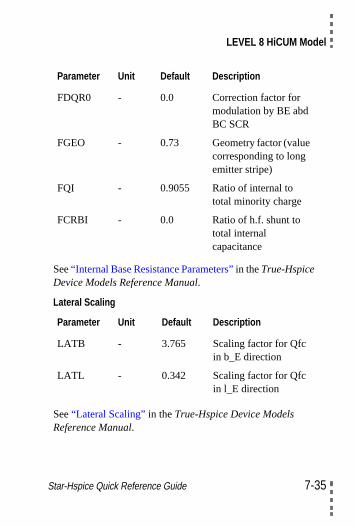
FDQR0 - 0.0 Correction factor formodulation by BE abdBC SCR
FGEO - 0.73 Geometry factor (valuecorresponding to longemitter stripe)
FQI - 0.9055 Ratio of internal tototal minority charge
FCRBI - 0.0 Ratio of h.f. shunt tototal internalcapacitance
Parameter Unit Default Description
LATB - 3.765 Scaling factor for Qfcin b_E direction
LATL - 0.342 Scaling factor for Qfcin l_E direction
Parameter Unit Default Description
Star-Hspice Quick Reference Guide 7-35
BJT Element
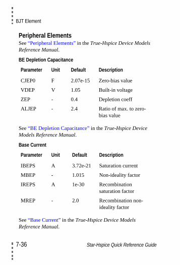
Peripheral ElementsSee“Peripheral Elements”in theTrue-Hspice Device ModelsReference Manual.
BE Depletion Capacitance
See“BE Depletion Capacitance” in theTrue-Hspice DeviceModels Reference Manual.
Base Current
See“Base Current” in theTrue-Hspice Device ModelsReference Manual.
Parameter Unit Default Description
CJEP0 F 2.07e-15 Zero-bias value
VDEP V 1.05 Built-in voltage
ZEP - 0.4 Depletion coeff
ALJEP - 2.4 Ratio of max. to zero-bias value
Parameter Unit Default Description
IBEPS A 3.72e-21 Saturation current
MBEP - 1.015 Non-ideality factor
IREPS A 1e-30 Recombinationsaturation factor
MREP - 2.0 Recombination non-ideality factor
7-36 Star-Hspice Quick Reference Guide
LEVEL 8 HiCUM Model
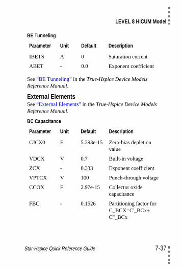
BE Tunneling
See“BE Tunneling” in theTrue-Hspice Device ModelsReference Manual.
External ElementsSee“External Elements” in theTrue-Hspice Device ModelsReference Manual.
BC Capacitance
Parameter Unit Default Description
IBETS A 0 Saturation current
ABET - 0.0 Exponent coefficient
Parameter Unit Default Description
CJCX0 F 5.393e-15 Zero-bias depletionvalue
VDCX V 0.7 Built-in voltage
ZCX - 0.333 Exponent coefficient
VPTCX V 100 Punch-through voltage
CCOX F 2.97e-15 Collector oxidecapacitance
FBC - 0.1526 Partitioning factor forC_BCX=C'_BCx+C"_BCx
Star-Hspice Quick Reference Guide 7-37
BJT Element
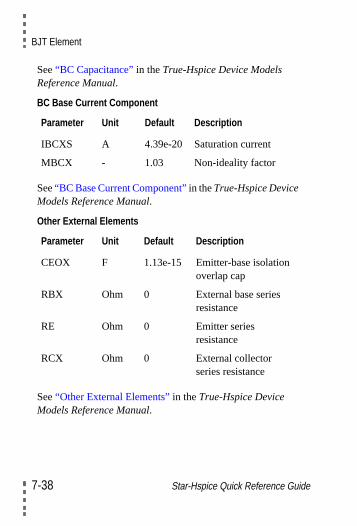
See“BC Capacitance” in theTrue-Hspice Device ModelsReference Manual.
BC Base Current Component
See“BC Base Current Component”in theTrue-Hspice DeviceModels Reference Manual.
Other External Elements
See“Other External Elements” in theTrue-Hspice DeviceModels Reference Manual.
Parameter Unit Default Description
IBCXS A 4.39e-20 Saturation current
MBCX - 1.03 Non-ideality factor
Parameter Unit Default Description
CEOX F 1.13e-15 Emitter-base isolationoverlap cap
RBX Ohm 0 External base seriesresistance
RE Ohm 0 Emitter seriesresistance
RCX Ohm 0 External collectorseries resistance
7-38 Star-Hspice Quick Reference Guide
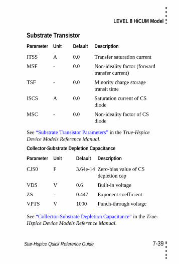
LEVEL 8 HiCUM Model
Substrate Transistor
See“Substrate Transistor Parameters” in theTrue-HspiceDevice Models Reference Manual.
Collector-Substrate Depletion Capacitance
See“Collector-Substrate Depletion Capacitance” in theTrue-Hspice Device Models Reference Manual.
Parameter Unit Default Description
ITSS A 0.0 Transfer saturation current
MSF - 0.0 Non-ideality factor (forwardtransfer current)
TSF - 0.0 Minority charge storagetransit time
ISCS A 0.0 Saturation current of CSdiode
MSC - 0.0 Non-ideality factor of CSdiode
Parameter Unit Default Description
CJS0 F 3.64e-14 Zero-bias value of CSdepletion cap
VDS V 0.6 Built-in voltage
ZS - 0.447 Exponent coefficient
VPTS V 1000 Punch-through voltage
Star-Hspice Quick Reference Guide 7-39
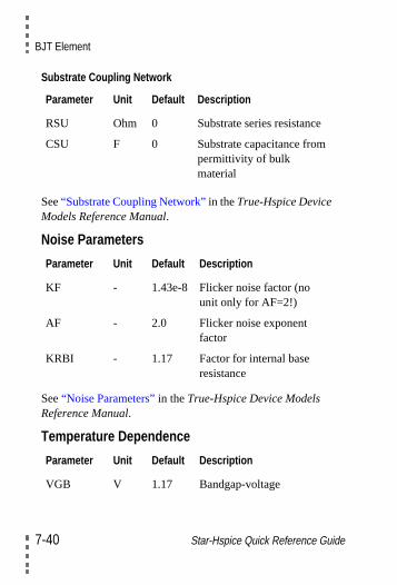
BJT Element
Substrate Coupling Network
See“Substrate Coupling Network”in theTrue-Hspice DeviceModels Reference Manual.
Noise Parameters
See“Noise Parameters” in theTrue-Hspice Device ModelsReference Manual.
Temperature Dependence
Parameter Unit Default Description
RSU Ohm 0 Substrate series resistance
CSU F 0 Substrate capacitance frompermittivity of bulkmaterial
Parameter Unit Default Description
KF - 1.43e-8 Flicker noise factor (nounit only for AF=2!)
AF - 2.0 Flicker noise exponentfactor
KRBI - 1.17 Factor for internal baseresistance
Parameter Unit Default Description
VGB V 1.17 Bandgap-voltage
7-40 Star-Hspice Quick Reference Guide
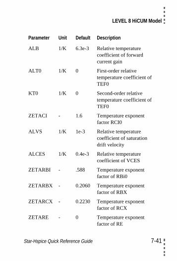
LEVEL 8 HiCUM Model
ALB 1/K 6.3e-3 Relative temperaturecoefficient of forwardcurrent gain
ALT0 1/K 0 First-order relativetemperature coefficient ofTEF0
KT0 1/K 0 Second-order relativetemperature coefficient ofTEF0
ZETACI - 1.6 Temperature exponentfactor RCI0
ALVS 1/K 1e-3 Relative temperaturecoefficient of saturationdrift velocity
ALCES 1/K 0.4e-3 Relative temperaturecoefficient of VCES
ZETARBI - .588 Temperature exponentfactor of RBi0
ZETARBX - 0.2060 Temperature exponentfactor of RBX
ZETARCX - 0.2230 Temperature exponentfactor of RCX
ZETARE - 0 Temperature exponentfactor of RE
Parameter Unit Default Description
Star-Hspice Quick Reference Guide 7-41
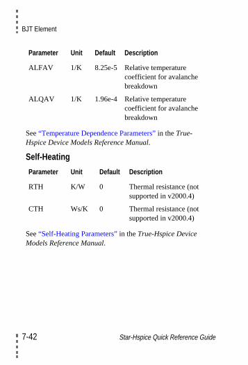
BJT Element
See“Temperature Dependence Parameters” in theTrue-Hspice Device Models Reference Manual.
Self-Heating
See“Self-Heating Parameters” in theTrue-Hspice DeviceModels Reference Manual.
ALFAV 1/K 8.25e-5 Relative temperaturecoefficient for avalanchebreakdown
ALQAV 1/K 1.96e-4 Relative temperaturecoefficient for avalanchebreakdown
Parameter Unit Default Description
RTH K/W 0 Thermal resistance (notsupported in v2000.4)
CTH Ws/K 0 Thermal resistance (notsupported in v2000.4)
Parameter Unit Default Description
7-42 Star-Hspice Quick Reference Guide
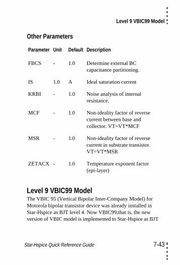
Level 9 VBIC99 Model
Other Parameters
Level 9 VBIC99 ModelThe VBIC 95 (Vertical Bipolar Inter-Company Model) forMotorola bipolar transistor device was already installed inStar-Hspice as BJT level 4. Now VBIC99,that is, the newversion of VBIC model is implemented to Star-Hspice as BJT
Parameter Unit Default Description
FBCS - 1.0 Determine external BCcapacitance partitioning.
IS 1.0 A Ideal saturation current
KRBI - 1.0 Noise analysis of internalresistance.
MCF - 1.0 Non-ideality factor of reversecurrent between base andcollector. VT=VT*MCF
MSR - 1.0 Non-ideality factor of reversecurrent in substrate transistor.VT=VT*MSR
ZETACX - 1.0 Temperature exponent factor(epi-layer)
Star-Hspice Quick Reference Guide 7-43
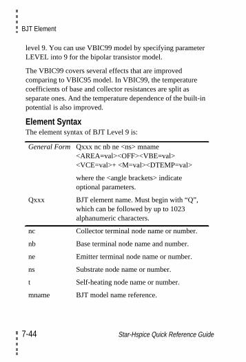
BJT Element
r
t-in
level 9. You can use VBIC99 model by specifying parameteLEVEL into 9 for the bipolar transistor model.
The VBIC99 covers several effects that are improvedcomparing to VBIC95 model. In VBIC99, the temperaturecoefficients of base and collector resistances are split asseparate ones. And the temperature dependence of the builpotential is also improved.
Element SyntaxThe element syntax of BJT Level 9 is:
General Form Qxxx nc nb ne <ns> mname<AREA=val><OFF><VBE=val><VCE=val>+ <M=val><DTEMP=val>
where the <angle brackets> indicateoptional parameters.
Qxxx BJT element name. Must begin with “Q”,which can be followed by up to 1023alphanumeric characters.
nc Collector terminal node name or number.
nb Base terminal node name and number.
ne Emitter terminal node name or number.
ns Substrate node name or number.
t Self-heating node name or number.
mname BJT model name reference.
7-44 Star-Hspice Quick Reference Guide
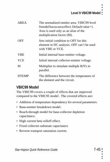
Level 9 VBIC99 Model
rs.
VBIC99 ModelThe VBIC99 covers a couple of effects that are improvedcompared to the VBIC95 model . The covered effects are:
• Addition of temperature dependency for several paramete
• Base-emitter breakdown model.
• Reach-through model for base-collector depletioncapacitance.
• High current beta rolloff effect.
• Fixed collector-substrate capacitance
• Reverse transport saturation current.
AREA The normalized emitter area. VBIC99 level9modelhasnoareaeffect.Defaultvalue=1.Area is used only as an alias of themultiplication factor (M).
OFF Sets initial condition to OFF for thiselement in DC analysis. OFF can’t be usedwith VBE or VCE.
VBE Initial internal base-emitter voltage.
VCE Initial internal collector-emitter voltage.
M Multiplier to simulate multiple BJTs inparallel.
DTEMP The difference between the temperature ofthe element and the circuit.
Star-Hspice Quick Reference Guide 7-45
BJT Element
re
n.
re
Using VBIC99 with Star-Hspice1. Set Level to 9 to identify the model as a VBIC99 bipolar
junction transistor model.
2. Reference temperature, TREF, equals to 27 degrees.
3. VBIC99 model is not supported with AREA scaling,Multiplication scaling is just supported. In HSPICE, thedefault AREA value is 1.0.
4. Self-heating is enabled for this model. Model parameters aRTH and CTH.
Level 10 MODELLA ModelThe level10 Modella model provides an extensive descriptioof a lateral integrated circuit junction-isolated PNP transistorThe equivalent circuit, analytical equations, and modelparameters are derived directly from the physics and structuof the lateral PNP. The following list summarizes the majorfeatures in level 10:
1. Current crowding under the emitter is modelled.
2. The forward early voltage is dependent on Vcb and Veb.
3. Fall off of ft and hfe is not only due to high injection but alsoto ohmic voltage drop across the emitter.
4. Separate saturation current for the substrate-base diode.
• Set LEVEL=10 to use the Level 10 Modella Model
7-46 Star-Hspice Quick Reference Guide
Level 11 UCSD HBT Model
n
elis
• The default room temperature is 25˚C in Star-Hspice. IfLEVEL 10 model parameters are specified at 27˚C,use .OPTION TNOM=27.
See“BJT Level 10 Model Parameters”in theTrue-HspiceDevice Models Reference Manual.
Level 11 UCSD HBT Model1. Most formulations from Berkeley SPICE have been
grandfathered, not all are retained.
2. The HBT model allows various degrees of trade-off betweeaccuracy and computational complexity.
3. Flags permit turning off several features of the model inorder to allow faster computation or easier convergence.
4. The default room temperature is 25oC in Star-Hspice, but is
27 oC in most other simulators.
5. The model parameter set should always include the modreference temperature TREF. The default value for TREF27.
6. DTEMP can be used with this model.
Star-Hspice Quick Reference Guide 7-47
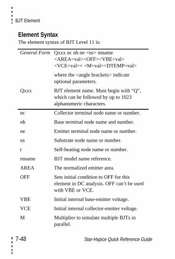
BJT Element
Element SyntaxThe element syntax of BJT Level 11 is:
General Form Qxxx nc nb ne <ns> mname<AREA=val><OFF><VBE=val><VCE=val>+ <M=val><DTEMP=val>
where the <angle brackets> indicateoptional parameters.
Qxxx BJT element name. Must begin with “Q”,which can be followed by up to 1023alphanumeric characters.
nc Collector terminal node name or number.
nb Base terminal node name and number.
ne Emitter terminal node name or number.
ns Substrate node name or number.
t Self-heating node name or number.
mname BJT model name reference.
AREA The normalized emitter area.
OFF Sets initial condition to OFF for thiselement in DC analysis. OFF can’t be usedwith VBE or VCE.
VBE Initial internal base-emitter voltage.
VCE Initial internal collector-emitter voltage.
M Multiplier to simulate multiple BJTs inparallel.
7-48 Star-Hspice Quick Reference Guide
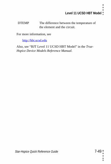
Level 11 UCSD HBT Model
For more information, see
http://hbt.ucsd.edu
Also, see “BJT Level 11 UCSD HBT Model” in theTrue-Hspice Device Models Reference Manual.
DTEMP The difference between the temperature ofthe element and the circuit.
Star-Hspice Quick Reference Guide 7-49

BJT Element
7-50 Star-Hspice Quick Reference Guide
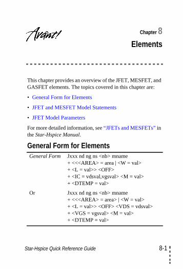
Star-Hspice Quic
8-
Chapter 8Elements
d
This chapter provides an overview of the JFET, MESFET, anGASFET elements. The topics covered in this chapter are:• General Form for Elements
• JFET and MESFET Model Statements
• JFET Model Parameters
For more detailed information, see“JFETs and MESFETs”intheStar-Hspice Manual.
General Form for ElementsGeneral Form Jxxx nd ng ns <nb> mname
+ <<<AREA> = area | <W = val>+ <L = val>> <OFF>+ <IC = vdsval,vgsval> <M = val>+ <DTEMP = val>
Or Jxxx nd ng ns <nb> mname+ <<<AREA> = area> | <W = val>+ <L = val>> <OFF> <VDS = vdsval>+ <VGS = vgsval> <M = val>+ <DTEMP = val>
k Reference Guide 8-1
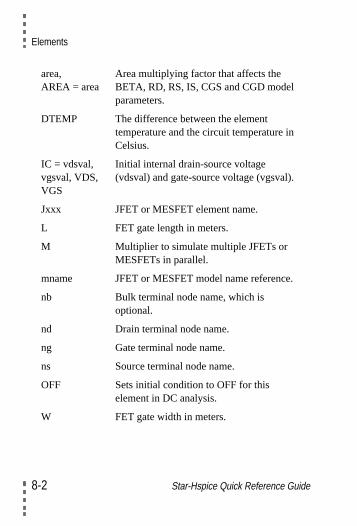
Elements
.
area,AREA = area
Area multiplying factor that affects theBETA, RD, RS, IS, CGS and CGD modelparameters.
DTEMP The difference between the elementtemperature and the circuit temperature inCelsius.
IC = vdsval,vgsval, VDS,VGS
Initial internal drain-source voltage(vdsval) and gate-source voltage (vgsval).
Jxxx JFET or MESFET element name.
L FET gate length in meters.
M Multiplier to simulate multiple JFETs orMESFETs in parallel.
mname JFET or MESFET model name reference
nb Bulk terminal node name, which isoptional.
nd Drain terminal node name.
ng Gate terminal node name.
ns Source terminal node name.
OFF Sets initial condition to OFF for thiselement in DC analysis.
W FET gate width in meters.
8-2 Star-Hspice Quick Reference Guide

JFET and MESFET Model Statements
JFET and MESFET Model Statements
See“Using JFET and MESFET Model Statements” in theTrue-Hspice Device Models Reference Manual.
JFET Model ParametersSee“JFET and MESFET Model Parameters” in theTrue-Hspice Device Models Reference Manual.
Gate Diode DC Parameters
General Form .MODEL mname NJF <LEVEL=val>+ <pname1=val1> ...
Or .MODEL mname PJF <LEVEL=val>+ <pname1=val1> ...
LEVEL The LEVEL parameter selects differentDC model equations
mname Model name
NJF Identifies an n-channel JFET or MESFETmodel
PJF Identifies a p-channel JFET or MESFETmodel
pname1=val1 Can include several model parameters
Name (Alias) Unit Default Description
ACM - - Area calculationmethod
ALIGN m 0 Misalignment of gate
Star-Hspice Quick Reference Guide 8-3
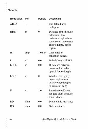
Elements
AREA - - The default areamultiplier
HDIF m 0 Distance of the heavilydiffused or lowresistance region fromsource or drain contactedge to lightly dopedregion
IS amp 1.0e-14 Gate junctionsaturation current
L m 0.0 Default length of FET
LDEL m 0.0 Difference betweendrawn and actual oroptical device length
LDIF m 0 Width of the lightlydoped region fromheavily doped regionto transistor edge
N - 1.0 Emission coefficientfor gate-drain and gate-source diodes
RD ohm 0.0 Drain ohmic resistance
RG ohm 0.0 Gate resistance
Name (Alias) Unit Default Description
8-4 Star-Hspice Quick Reference Guide
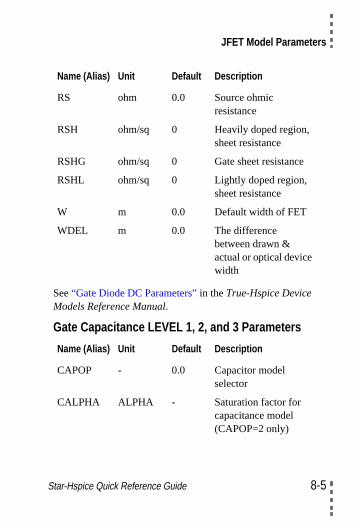
JFET Model Parameters
See“Gate Diode DC Parameters” in theTrue-Hspice DeviceModels Reference Manual.
Gate Capacitance LEVEL 1, 2, and 3 Parameters
RS ohm 0.0 Source ohmicresistance
RSH ohm/sq 0 Heavily doped region,sheet resistance
RSHG ohm/sq 0 Gate sheet resistance
RSHL ohm/sq 0 Lightly doped region,sheet resistance
W m 0.0 Default width of FET
WDEL m 0.0 The differencebetween drawn &actual or optical devicewidth
Name (Alias) Unit Default Description
CAPOP - 0.0 Capacitor modelselector
CALPHA ALPHA - Saturation factor forcapacitance model(CAPOP=2 only)
Name (Alias) Unit Default Description
Star-Hspice Quick Reference Guide 8-5
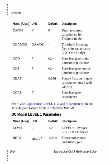
Elements
See“Gate Capacitance LEVEL 1, 2, and 3 Parameters”in theTrue-Hspice Device Models Reference Manual.
DC Model LEVEL 1 Parameters
CAPDS F 0 Drain to sourcecapacitance forTriQuint model
CGAMDS GAMDS - Threshold loweringfactor for capacitance(CAPOP=2 only)
CGD F 0.0 Zero-bias gate-drainjunction capacitance
CGS F 0.0 Zero-bias gate-sourcejunction capacitance
CRAT 0.666 Source fraction of gatecapacitance (used withGCAP)
GCAP F - Zero-bias gatecapacitance
Name (Alias) Unit Default Description
LEVEL - 1.0 LEVEL=1 invokesSPICE JFET model.
BETA amp/V2 1.0e-4 Transconductanceparameter, gain.
Name (Alias) Unit Default Description
8-6 Star-Hspice Quick Reference Guide
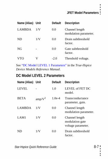
JFET Model Parameters
See“DC Model LEVEL 1 Parameters” in theTrue-HspiceDevice Models Reference Manual.
DC Model LEVEL 2 Parameters
LAMBDA 1/V 0.0 Channel lengthmodulation parameter.
ND 1/V 0.0 Drain subthresholdfactor.
NG - 0.0 Gate subthresholdfactor.
VTO V -2.0 Threshold voltage.
Name (Alias) Unit Default Description
LEVEL - 1.0 LEVEL of FET DCmodel.
BETA amp/V2 1.0e-4 Transconductanceparameter, gain.
LAMBDA 1/V 0.0 Channel lengthmodulation parameter.
LAM1 1/V 0.0 Channel lengthmodulation gatevoltage parameter.
ND 1/V 0.0 Drain subthresholdfactor.
Name (Alias) Unit Default Description
Star-Hspice Quick Reference Guide 8-7
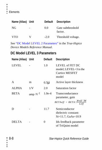
Elements
See“DC Model LEVEL 2 Parameters” in theTrue-HspiceDevice Models Reference Manual.
DC Model LEVEL 3 Parameters
NG - 0.0 Gate subthresholdfactor.
VTO V -2.0 Threshold voltage.
Name (Alias) Unit Default Description
LEVEL - 1.0 LEVEL of FET DCmodel; LEVEL=3 is theCurtice MESFETmodel
A m 0.5µ Active layer thickness
ALPHA 1/V 2.0 Saturation factor
BETA amp /V 2 1.0e-4 Transconductanceparameter, gain
D - 11.7 Semiconductordielectric constant:Si=11.7, GaAs=10.9
DELTA - 0 Ids feedback parameterof TriQuint model
Name (Alias) Unit Default Description
BETAeff BETAWeff M⋅
Leff-----------------------⋅=
8-8 Star-Hspice Quick Reference Guide
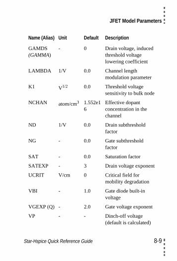
JFET Model Parameters
GAMDS(GAMMA)
- 0 Drain voltage, inducedthreshold voltagelowering coefficient
LAMBDA 1/V 0.0 Channel lengthmodulation parameter
K1 V1/2 0.0 Threshold voltagesensitivity to bulk node
NCHAN atom/cm3 1.552e16
Effective dopantconcentration in thechannel
ND 1/V 0.0 Drain subthresholdfactor
NG - 0.0 Gate subthresholdfactor
SAT - 0.0 Saturation factor
SATEXP - 3 Drain voltage exponent
UCRIT V/cm 0 Critical field formobility degradation
VBI - 1.0 Gate diode built-involtage
VGEXP (Q) - 2.0 Gate voltage exponent
VP - - Dinch-off voltage(default is calculated)
Name (Alias) Unit Default Description
Star-Hspice Quick Reference Guide 8-9
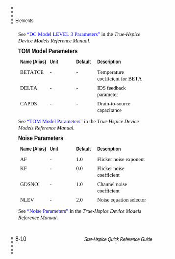
Elements
See“DC Model LEVEL 3 Parameters” in theTrue-HspiceDevice Models Reference Manual.
TOM Model Parameters
See“TOM Model Parameters” in theTrue-Hspice DeviceModels Reference Manual.
Noise Parameters
See“Noise Parameters” in theTrue-Hspice Device ModelsReference Manual.
Name (Alias) Unit Default Description
BETATCE - - Temperaturecoefficient for BETA
DELTA - - IDS feedbackparameter
CAPDS - - Drain-to-sourcecapacitance
Name (Alias) Unit Default Description
AF - 1.0 Flicker noise exponent
KF - 0.0 Flicker noisecoefficient
GDSNOI - 1.0 Channel noisecoefficient
NLEV - 2.0 Noise equation selector
8-10 Star-Hspice Quick Reference Guide
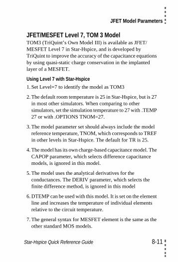
JFET Model Parameters
s
7
P
elF
he
nt
he
JFET/MESFET Level 7, TOM 3 ModelTOM3 (TriQuint’s Own Model III) is available as JFET/MESFET Level 7 in Star-Hspice, and is developed byTriQuint to improve the accuracy of the capacitance equationby using quasi-static charge conservation in the implantedlayer of a MESFET.
Using Level 7 with Star-Hspice
1. Set Level=7 to identify the model as TOM3
2. The default room temperature is 25 in Star-Hspice, but is 2in most other simulators. When comparing to othersimulators, set the simulation temperature to 27 with .TEM27 or with .OPTIONS TNOM=27.
3. The model parameter set should always include the modreference temperature, TNOM, which corresponds to TREin other levels in Star-Hspice. The default for TR is 25.
4. The model has its own charge-based capacitance model. TCAPOP parameter, which selects difference capacitancemodels, is ignored in this model.
5. The model uses the analytical derivatives for theconductances. The DERIV parameter, which selects thefinite difference method, is ignored in this model
6. DTEMP can be used with this model. It is set on the elemeline and increases the temperature of individual elementsrelative to the circuit temperature.
7. The general syntax for MESFET element is the same as tother standard MOS models.
Star-Hspice Quick Reference Guide 8-11
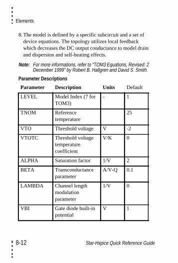
Elements
in
8. The model is defined by a specific subcircuit and a set ofdevice equations. The topology utilizes local feedbackwhich decreases the DC output conductance to model draand dispersion and self-heating effects.
Note: For more informations, refer to “TOM3 Equations, Revised: 2December 1999” by Robert B. Hallgren and David S. Smith.
Parameter Descriptions
Parameter Description Units Default
LEVEL Model Index (7 forTOM3)
- 1
TNOM Referencetemperature
25
VTO Threshold voltage V -2
VTOTC Threshold voltagetemperaturecoefficient
V/K 0
ALPHA Saturation factor 1/V 2
BETA Transconductanceparameter
A/V-Q 0.1
LAMBDA Channel lengthmodulationparameter
1/V 0
VBI Gate diode built-inpotential
V 1
8-12 Star-Hspice Quick Reference Guide
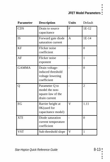
JFET Model Parameters
CDS Drain to sourcecapacitance
F 1E-12
IS Forward gate diodesaturation current
A 1E-14
KF Flicker noisecoefficient
- 0
AF Flicker noiseexponent
- 1
GAMMA Drain voltage-induced thresholdvoltage loweringcoefficient
- 0
Q Parameter Q tomodel the non-square-law of thedrain current
- 2
EG Barrier height at0K(used forcapacitance model)
V 1.11
XTI Diode saturationcurrent temperaturecoefficient
- 0
VST Sub-threshold slope V 1
Parameter Description Units Default
Star-Hspice Quick Reference Guide 8-13
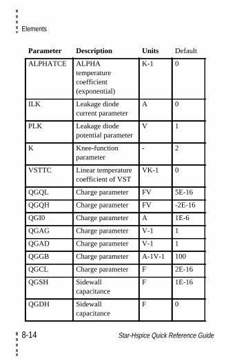
Elements
ALPHATCE ALPHAtemperaturecoefficient(exponential)
K-1 0
ILK Leakage diodecurrent parameter
A 0
PLK Leakage diodepotential parameter
V 1
K Knee-functionparameter
- 2
VSTTC Linear temperaturecoefficient of VST
VK-1 0
QGQL Charge parameter FV 5E-16
QGQH Charge parameter FV -2E-16
QGI0 Charge parameter A 1E-6
QGAG Charge parameter V-1 1
QGAD Charge parameter V-1 1
QGGB Charge parameter A-1V-1 100
QGCL Charge parameter F 2E-16
QGSH Sidewallcapacitance
F 1E-16
QGDH Sidewallcapacitance
F 0
Parameter Description Units Default
8-14 Star-Hspice Quick Reference Guide
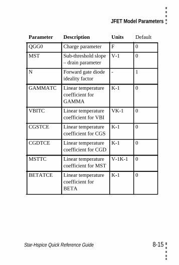
JFET Model Parameters
QGG0 Charge parameter F 0
MST Sub-threshold slope– drain parameter
V-1 0
N Forward gate diodeideality factor
- 1
GAMMATC Linear temperaturecoefficient forGAMMA
K-1 0
VBITC Linear temperaturecoefficient for VBI
VK-1 0
CGSTCE Linear temperaturecoefficient for CGS
K-1 0
CGDTCE Linear temperaturecoefficient for CGD
K-1 0
MSTTC Linear temperaturecoefficient for MST
V-1K-1 0
BETATCE Linear temperaturecoefficient forBETA
K-1 0
Parameter Description Units Default
Star-Hspice Quick Reference Guide 8-15
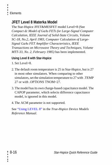
Elements
r
e
7
P
he
JFET Level 8 Materka ModelThe Star-Hspice JFET&MESFET model Level=8 (SeeCompact dc Model of GaAs FETs for Large-Signal ComputeCalculation, IEEE Journal of Solid-State Circuits, VolumeSC-18, No.2, April 1983, Computer Calculation of Large-Signal GaAs FET Amplifier Characteristics, IEEETransactions on Microwave Theory and Techniques, VolumMTT-33, No. 2, February 1985) has been implemented.
Using Level 8 with Star-Hspice
1. Set Level=8.
2. The default room temperature is 25 in Star-Hspice, but is 2in most other simulators. When comparing to othersimulators, set the simulation temperature to 27 with .TEM27 or with .OPTIONS TNOM=27.
3. The model has its own charge-based capacitance model. TCAPOP parameter, which selects difference capacitancemodel, is ignored in this model.
4. The ACM parameter is not supported.
See“Using LEVEL 8” in theTrue-Hspice Device ModelsReference Manual.
8-16 Star-Hspice Quick Reference Guide
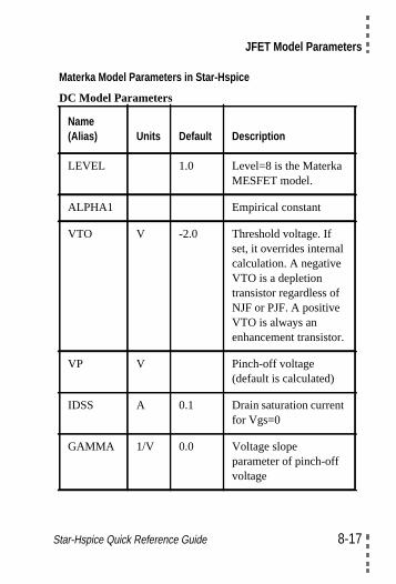
JFET Model Parameters
Materka Model Parameters in Star-Hspice
DC Model Parameters
Name(Alias) Units Default Description
LEVEL 1.0 Level=8 is the MaterkaMESFET model.
ALPHA1 Empirical constant
VTO V -2.0 Threshold voltage. Ifset, it overrides internalcalculation. A negativeVTO is a depletiontransistor regardless ofNJF or PJF. A positiveVTO is always anenhancement transistor.
VP V Pinch-off voltage(default is calculated)
IDSS A 0.1 Drain saturation currentfor Vgs=0
GAMMA 1/V 0.0 Voltage slopeparameter of pinch-offvoltage
Star-Hspice Quick Reference Guide 8-17

Elements
Gate Capacitance Model Parameters
Name (Alias) Units Default Description
CGS F 0.0 Zero-bias gate-source junctioncapacitance
CGD F 0.0 Zero-bias gate-drainjunction capacitance
PB V 0.8 Gate JunctionPotential
N 1.0 Emission coefficientfor gate-drain andgate-source diodes
8-18 Star-Hspice Quick Reference Guide
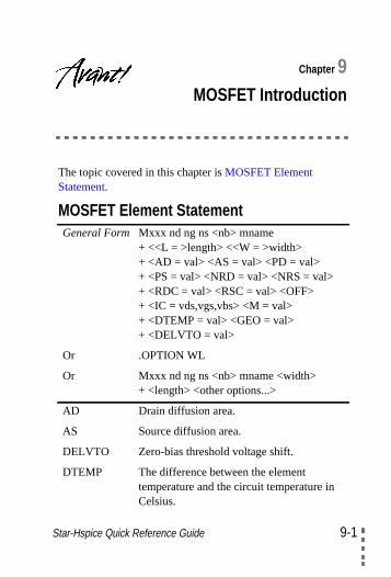
Star-Hspice Quic
9-
Chapter 9MOSFET Introduction
The topic covered in this chapter isMOSFET ElementStatement.
MOSFET Element StatementGeneral Form Mxxx nd ng ns <nb> mname
+ <<L = >length> <<W = >width>+ <AD = val> <AS = val> <PD = val>+ <PS = val> <NRD = val> <NRS = val>+ <RDC = val> <RSC = val> <OFF>+ <IC = vds,vgs,vbs> <M = val>+ <DTEMP = val> <GEO = val>+ <DELVTO = val>
Or
Or
.OPTION WL
Mxxx nd ng ns <nb> mname <width>+ <length> <other options...>
AD Drain diffusion area.
AS Source diffusion area.
DELVTO Zero-bias threshold voltage shift.
DTEMP The difference between the elementtemperature and the circuit temperature inCelsius.
k Reference Guide 9-1
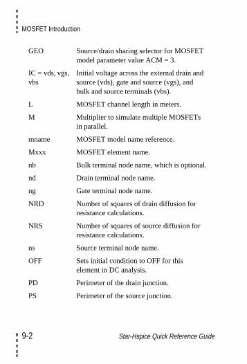
MOSFET Introduction
GEO Source/drain sharing selector for MOSFETmodel parameter value ACM = 3.
IC = vds, vgs,vbs
Initial voltage across the external drain andsource (vds), gate and source (vgs), andbulk and source terminals (vbs).
L MOSFET channel length in meters.
M Multiplier to simulate multiple MOSFETsin parallel.
mname MOSFET model name reference.
Mxxx MOSFET element name.
nb Bulk terminal node name, which is optional.
nd Drain terminal node name.
ng Gate terminal node name.
NRD Number of squares of drain diffusion forresistance calculations.
NRS Number of squares of source diffusion forresistance calculations.
ns Source terminal node name.
OFF Sets initial condition to OFF for thiselement in DC analysis.
PD Perimeter of the drain junction.
PS Perimeter of the source junction.
9-2 Star-Hspice Quick Reference Guide
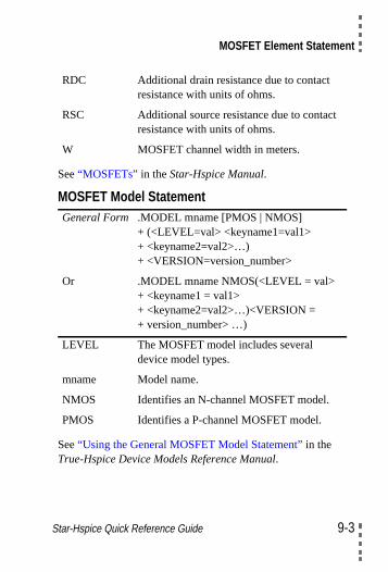
MOSFET Element Statement
t
See“MOSFETs” in theStar-Hspice Manual.
MOSFET Model Statement
See“Using the General MOSFET Model Statement” in theTrue-Hspice Device Models Reference Manual.
RDC Additional drain resistance due to contactresistance with units of ohms.
RSC Additional source resistance due to contacresistance with units of ohms.
W MOSFET channel width in meters.
General Form .MODEL mname [PMOS | NMOS]+ (<LEVEL=val> <keyname1=val1>+ <keyname2=val2>…)+ <VERSION=version_number>
Or .MODEL mname NMOS(<LEVEL = val>+ <keyname1 = val1>+ <keyname2=val2>…)<VERSION =+ version_number> …)
LEVEL The MOSFET model includes severaldevice model types.
mname Model name.
NMOS Identifies an N-channel MOSFET model.
PMOS Identifies a P-channel MOSFET model.
Star-Hspice Quick Reference Guide 9-3
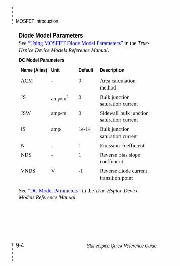
MOSFET Introduction
Diode Model ParametersSee“Using MOSFET Diode Model Parameters” in theTrue-Hspice Device Models Reference Manual.
DC Model Parameters
See“DC Model Parameters” in theTrue-Hspice DeviceModels Reference Manual.
Name (Alias) Unit Default Description
ACM - 0 Area calculationmethod
JS amp/m2 0 Bulk junctionsaturation current
JSW amp/m 0 Sidewall bulk junctionsaturation current
IS amp 1e-14 Bulk junctionsaturation current
N - 1 Emission coefficient
NDS - 1 Reverse bias slopecoefficient
VNDS V -1 Reverse diode currenttransition point
9-4 Star-Hspice Quick Reference Guide
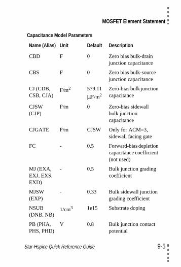
MOSFET Element Statement
Capacitance Model Parameters
Name (Alias) Unit Default Description
CBD F 0 Zero bias bulk-drainjunction capacitance
CBS F 0 Zero bias bulk-sourcejunction capacitance
CJ (CDB,CSB, CJA)
F/m2 579.11
µF/m2
Zero-bias bulk junctioncapacitance
CJSW(CJP)
F/m 0 Zero-bias sidewallbulk junctioncapacitance
CJGATE F/m CJSW Only for ACM=3,sidewall facing gate
FC - 0.5 Forward-bias depletioncapacitance coefficient(not used)
MJ (EXA,EXJ, EXS,EXD)
- 0.5 Bulk junction gradingcoefficient
MJSW(EXP)
- 0.33 Bulk sidewall junctiongrading coefficient
NSUB(DNB, NB)
1/cm3 1e15 Substrate doping
PB (PHA,PHS, PHD)
V 0.8 Bulk junction contactpotential
Star-Hspice Quick Reference Guide 9-5
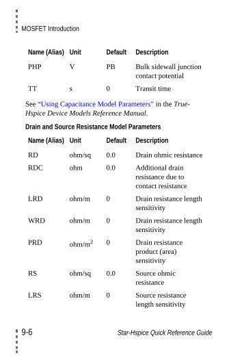
MOSFET Introduction
See“Using Capacitance Model Parameters” in theTrue-Hspice Device Models Reference Manual.
Drain and Source Resistance Model Parameters
PHP V PB Bulk sidewall junctioncontact potential
TT s 0 Transit time
Name (Alias) Unit Default Description
RD ohm/sq 0.0 Drain ohmic resistance
RDC ohm 0.0 Additional drainresistance due tocontact resistance
LRD ohm/m 0 Drain resistance lengthsensitivity
WRD ohm/m 0 Drain resistance lengthsensitivity
PRD ohm/m2 0 Drain resistanceproduct (area)sensitivity
RS ohm/sq 0.0 Source ohmicresistance
LRS ohm/m 0 Source resistancelength sensitivity
Name (Alias) Unit Default Description
9-6 Star-Hspice Quick Reference Guide
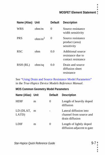
MOSFET Element Statement
”
See“Using Drain and Source Resistance Model Parametersin theTrue-Hspice Device Models Reference Manual.MOS Common Geometry Model Parameters
WRS ohm/m 0 Source resistancewidth sensitivity
PRS ohm/m2 0 Source resistanceproduct (area)sensitivity
RSC ohm 0.0 Additional sourceresistance due tocontact resistance
RSH (RL) ohm/sq 0.0 Drain and sourcediffusion sheetresistance
Name (Alias) Unit Default Description
HDIF m 0 Length of heavily dopeddiffusion
LD (DLAT,LATD)
m - Lateral diffusion intochannel from source anddrain diffusion
LDIF m 0 Length of lightly dopeddiffusion adjacent to gate
Name (Alias) Unit Default Description
Star-Hspice Quick Reference Guide 9-7
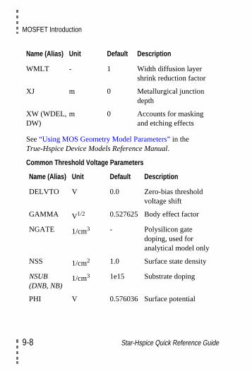
MOSFET Introduction
See“Using MOS Geometry Model Parameters” in theTrue-Hspice Device Models Reference Manual.
Common Threshold Voltage Parameters
WMLT - 1 Width diffusion layershrink reduction factor
XJ m 0 Metallurgical junctiondepth
XW (WDEL,DW)
m 0 Accounts for maskingand etching effects
Name (Alias) Unit Default Description
DELVTO V 0.0 Zero-bias thresholdvoltage shift
GAMMA V1/2 0.527625 Body effect factor
NGATE 1/cm3 - Polysilicon gatedoping, used foranalytical model only
NSS 1/cm2 1.0 Surface state density
NSUB(DNB, NB)
1/cm3 1e15 Substrate doping
PHI V 0.576036 Surface potential
Name (Alias) Unit Default Description
9-8 Star-Hspice Quick Reference Guide
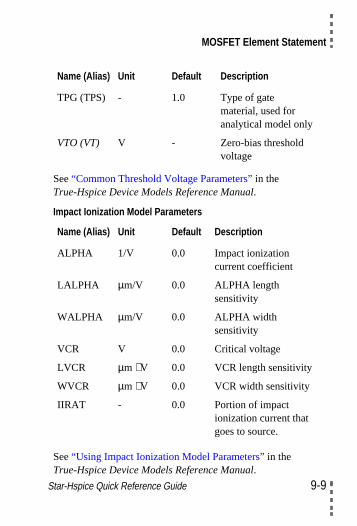
MOSFET Element Statement
Star-Hspice Quick Reference Guide 9-9
See“Common Threshold Voltage Parameters” in theTrue-Hspice Device Models Reference Manual.
Impact Ionization Model Parameters
See“Using Impact Ionization Model Parameters” in theTrue-Hspice Device Models Reference Manual.
TPG (TPS) - 1.0 Type of gatematerial, used foranalytical model only
VTO (VT) V - Zero-bias thresholdvoltage
Name (Alias) Unit Default Description
ALPHA 1/V 0.0 Impact ionizationcurrent coefficient
LALPHA µm/V 0.0 ALPHA lengthsensitivity
WALPHA µm/V 0.0 ALPHA widthsensitivity
VCR V 0.0 Critical voltage
LVCR µm ⋅ V 0.0 VCR length sensitivity
WVCR µm ⋅ V 0.0 VCR width sensitivity
IIRAT - 0.0 Portion of impactionization current thatgoes to source.
Name (Alias) Unit Default Description
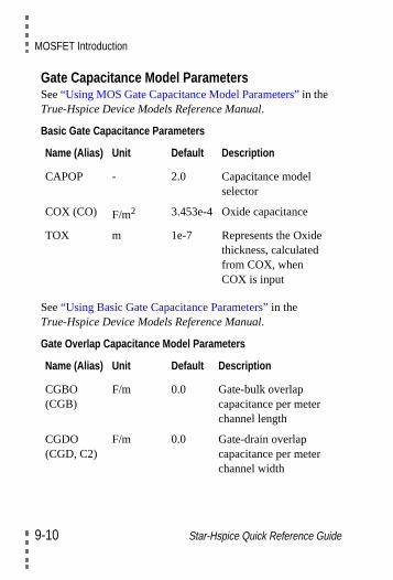
MOSFET Introduction
Gate Capacitance Model ParametersSee“Using MOS Gate Capacitance Model Parameters”in theTrue-Hspice Device Models Reference Manual.
Basic Gate Capacitance Parameters
See“Using Basic Gate Capacitance Parameters” in theTrue-Hspice Device Models Reference Manual.
Gate Overlap Capacitance Model Parameters
Name (Alias) Unit Default Description
CAPOP - 2.0 Capacitance modelselector
COX (CO) F/m2 3.453e-4 Oxide capacitance
TOX m 1e-7 Represents the Oxidethickness, calculatedfrom COX, whenCOX is input
Name (Alias) Unit Default Description
CGBO(CGB)
F/m 0.0 Gate-bulk overlapcapacitance per meterchannel length
CGDO(CGD, C2)
F/m 0.0 Gate-drain overlapcapacitance per meterchannel width
9-10 Star-Hspice Quick Reference Guide
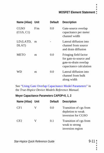
MOSFET Element Statement
See“Using Gate Overlap Capacitance Model Parameters” intheTrue-Hspice Device Models Reference Manual.
Meyer Capacitance Parameters CAPOP=0, 1, 2
CGSO(CGS, C1)
F/m 0.0 Gate-source overlapcapacitance per meterchannel width
LD (LATD,DLAT)
m - Lateral diffusion intochannel from sourceand drain diffusion
METO m 0.0 Fringing field factorfor gate-to-source andgate-to-drain overlapcapacitance calculation
WD m 0.0 Lateral diffusion intochannel from bulkalong width
Name (Alias) Unit Default Description
CF1 V 0.0 Transition of cgs fromdepletion to weakinversion for CGSO
CF2 V 0.1 Transition of cgs fromweak to stronginversion region
Name (Alias) Unit Default Description
Star-Hspice Quick Reference Guide 9-11
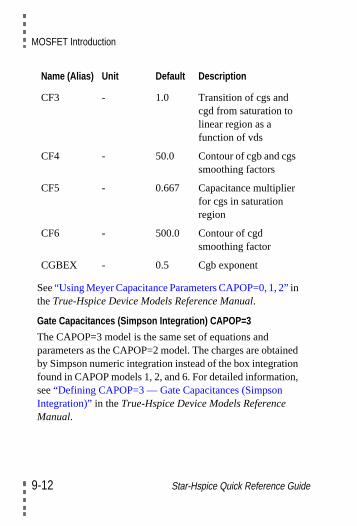
MOSFET Introduction
edn,
See“Using Meyer Capacitance Parameters CAPOP=0, 1, 2”intheTrue-Hspice Device Models Reference Manual.
Gate Capacitances (Simpson Integration) CAPOP=3
The CAPOP=3 model is the same set of equations andparameters as the CAPOP=2 model. The charges are obtainby Simpson numeric integration instead of the box integratiofound in CAPOP models 1, 2, and 6. For detailed informationsee“Defining CAPOP=3 — Gate Capacitances (SimpsonIntegration)” in theTrue-Hspice Device Models ReferenceManual.
CF3 - 1.0 Transition of cgs andcgd from saturation tolinear region as afunction of vds
CF4 - 50.0 Contour of cgb and cgssmoothing factors
CF5 - 0.667 Capacitance multiplierfor cgs in saturationregion
CF6 - 500.0 Contour of cgdsmoothing factor
CGBEX - 0.5 Cgb exponent
Name (Alias) Unit Default Description
9-12 Star-Hspice Quick Reference Guide
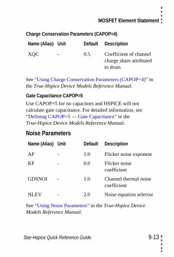
MOSFET Element Statement
Charge Conservation Parameters (CAPOP=4)
See“Using Charge Conservation Parameters (CAPOP=4)”intheTrue-Hspice Device Models Reference Manual.
Gate Capacitance CAPOP=5
Use CAPOP=5 for no capacitors and HSPICE will notcalculate gate capacitance. For detailed information, see“Defining CAPOP=5 — Gate Capacitance” in theTrue-Hspice Device Models Reference Manual.
Noise Parameters
See“Using Noise Parameters” in theTrue-Hspice DeviceModels Reference Manual.
Name (Alias) Unit Default Description
XQC - 0.5 Coefficient of channelcharge share attributedto drain
Name (Alias) Unit Default Description
AF - 1.0 Flicker noise exponent
KF - 0.0 Flicker noisecoefficient
GDSNOI - 1.0 Channel thermal noisecoefficient
NLEV - 2.0 Noise equation selector
Star-Hspice Quick Reference Guide 9-13
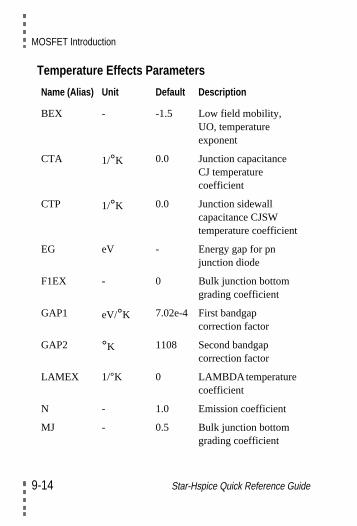
MOSFET Introduction
Temperature Effects Parameters
Name (Alias) Unit Default Description
BEX - -1.5 Low field mobility,UO, temperatureexponent
CTA 1/°K 0.0 Junction capacitanceCJ temperaturecoefficient
CTP 1/°K 0.0 Junction sidewallcapacitance CJSWtemperature coefficient
EG eV - Energy gap for pnjunction diode
F1EX - 0 Bulk junction bottomgrading coefficient
GAP1 eV/°K 7.02e-4 First bandgapcorrection factor
GAP2 °K 1108 Second bandgapcorrection factor
LAMEX 1/°K 0 LAMBDAtemperaturecoefficient
N - 1.0 Emission coefficient
MJ - 0.5 Bulk junction bottomgrading coefficient
9-14 Star-Hspice Quick Reference Guide
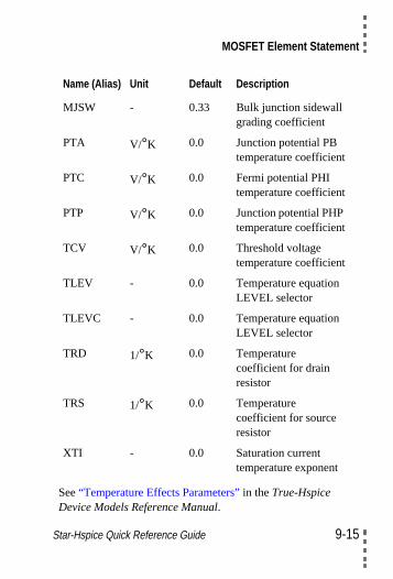
MOSFET Element Statement
See“Temperature Effects Parameters” in theTrue-HspiceDevice Models Reference Manual.
MJSW - 0.33 Bulk junction sidewallgrading coefficient
PTA V/°K 0.0 Junction potential PBtemperature coefficient
PTC V/°K 0.0 Fermi potential PHItemperature coefficient
PTP V/°K 0.0 Junction potential PHPtemperature coefficient
TCV V/°K 0.0 Threshold voltagetemperature coefficient
TLEV - 0.0 Temperature equationLEVEL selector
TLEVC - 0.0 Temperature equationLEVEL selector
TRD 1/°K 0.0 Temperaturecoefficient for drainresistor
TRS 1/°K 0.0 Temperaturecoefficient for sourceresistor
XTI - 0.0 Saturation currenttemperature exponent
Name (Alias) Unit Default Description
Star-Hspice Quick Reference Guide 9-15

MOSFET Introduction
9-16 Star-Hspice Quick Reference Guide
Star-Hspice Quic
10-
Chapter 10MOSFET Models
lyin
This chapter briefly introduces MOSFET usage and concisedescribes the commonly used models. The topics covered this chapter are:
• Model Table
• LEVEL 47 BSIM3 Version 2 MOS Model
• LEVELs 49 and 53 BSIM3v3 MOS Models
• LEVEL 50 Philips MOS9 Model
• LEVEL 54 BSIM 4.0 Model
• LEVEL 55 EPFL-EKV MOSFET Model
• LEVEL 57 UC Berkeley BSIM3-SOI Model
• LEVEL 58 University of Florida SOI Model
• LEVEL 59 UC Berkeley BSIM3-SOI FD Model
• LEVEL 60 UC Berkeley BSIM3-SOI DD Model
• LEVEL 61 RPI a-Si TFT Model
• LEVEL 62 RPI Poli-Si TFT Model
• MOS Level 63, Philips MOS11 Model
For more information about these and other models, seeChapters 21 and 22 in theStar-Hspice Manual.
k Reference Guide 10-1
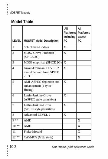
MOSFET Models
Model Table
LEVEL MOSFET Model Description
AllPlatformsincludingPC
AllPlatformsexceptPC
1 Schichman-Hodges X
2 MOS2 Grove-Frohman(SPICE 2G)
X
3 MOS3 empirical (SPICE 2G) X
4 Grove-Frohman: LEVEL 2model derived from SPICE2E.3
X
5 AMI-ASPEC depletion andenhancement (Taylor-Huang)
X
6 Lattin-Jenkins-Grove(ASPEC style parasitics)
X
7 Lattin-Jenkins-Grove(SPICE style parasitics)
X
8 Advanced LEVEL 2 X
9 ** AMD X
10 ** AMD X
11 Fluke-Mosaid X
12 ** CASMOS (GTE style) X
10-2 Star-Hspice Quick Reference Guide
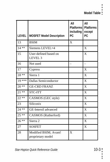
Model Table
13 BSIM X
14 ** Siemens LEVEL=4 X
15 User-defined based onLEVEL 3
X
16 Not used – –
17 Cypress X
18 ** Sierra 1 X
19 *** Dallas Semiconductor X
20 ** GE-CRD FRANZ X
21 ** STC-ITT X
22 ** CASMOS (GEC style) X
23 Siliconix X
24 ** GE-Intersil advanced X
25 ** CASMOS (Rutherford) X
26 ** Sierra 2 X
27 SOSFET X
28 Modified BSIM; Avant!proprietary model
X
LEVEL MOSFET Model Description
AllPlatformsincludingPC
AllPlatformsexceptPC
Star-Hspice Quick Reference Guide 10-3
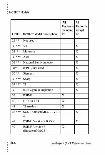
MOSFET Models
29 *** Not used – –
30 *** VTI X
31*** Motorola X
32 *** AMD X
33 *** National Semiconductor X
34* (EPFL) not used X
35 ** Siemens X
36 *** Sharp X
37 *** TI X
38 IDS: Cypress Depletion X
39 BSIM2 X
40 HP a-Si TFT X
41 TI Analog X
46 *** SGS-Thomson MOS LEVEL3
X
47 BSIM3 Version 2.0 MOS X
49 BSIM3 Version 3(Enhanced) MOS
X
LEVEL MOSFET Model Description
AllPlatformsincludingPC
AllPlatformsexceptPC
10-4 Star-Hspice Quick Reference Guide
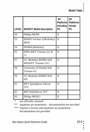
Model Table
d
50 Philips MOS9 X
53 BSIM3 Version 3 (Berkeley)MOS
X
54 BSIM4 (Berkeley) X
55 EPFL-EKV Version 2.6, R11
X
57 UC Berkeley BSIM3-SOIMOSFET Version 2.0.1
X
58 University of Florida SOIVersion 4.5
X
59 UC Berkeley BSIM3-SOI-FD
X
61 RPT Amorphous SiliconTFT
X
62 RPT PolySilicon TFT X
63 Philips MOS11 X
* not officially released** equations are proprietary – documentation not provide*** requires a license and equations are proprietary –
documentation not provided
LEVEL MOSFET Model Description
AllPlatformsincludingPC
AllPlatformsexceptPC
Star-Hspice Quick Reference Guide 10-5
MOSFET Models
orls
ly
For detailed information, see“Selecting MOSFET ModelLEVELs” in theTrue-Hspice Device Models ReferenceManual.
The remainder of this section provides the general syntax fand basic description of the commonly used MOSFET mode(LEVEL 47 and higher).
LEVEL 47 BSIM3 Version 2 MOS ModelThe Star-Hspice LEVEL 47 model uses the general modelstatement described in“MOSFET Model Statement” on page9-3. It also uses the same:
• Model parameters for source/drain diode current,capacitance, and resistance (ACM controls the choice ofsource/drain equations)
• Noise equations as the other LEVELs (NLEV controls thechoice of noise equations)
as do the other Star-Hspice MOS LEVELs. Like all models inStar-Hspice, LEVEL 47 can be parameterized. This is usefufor modeling process skew, either by worst-case corners or bMonte Carlo. For detailed information, see“LEVEL 47BSIM3 Version 2 MOS Model” in theTrue-Hspice DeviceModels Reference Manual.
Using BSIM3 Version 2 with Star-Hspice• Set LEVEL=47 to identify the model as a BSIM3 model.
• The default setting is CAPOP=13 (BSIM1 charge-conserving capacitance model).
10-6 Star-Hspice Quick Reference Guide
LEVEL 47 BSIM3 Version 2 MOS Model
s
t
.
s
• TheTNOM model parameter is an alias forTREF (forcompatibility with SPICE3).
• The default room temperature is 25°C in Star-Hspice, but27°C in SPICE3; if BSIM3 model parameters are specifiedat 27°C, use TREF=27.
• The default ofDERIVis zero (analytical method); if set to 1(finite difference method), it gives more accurate derivativebut consumes more CPU time.
• Three ways for the BSIM3 model to calculateVth:
- User-specifiedK1 andK2 values.
- GAMMA1, GAMMA2, VBM, andVBX values entered inthe .MODEL statement.
- User-specifiedNPEAK, NSUB, XT, andVBM values.
• NPEAK andU0 can be in meters or centimeters. You mus
enter the parameterNSUB in cm-3 units.
• VTH0 for P-channel in the .MODEL statement is negative
• The default value ofKT1 is -0.11.
• LITL may not go below a minimum value of 1.0e-9 m.
• VSAT, after temperature adjustment, is not allowed to gobelow a minimum value of 1.0e4 m/sec, to assure that it ipositive after temperature compensation.
• The model parameters that accommodate temperaturedependencies areKT1andKT2for VTH, UTEfor U0, ATforVSAT, UA1 for UA, UB1 for UB, andUC1 for UC.
Star-Hspice Quick Reference Guide 10-7
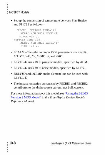
MOSFET Models
e
.
2
• Set up the conversion of temperature between Star-Hspicand SPICE3 as follows:
SPICE3:.OPTIONS TEMP=125.MODEL NCH NMOS LEVEL=8+TNOM =27 ...
HSPICE:.TEMP 125.MODEL NCH NMOS LEVEL=47+TREF =27 ...
• SCALM affects the common MOS parameters, such asXL,LD, XW, WD, CJ, CJSW, JS, andJSW.
• LEVEL 47 uses MOS parasitic models, specified by ACM
• LEVEL 47 uses MOS noise models, specified by NLEV.
• DELVTOandDTEMPon the element line can be used withLEVEL 47.
• The impact ionization current set by PSCBE1 and PSCBEcontributes to the drain-source current; not bulk current.
For more information about this model, see“Using the BSIM3Version 2 MOS Model” in theTrue-Hspice Device ModelsReference Manual.
10-8 Star-Hspice Quick Reference Guide
LEVELs 49 and 53 BSIM3v3 MOS Models
ed
,
t
LEVELs 49 and 53 BSIM3v3 MOS ModelsLEVELs 49 and 53 use the general model statement describin “MOSFET Model Statement” on page 9-3. They alsomaintain compliance with the UC Berkeley release ofBSIM3v3. The basic differences between LEVEL 49 and 53are:
• LEVEL 49 was designed to be compliant with BerkeleyBSIM3v3, but enhanced for higher speed. To achieve thisACM defaults to 0 in LEVEL 49; compliance with BerkeleyBSIM3v3 requires ACM=10.
• LEVEL 53, on the other hand, is completely compliant withBerkeley BSIM3v3; all Hspice-specific parameters defaulto OFF.
For more information about this model, see“LEVELs 49 and53 BSIM3v3 MOS Models” in theTrue-Hspice DeviceModels Reference Manual.
Selecting Model VersionsThe recommended BSIM3v3 model specification isLEVEL=49, VERSION=3.22. See“Selecting ModelVersions” in theTrue-Hspice Device Models ReferenceManual.
Star-Hspice Quick Reference Guide 10-9
MOSFET Models
,
LEVEL 50 Philips MOS9 ModelThe Philips MOS9 model, available in Star-Hspice asLEVEL 50, uses the general model statement described in“MOSFET Model Statement” on page 9-3. Specific changesinclude:
• The ACM Parasitic Diode Model, using parameters JS,JSW, N, CJ, CJSW, CJGATE, MJ, MJSW, PB, PHP, ACMand HDIF was added.
• The Philips JUNCAP Parasitic Diode Model were added.
• The model parameter JUNCAP=1 selects the JUNCAPModel, JUNCAP=0 (default) selects the Hspice ACMModel.
• Gate noise current is not available.
For more information, see
http://www.us.semiconductors.com/Philips_Models.
Also, see“LEVEL 50 Philips MOS9 Model” in theTrue-Hspice Device Models Reference Manual.
Using the Philips MOS9 Model in Star-Hspice• Set LEVEL=50 to identify the model as Philips MOS
Model 9.
• The default room temperature is 25°C in Star-Hspice, but27°C in SPICE3.
10-10 Star-Hspice Quick Reference Guide
LEVEL 54 BSIM 4.0 Model
;
s;
in
,
t
• Always include TR, which corresponds to TREF in otherLEVELs in Star-Hspice. The default for TR is 21.0°C, tomatch the Philips simulator.
• The model has its own charge-based capacitance modelCAPOP is ignored for this model.
• The model uses analytical derivatives for the conductanceDERIV is ignored for this model.
• DTEMP can be used with this model.
• Since defaults are non-zero, every model parameter listedLEVEL 50 Model Parameters table should be set inthe .MODEL statement.
• Select one of two available parasitic junction diode modelsACM and JUNCAP. JUNCAP=1 selects the PhilipsJUNCAP model, JUNCAP=0 (default) selects theStar-Hspice ACM model.
See“Using the Philips MOS9 Model in Star-Hspice” in theTrue-Hspice Device Models Reference Manual.
LEVEL 54 BSIM 4.0 ModelThe UC Berkeley BSIM 4.0.0 MOS model is the LEVEL 54Star-Hspice model; it is designed for modeling sub-0.13micron CMOS technology and RF high-speed CMOS circuisimulation. LEVEL 54 uses the general model statementdescribed in“MOSFET Model Statement” on page 9-3.
BSIM4.0.0 has major improvements and additions overBSIM3v3, including:
Star-Hspice Quick Reference Guide 10-11
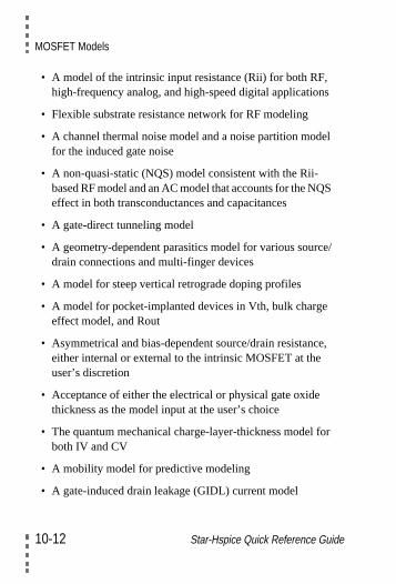
MOSFET Models
s
l
S
e/
e,
or
• A model of the intrinsic input resistance (Rii) for both RF,high-frequency analog, and high-speed digital application
• Flexible substrate resistance network for RF modeling
• A channel thermal noise model and a noise partition modefor the induced gate noise
• A non-quasi-static (NQS) model consistent with the Rii-based RF model and an AC model that accounts for the NQeffect in both transconductances and capacitances
• A gate-direct tunneling model
• A geometry-dependent parasitics model for various sourcdrain connections and multi-finger devices
• A model for steep vertical retrograde doping profiles
• A model for pocket-implanted devices in Vth, bulk chargeeffect model, and Rout
• Asymmetrical and bias-dependent source/drain resistanceither internal or external to the intrinsic MOSFET at theuser’s discretion
• Acceptance of either the electrical or physical gate oxidethickness as the model input at the user’s choice
• The quantum mechanical charge-layer-thickness model fboth IV and CV
• A mobility model for predictive modeling
• A gate-induced drain leakage (GIDL) current model
10-12 Star-Hspice Quick Reference Guide
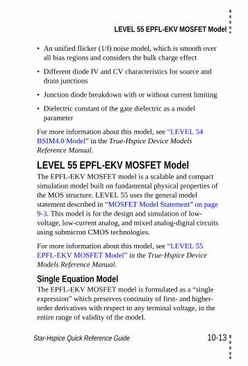
LEVEL 55 EPFL-EKV MOSFET Model
f
s
• An unified flicker (1/f) noise model, which is smooth overall bias regions and considers the bulk charge effect
• Different diode IV and CV characteristics for source anddrain junctions
• Junction diode breakdown with or without current limiting
• Dielectric constant of the gate dielectric as a modelparameter
For more information about this model, see“LEVEL 54BSIM4.0 Model” in theTrue-Hspice Device ModelsReference Manual.
LEVEL 55 EPFL-EKV MOSFET ModelThe EPFL-EKV MOSFET model is a scalable and compactsimulation model built on fundamental physical properties othe MOS structure. LEVEL 55 uses the general modelstatement described in“MOSFET Model Statement” on page9-3. This model is for the design and simulation of low-voltage, low-current analog, and mixed analog-digital circuitusing submicron CMOS technologies.
For more information about this model, see“LEVEL 55EPFL-EKV MOSFET Model”in theTrue-Hspice DeviceModels Reference Manual.
Single Equation ModelThe EPFL-EKV MOSFET model is formulated as a “singleexpression” which preserves continuity of first- and higher-order derivatives with respect to any terminal voltage, in theentire range of validity of the model.
Star-Hspice Quick Reference Guide 10-13
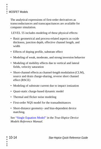
MOSFET Models
or
),
The analytical expressions of first-order derivatives astransconductances and transcapacitances are available forcomputer simulation.
LEVEL 55 includes modeling of these physical effects:
• Basic geometrical and process-related aspects as oxidethickness, junction depth, effective channel length, andwidth
• Effects of doping profile, substrate effect
• Modeling of weak, moderate, and strong inversion behavi
• Modeling of mobility effects due to vertical and lateralfields, velocity saturation
• Short-channel effects as channel-length modulation (CLMsource and drain charge-sharing, reverse short channeleffect (RSCE)
• Modeling of substrate current due to impact ionization
• Quasi-static charge-based dynamic model
• Thermal and flicker noise modeling
• First-order NQS model for the transadmittances
• Short-distance geometry- and bias-dependent devicematching.
See“Single Equation Model” in theTrue-Hspice DeviceModels Reference Manual.
10-14 Star-Hspice Quick Reference Guide

LEVEL 57 UC Berkeley BSIM3-SOI Model
le.S
er.
Coherence of Static and Dynamic ModelsAll aspects regarding the static, the quasi-static and NQSdynamic and noise models are derived from the normalizedtransconductance-to-current ratio. Symmetric normalizedforward and reverse currents are used throughout theseexpressions. For quasi-static dynamic operation, both acharge-based model for the node charges and trans-capacitances, and a simpler capacitances model are availabThe dynamic model, including the time constant for the NQmodel, is described in symmetrical terms of the forward andreverse normalized currents. The charge formulation is furthused to express effective mobility dependence of local field
See“Coherence of Static and Dynamic Models” in theTrue-Hspice Device Models Reference Manual.
LEVEL 57 UC Berkeley BSIM3-SOI ModelGeneral Form Mxxx nd ng ns ne <np> <nb> <nT> mname
+ <L=val> <W=val> <M=val> <AD=val>+ <AS=val> <PD=val> <PS=val>+ <NRD=val> <NRS=val> <NRB=val>+ <RTH0=val> <CTH0=val> <NBC=val>+ <NSEG=val> <PDBCP=val>+ <PSBCP=val> <AGBCP=val>+ <AEBCP=val> <VBSUSR=val>+ <TNODEOUT> <off> <BJToff=val>+ <IC=Vds, Vgs, Vbs, Ves, Vps>
AD Drain diffusion area
Star-Hspice Quick Reference Guide 10-15
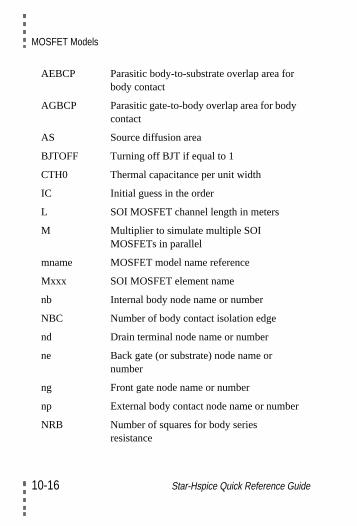
MOSFET Models
r
r
10-16 Star-Hspice Quick Reference Guide
AEBCP Parasitic body-to-substrate overlap area fobody contact
AGBCP Parasitic gate-to-body overlap area for bodycontact
AS Source diffusion area
BJTOFF Turning off BJT if equal to 1
CTH0 Thermal capacitance per unit width
IC Initial guess in the order
L SOI MOSFET channel length in meters
M Multiplier to simulate multiple SOIMOSFETs in parallel
mname MOSFET model name reference
Mxxx SOI MOSFET element name
nb Internal body node name or number
NBC Number of body contact isolation edge
nd Drain terminal node name or number
ne Back gate (or substrate) node name ornumber
ng Front gate node name or number
np External body contact node name or numbe
NRB Number of squares for body seriesresistance
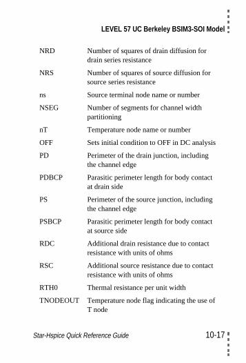
LEVEL 57 UC Berkeley BSIM3-SOI Model
t
NRD Number of squares of drain diffusion fordrain series resistance
NRS Number of squares of source diffusion forsource series resistance
ns Source terminal node name or number
NSEG Number of segments for channel widthpartitioning
nT Temperature node name or number
OFF Sets initial condition to OFF in DC analysis
PD Perimeter of the drain junction, includingthe channel edge
PDBCP Parasitic perimeter length for body contactat drain side
PS Perimeter of the source junction, includingthe channel edge
PSBCP Parasitic perimeter length for body contactat source side
RDC Additional drain resistance due to contactresistance with units of ohms
RSC Additional source resistance due to contacresistance with units of ohms
RTH0 Thermal resistance per unit width
TNODEOUT Temperature node flag indicating the use ofT node
Star-Hspice Quick Reference Guide 10-17
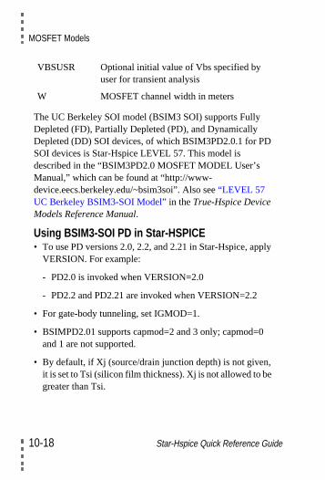
MOSFET Models
ly
The UC Berkeley SOI model (BSIM3 SOI) supports FullyDepleted (FD), Partially Depleted (PD), and DynamicallyDepleted (DD) SOI devices, of which BSIM3PD2.0.1 for PDSOI devices is Star-Hspice LEVEL 57. This model isdescribed in the “BSIM3PD2.0 MOSFET MODEL User’sManual,” which can be found at “http://www-device.eecs.berkeley.edu/~bsim3soi”. Also see“LEVEL 57UC Berkeley BSIM3-SOI Model” in theTrue-Hspice DeviceModels Reference Manual.
Using BSIM3-SOI PD in Star-HSPICE• To use PD versions 2.0, 2.2, and 2.21 in Star-Hspice, app
VERSION. For example:
- PD2.0 is invoked when VERSION=2.0
- PD2.2 and PD2.21 are invoked when VERSION=2.2
• For gate-body tunneling, set IGMOD=1.
• BSIMPD2.01 supports capmod=2 and 3 only; capmod=0and 1 are not supported.
• By default, if Xj (source/drain junction depth) is not given,it is set to Tsi (silicon film thickness). Xj is not allowed to begreater than Tsi.
VBSUSR Optional initial value of Vbs specified byuser for transient analysis
W MOSFET channel width in meters
10-18 Star-Hspice Quick Reference Guide

LEVEL 57 UC Berkeley BSIM3-SOI Model
,e/.y
• BSIMPD refers substrate to the silicon below buried oxidenot the well region in BSIM3. It is used to calculate backgatflatband voltage (Vfbb) and parameters related to sourcedrain diffusion bottom capacitance (Vsdth, Vsdfb, Csdmin)Positive NSUB means the same type of doping as the bodand negative NSUB means opposite type of doping.
For more information about this model, see“Using BSIM3-SOI PD” in theTrue-Hspice Device Models ReferenceManual.
LEVEL 57 Template Output
Name Alias Description
L LV1 Channel length (L)
W LV2 Channel width (W)
AD LV3 Area of the drain diode (AD)
AS LV4 Area of the source diode (AS)
ICVDS LV5 Initial condition for drain-sourcevoltage (VDS)
ICVGS LV6 Initial condition for gate-sourcevoltage (VGS)
ICVES LV7 Initial condition for Substrate-sourcevoltage (VES)
VTH LV9 Threshold voltage (bias dependent)
VDSAT LV10 Saturation voltage (VDSAT)
PD LV11 Drain diode periphery (PD)
Star-Hspice Quick Reference Guide 10-19
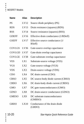
MOSFET Models
PS LV12 Source diode periphery (PS)
RDS LV13 Drain resistance (squares) (RDS)
RSS LV14 Source resistance (squares) (RSS)
GDEFF LV16 Effective drain conductance (1/RDeff)
GSEFF LV17 Effective source conductance (1/RSeff)
COVLGS LV36 Gate-source overlap capacitance
COVLGD LV37 Gate-drain overlap capacitance
COVLGE LV38 Gate-substrate overlap capacitance
VES LX1 Substrate-source voltage (VES)
VGS LX2 Gate-source voltage (VGS)
VDS LX3 Drain-source voltage (VDS)
CDO LX4 DC drain current (CDO)
CBSO LX5 DC source-body diode current (CBSO)
CBDO LX6 DC drain-body diode current (CBDO)
GMO LX7 DC gate transconductance (GMO)
GDSO LX8 DC drain-source conductance (GDSO)
GMESO LX9 DC substrate transconductance(GMBSO)
GBDO LX10 Conductance of the drain diode(GBDO)
Name Alias Description
10-20 Star-Hspice Quick Reference Guide
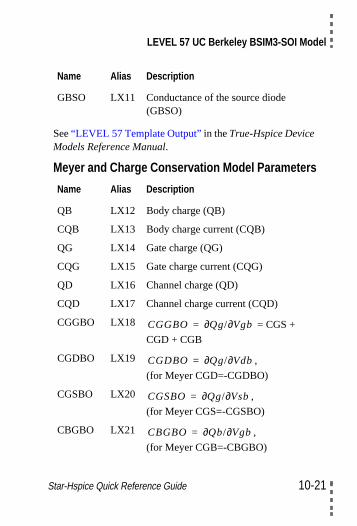
LEVEL 57 UC Berkeley BSIM3-SOI Model
See“LEVEL 57 Template Output”in theTrue-Hspice DeviceModels Reference Manual.
Meyer and Charge Conservation Model Parameters
GBSO LX11 Conductance of the source diode(GBSO)
Name Alias Description
QB LX12 Body charge (QB)
CQB LX13 Body charge current (CQB)
QG LX14 Gate charge (QG)
CQG LX15 Gate charge current (CQG)
QD LX16 Channel charge (QD)
CQD LX17 Channel charge current (CQD)
CGGBO LX18 = CGS +
CGD + CGB
CGDBO LX19 ,
(for Meyer CGD=-CGDBO)
CGSBO LX20 ,
(for Meyer CGS=-CGSBO)
CBGBO LX21 ,
(for Meyer CGB=-CBGBO)
Name Alias Description
CGGBO Qg/ Vgb∂∂=
CGDBO Qg/ Vdb∂∂=
CGSBO Qg/ Vsb∂∂=
CBGBO Qb/ Vgb∂∂=
Star-Hspice Quick Reference Guide 10-21
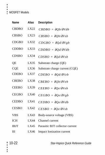
MOSFET Models
CBDBO LX22
CBSBO LX23
CDGBO LX32
CDDBO LX33
CDSBO LX34
QE LX35 Substrate charge (QE)
CQE LX36 Substrate charge current (CQE)
CDEBO LX37
CBEBO LX38
CEEBO LX39
CEGBO LX40
CEDBO LX41
CESBO LX42
VBS LX43 Body-source voltage (VBS)
ICH LX44 Channel current
IBJT LX45 Parasitic BJT collector current
III LX46 Impact Ionization current
Name Alias Description
CBDBO Qb/ Vdb∂∂=
CBSBO Qb/ Vsb∂∂=
CDGBO Qd/ Vgb∂∂=
CDDBO Qd/ Vdb∂∂=
CDSBO Qd/ Vsb∂∂=
CDEBO Qd/ Veb∂∂=
CBEBO Qb/ Veb∂∂=
CEEBO Qe/ Veb∂∂=
CEGBO Qe/ Vgb∂∂=
CEDBO Qe/ Vdb∂∂=
CESBO Qe/ Vsb∂∂=
10-22 Star-Hspice Quick Reference Guide
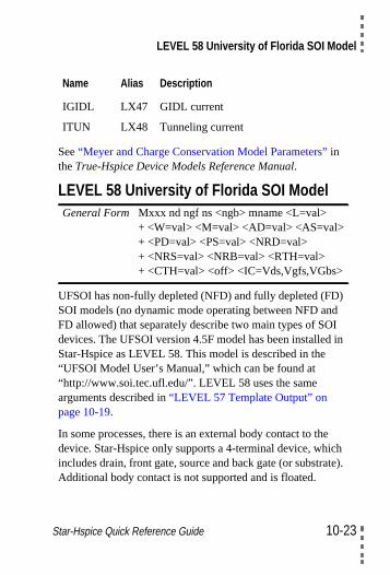
LEVEL 58 University of Florida SOI Model
dIin
he).
See“Meyer and Charge Conservation Model Parameters” intheTrue-Hspice Device Models Reference Manual.
LEVEL 58 University of Florida SOI Model
UFSOI has non-fully depleted (NFD) and fully depleted (FD)SOI models (no dynamic mode operating between NFD anFD allowed) that separately describe two main types of SOdevices. The UFSOI version 4.5F model has been installedStar-Hspice as LEVEL 58. This model is described in the“UFSOI Model User’s Manual,” which can be found at“http://www.soi.tec.ufl.edu/”. LEVEL 58 uses the samearguments described in“LEVEL 57 Template Output” onpage 10-19.
In some processes, there is an external body contact to thedevice. Star-Hspice only supports a 4-terminal device, whicincludes drain, front gate, source and back gate (or substratAdditional body contact is not supported and is floated.
IGIDL LX47 GIDL current
ITUN LX48 Tunneling current
General Form Mxxx nd ngf ns <ngb> mname <L=val>+ <W=val> <M=val> <AD=val> <AS=val>+ <PD=val> <PS=val> <NRD=val>+ <NRS=val> <NRB=val> <RTH=val>+ <CTH=val> <off> <IC=Vds,Vgfs,VGbs>
Name Alias Description
Star-Hspice Quick Reference Guide 10-23

MOSFET Models
e
e
The effects of parasitic diodes in SOI are different from thosin bulk MOSFET. The Star-Hspice junction model (ACM),developed for bulk MOSFETs, is not included in the SOImodel. For more information about this model, see“LEVEL58 University of Florida SOI Model”in theTrue-HspiceDevice Models Reference Manual.
Using the UFSOI Model in Star-Hspice• Default value for channel length L and width W is 1.0e-6.
• LEVEL 58 supports only 4 nodes (only floating-bodydevices). AB is usually zero and should be specified.
• When the self-heating option is activated, RTH and CTHdefine the thermal impedance of the device.
• For M > 1, W, AD, AS, NRD, NRS, NRB, PDJ, PSJ, RTH,and CTH must be specified per gate finger.
• The initial condition IC is in the order: drain voltage Vds,front gate voltage Vgfs, and back gate voltage Vbgs.
• The model line must include LEVEL=58 and NFDMOD=0for FD or NFDMOD=1 for NFD devices.
• Specifying VFBF turns off the narrow-width effect definedby NQFSW (positive or negative) and the reverse short-channel effect defined by LRSCE (and NBH or NHALO);the latter effect is also turned off when WKF is specified.
• For floating-body devices, set CGFBO=0.
• JRO and SEFF influence the gain of the BJT, but LDIFFaffects only bipolar charge storage in the source/drain. ThBJT gain is influenced by NBH and NHALO (if THALO isspecified) as well.
10-24 Star-Hspice Quick Reference Guide
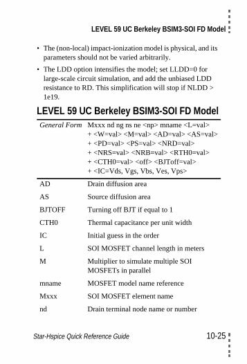
LEVEL 59 UC Berkeley BSIM3-SOI FD Model
• The (non-local) impact-ionization model is physical, and itsparameters should not be varied arbitrarily.
• The LDD option intensifies the model; set LLDD=0 forlarge-scale circuit simulation, and add the unbiased LDDresistance to RD. This simplification will stop if NLDD >1e19.
LEVEL 59 UC Berkeley BSIM3-SOI FD ModelGeneral Form Mxxx nd ng ns ne <np> mname <L=val>
+ <W=val> <M=val> <AD=val> <AS=val>+ <PD=val> <PS=val> <NRD=val>+ <NRS=val> <NRB=val> <RTH0=val>+ <CTH0=val> <off> <BJToff=val>+ <IC=Vds, Vgs, Vbs, Ves, Vps>
AD Drain diffusion area
AS Source diffusion area
BJTOFF Turning off BJT if equal to 1
CTH0 Thermal capacitance per unit width
IC Initial guess in the order
L SOI MOSFET channel length in meters
M Multiplier to simulate multiple SOIMOSFETs in parallel
mname MOSFET model name reference
Mxxx SOI MOSFET element name
nd Drain terminal node name or number
Star-Hspice Quick Reference Guide 10-25
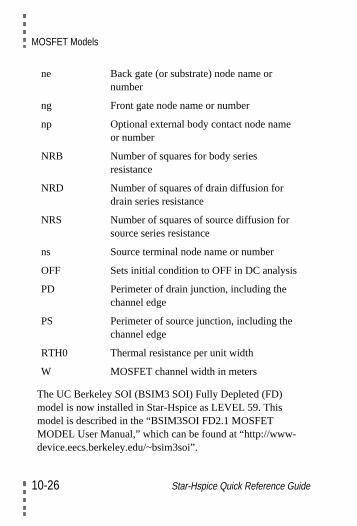
MOSFET Models
The UC Berkeley SOI (BSIM3 SOI) Fully Depleted (FD)model is now installed in Star-Hspice as LEVEL 59. Thismodel is described in the “BSIM3SOI FD2.1 MOSFETMODEL User Manual,” which can be found at “http://www-device.eecs.berkeley.edu/~bsim3soi”.
ne Back gate (or substrate) node name ornumber
ng Front gate node name or number
np Optional external body contact node nameor number
NRB Number of squares for body seriesresistance
NRD Number of squares of drain diffusion fordrain series resistance
NRS Number of squares of source diffusion forsource series resistance
ns Source terminal node name or number
OFF Sets initial condition to OFF in DC analysis
PD Perimeter of drain junction, including thechannel edge
PS Perimeter of source junction, including thechannel edge
RTH0 Thermal resistance per unit width
W MOSFET channel width in meters
10-26 Star-Hspice Quick Reference Guide
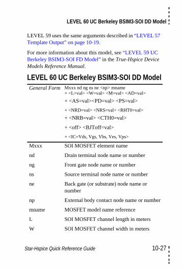
LEVEL 60 UC Berkeley BSIM3-SOI DD Model
r
LEVEL 59 uses the same arguments described in“LEVEL 57Template Output” on page 10-19.
For more information about this model, see“LEVEL 59 UCBerkeley BSIM3-SOI FD Model”in theTrue-Hspice DeviceModels Reference Manual.
LEVEL 60 UC Berkeley BSIM3-SOI DD ModelGeneral Form Mxxx nd ng ns ne <np> mname
+ <L=val> <W=val> <M=val> <AD=val>
+ <AS=val><PD=val> <PS=val>
+ <NRD=val> <NRS=val> <RHT0=val>
+ <NRB=val> <CTH0=val>
+ <off> <BJToff=val>
+ <IC=Vds, Vgs, Vbs, Ves, Vps>
Mxxx SOI MOSFET element name
nd Drain terminal node name or number
ng Front gate node name or number
ns Source terminal node name or number
ne Back gate (or substrate) node name ornumber
np External body contact node name or numbe
mname MOSFET model name reference
L SOI MOSFET channel length in meters
W SOI MOSFET channel width in meters
Star-Hspice Quick Reference Guide 10-27
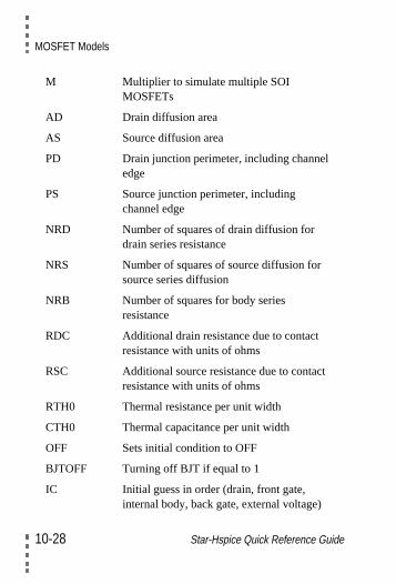
MOSFET Models
t
M Multiplier to simulate multiple SOIMOSFETs
AD Drain diffusion area
AS Source diffusion area
PD Drain junction perimeter, including channeledge
PS Source junction perimeter, includingchannel edge
NRD Number of squares of drain diffusion fordrain series resistance
NRS Number of squares of source diffusion forsource series diffusion
NRB Number of squares for body seriesresistance
RDC Additional drain resistance due to contactresistance with units of ohms
RSC Additional source resistance due to contacresistance with units of ohms
RTH0 Thermal resistance per unit width
CTH0 Thermal capacitance per unit width
OFF Sets initial condition to OFF
BJTOFF Turning off BJT if equal to 1
IC Initial guess in order (drain, front gate,internal body, back gate, external voltage)
10-28 Star-Hspice Quick Reference Guide
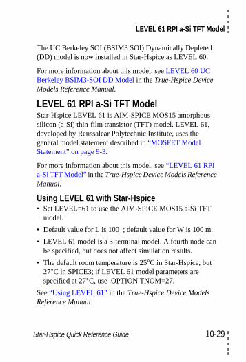
LEVEL 61 RPI a-Si TFT Model
The UC Berkeley SOI (BSIM3 SOI) Dynamically Depleted(DD) model is now installed in Star-Hspice as LEVEL 60.
For more information about this model, seeLEVEL 60 UCBerkeley BSIM3-SOI DD Model in theTrue-Hspice DeviceModels Reference Manual.
LEVEL 61 RPI a-Si TFT ModelStar-Hspice LEVEL 61 is AIM-SPICE MOS15 amorphoussilicon (a-Si) thin-film transistor (TFT) model. LEVEL 61,developed by Renssalear Polytechnic Institute, uses thegeneral model statement described in“MOSFET ModelStatement” on page 9-3.
For more information about this model, see“LEVEL 61 RPIa-Si TFT Model”in theTrue-Hspice Device Models ReferenceManual.
Using LEVEL 61 with Star-Hspice• Set LEVEL=61 to use the AIM-SPICE MOS15 a-Si TFT
model.
• Default value for L is 100 ; default value for W is 100 m.
• LEVEL 61 model is a 3-terminal model. A fourth node canbe specified, but does not affect simulation results.
• The default room temperature is 25°C in Star-Hspice, but27°C in SPICE3; if LEVEL 61 model parameters arespecified at 27°C, use .OPTION TNOM=27.
See“Using LEVEL 61” in theTrue-Hspice Device ModelsReference Manual.
Star-Hspice Quick Reference Guide 10-29
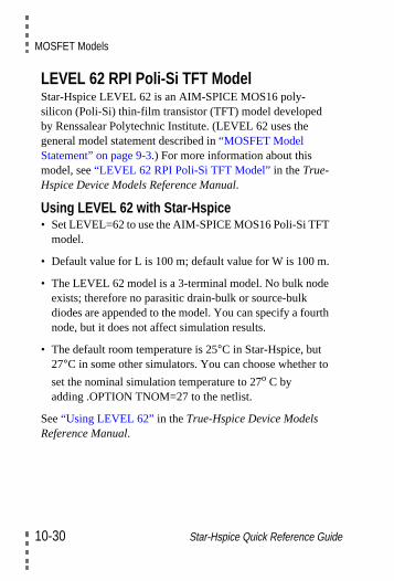
MOSFET Models
.
th
to
LEVEL 62 RPI Poli-Si TFT ModelStar-Hspice LEVEL 62 is an AIM-SPICE MOS16 poly-silicon (Poli-Si) thin-film transistor (TFT) model developedby Renssalear Polytechnic Institute. (LEVEL 62 uses thegeneral model statement described in“MOSFET ModelStatement” on page 9-3.) For more information about thismodel, see“LEVEL 62 RPI Poli-Si TFT Model” in theTrue-Hspice Device Models Reference Manual.
Using LEVEL 62 with Star-Hspice• Set LEVEL=62 to use the AIM-SPICE MOS16 Poli-Si TFT
model.
• Default value for L is 100 m; default value for W is 100 m
• The LEVEL 62 model is a 3-terminal model. No bulk nodeexists; therefore no parasitic drain-bulk or source-bulkdiodes are appended to the model. You can specify a fournode, but it does not affect simulation results.
• The default room temperature is 25°C in Star-Hspice, but27°C in some other simulators. You can choose whether
set the nominal simulation temperature to 27o C byadding .OPTION TNOM=27 to the netlist.
See“Using LEVEL 62” in theTrue-Hspice Device ModelsReference Manual.
10-30 Star-Hspice Quick Reference Guide
MOS Level 63, Philips MOS11 Model
l
,
l
7
eln
he
MOS Level 63, Philips MOS11 ModelThe Philips MOS Model 11, Level 1100, is available as Leve63 in Star-Hspice (based on the “Unclassified Report NL-UR2001/813” by R. Langevelde). And for parasitic diode modelthe Philips JUNCAP Parasitic Diode Model is available.
For additional information regarding the MOS Model 11 andthe Philips JUNCAP Parasitic Diode Model, see:
http://www.semiconductors.philips.com/Philips_Models
Using the Philips MOS11 Model in Star-Hspice1. Set Level=63 to identify the model as Philips MOS Mode
11
2. The default room temperature is 25 in Star-Hspice, but is 2in most other simulators. When comparing to othersimulators, set the simulation temperature to 27,using .TEMP 27 or .OPTIONS TNOM=27.
3. The model parameter set should always include the modreference temperature, TR, which corresponds to TREF iother levels in Star-Hspice. The default for TR is 21.0, tomatch the Philips simulator.
4. The model has its own charge-based capacitance model. TCAPOP parameter, which selects different capacitancemodels, is ignored in this model.
5. The model uses the analytical derivatives for theconductances. The DERIV parameter, which selects thefinite difference method, is ignored in this model
Star-Hspice Quick Reference Guide 10-31
MOSFET Models
nt
atrs
hen
6. DTEMP can be used with this model. It is set on the elemeline and increases the temperature of individual elementsrelative to the circuit temperature.
7. Since defaults are nonzero, it is strongly recommended thevery model parameter listed in Level 63 Model Parametetable be set in the .MODEL statement.
8. The general syntax for MOSFET element is the same as tother standard MOSFET models other than PS and PD. ILevel=63, PS and PD are defined as the length of thesidewall of the source/drain which is not under the gate
9. MOS11 has LMIN as its own parameter, which has thedifference definition from that of Star-Hspice. To avoid theconflict with LMIN in Star-Hspice, LMIN parameter inHSPICE level=63 was changed to LLMIN.
10-32 Star-Hspice Quick Reference Guide
Star-Hspice Quic
11-
Chapter 11Behavior Macromodeling
r
The topics covered in this chapter are:
• Subcircuit/Macros
• Voltage and Current Controlled Elements
Star-Hspice performs the following types of behavioralmodeling.
Subcircuit/Macros.SUBCKT or .MACRO Statement
See“.SUBCKT or .MACRO Statement” in theStar-HspiceManual.
General Form .SUBCKT subnam n1 <n2 n3 …>+ <parnam=val …>
Or .MACRO subnam n1 <n2 n3 …>+ <parnam=val …>
n1 … Node name for external reference
parnam A parameter name set to a value or anotheparameter
subnam Reference name for the subcircuit modelcall
k Reference Guide 11-1
Behavior Macromodeling
y
.ENDS or .EOM Statement
See“.ENDS or .EOM Statement” in theStar-Hspice Manual.
Subcircuit Calls
See“Subcircuit Call Statement” in theStar-Hspice Manual.
Voltage and Current Controlled ElementsStar-Hspice supports the following voltage and currentcontrolled elements. For detailed information, see“UsingVoltage and Current Controlled Elements”in theStar-HspiceManual.
General Form .ENDS <SUBNAM>
Or .EOM <SUBNAM>
General Form Xyyy n1 <n2 n3 …> subnam+ <parnam=val …> <M=val>
M Multiplier
n1 … Node names for external reference
parnam A parameter name set to a value for use onlin the subcircuit
subnam Subcircuit model reference name
Xyyy Subcircuit element name
11-2 Star-Hspice Quick Reference Guide
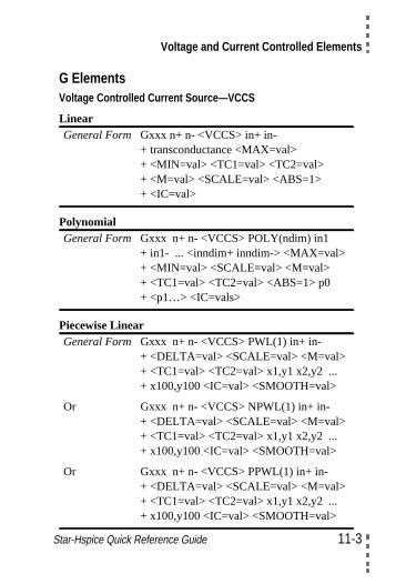
Voltage and Current Controlled Elements
Star-Hspice Quick Reference Guide 11-3
G ElementsVoltage Controlled Current Source—VCCS
Linear
Polynomial
Piecewise Linear
General Form Gxxx n+ n- <VCCS> in+ in-+ transconductance <MAX=val>+ <MIN=val> <TC1=val> <TC2=val>+ <M=val> <SCALE=val> <ABS=1>+ <IC=val>
General Form Gxxx n+ n- <VCCS> POLY(ndim) in1+ in1- ... <inndim+ inndim-> <MAX=val>+ <MIN=val> <SCALE=val> <M=val>+ <TC1=val> <TC2=val> <ABS=1> p0+ <p1…> <IC=vals>
General Form
Or
Or
Gxxx n+ n- <VCCS> PWL(1) in+ in-+ <DELTA=val> <SCALE=val> <M=val>+ <TC1=val> <TC2=val> x1,y1 x2,y2 ...+ x100,y100 <IC=val> <SMOOTH=val>
Gxxx n+ n- <VCCS> NPWL(1) in+ in-+ <DELTA=val> <SCALE=val> <M=val>+ <TC1=val> <TC2=val> x1,y1 x2,y2 ...+ x100,y100 <IC=val> <SMOOTH=val>
Gxxx n+ n- <VCCS> PPWL(1) in+ in-+ <DELTA=val> <SCALE=val> <M=val>+ <TC1=val> <TC2=val> x1,y1 x2,y2 ...+ x100,y100 <IC=val> <SMOOTH=val>
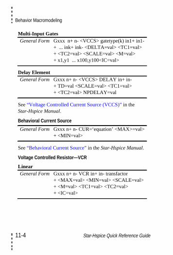
Behavior Macromodeling
Multi-Input Gates
Delay Element
See“Voltage Controlled Current Source (VCCS)” in theStar-Hspice Manual.
Behavioral Current Source
See“Behavioral Current Source” in theStar-Hspice Manual.
Voltage Controlled Resistor—VCR
Linear
General Form Gxxx n+ n- <VCCS> gatetype(k) in1+ in1-+ ... ink+ ink- <DELTA=val> <TC1=val>+ <TC2=val> <SCALE=val> <M=val>+ x1,y1 ... x100,y100<IC=val>
General Form Gxxx n+ n- <VCCS> DELAY in+ in-+ TD=val <SCALE=val> <TC1=val>+ <TC2=val> NPDELAY=val
General Form Gxxx n+ n- CUR=‘equation’ <MAX>=val>+ <MIN=val>
General Form Gxxx n+ n- VCR in+ in- transfactor+ <MAX=val> <MIN=val> <SCALE=val>+ <M=val> <TC1=val> <TC2=val>+ <IC=val>
11-4 Star-Hspice Quick Reference Guide
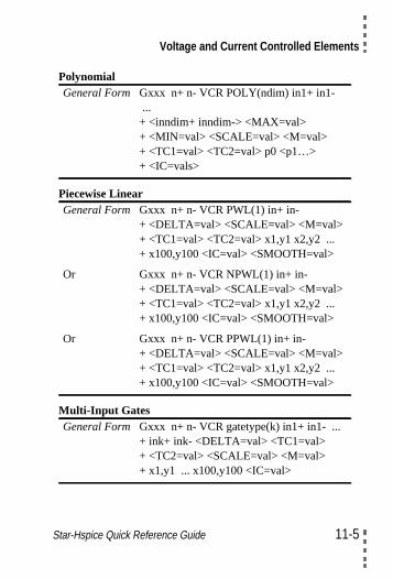
Voltage and Current Controlled Elements
Polynomial
Piecewise Linear
Multi-Input Gates
General Form Gxxx n+ n- VCR POLY(ndim) in1+ in1-...+ <inndim+ inndim-> <MAX=val>+ <MIN=val> <SCALE=val> <M=val>+ <TC1=val> <TC2=val> p0 <p1…>+ <IC=vals>
General Form
Or
Or
Gxxx n+ n- VCR PWL(1) in+ in-+ <DELTA=val> <SCALE=val> <M=val>+ <TC1=val> <TC2=val> x1,y1 x2,y2 ...+ x100,y100 <IC=val> <SMOOTH=val>
Gxxx n+ n- VCR NPWL(1) in+ in-+ <DELTA=val> <SCALE=val> <M=val>+ <TC1=val> <TC2=val> x1,y1 x2,y2 ...+ x100,y100 <IC=val> <SMOOTH=val>
Gxxx n+ n- VCR PPWL(1) in+ in-+ <DELTA=val> <SCALE=val> <M=val>+ <TC1=val> <TC2=val> x1,y1 x2,y2 ...+ x100,y100 <IC=val> <SMOOTH=val>
General Form Gxxx n+ n- VCR gatetype(k) in1+ in1- ...+ ink+ ink- <DELTA=val> <TC1=val>+ <TC2=val> <SCALE=val> <M=val>+ x1,y1 ... x100,y100 <IC=val>
Star-Hspice Quick Reference Guide 11-5
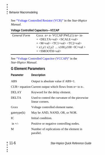
Behavior Macromodeling
See“Voltage Controlled Resistor (VCR)” in theStar-HspiceManual.
Voltage Controlled Capacitors—VCCAP
See“Voltage Controlled Capacitor (VCCAP)” in theStar-Hspice Manual.
G Element Parameters
General Form Gxxx n+ n- VCCAP PWL(1) in+ in-+ <DELTA=val> <SCALE=val>+ <M=val> <TC1=val> <TC2=val>+ x1,y1 x2,y2 ... x100,y100 <IC=val >+ <SMOOTH=val>
Parameter Description
ABS Output is absolute value if ABS=1.
CUR= equation Current output which flows from n+ to n-.
DELAY Keyword for the delay element.
DELTA Used to control the curvature of the piecewiselinear corners.
Gxxx Voltage controlled element name.
gatetype(k) May be AND, NAND, OR, or NOR.
IC Initial condition.
in +/- Positive or negative controlling nodes.
M Number of replications of the element inparallel.
11-6 Star-Hspice Quick Reference Guide

Voltage and Current Controlled Elements
MAX Maximum current or resistance value.
MIN Minimum current or resistance value.
n+/- Positive or negative node of controlledelement.
NPDELAY Sets the number of data points to be used indelay simulations.
NPWL Models the symmetrical bidirectional switchor transfer gate, NMOS.
p0, p1 … Polynomial coefficients.
POLY Polynomial dimension.
PWL Piecewise linear function keyword.
PPWL Models the symmetrical bidirectional switchor transfer gate, PMOS.
SCALE Element value multiplier.
SMOOTH For piecewise linear dependent sourceelements, SMOOTH selects the curvesmoothing method.
TC1,TC2 First-order and second-order temperaturecoefficients.
TD Time delay keyword.
transconduct-ance
Voltage to current conversion factor.
Parameter Description
Star-Hspice Quick Reference Guide 11-7
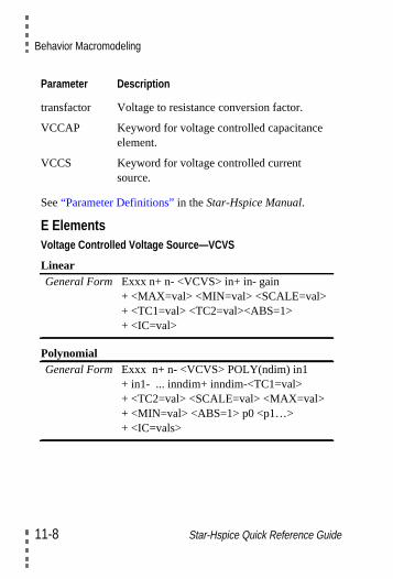
Behavior Macromodeling
See“Parameter Definitions” in theStar-Hspice Manual.
E ElementsVoltage Controlled Voltage Source—VCVS
Linear
Polynomial
transfactor Voltage to resistance conversion factor.
VCCAP Keyword for voltage controlled capacitanceelement.
VCCS Keyword for voltage controlled currentsource.
General Form Exxx n+ n- <VCVS> in+ in- gain+ <MAX=val> <MIN=val> <SCALE=val>+ <TC1=val> <TC2=val><ABS=1>+ <IC=val>
General Form Exxx n+ n- <VCVS> POLY(ndim) in1+ in1- ... inndim+ inndim-<TC1=val>+ <TC2=val> <SCALE=val> <MAX=val>+ <MIN=val> <ABS=1> p0 <p1…>+ <IC=vals>
Parameter Description
11-8 Star-Hspice Quick Reference Guide
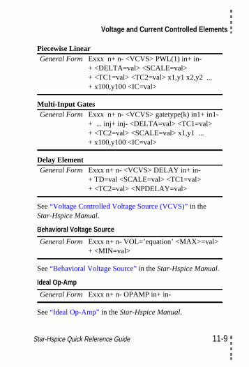
Voltage and Current Controlled Elements
Piecewise Linear
Multi-Input Gates
Delay Element
See“Voltage Controlled Voltage Source (VCVS)” in theStar-Hspice Manual.
Behavioral Voltage Source
See“Behavioral Voltage Source” in theStar-Hspice Manual.
Ideal Op-Amp
See“Ideal Op-Amp” in theStar-Hspice Manual.
General Form Exxx n+ n- <VCVS> PWL(1) in+ in-+ <DELTA=val> <SCALE=val>+ <TC1=val> <TC2=val> x1,y1 x2,y2 ...+ x100,y100 <IC=val>
General Form Exxx n+ n- <VCVS> gatetype(k) in1+ in1-+ ... inj+ inj- <DELTA=val> <TC1=val>+ <TC2=val> <SCALE=val> x1,y1 ...+ x100,y100 <IC=val>
General Form Exxx n+ n- <VCVS> DELAY in+ in-+ TD=val <SCALE=val> <TC1=val>+ <TC2=val> <NPDELAY=val>
General Form Exxx n+ n- VOL=’equation’ <MAX>=val>+ <MIN=val>
General Form Exxx n+ n- OPAMP in+ in-
Star-Hspice Quick Reference Guide 11-9
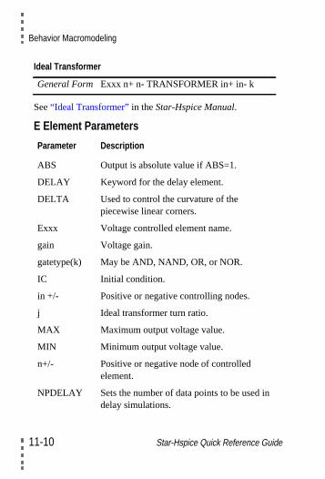
Behavior Macromodeling
Ideal Transformer
See“Ideal Transformer” in theStar-Hspice Manual.
E Element Parameters
General Form Exxx n+ n- TRANSFORMER in+ in- k
Parameter Description
ABS Output is absolute value if ABS=1.
DELAY Keyword for the delay element.
DELTA Used to control the curvature of thepiecewise linear corners.
Exxx Voltage controlled element name.
gain Voltage gain.
gatetype(k) May be AND, NAND, OR, or NOR.
IC Initial condition.
in +/- Positive or negative controlling nodes.
j Ideal transformer turn ratio.
MAX Maximum output voltage value.
MIN Minimum output voltage value.
n+/- Positive or negative node of controlledelement.
NPDELAY Sets the number of data points to be used indelay simulations.
11-10 Star-Hspice Quick Reference Guide
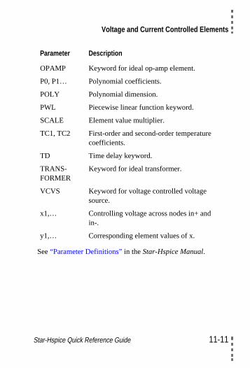
Voltage and Current Controlled Elements
See“Parameter Definitions” in theStar-Hspice Manual.
OPAMP Keyword for ideal op-amp element.
P0, P1… Polynomial coefficients.
POLY Polynomial dimension.
PWL Piecewise linear function keyword.
SCALE Element value multiplier.
TC1, TC2 First-order and second-order temperaturecoefficients.
TD Time delay keyword.
TRANS-FORMER
Keyword for ideal transformer.
VCVS Keyword for voltage controlled voltagesource.
x1,… Controlling voltage across nodes in+ andin-.
y1,… Corresponding element values of x.
Parameter Description
Star-Hspice Quick Reference Guide 11-11
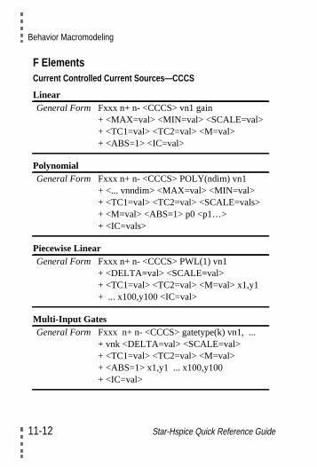
Behavior Macromodeling
F ElementsCurrent Controlled Current Sources—CCCS
Linear
Polynomial
Piecewise Linear
Multi-Input Gates
General Form Fxxx n+ n- <CCCS> vn1 gain+ <MAX=val> <MIN=val> <SCALE=val>+ <TC1=val> <TC2=val> <M=val>+ <ABS=1> <IC=val>
General Form Fxxx n+ n- <CCCS> POLY(ndim) vn1+ <... vnndim> <MAX=val> <MIN=val>+ <TC1=val> <TC2=val> <SCALE=vals>+ <M=val> <ABS=1> p0 <p1…>+ <IC=vals>
General Form Fxxx n+ n- <CCCS> PWL(1) vn1+ <DELTA=val> <SCALE=val>+ <TC1=val> <TC2=val> <M=val> x1,y1+ ... x100,y100 <IC=val>
General Form Fxxx n+ n- <CCCS> gatetype(k) vn1, ...+ vnk <DELTA=val> <SCALE=val>+ <TC1=val> <TC2=val> <M=val>+ <ABS=1> x1,y1 ... x100,y100+ <IC=val>
11-12 Star-Hspice Quick Reference Guide
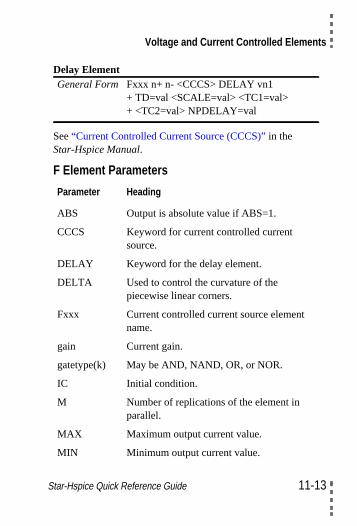
Voltage and Current Controlled Elements
Delay Element
See“Current Controlled Current Source (CCCS)” in theStar-Hspice Manual.
F Element Parameters
General Form Fxxx n+ n- <CCCS> DELAY vn1+ TD=val <SCALE=val> <TC1=val>+ <TC2=val> NPDELAY=val
Parameter Heading
ABS Output is absolute value if ABS=1.
CCCS Keyword for current controlled currentsource.
DELAY Keyword for the delay element.
DELTA Used to control the curvature of thepiecewise linear corners.
Fxxx Current controlled current source elementname.
gain Current gain.
gatetype(k) May be AND, NAND, OR, or NOR.
IC Initial condition.
M Number of replications of the element inparallel.
MAX Maximum output current value.
MIN Minimum output current value.
Star-Hspice Quick Reference Guide 11-13
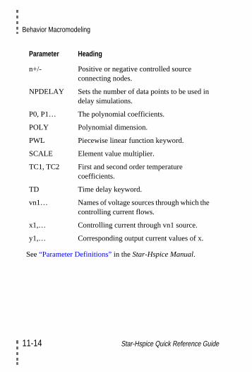
Behavior Macromodeling
See“Parameter Definitions” in theStar-Hspice Manual.
n+/- Positive or negative controlled sourceconnecting nodes.
NPDELAY Sets the number of data points to be used indelay simulations.
P0, P1… The polynomial coefficients.
POLY Polynomial dimension.
PWL Piecewise linear function keyword.
SCALE Element value multiplier.
TC1, TC2 First and second order temperaturecoefficients.
TD Time delay keyword.
vn1… Names of voltage sources through which thecontrolling current flows.
x1,… Controlling current through vn1 source.
y1,… Corresponding output current values of x.
Parameter Heading
11-14 Star-Hspice Quick Reference Guide
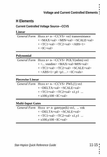
Voltage and Current Controlled Elements
H ElementsCurrent Controlled Voltage Source—CCVS
Linear
Polynomial
Piecewise Linear
Multi-Input Gates
General Form Hxxx n+ n- <CCVS> vn1 transresistance+ <MAX=val> <MIN=val> <SCALE=val>+ <TC1=val> <TC2=val> <ABS=1>+ <IC=val>
General Form Hxxx n+ n- <CCVS> POLY(ndim) vn1+ <... vnndim> <MAX=val>MIN=val>+ <TC1=val> <TC2=val> <SCALE=val>+ <ABS=1> p0 <p1…> <IC=vals>
General Form Hxxx n+ n- <CCVS> PWL(1) vn1+ <DELTA=val> <SCALE=val>+ <TC1=val> <TC2=val> x1,y1 ...+ x100,y100 <IC=val>
General Form Hxxx n+ n- gatetype(k) vn1, ... vnk+ <DELTA=val> <SCALE=val>+ <TC1=val> <TC2=val> x1,y1 ...+ x100,y100 <IC=val>
Star-Hspice Quick Reference Guide 11-15
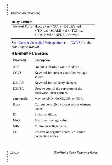
Behavior Macromodeling
Delay Element
See“Current Controlled Voltage Source — (CCVS)” in theStar-Hspice Manual.
H Element Parameters
General Form Hxxx n+ n- <CCVS> DELAY vn1+ TD=val <SCALE=val> <TC1=val>+ <TC2=val> <NPDELAY=val>
Parameter Description
ABS Output is absolute value if ABS=1.
CCVS Keyword for current controlled voltagesource.
DELAY Keyword for the delay element.
DELTA Used to control the curvature of thepiecewise linear corners.
gatetype(k) May be AND, NAND, OR, or NOR.
Hxxx Current controlled voltage source elementname.
IC Initial condition.
MAX Maximum voltage value.
MIN Minimum voltage value.
n+/- Positive or negative controlled sourceconnecting nodes.
11-16 Star-Hspice Quick Reference Guide
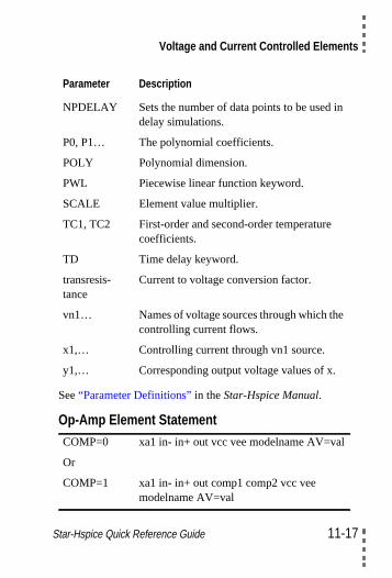
Voltage and Current Controlled Elements
See“Parameter Definitions” in theStar-Hspice Manual.
Op-Amp Element Statement
NPDELAY Sets the number of data points to be used indelay simulations.
P0, P1… The polynomial coefficients.
POLY Polynomial dimension.
PWL Piecewise linear function keyword.
SCALE Element value multiplier.
TC1, TC2 First-order and second-order temperaturecoefficients.
TD Time delay keyword.
transresis-tance
Current to voltage conversion factor.
vn1… Names of voltage sources through which thecontrolling current flows.
x1,… Controlling current through vn1 source.
y1,… Corresponding output voltage values of x.
COMP=0 xa1 in- in+ out vcc vee modelname AV=val
Or
COMP=1 xa1 in- in+ out comp1 comp2 vcc veemodelname AV=val
Parameter Description
Star-Hspice Quick Reference Guide 11-17
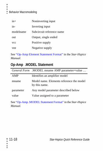
Behavior Macromodeling
el
See“Op-Amp Element Statement Format”in theStar-HspiceManual.
Op-Amp .MODEL Statement
See“Op-Amp .MODEL Statement Format”in theStar-HspiceManual.
in+ Noninverting input
in- Inverting input
modelname Subcircuit reference name
out Output, single ended
vcc Positive supply
vee Negative supply
General Form .MODEL mname AMP parameter=value …
AMP Identifies an amplifier model
mname Model name. Elements reference the modby this name.
parameter Any model parameter described below
value Value assigned to a parameter
11-18 Star-Hspice Quick Reference Guide
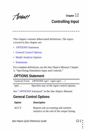
Star-Hspice Quic
12-
Chapter 12Controlling Input
This chapter contains abbreviated definitions. The topicscovered in this chapter are:
• .OPTIONS Statement
• General Control Options
• Model Analysis Options
• Statements
For complete definitions, see theStar-Hspice Manual, Chapter3, “Specifying Simulation Input and Controls.”
.OPTIONS Statement
See“.OPTIONS Statement” in theStar-Hspice Manual.
General Control Options
General Form .OPTIONS opt1 <opt2 opt3 …>
opt1 … Specifies any of the input control options.
Option Description
ACCT Reports job accounting and runtimestatistics at the end of the output listing.
k Reference Guide 12-1
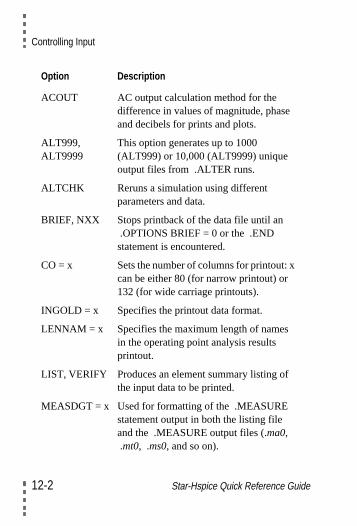
Controlling Input
ACOUT AC output calculation method for thedifference in values of magnitude, phaseand decibels for prints and plots.
ALT999,ALT9999
This option generates up to 1000(ALT999) or 10,000 (ALT9999) uniqueoutput files from .ALTER runs.
ALTCHK Reruns a simulation using differentparameters and data.
BRIEF, NXX Stops printback of the data file until an.OPTIONS BRIEF = 0 or the .ENDstatement is encountered.
CO = x Sets the number of columns for printout: xcan be either 80 (for narrow printout) or132 (for wide carriage printouts).
INGOLD = x Specifies the printout data format.
LENNAM = x Specifies the maximum length of namesin the operating point analysis resultsprintout.
LIST, VERIFY Produces an element summary listing ofthe input data to be printed.
MEASDGT = x Used for formatting of the .MEASUREstatement output in both the listing fileand the .MEASURE output files (.ma0,.mt0, .ms0, and so on).
Option Description
12-2 Star-Hspice Quick Reference Guide
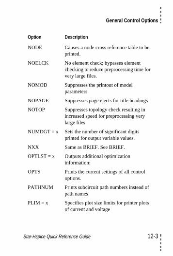
General Control Options
e
NODE Causes a node cross reference table to bprinted.NOELCK No element check; bypasses elementchecking to reduce preprocessing time forvery large files.
NOMOD Suppresses the printout of modelparameters
NOPAGE Suppresses page ejects for title headings
NOTOP Suppresses topology check resulting inincreased speed for preprocessing verylarge files
NUMDGT = x Sets the number of significant digitsprinted for output variable values.
NXX Same as BRIEF. See BRIEF.
OPTLST = x Outputs additional optimizationinformation:
OPTS Prints the current settings of all controloptions.
PATHNUM Prints subcircuit path numbers instead ofpath names
PLIM = x Specifies plot size limits for printer plotsof current and voltage
Option Description
Star-Hspice Quick Reference Guide 12-3
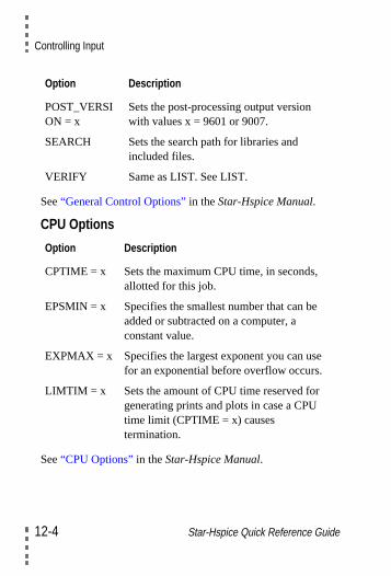
Controlling Input
See“General Control Options” in theStar-Hspice Manual.
CPU Options
See“CPU Options” in theStar-Hspice Manual.
POST_VERSION = x
Sets the post-processing output versionwith values x = 9601 or 9007.
SEARCH Sets the search path for libraries andincluded files.
VERIFY Same as LIST. See LIST.
Option Description
CPTIME = x Sets the maximum CPU time, in seconds,allotted for this job.
EPSMIN = x Specifies the smallest number that can beadded or subtracted on a computer, aconstant value.
EXPMAX = x Specifies the largest exponent you can usefor an exponential before overflow occurs.
LIMTIM = x Sets the amount of CPU time reserved forgenerating prints and plots in case a CPUtime limit (CPTIME = x) causestermination.
Option Description
12-4 Star-Hspice Quick Reference Guide
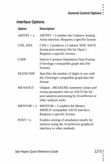
General Control Options
Interface Options
Option Description
ARTIST = x ARTIST = 2 enables the Cadence AnalogArtist interface. Requires a specific license.
CDS, SDA CDS = 2 produces a Cadence WSF ASCIIformat post-analysis file for Opus.Requires a specific license.
CSDF Selects Common Simulation Data Format(Viewlogic-compatible graph data fileformat).
DLENCSDF Specifies the number of digits to use withthe Viewlogic-compatible graph data fileformat.
MEASOUT Outputs .MEASURE statement values andsweep parameters into an ASCII file forpost-analysis processing by AvanWaves orother analysis tools.
MENTOR = x MENTOR = 2 enables the MentorMSPICE-compatible ASCII interface.Requires a specific license.
POST = x Enables storing of simulation results foranalysis using the AvanWaves graphicalinterface or other methods.
Star-Hspice Quick Reference Guide 12-5
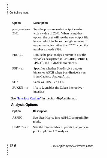
Controlling Input
See“Interface Options” in theStar-Hspice Manual.
Analysis Options
post_version=2001
Sets the post-processing output versionwith a value of 2001. When using thisoption, the user will see the new output fileheader which includes the right number ofoutput variables rather than **** when thenumber exceeds 9999.
PROBE Limits the post-analysis output to just thevariables designated in .PROBE, .PRINT,.PLOT, and .GRAPH statements.
PSF = x Specifies whether Star-Hspice outputsbinary or ASCII when Star-Hspice is runfrom Cadence Analog Artist.
SDA Same as CDS. See CDS.
ZUKEN = x If x is 2, enables the Zuken interactiveinterface.
Option Description
ASPEC Sets Star-Hspice into ASPEC compatibilitymode.
LIMPTS = x Sets the total number of points that you canprint or plot in AC analysis.
Option Description
12-6 Star-Hspice Quick Reference Guide
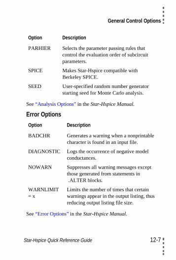
General Control Options
t
See“Analysis Options” in theStar-Hspice Manual.
Error Options
See“Error Options” in theStar-Hspice Manual.
PARHIER Selects the parameter passing rules thatcontrol the evaluation order of subcircuitparameters.
SPICE Makes Star-Hspice compatible withBerkeley SPICE.
SEED User-specified random number generatorstarting seed for Monte Carlo analysis.
Option Description
BADCHR Generates a warning when a nonprintablecharacter is found in an input file.
DIAGNOSTIC Logs the occurrence of negative modelconductances.
NOWARN Suppresses all warning messages excepthose generated from statements in.ALTER blocks.
WARNLIMIT= x
Limits the number of times that certainwarnings appear in the output listing, thusreducing output listing file size.
Option Description
Star-Hspice Quick Reference Guide 12-7

Controlling Input
r.
Version Options
See“Version Options” in theStar-Hspice Manual.
Model Analysis OptionsSee“Model Analysis Options” in theStar-Hspice Manual.
General Options
See“General Options” in theStar-Hspice Manual.
Option Description
H9007 Sets general control option default values tocorrespond to the values for Star-HspiceRelease H9007D.
Option Description
DCAP The DCAP option selects the equations usedin calculating the depletion capacitance forLEVEL 1 and 3 diodes and BJTs.
hier_scale Defines how Star-Hspice interprets theSparameter, either as a user-definedparameter or a Star-Hspice scale paramete
SCALE Element scaling factor.
TNOM The reference temperature for thesimulation.
12-8 Star-Hspice Quick Reference Guide
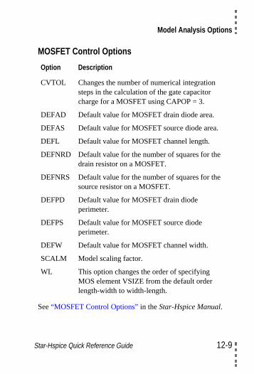
Model Analysis Options
MOSFET Control Options
See“MOSFET Control Options” in theStar-Hspice Manual.
Option Description
CVTOL Changes the number of numerical integrationsteps in the calculation of the gate capacitorcharge for a MOSFET using CAPOP = 3.
DEFAD Default value for MOSFET drain diode area.
DEFAS Default value for MOSFET source diode area.
DEFL Default value for MOSFET channel length.
DEFNRD Default value for the number of squares for thedrain resistor on a MOSFET.
DEFNRS Default value for the number of squares for thesource resistor on a MOSFET.
DEFPD Default value for MOSFET drain diodeperimeter.
DEFPS Default value for MOSFET source diodeperimeter.
DEFW Default value for MOSFET channel width.
SCALM Model scaling factor.
WL This option changes the order of specifyingMOS element VSIZE from the default orderlength-width to width-length.
Star-Hspice Quick Reference Guide 12-9

Controlling Input
DC Solution Control Options
Option Description
ABSH = x Sets the absolute current change throughvoltage defined branches (voltage sourcesand inductors).
ABSI = x Sets the absolute branch current errortolerance in diodes, BJTs, and JFETsduring DC and transient analysis.
ABSMOS = x Current error tolerance used for MOSFETdevices in both DC and transient analysis.
ABSTOL = x Sets the absolute node voltage errortolerance for DC and transient analysis.
ABSVDC = x Sets the absolute minimum voltage for DCand transient analysis.
DI = x Sets the maximum iteration-to-iterationcurrent change through voltage definedbranches (voltage sources and inductors).
KCLTEST Activates the KCL test (Kirchhoff’sCurrent Law) function.
MAXAMP = x Sets the maximum current through voltagedefined branches (voltage sources andinductors).
RELH = x Sets relative current tolerance throughvoltage defined branches (voltage sourcesand inductors).
12-10 Star-Hspice Quick Reference Guide
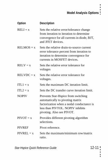
Model Analysis Options
RELI = x Sets the relative error/tolerance changefrom iteration to iteration to determineconvergence for all currents in diode, BJT,and JFET devices.
RELMOS = x Sets the relative drain-to-source currenterror tolerance percent from iteration toiteration to determine convergence forcurrents in MOSFET devices.
RELV = x Sets the relative error tolerance forvoltages
RELVDC = x Sets the relative error tolerance forvoltages.
ITL1 = x Sets the maximum DC iteration limit.
ITL2 = x Sets the DC transfer curve iteration limit.
NOPIV Prevents Star-Hspice from switchingautomatically to pivoting matrixfactorization when a nodal conductance isless than PIVTOL. NOPIV inhibitspivoting. Also see PIVOT.
PIVOT = x Provides different pivoting algorithmselections.
PIVREF Pivot reference.
PIVREL = x Sets the maximum/minimum row/matrixratio.
Option Description
Star-Hspice Quick Reference Guide 12-11
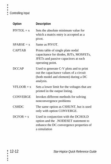
Controlling Input
PIVTOL = x Sets the absolute minimum value forwhich a matrix entry is accepted as apivot.
SPARSE = x Same as PIVOT.
CAPTAB Prints table of single plate nodalcapacitance for diodes, BJTs, MOSFETs,JFETs and passive capacitors at eachoperating point.
DCCAP Used to generate C-V plots and to printout the capacitance values of a circuit(both model and element) during a DCanalysis.
VFLOOR = x Sets a lower limit for the voltages that areprinted in the output listing.
CONVERGE Invokes different methods for solvingnonconvergence problems
CSHDC The same option as CSHUNT, but is usedonly with option CONVERGE.
DCFOR = x Used in conjunction with the DCHOLDoption and the .NODESET statement toenhance the DC convergence properties ofa simulation
Option Description
12-12 Star-Hspice Quick Reference Guide
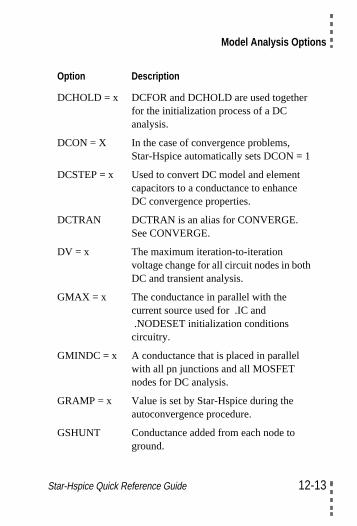
Model Analysis Options
DCHOLD = x DCFOR and DCHOLD are used togetherfor the initialization process of a DCanalysis.
DCON = X In the case of convergence problems,Star-Hspice automatically sets DCON = 1
DCSTEP = x Used to convert DC model and elementcapacitors to a conductance to enhanceDC convergence properties.
DCTRAN DCTRAN is an alias for CONVERGE.See CONVERGE.
DV = x The maximum iteration-to-iterationvoltage change for all circuit nodes in bothDC and transient analysis.
GMAX = x The conductance in parallel with thecurrent source used for .IC and.NODESET initialization conditionscircuitry.
GMINDC = x A conductance that is placed in parallelwith all pn junctions and all MOSFETnodes for DC analysis.
GRAMP = x Value is set by Star-Hspice during theautoconvergence procedure.
GSHUNT Conductance added from each node toground.
Option Description
Star-Hspice Quick Reference Guide 12-13
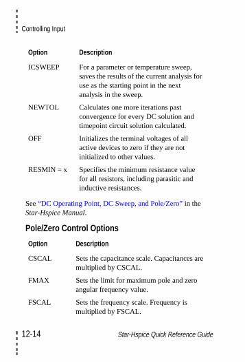
Controlling Input
re
See“DC Operating Point, DC Sweep, and Pole/Zero” in theStar-Hspice Manual.
Pole/Zero Control Options
ICSWEEP For a parameter or temperature sweep,saves the results of the current analysis foruse as the starting point in the nextanalysis in the sweep.
NEWTOL Calculates one more iterations pastconvergence for every DC solution andtimepoint circuit solution calculated.
OFF Initializes the terminal voltages of allactive devices to zero if they are notinitialized to other values.
RESMIN = x Specifies the minimum resistance valuefor all resistors, including parasitic andinductive resistances.
Option Description
CSCAL Sets the capacitance scale. Capacitances amultiplied by CSCAL.
FMAX Sets the limit for maximum pole and zeroangular frequency value.
FSCAL Sets the frequency scale. Frequency ismultiplied by FSCAL.
Option Description
12-14 Star-Hspice Quick Reference Guide
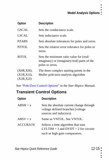
Model Analysis Options
s.
r
See“Pole/Zero Control Options” in theStar-Hspice Manual.
Transient Control Options
GSCAL Sets the conductance scale.
LSCAL Sets inductance scale.
PZABS Sets absolute tolerances for poles and zero
PZTOL Sets the relative error tolerance for poles ozeros.
RITOL Sets the minimum ratio value for (real/imaginary) or (imaginary/real) parts of thepoles or zeros.
(X0R,X0I),(X1R,X1I),(X2R,X2I)
The three complex starting points in theMuller pole/zero analysis algorithm
Option Description
ABSH = x Sets the absolute current change throughvoltage defined branches (voltagesources and inductors).
ABSV = x Same as VNTOL. See VNTOL.
ACCURATE Selects a time algorithm that usesLVLTIM = 3 and DVDT = 2 for circuits
such as high-gain comparators.
Option Description
Star-Hspice Quick Reference Guide 12-15
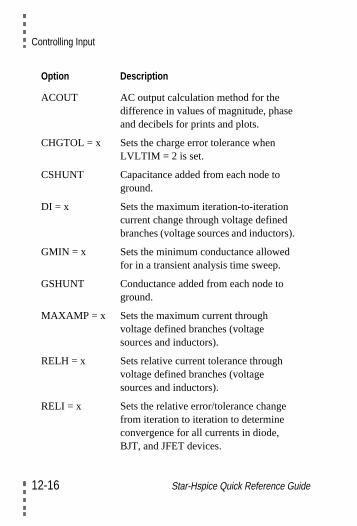
Controlling Input
ACOUT AC output calculation method for thedifference in values of magnitude, phaseand decibels for prints and plots.
CHGTOL = x Sets the charge error tolerance whenLVLTIM = 2 is set.
CSHUNT Capacitance added from each node toground.
DI = x Sets the maximum iteration-to-iterationcurrent change through voltage definedbranches (voltage sources and inductors).
GMIN = x Sets the minimum conductance allowedfor in a transient analysis time sweep.
GSHUNT Conductance added from each node toground.
MAXAMP = x Sets the maximum current throughvoltage defined branches (voltagesources and inductors).
RELH = x Sets relative current tolerance throughvoltage defined branches (voltagesources and inductors).
RELI = x Sets the relative error/tolerance changefrom iteration to iteration to determineconvergence for all currents in diode,BJT, and JFET devices.
Option Description
12-16 Star-Hspice Quick Reference Guide
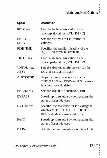
Model Analysis Options
RELQ = x Used in the local truncation errortimestep algorithm (LVLTIM = 2).
RELTOL,RELV
Sets the relative error tolerance forvoltages
RISETIME Specifies the smallest risetime of thesignal, .OPTION RISETIME = x.
TRTOL = x Used in the local truncation errortimestep algorithm (LVLTIM = 2)
VNTOL = x,ABSV
Sets the absolute minimum voltage forDC and transient analysis.
AUTOSTOP Stops the transient analysis when allTRIG-TARG and FIND-WHEN measurefunctions are calculated.
BKPSIZ = x Sets the size of the breakpoint table.
BYPASS Speeds up simulation by not updating thestatus of latent devices.
BYTOL = x Specifies the tolerance for the voltage atwhich a MOSFET, MESFET, JFET,BJT, or diode is considered latent.
FAST Speeds up simulation by not updating thestatus of latent devices.
ITLPZ Sets the pole/zero analysis iteration limit.
Option Description
Star-Hspice Quick Reference Guide 12-17
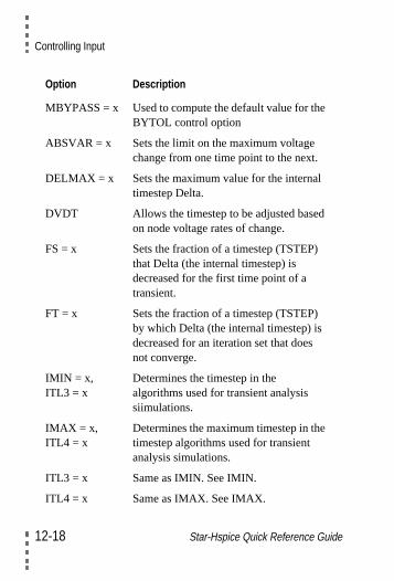
Controlling Input
MBYPASS = x Used to compute the default value for theBYTOL control option
ABSVAR = x Sets the limit on the maximum voltagechange from one time point to the next.
DELMAX = x Sets the maximum value for the internaltimestep Delta.
DVDT Allows the timestep to be adjusted basedon node voltage rates of change.
FS = x Sets the fraction of a timestep (TSTEP)that Delta (the internal timestep) isdecreased for the first time point of atransient.
FT = x Sets the fraction of a timestep (TSTEP)by which Delta (the internal timestep) isdecreased for an iteration set that doesnot converge.
IMIN = x,ITL3 = x
Determines the timestep in thealgorithms used for transient analysissiimulations.
IMAX = x,ITL4 = x
Determines the maximum timestep in thetimestep algorithms used for transientanalysis simulations.
ITL3 = x Same as IMIN. See IMIN.
ITL4 = x Same as IMAX. See IMAX.
Option Description
12-18 Star-Hspice Quick Reference Guide
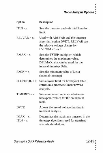
Model Analysis Options
ITL5 = x Sets the transient analysis total iterationlimit.
RELVAR = x Used with ABSVAR and the timestepalgorithm option DVDT. RELVAR setsthe relative voltage change forLVLTIM = 1 or 3.
RMAX = x Sets the TSTEP multiplier, whichdetermines the maximum value,DELMAX, that can be used for theinternal timestep Delta.
RMIN = x Sets the minimum value of Delta(internal timestep)
SLOPETOL = x Sets a lower limit for breakpoint tableentries in a piecewise linear (PWL)analysis.
TIMERES = x Sets a minimum separation betweenbreakpoint values for the breakpointtable.
DVTR Allows the use of voltage limiting intransient analysis.
IMAX = x,ITL4 = x
Determines the maximum timestep in thetimestep algorithms used for transientanalysis simulations.
Option Description
Star-Hspice Quick Reference Guide 12-19
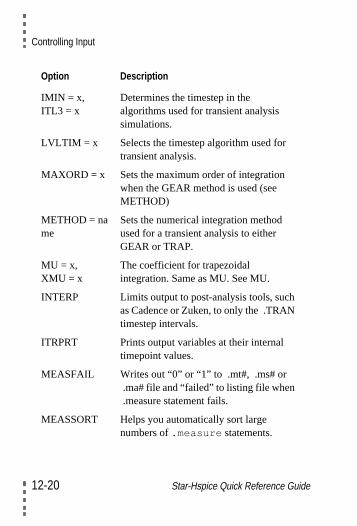
Controlling Input
IMIN = x,ITL3 = x
Determines the timestep in thealgorithms used for transient analysissimulations.
LVLTIM = x Selects the timestep algorithm used fortransient analysis.
MAXORD = x Sets the maximum order of integrationwhen the GEAR method is used (seeMETHOD)
METHOD = name
Sets the numerical integration methodused for a transient analysis to eitherGEAR or TRAP.
MU = x,XMU = x
The coefficient for trapezoidalintegration. Same as MU. See MU.
INTERP Limits output to post-analysis tools, suchas Cadence or Zuken, to only the .TRANtimestep intervals.
ITRPRT Prints output variables at their internaltimepoint values.
MEASFAIL Writes out “0” or “1” to .mt#, .ms# or.ma# file and “failed” to listing file when.measure statement fails.
MEASSORT Helps you automatically sort largenumbers of.measure statements.
Option Description
12-20 Star-Hspice Quick Reference Guide
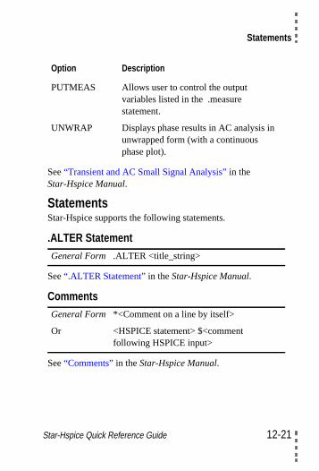
Statements
See“Transient and AC Small Signal Analysis” in theStar-Hspice Manual.
StatementsStar-Hspice supports the following statements.
.ALTER Statement
See“.ALTER Statement” in theStar-Hspice Manual.
Comments
See“Comments” in theStar-Hspice Manual.
PUTMEAS Allows user to control the outputvariables listed in the .measurestatement.
UNWRAP Displays phase results in AC analysis inunwrapped form (with a continuousphase plot).
General Form .ALTER <title_string>
General Form *<Comment on a line by itself>
Or <HSPICE statement> $<commentfollowing HSPICE input>
Option Description
Star-Hspice Quick Reference Guide 12-21
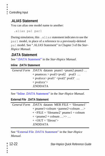
Controlling Input
.ALIAS StatementYou can alias one model name to another:
.alias pa1 par1
During simulation, this.alias statement indicates to use thepar1 model, in place of a reference to a previously-deletedpa1 model. See “.ALIAS Statement” in Chapter 3 of theStar-Hspice Manual.
.DATA StatementSee“.DATA Statement” in theStar-Hspice Manual.
Inline .DATA Statement
See“Inline .DATA Statement” in theStar-Hspice Manual.
External File .DATA Statement
See“External File .DATA Statement” in theStar-HspiceManual.
General Form .DATA datanm pnam1 <pnam2 pnam3 …+ pnamxxx > pval1<pval2 pval3 …+ pvalxxx> pval1’ <pval2’ pval3’ …+ pvalxxx’>.ENDDATA
General Form .DATA datanm MER FILE = ‘filename1’+ pname1=colnum <panme2=colnum …>+ <FILE = ‘filename2’ pname1 = colnum+ <pname2 = colnum …>> …+ <OUT = ‘fileout’>.ENDDATA
12-22 Star-Hspice Quick Reference Guide
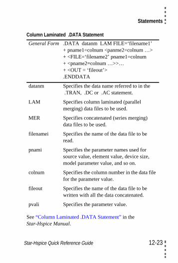
Statements
Column Laminated .DATA Statement
See“Column Laminated .DATA Statement” in theStar-Hspice Manual.
General Form .DATA datanm LAM FILE=‘filename1’+ pname1=colnum <panme2=colnum …>+ <FILE=‘filename2’ pname1=colnum+ <pname2=colnum …>>…+ <OUT = ‘fileout’>.ENDDATA
datanm Specifies the data name referred to in the.TRAN, .DC or .AC statement.
LAM Specifies column laminated (parallelmerging) data files to be used.
MER Specifies concatenated (series merging)data files to be used.
filenamei Specifies the name of the data file to beread.
pnami Specifies the parameter names used forsource value, element value, device size,model parameter value, and so on.
colnum Specifies the column number in the data filefor the parameter value.
fileout Specifies the name of the data file to bewritten with all the data concatenated.
pvali Specifies the parameter value.
Star-Hspice Quick Reference Guide 12-23
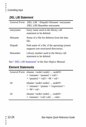
Controlling Input
.DEL LIB Statement
See“.DEL LIB Statement” in theStar-Hspice Manual.
Element Statements
General Form .DEL LIB ‘<filepath>filename’ entryname.DEL LIB libnumber entryname
entryname Entry name used in the library callstatement to be deleted.
filename Name of a file for deletion from the datafile.
filepath Path name of a file, if the operating systemsupports tree-structured directories.
libnumber Library number used in the library callstatement to be deleted.
General Form elname<node1 node2 … nodeN>+ <mname> <pname1 = val1>+ <pname2 = val2> <M = val>
Or elname <node1 node2 … nodeN>+ <mname> <pname = ‘expression’>+ <M = val>
Or elname <node1 node2 … nodeN>+ <mname> <val1 val2 … valn>
12-24 Star-Hspice Quick Reference Guide
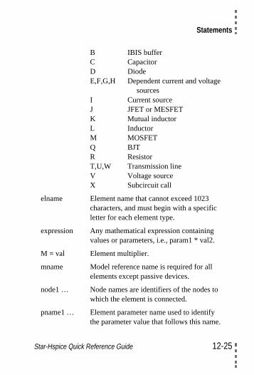
Statements
B IBIS bufferC CapacitorD DiodeE,F,G,H Dependent current and voltage
sourcesI Current sourceJ JFET or MESFETK Mutual inductorL InductorM MOSFETQ BJTR ResistorT,U,W Transmission lineV Voltage sourceX Subcircuit call
elname Element name that cannot exceed 1023characters, and must begin with a specificletter for each element type.
expression Any mathematical expression containingvalues or parameters, i.e., param1 * val2.
M = val Element multiplier.
mname Model reference name is required for allelements except passive devices.
node1 … Node names are identifiers of the nodes towhich the element is connected.
pname1 … Element parameter name used to identifythe parameter value that follows this name.
Star-Hspice Quick Reference Guide 12-25
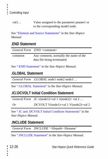
Controlling Input
r
See“Element and Source Statements” in theStar-HspiceManual.
.END Statement
See“.END Statement” in theStar-Hspice Manual.
.GLOBAL Statement
See“.GLOBAL Statement” in theStar-Hspice Manual.
.IC/.DCVOLT Initial Condition Statement
See“.IC and .DCVOLT Initial Condition Statements” in theStar-Hspice Manual.
.INCLUDE Statement
See“.INCLUDE Statement” in theStar-Hspice Manual.
val1… Value assigned to the parameter pname1 oto the corresponding model node.
General Form .END <comment>
comment Any comment, normally the name of thedata file being terminated.
General Form .GLOBAL node1 node2 node3 …
General Form .IC v(node1)=val 1 v(node2)= val 2 …
Or .DCVOLT V(node1)=val 1 V(node2)=val 2
General Form .INCLUDE ‘<filepath> filename’
12-26 Star-Hspice Quick Reference Guide
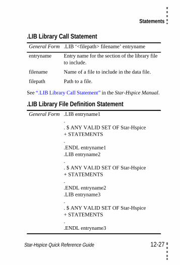
Statements
.LIB Library Call Statement
See“.LIB Library Call Statement”in theStar-Hspice Manual.
.LIB Library File Definition Statement
General Form .LIB ‘<filepath> filename’ entryname
entryname Entry name for the section of the library fileto include.
filename Name of a file to include in the data file.
filepath Path to a file.
General Form .LIB entryname1.. $ ANY VALID SET OF Star-Hspice+ STATEMENTS..ENDL entryname1.LIB entryname2.. $ ANY VALID SET OF Star-Hspice+ STATEMENTS..ENDL entryname2.LIB entryname3.. $ ANY VALID SET OF Star-Hspice+ STATEMENTS..ENDL entryname3
Star-Hspice Quick Reference Guide 12-27
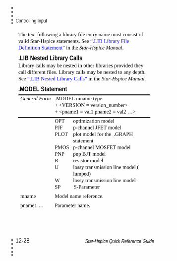
Controlling Input
.
The text following a library file entry name must consist ofvalid Star-Hspice statements. See“.LIB Library FileDefinition Statement” in theStar-Hspice Manual.
.LIB Nested Library CallsLibrary calls may be nested in other libraries provided theycall different files. Library calls may be nested to any depthSee“.LIB Nested Library Calls” in theStar-Hspice Manual.
.MODEL StatementGeneral Form .MODEL mname type
+ <VERSION = version_number>+ <pname1 = val1 pname2 = val2 …>
OPT optimization modelPJF p-channel JFET modelPLOT plot model for the .GRAPH
statementPMOS p-channel MOSFET modelPNP pnp BJT modelR resistor modelU lossy transmission line model (
lumped)W lossy transmission line modelSP S-Parameter
mname Model name reference.
pname1 … Parameter name.
12-28 Star-Hspice Quick Reference Guide
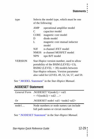
Statements
See“.MODEL Statement” in theStar-Hspice Manual.
.NODESET Statement
See“.NODESET Statement” in theStar-Hspice Manual.
type Selects the model type, which must be oneof the following:
AMP operational amplifier modelC capacitor modelCORE magnetic core modelD diode modelL magnetic core mutual inductor
modelNJF n-channel JFET modelNMOS n-channel MOSFET modelNPN npn BJT model
VERSION Star-Hspice version number, used to allowportability of the BSIM (LEVEL=13),BSIM2 (LEVEL = 39) models betweenStar-Hspice releases. Version parameteralso valid for LEVEL 49, 53, 54, 57, and 59.
General Form .NODESET V(node1) = val1+ <V(node2) = val2 …>
Or .NODESET node1 val1 <node2 val2>
node1… Node numbers or node names can includefull path names or circuit numbers
Star-Hspice Quick Reference Guide 12-29
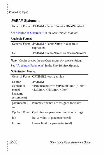
Controlling Input
.PARAM Statement
See“.PARAM Statement” in theStar-Hspice Manual.
Algebraic Format
Note: Quotes around the algebraic expression are mandatory.
See“Algebraic Parameter” in theStar-Hspice Manual.
Optimization Format
General Form .PARAM <ParamName>=<RealNumber>
General Form .PARAM <ParamName>=‘algebraicexpression’
Or .PARAM<ParamName1>=<ParamName2>
General Form OPTIMIZE=opt_pav_fun
Or (forelement ormodelkeynameassignment)
.PARAM<ParamName>=<OptParamFunc> (<Init>,<LoLim>, <Hi Lim>, <Inc>)
paramname1…
Parameter names are assigned to values
OptParmFunc Optimization parameter function (string)
Init Initial value of parameter (real)
LoLim Lower limit for parameter (real)
12-30 Star-Hspice Quick Reference Guide
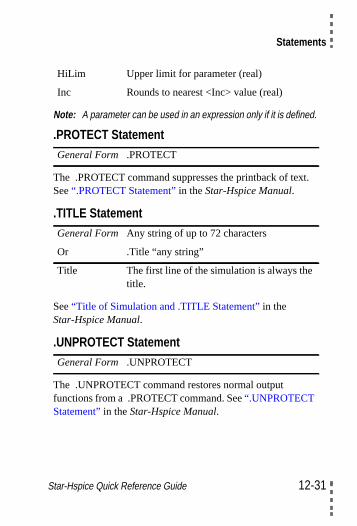
Statements
t.
Note: A parameter can be used in an expression only if it is defined.
.PROTECT Statement
The .PROTECT command suppresses the printback of texSee“.PROTECT Statement” in theStar-Hspice Manual.
.TITLE Statement
See“Title of Simulation and .TITLE Statement” in theStar-Hspice Manual.
.UNPROTECT Statement
The .UNPROTECT command restores normal outputfunctions from a .PROTECT command. See“.UNPROTECTStatement” in theStar-Hspice Manual.
HiLim Upper limit for parameter (real)
Inc Rounds to nearest <Inc> value (real)
General Form .PROTECT
General Form Any string of up to 72 characters
Or .Title “any string”
Title The first line of the simulation is always thetitle.
General Form .UNPROTECT
Star-Hspice Quick Reference Guide 12-31
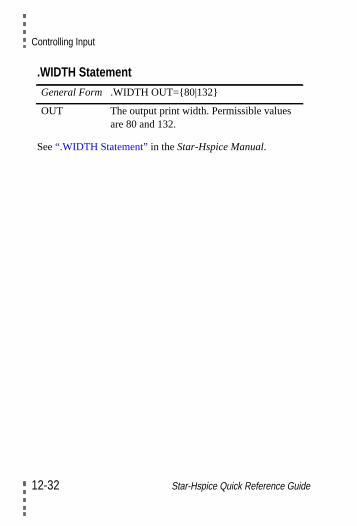
Controlling Input
.WIDTH Statement
See“.WIDTH Statement” in theStar-Hspice Manual.
General Form .WIDTH OUT={80|132}
OUT The output print width. Permissible valuesare 80 and 132.
12-32 Star-Hspice Quick Reference Guide
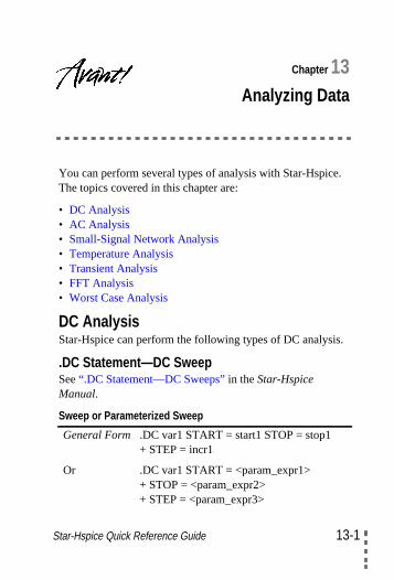
Star-Hspice Quic
13-
Chapter 13Analyzing Data
.
.
You can perform several types of analysis with Star-HspiceThe topics covered in this chapter are:
• DC Analysis• AC Analysis• Small-Signal Network Analysis• Temperature Analysis• Transient Analysis• FFT Analysis• Worst Case Analysis
DC AnalysisStar-Hspice can perform the following types of DC analysis
.DC Statement—DC SweepSee“.DC Statement—DC Sweeps” in theStar-HspiceManual.
Sweep or Parameterized Sweep
General Form .DC var1 START = start1 STOP = stop1+ STEP = incr1
Or .DC var1 START = <param_expr1>+ STOP = <param_expr2>+ STEP = <param_expr3>
k Reference Guide 13-1
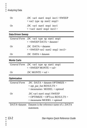
Analyzing Data
Data-Driven Sweep
Monte Carlo
Optimization
Or .DC var1 start1 stop1 incr1 <SWEEP+ var2 type np start2 stop2>
Or .DC var1 start1 stop1 incr1+ <var2 start2 stop2 incr2 >
General Form .DC var1 type np start1 stop1+ <SWEEP DATA = datanm>
Or .DC DATA = datanm+ <SWEEP var2 start2 stop2 incr2>
Or .DC DATA = datanm
General Form .DC var1 type np start1 stop1+ <SWEEP MONTE = val>
Or .DC MONTE = val >
General Form .DC DATA = datanm OPTIMIZE =+ opt_par_fun RESULTS =+ measnames MODEL = optmod
Or .DC var1 start1 stop1 SWEEP+ OPTIMIZE = OPTxxx RESULTS =+ measname MODEL = optmod
DATA=datanm Datanm is the reference name of a .DATAstatement.
13-2 Star-Hspice Quick Reference Guide
DC Analysis
t
l
incr1 … Voltage, current, element, modelparameters, or temperature incrementvalues.
MODEL Optimization reference name used inthe .MODEL OPT statement.
MONTE=val Produces a numberval of randomlygenerated values, which are used to selecparameters from a distribution.
np Number of points per decade (ordepending on the preceding keyword).
OPTIMIZE Specifies the parameter reference nameused in the .PARAM statement.
RESULTS Specifies the measure name used inthe .MEASURE statement.
start1 … Starting voltage, current, element, modelparameters, or temperature values.
stop1 … Final voltage, current, any element, modeparameter, or temperature values.
SWEEP Indicates a second sweep has differenttype of variation (DEC, OCT, LIN, POI,DATA statement, or MONTE = val).
TEMP Indicates a temperature sweep.
type Can be any of the following keywords:DEC, OCT, LIN, POI.
Star-Hspice Quick Reference Guide 13-3
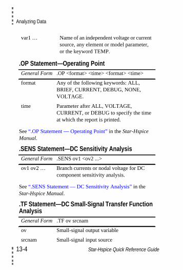
Analyzing Data
t
13-4 Star-Hspice Quick Reference Guide
.OP Statement—Operating Point
See“.OP Statement — Operating Point” in theStar-HspiceManual.
.SENS Statement—DC Sensitivity Analysis
See“.SENS Statement — DC Sensitivity Analysis” in theStar-Hspice Manual.
.TF Statement—DC Small-Signal Transfer FunctionAnalysis
var1 … Name of an independent voltage or currensource, any element or model parameter,or the keyword TEMP.
General Form .OP <format> <time> <format> <time>
format Any of the following keywords: ALL,BRIEF, CURRENT, DEBUG, NONE,VOLTAGE.
time Parameter after ALL, VOLTAGE,CURRENT, or DEBUG to specify the timeat which the report is printed.
General Form .SENS ov1 <ov2 ...>
ov1 ov2 … Branch currents or nodal voltage for DCcomponent sensitivity analysis.
General Form .TF ov srcnam
ov Small-signal output variable
srcnam Small-signal input source
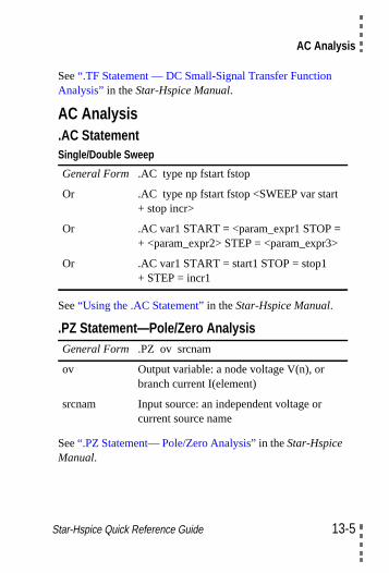
AC Analysis
See“.TF Statement — DC Small-Signal Transfer FunctionAnalysis” in theStar-Hspice Manual.
AC Analysis.AC StatementSingle/Double Sweep
See“Using the .AC Statement” in theStar-Hspice Manual.
.PZ Statement—Pole/Zero Analysis
See“.PZ Statement— Pole/Zero Analysis”in theStar-HspiceManual.
General Form .AC type np fstart fstop
Or .AC type np fstart fstop <SWEEP var start+ stop incr>
Or .AC var1 START = <param_expr1 STOP =+ <param_expr2> STEP = <param_expr3>
Or .AC var1 START = start1 STOP = stop1+ STEP = incr1
General Form .PZ ov srcnam
ov Output variable: a node voltage V(n), orbranch current I(element)
srcnam Input source: an independent voltage orcurrent source name
Star-Hspice Quick Reference Guide 13-5
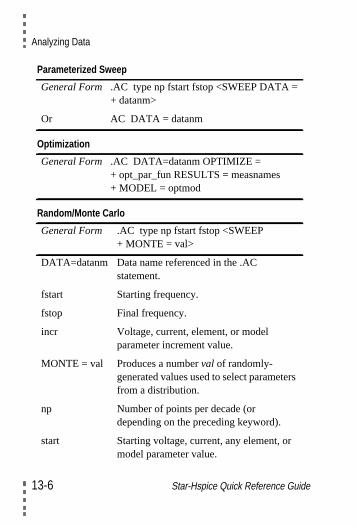
Analyzing Data
s
Parameterized Sweep
Optimization
Random/Monte Carlo
General Form .AC type np fstart fstop <SWEEP DATA =+ datanm>
Or AC DATA = datanm
General Form .AC DATA=datanm OPTIMIZE =+ opt_par_fun RESULTS = measnames+ MODEL = optmod
General Form .AC type np fstart fstop <SWEEP+ MONTE = val>
DATA=datanm Data name referenced in the .ACstatement.
fstart Starting frequency.
fstop Final frequency.
incr Voltage, current, element, or modelparameter increment value.
MONTE = val Produces a numberval of randomly-generated values used to select parameterfrom a distribution.
np Number of points per decade (ordepending on the preceding keyword).
start Starting voltage, current, any element, ormodel parameter value.
13-6 Star-Hspice Quick Reference Guide
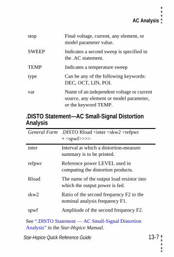
AC Analysis
.DISTO Statement—AC Small-Signal DistortionAnalysis
See“.DISTO Statement — AC Small-Signal DistortionAnalysis” in theStar-Hspice Manual.
stop Final voltage, current, any element, ormodel parameter value.
SWEEP Indicates a second sweep is specified inthe .AC statement.
TEMP Indicates a temperature sweep
type Can be any of the following keywords:DEC, OCT, LIN, POI.
var Name of an independent voltage or currentsource, any element or model parameter,or the keyword TEMP.
General Form .DISTO Rload <inter <skw2 <refpwr+ <spwf>>>>
inter Interval at which a distortion-measuresummary is to be printed.
refpwr Reference power LEVEL used incomputing the distortion products.
Rload The name of the output load resistor intowhich the output power is fed.
skw2 Ratio of the second frequency F2 to thenominal analysis frequency F1.
spwf Amplitude of the second frequency F2.
Star-Hspice Quick Reference Guide 13-7
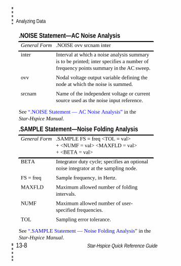
Analyzing Data
t
13-8 Star-Hspice Quick Reference Guide
.NOISE Statement—AC Noise Analysis
See“.NOISE Statement — AC Noise Analysis” in theStar-Hspice Manual.
.SAMPLE Statement—Noise Folding Analysis
See“.SAMPLE Statement — Noise Folding Analysis” in theStar-Hspice Manual.
General Form .NOISE ovv srcnam inter
inter Interval at which a noise analysis summaryis to be printed; inter specifies a number offrequency points summary in the AC sweep.
ovv Nodal voltage output variable defining thenode at which the noise is summed.
srcnam Name of the independent voltage or currensource used as the noise input reference.
General Form .SAMPLE FS = freq <TOL = val>+ <NUMF = val> <MAXFLD = val>+ <BETA = val>
BETA Integrator duty cycle; specifies an optionalnoise integrator at the sampling node.
FS = freq Sample frequency, in Hertz.
MAXFLD Maximum allowed number of foldingintervals.
NUMF Maximum allowed number of user-specified frequencies.
TOL Sampling error tolerance.
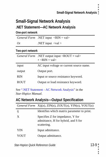
Small-Signal Network Analysis
Small-Signal Network Analysis.NET Statement—AC Network AnalysisOne-port network
Two-port network
See“.NET Statement - AC Network Analysis” in theStar-Hspice Manual.
AC Network Analysis—Output Specification
General Form .NET input <RIN = val>
Or .NET input <val >
General Form .NET output input <ROUT = val>+ <RIN = val>
input AC input voltage or current source name.
output Output port.
RIN Input or source resistance keyword.
ROUT Output or load resistance keyword.
General Form Xij(z), ZIN(z), ZOUT(z), YIN(z), YOUT(z)
ij Identifies which matrix parameter to print.
X Specifies Z for impedance, Y foradmittance, H for hybrid, and S forscattering.
YIN Input admittance.
YOUT Output admittance.
Star-Hspice Quick Reference Guide 13-9
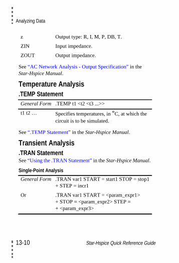
Analyzing Data
See“AC Network Analysis - Output Specification” in theStar-Hspice Manual.
Temperature Analysis.TEMP Statement
See“.TEMP Statement” in theStar-Hspice Manual.
Transient Analysis.TRAN StatementSee“Using the .TRAN Statement”in theStar-Hspice Manual.
Single-Point Analysis
z Output type: R, I, M, P, DB, T.
ZIN Input impedance.
ZOUT Output impedance.
General Form .TEMP t1 <t2 <t3 ...>>
t1 t2 … Specifies temperatures, in°C, at which thecircuit is to be simulated.
General Form .TRAN var1 START = start1 STOP = stop1+ STEP = incr1
Or .TRAN var1 START = <param_expr1>+ STOP = <param_expr2> STEP =+ <param_expr3>
13-10 Star-Hspice Quick Reference Guide
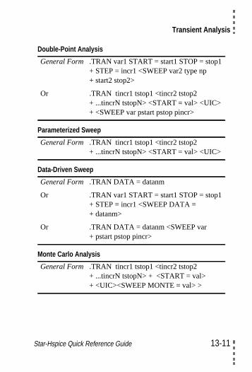
Transient Analysis
Double-Point Analysis
Parameterized Sweep
Data-Driven Sweep
Monte Carlo Analysis
General Form .TRAN var1 START = start1 STOP = stop1+ STEP = incr1 <SWEEP var2 type np+ start2 stop2>
Or .TRAN tincr1 tstop1 <tincr2 tstop2+ ...tincrN tstopN> <START = val> <UIC>+ <SWEEP var pstart pstop pincr>
General Form .TRAN tincr1 tstop1 <tincr2 tstop2+ ...tincrN tstopN> <START = val> <UIC>
General Form .TRAN DATA = datanm
Or .TRAN var1 START = start1 STOP = stop1+ STEP = incr1 <SWEEP DATA =+ datanm>
Or .TRAN DATA = datanm <SWEEP var+ pstart pstop pincr>
General Form .TRAN tincr1 tstop1 <tincr2 tstop2+ ...tincrN tstopN> + <START = val>+ <UIC><SWEEP MONTE = val> >
Star-Hspice Quick Reference Guide 13-11
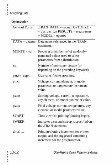
Analyzing Data
Optimization
General Form .TRAN DATA = datanm OPTIMIZE =+ opt_par_fun RESULTS = measnames+ MODEL = optmod
DATA = datanm Data name referenced in the .TRANstatement.
MONTE = val Produces a numberval of randomly-generated values used to selectparameters from a distribution.
np Number of points per decade (ordepending on the preceding keyword).
param_expr... User-specified expressions.
pincr Voltage, current, element, or modelparameter, or temperature incrementvalue.
pstart Starting voltage, current, temperature,any element, or model parameter value.
pstop Final voltage, current, temperature, anyelement, or model parameter value.
START Time at which printing/plotting begins.
SWEEP Indicates a second sweep is specified onthe .TRAN statement.
tincr1… Printing/plotting increment for printeroutput, and the suggested computingincrement for the postprocessor.
13-12 Star-Hspice Quick Reference Guide
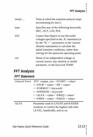
FFT Analysis
FFT Analysis.FFT Statement
tstop1… Time at which the transient analysis stopsincrementing by tincr1.
type Specifies any of the following keywords:DEC, OCT, LIN, POI.
UIC Causes Star-Hspice to use the nodalvoltages specified in the .IC statement (orby the “IC = ” parameters in the variouselement statements) to calculate theinitial transient conditions, rather thansolving for the quiescent operating point.
var Name of an independent voltage orcurrent source, any element or modelparameter, or the keyword TEMP.
General Form .FFT <output_var> <START = value>+ <STOP = value> <NP = value>+ <FORMAT = keyword>+ <WINDOW = keyword>+ <ALFA = value> <FREQ = value>+ <FMIN = value> <FMAX = value>
ALFA Parameter used in GAUSS and KAISERwindows to control the highest side-lobeLEVEL, bandwidth, and so on.
Star-Hspice Quick Reference Guide 13-13
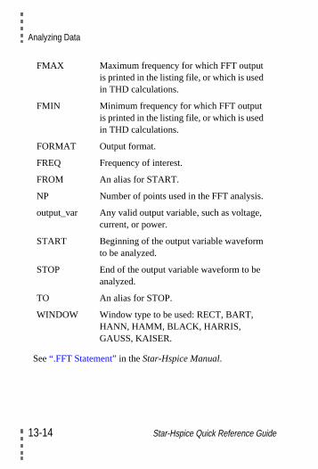
Analyzing Data
See“.FFT Statement” in theStar-Hspice Manual.
FMAX Maximum frequency for which FFT outputis printed in the listing file, or which is usedin THD calculations.
FMIN Minimum frequency for which FFT outputis printed in the listing file, or which is usedin THD calculations.
FORMAT Output format.
FREQ Frequency of interest.
FROM An alias for START.
NP Number of points used in the FFT analysis.
output_var Any valid output variable, such as voltage,current, or power.
START Beginning of the output variable waveformto be analyzed.
STOP End of the output variable waveform to beanalyzed.
TO An alias for STOP.
WINDOW Window type to be used: RECT, BART,HANN, HAMM, BLACK, HARRIS,GAUSS, KAISER.
13-14 Star-Hspice Quick Reference Guide
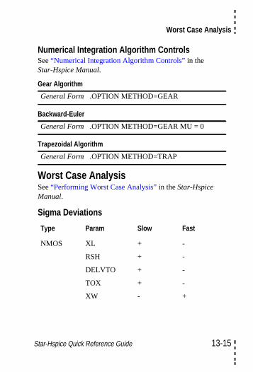
Worst Case Analysis
Numerical Integration Algorithm ControlsSee“Numerical Integration Algorithm Controls” in theStar-Hspice Manual.
Gear Algorithm
Backward-Euler
Trapezoidal Algorithm
Worst Case AnalysisSee“Performing Worst Case Analysis” in theStar-HspiceManual.
Sigma Deviations
General Form .OPTION METHOD=GEAR
General Form .OPTION METHOD=GEAR MU = 0
General Form .OPTION METHOD=TRAP
Type Param Slow Fast
NMOS XL + -
RSH + -
DELVTO + -
TOX + -
XW - +
Star-Hspice Quick Reference Guide 13-15
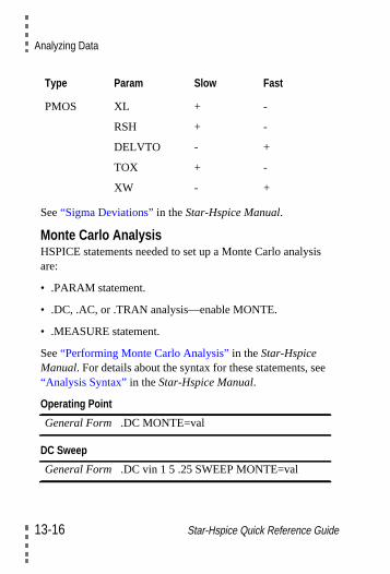
Analyzing Data
is
ee
See“Sigma Deviations” in theStar-Hspice Manual.
Monte Carlo AnalysisHSPICE statements needed to set up a Monte Carlo analysare:
• .PARAM statement.
• .DC, .AC, or .TRAN analysis—enable MONTE.
• .MEASURE statement.
See“Performing Monte Carlo Analysis” in theStar-HspiceManual. For details about the syntax for these statements, s“Analysis Syntax” in theStar-Hspice Manual.
Operating Point
DC Sweep
PMOS XL + -
RSH + -
DELVTO - +
TOX + -
XW - +
General Form .DC MONTE=val
General Form .DC vin 1 5 .25 SWEEP MONTE=val
Type Param Slow Fast
13-16 Star-Hspice Quick Reference Guide
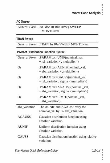
Worst Case Analysis
AC Sweep
TRAN Sweep
.PARAM Distribution Function Syntax
General Form .AC dec 10 100 10meg SWEEP+ MONTE=val
General Form .TRAN 1n 10n SWEEP MONTE=val
General Form .PARAM xx=UNIF(nominal_val,+ rel_variation <, multiplier>)
Or .PARAM xx=AUNIF(nominal_val,+ abs_variation <,multiplier>)
Or .PARAM xx=GAUSS(nominal_val,+ rel_variation, sigma <,multiplier>)
Or .PARAM xx=AGAUSS(nominal_val,+ abs_variation, sigma <,multiplier>)
Or .PARAM xx=LIMIT(nominal_val,+ abs_variation)
abs_variation The AUNIF and AGAUSS vary thenominal_val by +/- abs_variation.
AGAUSS Gaussian distribution function usingabsolute variation.
AUNIF Uniform distribution function usingabsolute variation.
GAUSS Gaussian distribution function using relativevariation.
Star-Hspice Quick Reference Guide 13-17
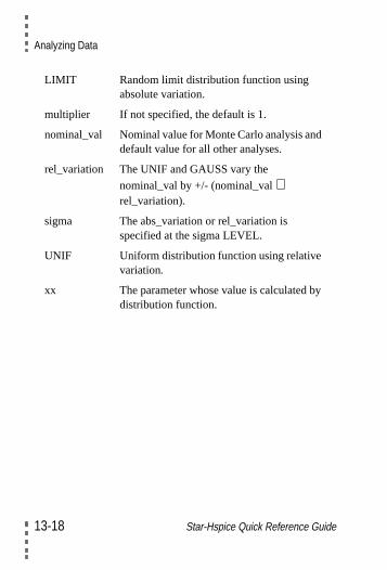
Analyzing Data
LIMIT Random limit distribution function usingabsolute variation.
multiplier If not specified, the default is 1.
nominal_val Nominal value for Monte Carlo analysis anddefault value for all other analyses.
rel_variation The UNIF and GAUSS vary the
nominal_val by +/- (nominal_val⋅rel_variation).
sigma The abs_variation or rel_variation isspecified at the sigma LEVEL.
UNIF Uniform distribution function using relativevariation.
xx The parameter whose value is calculated bydistribution function.
13-18 Star-Hspice Quick Reference Guide
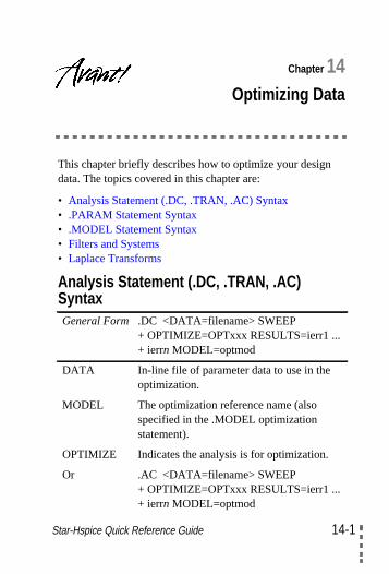
Star-Hspice Quic
14-
Chapter 14Optimizing Data
This chapter briefly describes how to optimize your designdata. The topics covered in this chapter are:
• Analysis Statement (.DC, .TRAN, .AC) Syntax• .PARAM Statement Syntax• .MODEL Statement Syntax• Filters and Systems• Laplace Transforms
Analysis Statement (.DC, .TRAN, .AC)SyntaxGeneral Form .DC <DATA=filename> SWEEP
+ OPTIMIZE=OPTxxx RESULTS=ierr1 ...+ ierrn MODEL=optmod
DATA In-line file of parameter data to use in theoptimization.
MODEL The optimization reference name (alsospecified in the .MODEL optimizationstatement).
OPTIMIZE Indicates the analysis is for optimization.
Or .AC <DATA=filename> SWEEP+ OPTIMIZE=OPTxxx RESULTS=ierr1 ...+ ierrn MODEL=optmod
k Reference Guide 14-1
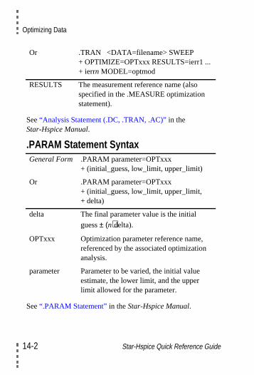
Optimizing Data
See“Analysis Statement (.DC, .TRAN, .AC)” in theStar-Hspice Manual.
.PARAM Statement Syntax
See“.PARAM Statement” in theStar-Hspice Manual.
Or .TRAN <DATA=filename> SWEEP+ OPTIMIZE=OPTxxx RESULTS=ierr1 ...+ ierrn MODEL=optmod
RESULTS The measurement reference name (alsospecified in the .MEASURE optimizationstatement).
General Form .PARAM parameter=OPTxxx+ (initial_guess, low_limit, upper_limit)
Or .PARAM parameter=OPTxxx+ (initial_guess, low_limit, upper_limit,+ delta)
delta The final parameter value is the initial
guess± (n⋅delta).
OPTxxx Optimization parameter reference name,referenced by the associated optimizationanalysis.
parameter Parameter to be varied, the initial valueestimate, the lower limit, and the upperlimit allowed for the parameter.
14-2 Star-Hspice Quick Reference Guide
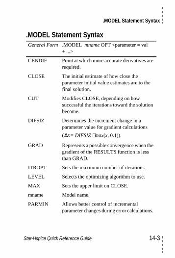
.MODEL Statement Syntax
e
.
.MODEL Statement SyntaxGeneral Form .MODEL mname OPT <parameter = val
+ ...>
CENDIF Point at which more accurate derivatives arerequired.
CLOSE The initial estimate of how close theparameter initial value estimates are to thefinal solution.
CUT Modifies CLOSE, depending on howsuccessful the iterations toward the solutionbecome.
DIFSIZ Determines the increment change in aparameter value for gradient calculations
( = DIFSIZ ⋅ max(x, 0.1)).
GRAD Represents a possible convergence when thgradient of the RESULTS function is lessthan GRAD.
ITROPT Sets the maximum number of iterations.
LEVEL Selects the optimizing algorithm to use.
MAX Sets the upper limit on CLOSE.
mname Model name.
PARMIN Allows better control of incrementalparameter changes during error calculations
∆x
Star-Hspice Quick Reference Guide 14-3
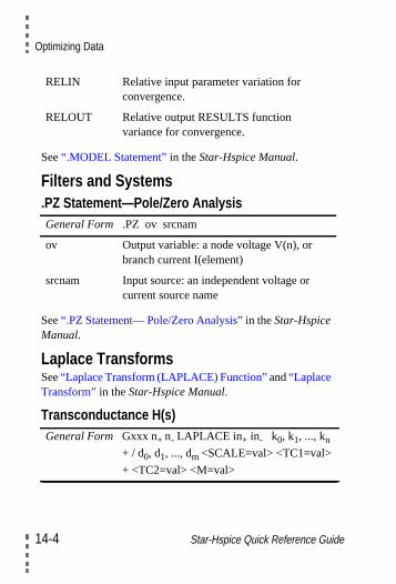
Optimizing Data
See“.MODEL Statement” in theStar-Hspice Manual.
Filters and Systems.PZ Statement—Pole/Zero Analysis
See“.PZ Statement— Pole/Zero Analysis”in theStar-HspiceManual.
Laplace TransformsSee“Laplace Transform (LAPLACE) Function”and“LaplaceTransform” in theStar-Hspice Manual.
Transconductance H(s)
RELIN Relative input parameter variation forconvergence.
RELOUT Relative output RESULTS functionvariance for convergence.
General Form .PZ ov srcnam
ov Output variable: a node voltage V(n), orbranch current I(element)
srcnam Input source: an independent voltage orcurrent source name
General Form Gxxx n+ n- LAPLACE in+ in- k0, k1, ..., kn+ / d0, d1, ..., dm <SCALE=val> <TC1=val>
+ <TC2=val> <M=val>
14-4 Star-Hspice Quick Reference Guide
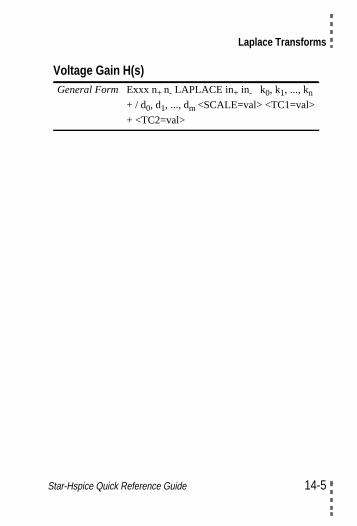
Laplace Transforms
Voltage Gain H(s)General Form Exxx n+ n- LAPLACE in+ in- k0, k1, ..., kn
+ / d0, d1, ..., dm <SCALE=val> <TC1=val>
+ <TC2=val>
Star-Hspice Quick Reference Guide 14-5
Optimizing Data
14-6 Star-Hspice Quick Reference Guide
Star-Hspice Quic
15-
Chapter 15Output Format
,
t
The topics covered in this chapter are:
• Graphing Results in AvanWaves
• AC Analysis
• Print Commands
• DC and Transient Output
• Power Output
• AC Analysis Output
• Element Template Output
• Element Template Listings
For a detailed description of graphing with HSPLOT and GSIsee theStar-Hspice Manual, Chapter 4, “Graphing.”
Graphing Results in AvanWavesThe .option POST must be placed in the Hspice netlist inpufile.
• POST or POST=1 creates a binary file.
• POST=2 creates an ascii file, portable to all supportedmachines.
k Reference Guide 15-1
Output Format
e
)
Limiting the Size of the Graph Data FileThe option PROBE limits the number of curves stored to thosnodes specified in the Hspice inputfile’s .PRINT, .PLOT, .OPTION PROBE, and .GRAPHstatements. The option INTERP (for transient analysis onlylimits the number of points stored. The option INTERPpreinterpolates the output to the interval specified onthe .TRAN statement.
Automatic Hardcopy During HSPICE RunA .GRAPH statement will automatically produce a hardcopyplot. A .TITLE placed before each .GRAPH will set the graphtitle. Otherwise, the simulation title will be used. The optionPOST in conjunction with .GRAPH will create a graph datafile.
Starting AvanWaves—Command lineAvanWaves’ command line definition is:
awaves [[-d] <path><design-name> [-c
+ <config_name>] [-laf(windows|openlook|motif)]
-d The name of the design to be opened oninvoking AvanWaves
-c Specifies that a previously savedconfiguration for the current design is to beused upon the initialization of AvanWaves.
-laf [windows|openlook|motif]
Specifies the window manager style to beused. The default is Motif.
15-2 Star-Hspice Quick Reference Guide
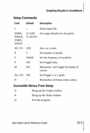
Graphing Results in AvanWaves
Setup Commands
Accessible Menus From Setup
Cmd Default Description
I -- Name input file.
XMIN,XMAX,YMIN,YMAX
X=LIMY=AUTO
Set range defaults for all panels.
XS, YS LIN Set x or y scale.
P 1 Set number of panels.
F NONE Set the frequency of symbols.
T ON Set/Toggle ticks.
M NO Monotonic. Set/Toggle for family ofcurves.
XG, YG ON Set/Toggle x or y grids.
D -- Reinitialize all Setup menu values.
G Bring up the Graph window.
N Bring up the Node window.
Q Exit the program.
Star-Hspice Quick Reference Guide 15-3
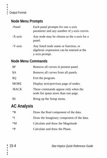
Output Format
.
Node Menu Prompts
Node Menu Commands
AC Analysis
-Panel Each panel prompts for one x-axisparameter and any number of y-axis curves
-X-axis Any node may be chosen as the x-axis for apanel.
-Y-axis Any listed node name or function, oralgebraic expression can be entered at they-axis prompt.
$P Remove all curves in present panel.
$A Remove all curves from all panels.
$Q Exit the program.
MORE Display next/previous page of nodes.
/BACK These commands appear only when thenode list spans more than one page.
$S Bring up the Setup menu.
*R Draw the Real component of the data.
*I Draw the Imaginary component of the data.
*M Calculate and draw the Magnitude
*P Calculate and draw the Phase.
15-4 Star-Hspice Quick Reference Guide
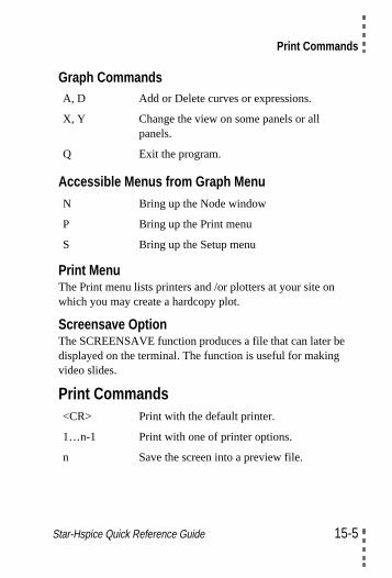
Print Commands
e
Graph Commands
Accessible Menus from Graph Menu
Print MenuThe Print menu lists printers and /or plotters at your site onwhich you may create a hardcopy plot.
Screensave OptionThe SCREENSAVE function produces a file that can later bdisplayed on the terminal. The function is useful for makingvideo slides.
Print Commands
A, D Add or Delete curves or expressions.
X, Y Change the view on some panels or allpanels.
Q Exit the program.
N Bring up the Node window
P Bring up the Print menu
S Bring up the Setup menu
<CR> Print with the default printer.
1…n-1 Print with one of printer options.
n Save the screen into a preview file.
Star-Hspice Quick Reference Guide 15-5
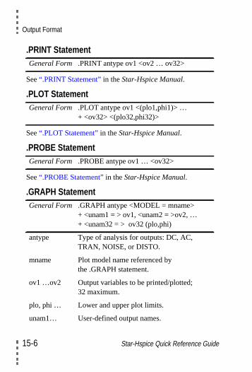
Output Format
.PRINT Statement
See“.PRINT Statement” in theStar-Hspice Manual.
.PLOT Statement
See“.PLOT Statement” in theStar-Hspice Manual.
.PROBE Statement
See“.PROBE Statement” in theStar-Hspice Manual.
.GRAPH Statement
General Form .PRINT antype ov1 <ov2 … ov32>
General Form .PLOT antype ov1 <(plo1,phi1)> …+ <ov32> <(plo32,phi32)>
General Form .PROBE antype ov1 … <ov32>
General Form .GRAPH antype <MODEL = mname>+ <unam1 = > ov1, <unam2 = >ov2, …+ <unam32 = > ov32 (plo,phi)
antype Type of analysis for outputs: DC, AC,TRAN, NOISE, or DISTO.
mname Plot model name referenced bythe .GRAPH statement.
ov1 …ov2 Output variables to be printed/plotted;32 maximum.
plo, phi … Lower and upper plot limits.
unam1… User-defined output names.
15-6 Star-Hspice Quick Reference Guide
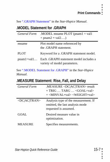
Print Commands
See“.GRAPH Statement” in theStar-Hspice Manual.
.MODEL Statement for .GRAPH
See“.MODEL Statement for .GRAPH” in theStar-HspiceManual.
.MEASURE Statement: Rise, Fall, and Delay
General Form .MODEL mname PLOT (pnam1 = val1+ pnam2 = val2….)
mname Plot model name referenced bythe .GRAPH statement.
PLOT Keyword for a .GRAPH statement model.
pnam1=val1… Each .GRAPH statement model includes avariety of model parameters.
General Form .MEASURE <DC|AC|TRAN> result+ TRIG … TARG … <GOAL=val>+ <MINVAL=val> <WEIGHT=val>
<DC|AC|TRAN> Analysis type of the measurement. Ifomitted, the last analysis moderequested is assumed.
GOAL Desired measure value inoptimization.
MEASURE Specifies measurements.
Star-Hspice Quick Reference Guide 15-7
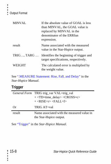
Output Format
n
See“.MEASURE Statement: Rise, Fall, and Delay” in theStar-Hspice Manual.
Trigger
See“Trigger” in theStar-Hspice Manual.
MINVAL If the absolute value of GOAL is lessthan MINVAL, the GOAL value isreplaced by MINVAL in thedenominator of the ERRfunexpression.
result Name associated with the measuredvalue in the Star-Hspice output.
TRIG…, TARG … Identifies the beginning of trigger andtarget specifications, respectively.
WEIGHT The calculated error is multiplied bythe weight value.
General Form TRIG trig_var VAL=trig_val+ <TD=time_delay> <CROSS=c>+ <RISE=r> <FALL=f>
Or TRIG AT=val
result Name associated with the measured value ithe Star-Hspice output.
15-8 Star-Hspice Quick Reference Guide

Print Commands
a
t
s
Target
See“Target” in theStar-Hspice Manual.
General Form TARG targ_var VAL = targ_val+ <TD = time_delay> <CROSS = c | LAST>+ <RISE = r | LAST> <FALL = f | LAST>
AT = val Special case for trigger specification.
CROSS = cRISE = rFALL = f
The numbers indicate which occurrence of CROSS, FALL, or RISE event causes ameasurement to be performed.
LAST Measurement is performed when the lastCROSS, FALL, or RISE event occurs.
TARG Beginning of the target signal specification.
targ_val Value of thetarg_var at which the counterfor crossing, rises, or falls is incremented byone.
targ_var Name of the output variable whosepropagation delay is determined with respecto thetrig_var.
time_delay Amount of simulation time that must elapsebefore the measurement is enabled.
TRIG Beginning of the trigger specification.
trig_val Value oftrig_var at which the counter forcrossing, rises, or falls increments by one.
trig_var Name of the output variable, that determinethe logical beginning of measurement.
Star-Hspice Quick Reference Guide 15-9
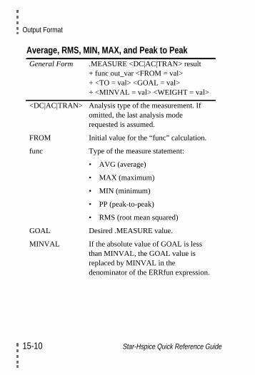
Output Format
Average, RMS, MIN, MAX, and Peak to PeakGeneral Form .MEASURE <DC|AC|TRAN> result
+ func out_var <FROM = val>+ <TO = val> <GOAL = val>+ <MINVAL = val> <WEIGHT = val>
<DC|AC|TRAN> Analysis type of the measurement. Ifomitted, the last analysis moderequested is assumed.
FROM Initial value for the “func” calculation.
func Type of the measure statement:
• AVG (average)
• MAX (maximum)
• MIN (minimum)
• PP (peak-to-peak)
• RMS (root mean squared)
GOAL Desired .MEASURE value.
MINVAL If the absolute value of GOAL is lessthan MINVAL, the GOAL value isreplaced by MINVAL in thedenominator of the ERRfun expression.
15-10 Star-Hspice Quick Reference Guide
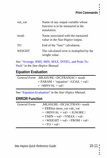
Print Commands
See“Average, RMS, MIN, MAX, INTEG, and Peak-To-Peak” in theStar-Hspice Manual.
Equation Evaluation
See“Equation Evaluation” in theStar-Hspice Manual.
ERROR Function
out_var Name of any output variable whosefunction is to be measured in thesimulation.
result Name associated with the measuredvalue in the Star-Hspice output.
TO End of the “func” calculation.
WEIGHT The calculated error is multiplied by theweight value.
General Form .MEASURE <DC|TRAN|AC> result+ PARAM = ‘equation’ <GOAL = val>+ <MINVAL = val>
General Form .MEASURE <DC|AC|TRAN> result+ ERRfun meas_var calc_var+ <MINVAL = val> < IGNORE |+ YMIN = val> <YMAX = val>+ <WEIGHT = val> <FROM = val>+ <TO = val>
Star-Hspice Quick Reference Guide 15-11
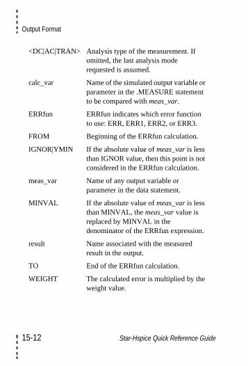
Output Format
<DC|AC|TRAN> Analysis type of the measurement. Ifomitted, the last analysis moderequested is assumed.
calc_var Name of the simulated output variable orparameter in the .MEASURE statementto be compared withmeas_var.
ERRfun ERRfun indicates which error functionto use: ERR, ERR1, ERR2, or ERR3.
FROM Beginning of the ERRfun calculation.
IGNOR|YMIN If the absolute value ofmeas_var is lessthan IGNOR value, then this point is notconsidered in the ERRfun calculation.
meas_var Name of any output variable orparameter in the data statement.
MINVAL If the absolute value ofmeas_var is lessthan MINVAL, themeas_var value isreplaced by MINVAL in thedenominator of the ERRfun expression.
result Name associated with the measuredresult in the output.
TO End of the ERRfun calculation.
WEIGHT The calculated error is multiplied by theweight value.
15-12 Star-Hspice Quick Reference Guide
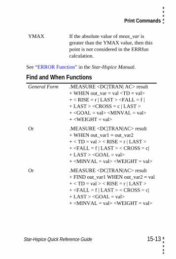
Print Commands
See“ERROR Function” in theStar-Hspice Manual.
Find and When Functions
YMAX If the absolute value ofmeas_var isgreater than the YMAX value, then thispoint is not considered in the ERRfuncalculation.
General Form .MEASURE <DC|TRAN| AC> result+ WHEN out_var = val <TD = val>+ < RISE = r | LAST > <FALL = f |+ LAST > <CROSS = c | LAST >+ <GOAL = val> <MINVAL = val>+ <WEIGHT = val>
Or .MEASURE <DC|TRAN|AC> result+ WHEN out_var1 = out_var2+ < TD = val > < RISE = r | LAST >+ <FALL = f | LAST > < CROSS = c|+ LAST > <GOAL = val>+ <MINVAL = val> <WEIGHT = val>
Or .MEASURE <DC|TRAN|AC> result+ FIND out_var1 WHEN out_var2 = val+ < TD = val > < RISE = r | LAST >+ <FALL = f | LAST > < CROSS = c|+ LAST > <GOAL = val>+ <MINVAL = val> <WEIGHT = val>
Star-Hspice Quick Reference Guide 15-13
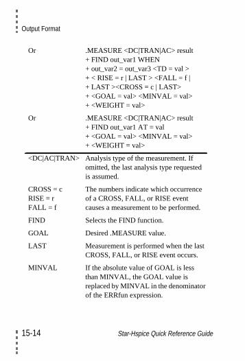
Output Format
.
t
Or .MEASURE <DC|TRAN|AC> result+ FIND out_var1 WHEN+ out_var2 = out_var3 <TD = val >+ < RISE = r | LAST > <FALL = f |+ LAST ><CROSS = c | LAST>+ <GOAL = val> <MINVAL = val>+ <WEIGHT = val>
Or .MEASURE <DC|TRAN|AC> result+ FIND out_var1 AT = val+ <GOAL = val> <MINVAL = val>+ <WEIGHT = val>
<DC|AC|TRAN> Analysis type of the measurement. Ifomitted, the last analysis type requestedis assumed.
CROSS = cRISE = rFALL = f
The numbers indicate which occurrenceof a CROSS, FALL, or RISE eventcauses a measurement to be performed
FIND Selects the FIND function.
GOAL Desired .MEASURE value.
LAST Measurement is performed when the lasCROSS, FALL, or RISE event occurs.
MINVAL If the absolute value of GOAL is lessthan MINVAL, the GOAL value isreplaced by MINVAL in the denominatorof the ERRfun expression.
15-14 Star-Hspice Quick Reference Guide
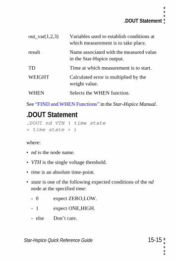
.DOUT Statement
t
e
See“FIND and WHEN Functions”in theStar-Hspice Manual.
.DOUT Statement
.DOUT nd VTH ( time state< time state > )
where:
• nd is the node name.
• VTH is the single voltage threshold.
• time is an absolute time-point.
• state is one of the following expected conditions of thendnode at the specifiedtime:
- 0 expect ZERO,LOW.
- 1 expect ONE,HIGH.
- else Don’t care.
out_var(1,2,3) Variables used to establish conditions awhich measurement is to take place.
result Name associated with the measured valuin the Star-Hspice output.
TD Time at which measurement is to start.
WEIGHT Calculated error is multiplied by theweight value.
WHEN Selects the WHEN function.
Star-Hspice Quick Reference Guide 15-15
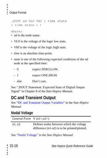
Output Format
.DOUT nd VLO VHI ( time state< time state > )
where:• nd is the node name.
• VLO is the voltage of the logic low state.
• VHI is the voltage of the logic high state.
• time is an absolute time-point.
• state is one of the following expected conditions of thendnode at the specifiedtime:
- 0 expect ZERO,LOW.
- 1 expect ONE,HIGH.
- else Don’t care.
See “.DOUT Statement: Expected State of Digital OutputSignal” in Chapter 8 of theStar-Hspice Manual.
DC and Transient OutputSee“DC and Transient Output Variables” in theStar-HspiceManual.
Nodal Voltage
See“Nodal Voltage” in theStar-Hspice Manual.
General Form V (n1<,n2>)
n1, n2 Defines nodes between which the voltagedifference (n1-n2) is to be printed/plotted.
15-16 Star-Hspice Quick Reference Guide
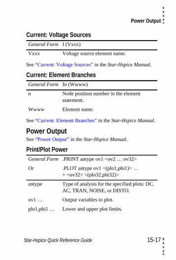
Power Output
Current: Voltage Sources
See“Current: Voltage Sources” in theStar-Hspice Manual.
Current: Element Branches
See“Current: Element Branches” in theStar-Hspice Manual.
Power OutputSee“Power Output” in theStar-Hspice Manual.
Print/Plot Power
General Form I (Vxxx)
Vxxx Voltage source element name.
General Form In (Wwww)
n Node position number in the elementstatement.
Wwww Element name.
General Form .PRINT antype ov1 <ov2 … ov32>
Or .PLOT antype ov1 <(plo1,phi1)> …+ <ov32> <(plo32,phi32)>
antype Type of analysis for the specified plots: DC,AC, TRAN, NOISE, or DISTO.
ov1 … Output variables to plot.
plo1,phi1 … Lower and upper plot limits.
Star-Hspice Quick Reference Guide 15-17
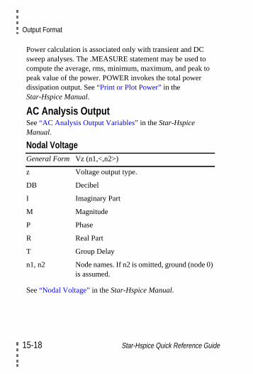
Output Format
oto
)
Power calculation is associated only with transient and DCsweep analyses. The .MEASURE statement may be used tcompute the average, rms, minimum, maximum, and peak peak value of the power. POWER invokes the total powerdissipation output. See“Print or Plot Power” in theStar-Hspice Manual.
AC Analysis OutputSee“AC Analysis Output Variables” in theStar-HspiceManual.
Nodal Voltage
See“Nodal Voltage” in theStar-Hspice Manual.
General Form Vz (n1,<,n2>)
z Voltage output type.
DB Decibel
I Imaginary Part
M Magnitude
P Phase
R Real Part
T Group Delay
n1, n2 Node names. If n2 is omitted, ground (node 0is assumed.
15-18 Star-Hspice Quick Reference Guide
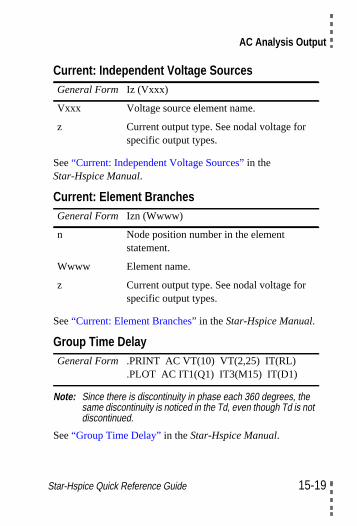
AC Analysis Output
Current: Independent Voltage Sources
See“Current: Independent Voltage Sources” in theStar-Hspice Manual.
Current: Element Branches
See“Current: Element Branches” in theStar-Hspice Manual.
Group Time Delay
Note: Since there is discontinuity in phase each 360 degrees, thesame discontinuity is noticed in the Td, even though Td is notdiscontinued.
See“Group Time Delay” in theStar-Hspice Manual.
General Form Iz (Vxxx)
Vxxx Voltage source element name.
z Current output type. See nodal voltage forspecific output types.
General Form Izn (Wwww)
n Node position number in the elementstatement.
Wwww Element name.
z Current output type. See nodal voltage forspecific output types.
General Form .PRINT AC VT(10) VT(2,25) IT(RL).PLOT AC IT1(Q1) IT3(M15) IT(D1)
Star-Hspice Quick Reference Guide 15-19
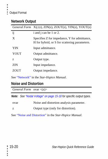
Output Format
Network Output
See“Network” in theStar-Hspice Manual.
Noise and Distortion
Note: See “Nodal Voltage” on page 15-18 for specific output types.
See“Noise and Distortion” in theStar-Hspice Manual.
General Form Xij (z), ZIN(z), ZOUT(z), YIN(z), YOUT(z)
ij i and j can be 1 or 2.
X Specifies Z for impedance, Y for admittance,H for hybrid, or S for scattering parameters.
YIN Input admittance.
YOUT Output admittance.
z Output type.
ZIN Input impedance.
ZOUT Output impedance.
General Form ovar <(z)>
ovar Noise and distortion analysis parameter.
z Output type (only for distortion).
15-20 Star-Hspice Quick Reference Guide
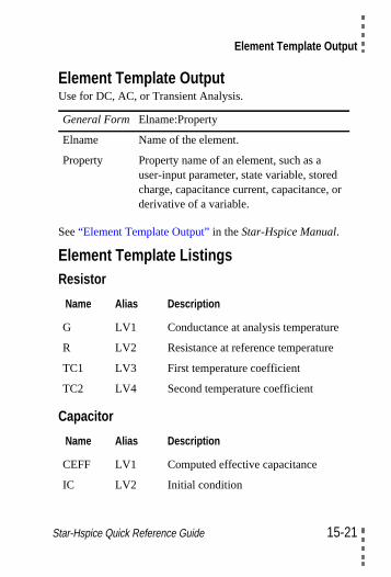
Element Template Output
r
Element Template OutputUse for DC, AC, or Transient Analysis.
See“Element Template Output” in theStar-Hspice Manual.
Element Template ListingsResistor
Capacitor
General Form Elname:Property
Elname Name of the element.
Property Property name of an element, such as auser-input parameter, state variable, storedcharge, capacitance current, capacitance, oderivative of a variable.
Name Alias Description
G LV1 Conductance at analysis temperature
R LV2 Resistance at reference temperature
TC1 LV3 First temperature coefficient
TC2 LV4 Second temperature coefficient
Name Alias Description
CEFF LV1 Computed effective capacitance
IC LV2 Initial condition
Star-Hspice Quick Reference Guide 15-21
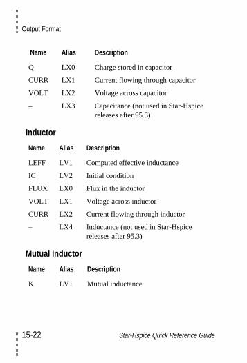
Output Format
Inductor
Mutual Inductor
Q LX0 Charge stored in capacitor
CURR LX1 Current flowing through capacitor
VOLT LX2 Voltage across capacitor
– LX3 Capacitance (not used in Star-Hspicereleases after 95.3)
Name Alias Description
LEFF LV1 Computed effective inductance
IC LV2 Initial condition
FLUX LX0 Flux in the inductor
VOLT LX1 Voltage across inductor
CURR LX2 Current flowing through inductor
– LX4 Inductance (not used in Star-Hspicereleases after 95.3)
Name Alias Description
K LV1 Mutual inductance
Name Alias Description
15-22 Star-Hspice Quick Reference Guide
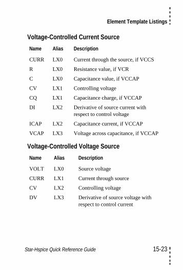
Element Template Listings
Voltage-Controlled Current Source
Voltage-Controlled Voltage Source
Name Alias Description
CURR LX0 Current through the source, if VCCS
R LX0 Resistance value, if VCR
C LX0 Capacitance value, if VCCAP
CV LX1 Controlling voltage
CQ LX1 Capacitance charge, if VCCAP
DI LX2 Derivative of source current withrespect to control voltage
ICAP LX2 Capacitance current, if VCCAP
VCAP LX3 Voltage across capacitance, if VCCAP
Name Alias Description
VOLT LX0 Source voltage
CURR LX1 Current through source
CV LX2 Controlling voltage
DV LX3 Derivative of source voltage withrespect to control current
Star-Hspice Quick Reference Guide 15-23
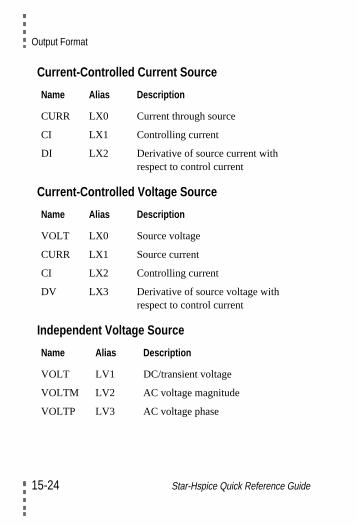
Output Format
Current-Controlled Current Source
Current-Controlled Voltage Source
Independent Voltage Source
Name Alias Description
CURR LX0 Current through source
CI LX1 Controlling current
DI LX2 Derivative of source current withrespect to control current
Name Alias Description
VOLT LX0 Source voltage
CURR LX1 Source current
CI LX2 Controlling current
DV LX3 Derivative of source voltage withrespect to control current
Name Alias Description
VOLT LV1 DC/transient voltage
VOLTM LV2 AC voltage magnitude
VOLTP LV3 AC voltage phase
15-24 Star-Hspice Quick Reference Guide
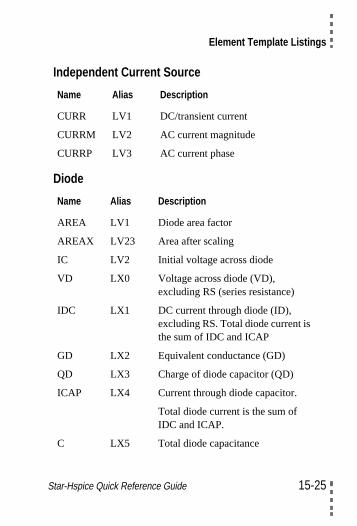
Element Template Listings
Independent Current Source
Diode
Name Alias Description
CURR LV1 DC/transient current
CURRM LV2 AC current magnitude
CURRP LV3 AC current phase
Name Alias Description
AREA LV1 Diode area factor
AREAX LV23 Area after scaling
IC LV2 Initial voltage across diode
VD LX0 Voltage across diode (VD),excluding RS (series resistance)
IDC LX1 DC current through diode (ID),excluding RS. Total diode current isthe sum of IDC and ICAP
GD LX2 Equivalent conductance (GD)
QD LX3 Charge of diode capacitor (QD)
ICAP LX4 Current through diode capacitor.
Total diode current is the sum ofIDC and ICAP.
C LX5 Total diode capacitance
Star-Hspice Quick Reference Guide 15-25
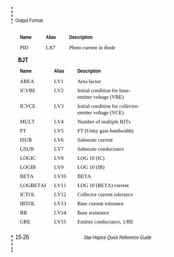
Output Format
BJT
PID LX7 Photo current in diode
Name Alias Description
AREA LV1 Area factor
ICVBE LV2 Initial condition for base-emitter voltage (VBE)
ICVCE LV3 Initial condition for collector-emitter voltage (VCE)
MULT LV4 Number of multiple BJTs
FT LV5 FT (Unity gain bandwidth)
ISUB LV6 Substrate current
GSUB LV7 Substrate conductance
LOGIC LV8 LOG 10 (IC)
LOGIB LV9 LOG 10 (IB)
BETA LV10 BETA
LOGBETAI LV11 LOG 10 (BETA) current
ICTOL LV12 Collector current tolerance
IBTOL LV13 Base current tolerance
RB LV14 Base resistance
GRE LV15 Emitter conductance, 1/RE
Name Alias Description
15-26 Star-Hspice Quick Reference Guide
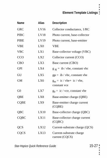
Element Template Listings
GRC LV16 Collector conductance, 1/RC
PIBC LV18 Photo current, base-collector
PIBE LV19 Photo current, base-emitter
VBE LX0 VBE
VBC LX1 Base-collector voltage (VBC)
CCO LX2 Collector current (CCO)
CBO LX3 Base current (CBO)
GPI LX4 g = ib / vbe, constant vbc
GU LX5 gµ = ib / vbc, constant vbe
GM LX6 gm = ic / vbe+ ic / vbe,
constant vce
G0 LX7 g0 = ic / vce, constant vbe
QBE LX8 Base-emitter charge (QBE)
CQBE LX9 Base-emitter charge current(CQBE)
QBC LX10 Base-collector charge (QBC)
CQBC LX11 Base-collector charge current(CQBC)
QCS LX12 Current-substrate charge (QCS)
CQCS LX13 Current-substrate chargecurrent (CQCS)
Name Alias Description
π
Star-Hspice Quick Reference Guide 15-27
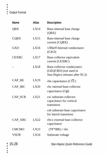
Output Format
QBX LX14 Base-internal base charge(QBX)
CQBX LX15 Base-internal base chargecurrent (CQBX)
GXO LX16 1/Rbeff Internal conductance(GXO)
CEXBC LX17 Base-collector equivalentcurrent (CEXBC)
– LX18 Base-collector conductance(GEQCBO) (not used inStar-Hspice releases after 95.3)
CAP_BE LX19 cbe capacitance (C )
CAP_IBC LX20 cbc internal base-collector
capacitance (Cµ)
CAP_SCB LX21 csc substrate-collectorcapacitance for verticaltransistors
csb substrate-base capacitancefor lateral transistors
CAP_XBC LX22 cbcx external base-collectorcapacitance
CMCMO LX23 (TF*IBE) / vbc
VSUB LX24 Substrate voltage
Name Alias Description
Π
15-28 Star-Hspice Quick Reference Guide
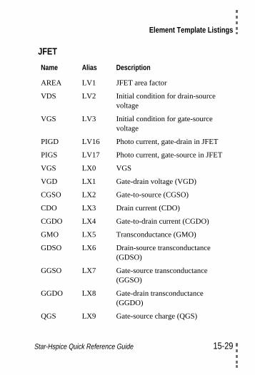
Element Template Listings
JFET
Name Alias Description
AREA LV1 JFET area factor
VDS LV2 Initial condition for drain-sourcevoltage
VGS LV3 Initial condition for gate-sourcevoltage
PIGD LV16 Photo current, gate-drain in JFET
PIGS LV17 Photo current, gate-source in JFET
VGS LX0 VGS
VGD LX1 Gate-drain voltage (VGD)
CGSO LX2 Gate-to-source (CGSO)
CDO LX3 Drain current (CDO)
CGDO LX4 Gate-to-drain current (CGDO)
GMO LX5 Transconductance (GMO)
GDSO LX6 Drain-source transconductance(GDSO)
GGSO LX7 Gate-source transconductance(GGSO)
GGDO LX8 Gate-drain transconductance(GGDO)
QGS LX9 Gate-source charge (QGS)
Star-Hspice Quick Reference Guide 15-29
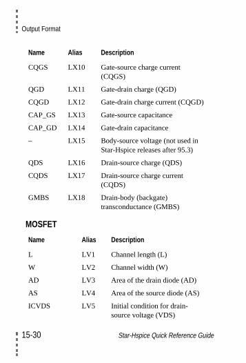
Output Format
MOSFET
CQGS LX10 Gate-source charge current(CQGS)
QGD LX11 Gate-drain charge (QGD)
CQGD LX12 Gate-drain charge current (CQGD)
CAP_GS LX13 Gate-source capacitance
CAP_GD LX14 Gate-drain capacitance
– LX15 Body-source voltage (not used inStar-Hspice releases after 95.3)
QDS LX16 Drain-source charge (QDS)
CQDS LX17 Drain-source charge current(CQDS)
GMBS LX18 Drain-body (backgate)transconductance (GMBS)
Name Alias Description
L LV1 Channel length (L)
W LV2 Channel width (W)
AD LV3 Area of the drain diode (AD)
AS LV4 Area of the source diode (AS)
ICVDS LV5 Initial condition for drain-source voltage (VDS)
Name Alias Description
15-30 Star-Hspice Quick Reference Guide
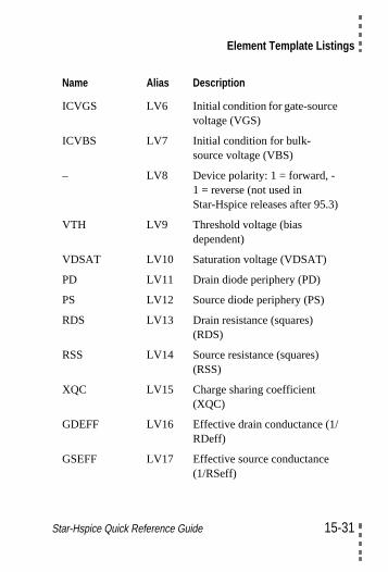
Element Template Listings
ICVGS LV6 Initial condition for gate-sourcevoltage (VGS)
ICVBS LV7 Initial condition for bulk-source voltage (VBS)
– LV8 Device polarity: 1 = forward, -1 = reverse (not used inStar-Hspice releases after 95.3)
VTH LV9 Threshold voltage (biasdependent)
VDSAT LV10 Saturation voltage (VDSAT)
PD LV11 Drain diode periphery (PD)
PS LV12 Source diode periphery (PS)
RDS LV13 Drain resistance (squares)(RDS)
RSS LV14 Source resistance (squares)(RSS)
XQC LV15 Charge sharing coefficient(XQC)
GDEFF LV16 Effective drain conductance (1/RDeff)
GSEFF LV17 Effective source conductance(1/RSeff)
Name Alias Description
Star-Hspice Quick Reference Guide 15-31

Output Format
IDBS LV18 Drain-bulk saturation current at-1 volt bias
ISBS LV19 Source-bulk saturation currentat -1 volt bias
VDBEFF LV20 Effective drain bulk voltage
BETAEFF LV21 BETA effective
GAMMAEFF LV22 GAMMA effective
DELTAL LV23 L (MOS6 amount of channellength modulation) (only validfor LEVELs 1, 2, 3 and 6)
UBEFF LV24 UB effective (only valid forLEVELs 1, 2, 3 and 6)
VG LV25 VG drive (only valid forLEVELs 1, 2, 3 and 6)
VFBEFF LV26 VFB effective
– LV31 Drain current tolerance (notused in Star-Hspice releasesafter 95.3)
IDSTOL LV32 Source diode current tolerance
IDDTOL LV33 Drain diode current tolerance
COVLGS LV36 Gate-source overlapcapacitance
Name Alias Description
∆
15-32 Star-Hspice Quick Reference Guide
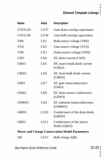
Element Template Listings
COVLGD LV37 Gate-drain overlap capacitance
COVLGB LV38 Gate-bulk overlap capacitance
VBS LX1 Bulk-source voltage (VBS)
VGS LX2 Gate-source voltage (VGS)
VDS LX3 Drain-source voltage (VDS)
CDO LX4 DC drain current (CDO)
CBSO LX5 DC source-bulk diode current(CBSO)
CBDO LX6 DC drain-bulk diode current(CBDO)
GMO LX7 DC gate transconductance(GMO)
GDSO LX8 DC drain-source conductance(GDSO)
GMBSO LX9 DC substrate transconductance(GMBSO)
GBDO LX10 Conductance of the drain diode(GBDO)
GBSO LX11 Conductance of the sourcediode (GBSO)
Meyer and Charge Conservation Model Parameters
QB LX12 Bulk charge (QB)
Name Alias Description
Star-Hspice Quick Reference Guide 15-33
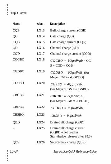
Output Format
CQB LX13 Bulk charge current (CQB)
QG LX14 Gate charge (QG)
CQG LX15 Gate charge current (CQG)
QD LX16 Channel charge (QD)
CQD LX17 Channel charge current (CQD)
CGGBO LX18 = CG
S + CGD + CGB
CGDBO LX19 , (for
Meyer CGD = -CGDBO)
CGSBO LX20 ,
(for Meyer CGS = -CGSBO)
CBGBO LX21 ,
(for Meyer CGB = -CBGBO)
CBDBO LX22
CBSBO LX23
QBD LX24 Drain-bulk charge (QBD)
– LX25 Drain-bulk charge current(CQBD) (not used inStar-Hspice releases after 95.3)
QBS LX26 Source-bulk charge (QBS)
Name Alias Description
CGGBO Qg/ Vgb∂∂=
CGDBO Qg/ Vdb∂∂=
CGSBO Qg/ Vsb∂∂=
CBGBO Qb/ Vgb∂∂=
CBDBO Qb/ Vdb∂∂=
CBSBO Qb/ Vsb∂∂=
15-34 Star-Hspice Quick Reference Guide
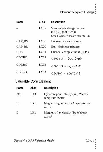
Element Template Listings
Saturable Core Element
– LX27 Source-bulk charge current(CQBS) (not used inStar-Hspice releases after 95.3)
CAP_BS LX28 Bulk-source capacitance
CAP_BD LX29 Bulk-drain capacitance
CQS LX31 Channel charge current (CQS)
CDGBO LX32
CDDBO LX33
CDSBO LX34
Name Alias Description
MU LX0 Dynamic permeability (mu) Weber/(amp-turn-meter)
H LX1 Magnetizing force (H) Ampere-turns/meter
B LX2 Magnetic flux density (B) Webers/
meter2
Name Alias Description
CDGBO Qd/ Vgb∂∂=
CDDBO Qd/ Vdb∂∂=
CDSBO Qd/ Vsb∂∂=
Star-Hspice Quick Reference Guide 15-35
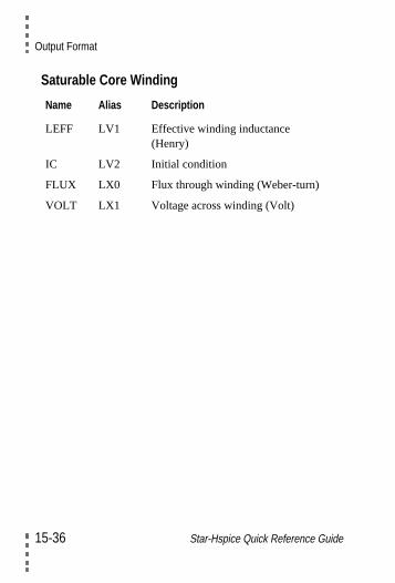
Output Format
Saturable Core Winding
Name Alias Description
LEFF LV1 Effective winding inductance(Henry)
IC LV2 Initial condition
FLUX LX0 Flux through winding (Weber-turn)
VOLT LX1 Voltage across winding (Volt)
15-36 Star-Hspice Quick Reference Guide