Stanford University Integrated Circuitssmirc.stanford.edu/papers/mtts98s-tom.pdf · T. Lee, Paul G....
48
T. Lee, Paul G. Allen Center for Integrated Systems Recent Developments in CMOS RF Integrated Circuits Recent Developments in CMOS RF Integrated Circuits Prof. Thomas H. Lee Stanford University [email protected] http://www-smirc.stanford.edu
Transcript of Stanford University Integrated Circuitssmirc.stanford.edu/papers/mtts98s-tom.pdf · T. Lee, Paul G....

T. Lee, Paul G. Allen Center for Integrated Systems
Recent Developments in CMOS RF Integrated Circuits
Recent Developments in CMOS RF
Integrated Circuits
Prof. Thomas H. LeeStanford University
[email protected]://www-smirc.stanford.edu

T. Lee, Paul G. Allen Center for Integrated Systems
Recent Developments in CMOS RF Integrated Circuits
Introduction
Digital CMOS is hardly the ideal medium for RF ICs. But is it hopelessly inferior?
Interesting question: How well can one do in such a technology if one tries very hard?
Scaling delivers faster devices every year; eventually, they’ll be fast enough.
Is the substrate really so big a problem that good inductors (and capacitors) simply cannot be realized?
Is device noise so large that CMOS LNAs will always be HNAs?
Does the inferior 1/f noise of CMOS transistors doom the close-in phase noise performance of oscillators?
Can you
really
build credible RF ICs in standard digital CMOS?

T. Lee, Paul G. Allen Center for Integrated Systems
Recent Developments in CMOS RF Integrated Circuits
Outline
A few brief words on scaling trends
The patterned ground shield spiral inductor
Capacitors
Fractal capacitors
Accumulation mode varactors
Passive mixers
Broadband noise models for the deep submicron regime
Power-constrained LNA design
A new phase noise theory and its implications for 1/f noise upconversion
Putting it all together: A 115mW single chip GPS receiv-er in 0.5
µ
m CMOS

T. Lee, Paul G. Allen Center for Integrated Systems
Recent Developments in CMOS RF Integrated Circuits
Scaling Trends in Brief
CMOS f
T
(and f
max
) are in the range of 30GHz now, and double roughly every three years.
Devices with ~75
n
m L
eff
have been demonstrated, and exhibit ~150GHz f
T
!
CMOS suffers from large source/drain parasitics, com-pared with other technologies.
Gate-drain “overlap” capacitance is also large.
Series gate resistance is also an increasingly serious problem as gate lengths continue to shrink, but can be accommodated by using narrower unit devices.
Salicided gates help, too.
Interconnect layers increasing at ~0.75 to 1 level per gen-eration (5 layers are now relatively common).

T. Lee, Paul G. Allen Center for Integrated Systems
Recent Developments in CMOS RF Integrated Circuits
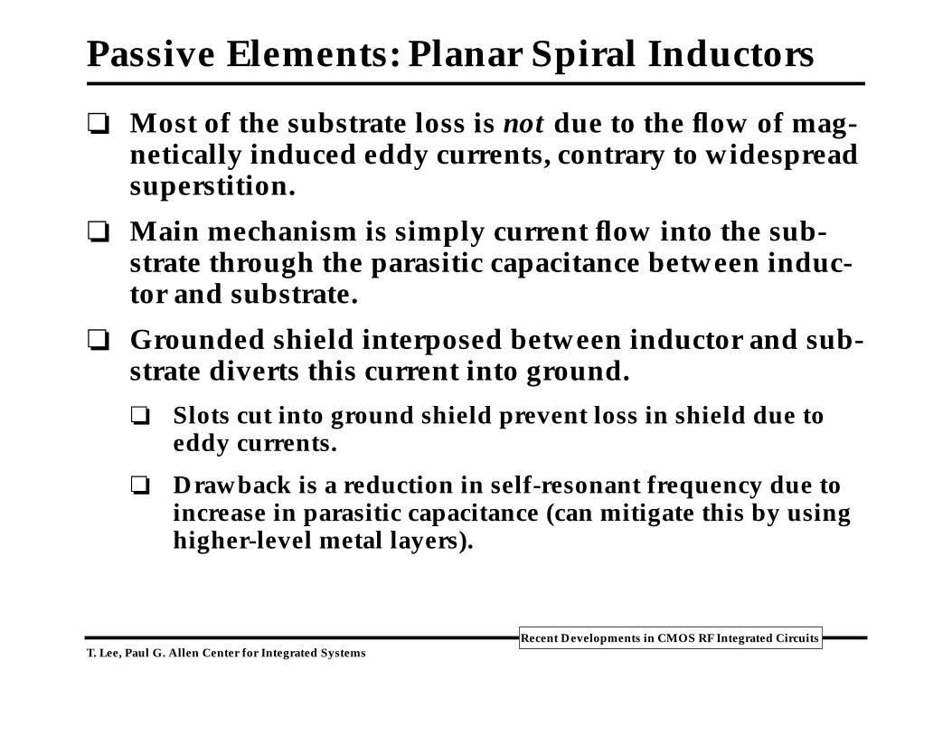
Passive Elements: Planar Spiral Inductors
Planar spirals in Si technology are infamous for poor Q (typically well below 10).
Conductor resistance, exacerbated by skin and proximi-ty effects, typically accounts for about half the loss.
Applies to both bulk and epi technologies.
The remaining loss is primarily due to currents flowing in the substrate.
Getting rid of the substrate would work wonders (e.g., post-fab etch, SOA, etc.), but requires deviation from ordinary process technology.
Next-best choice is to use a high-resistivity substrate, but can’t do so without sacrificing other CMOS characteristics.
Next next-best choice is to construct a
pseudo-substrate
out of existing interconnect layers.
T. Lee, Paul G. Allen Center for Integrated Systems
Recent Developments in CMOS RF Integrated Circuits
Passive Elements: Planar Spiral Inductors
Most of the substrate loss is
not
due to the flow of mag-netically induced eddy currents, contrary to widespread superstition.
Main mechanism is simply current flow into the sub-strate through the parasitic capacitance between induc-tor and substrate.
Grounded shield interposed between inductor and sub-strate diverts this current into ground.
Slots cut into ground shield prevent loss in shield due to eddy currents.
Drawback is a reduction in self-resonant frequency due to increase in parasitic capacitance (can mitigate this by using higher-level metal layers).
http://holst.stanford.edu/~CPYue [email protected]
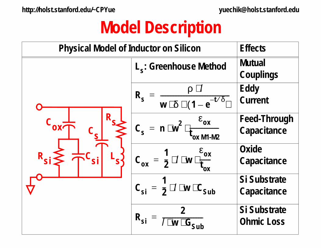
Model DescriptionPhysical Model of Inductor on Silicon Effects
MutualCouplingsEddy Current
Feed-Through Capacitance
Oxide Capacitance
Si SubstrateCapacitance
Si SubstrateOhmic Loss
Ls: Greenhouse Method
Rsρ l⋅
w δ 1 e t– δ⁄–( )⋅⋅
-------------------------------------------=
Cs n w2 εoxtox M1-M2------------------⋅ ⋅=
Cox12-- l w
εoxtox-------⋅ ⋅ ⋅=
Csi12-- l w CSub⋅ ⋅ ⋅=
Rsi2
l w GSub⋅ ⋅-------------------------=
Rs
Ls
Cs
Csi
Cox
Rsi

http://holst.stanford.edu/~CPYue [email protected]
Contour Plots of Q
21
53
79
4
4
5
4
79
1.6 GHz 3.0 GHz
Measured Q4.06.1
Measured Q5.24.0
0 100 200 300 400Outer Dimension (µm)
0 100 200 300 400Outer Dimension (µm)
0
2
4
6
8
10
Indu
ctan
ce (n
H)
1
http://holst.stanford.edu/~CPYue [email protected]
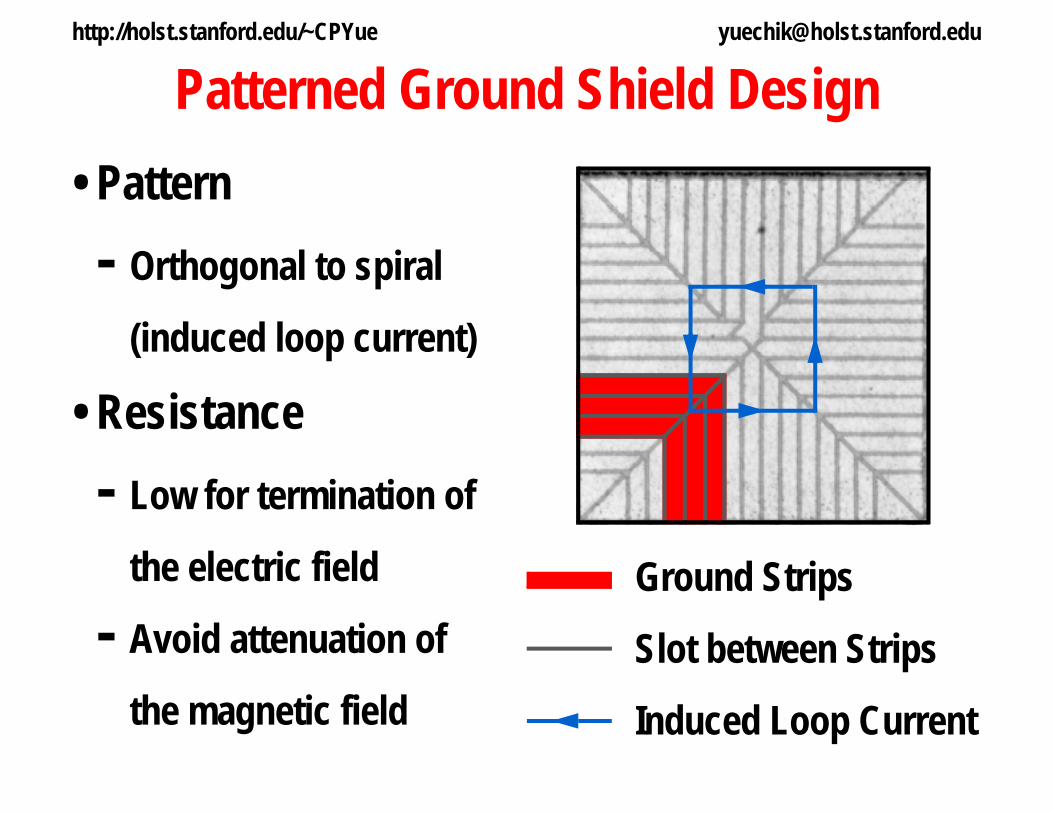
• Pattern
- Orthogonal to spiral
(induced loop current)
• Resistance
- Low for termination of
the electric field
- Avoid attenuation of
the magnetic field
Patterned Ground Shield Design
Ground Strips
Slot between Strips
Induced Loop Current

http://holst.stanford.edu/~CPYue [email protected]
Parallel LC Resonator at 2 GHz
PatternedPolysilicon
None(11 Ω-cm)
LC
QRESONATOR
fC∆f-----=
1.0 1.5 2.0 2.5 3.0Frequency (GHz)
0.00
0.25
0.50
0.75
1.00
1.25
1.50
Mag
nitu
de o
f Z (k
Ω)
Zmax at fc
∆f~30%

http://holst.stanford.edu/~CPYue [email protected]
Noise Coupling Measurement
PROBE
G
GS
G
GS
PROBE
HP 8720B
Probe Station

http://holst.stanford.edu/~CPYue [email protected]
Patterned
None (19 Ω-cm)
None(11 Ω-cm)
Probes up
0.1 1 10Frequency (GHz)
-90
-80
-70
-60
-50
-40
|s21
| (dB
)Effect of Polysilicon GS on Isolation
T. Lee, Paul G. Allen Center for Integrated Systems
Recent Developments in CMOS RF Integrated Circuits
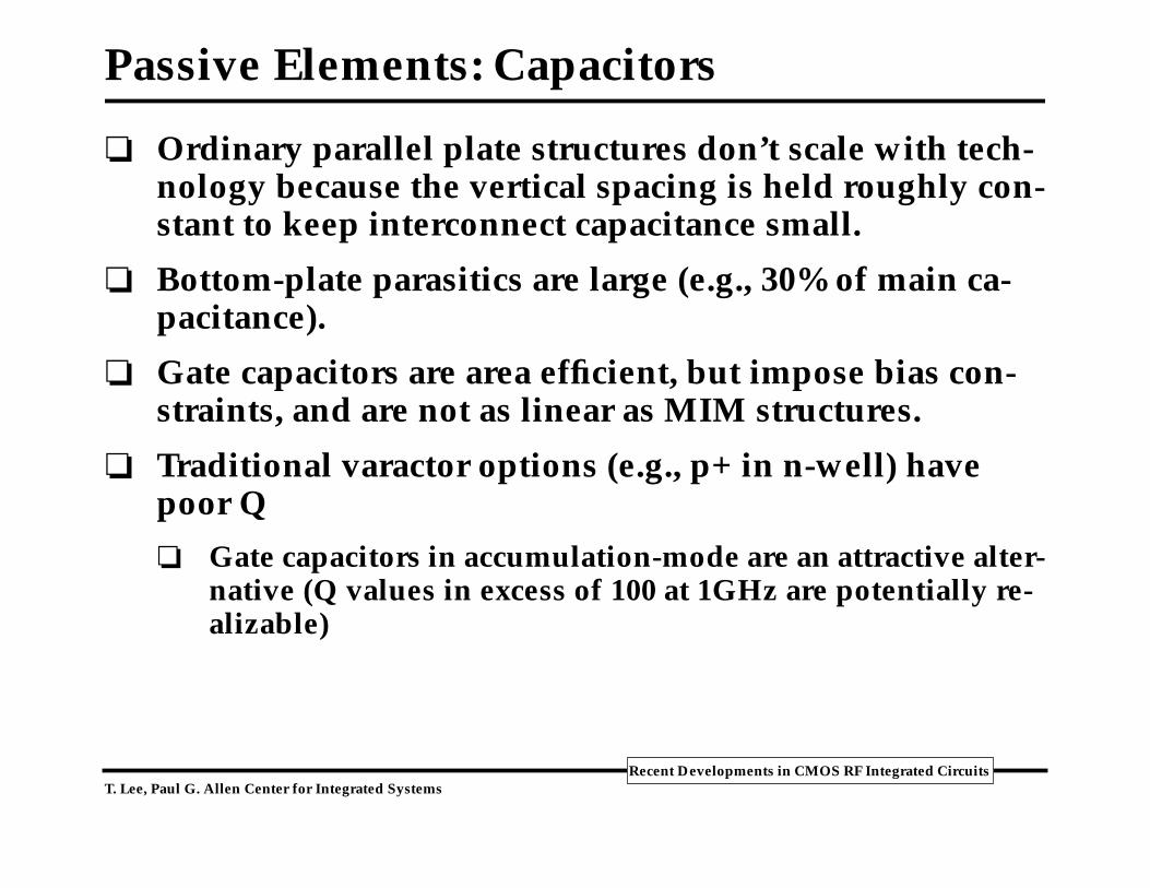
Passive Elements: Capacitors
Ordinary parallel plate structures don’t scale with tech-nology because the vertical spacing is held roughly con-stant to keep interconnect capacitance small.
Bottom-plate parasitics are large (e.g., 30% of main ca-pacitance).
Gate capacitors are area efficient, but impose bias con-straints, and are not as linear as MIM structures.
Traditional varactor options (e.g., p+ in n-well) have poor Q
Gate capacitors in accumulation-mode are an attractive alter-native (Q values in excess of 100 at 1GHz are potentially re-alizable)

Vertical vs. Lateral Flux
Lateral flux increases the total amount of capacitance.

Reduction of the Bottom-Plate Capacitance
First Terminal
First Terminal
Substrate
Second Terminal
Second Terminal
Area is smaller.
Some of the field lines terminate on the adjacentplate instead of the substrate.

Die Micrograph
Horizontal spacing=0.6 µmVertical spacing=0.8µmArea=24,000 µm2

Boost Factor vs. Lateral Spacing
0.1110
Minimum horizontal spacing (µm)
0.0
5.0
10.0
15.0
20.0C
tota
l/ C
para
llel
D=1.8D=1.6
0.6
Fabricatedfractal
2.3
Vertical metal spacing=0.8 µm
Area=24000 µm2
Metal thickness=0.8 µm
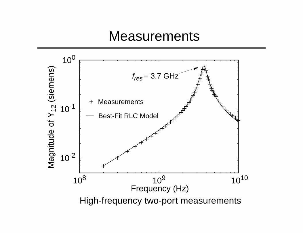
High-frequency two-port measurements
Measurements
108 109 1010
Frequency (Hz)
10-2
10-1
100M
agni
tude
of Y
12 (
siem
ens)
Measurements
Best-Fit RLC Model
+
fres = 3.7 GHz

rs C Ls
CbC 5.5pF=
Cb 0.3pF=
Cb
Ls 0.34nH=
r s 1.3Ω=
Measurements
Best-Fit Parameters

T. Lee, Paul G. Allen Center for Integrated Systems
Recent Developments in CMOS RF Integrated Circuits
Passive Elements: Capacitors
Accumulation-mode varactor (ref. Soorapanth et al., VLSI Circuits Symposium, June 1998):
Compatible with standard CMOS processing
Practical capacitance range exceeds 150%
n-well
n+ n+
p-substrate

T. Lee, Paul G. Allen Center for Integrated Systems
Recent Developments in CMOS RF Integrated Circuits
Passive Mixers
Gilbert multiplier performs mixing in current domain because bipolar transistors are not good voltage switch-es.
Penalty: V-I conversion costs power and linearity
CMOS voltage switches are excellent, so mixers made out of them work well:
@1.6GHz: 3.6dB loss, +10dBm IIP3 achieved at 200
µ
W
LO LO
LOLO
vIF

Stanford University
Simple CMOS Noise Model
vg2 Rg Cgd
Cgs rovgs
+
_gmvgs id2
ChannelThermal Noise
• Channel thermal noise is dominant.
• Gate resistance minimized by good layout.i kTB gd d
204= γ

Stanford University
LNA Input Stage
ZinLg
Ls
M1
M2Vbias
( )Z s L LsC
g
CL Lin s g
gs
m
gss T s= + + +
≈
1ω
( )G g Qg
C R L
RL
R
R
m eff m inm
gs s T s
T
sT s
s
T
s
, = =+
=+
=
11
12
ω ω
ω
ωω
ωω
Note: Gm,eff is independent of gm1!

Stanford University
Induced Gate Effects
S D
G
Vgs
Vds
Ig
• Gate Noise Current• Real Component of Zg
Stanford University
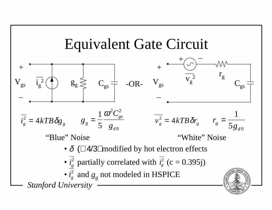
Equivalent Gate Circuit
vg2
ig2 Cgsgg -OR- Cgs
rg
+
_
Vgs
+
_
Vgs
gC
gg
gs
d
=1
5
2 2
0
ωi kTB gg g
2 4= δ rgg
d
=1
5 0
v kTB rg g2 4= δ
“Blue” Noise “White” Noise• δ (∼ 4/3) modified by hot electron effects
• partially correlated with (c = 0.395j)
• and gg not modeled in HSPICE
+ _
ig2 id
2
ig2

T. Lee, Paul G. Allen Center for Integrated Systems
Recent Developments in CMOS RF Integrated Circuits
LNA Design Procedure
Select device width roughly equal to (500
µ
m-GHz)/f
0
(for a 50
Ω
system)
Adjust bias to obtain desired power dissipation
Keep V
DS
–V
DSAT
as small as practical to minimize hot-elec-tron effects (say, under half a volt or so)
Select source degeneration inductance (assuming equal-sized cascoding and main devices) according to:
Add enough gate inductance to bring input to resonance
Noise factor bound is 1 + 2.4(
γ
/
α
)(
ω
/
ω
T
), so scaling con-tinues to help directly
LS
RS 1 2 Cgd Cgs⁄( )+[ ]⋅
ωT
≈

CIRCUITS: LNA / MIXER
Vb
LOp LOm
RFm
IFA
Ibias
RFp
LNA Mixer
1550 1560 1570 1580 1590 1600Frequency (MHz)
2.0
2.2
2.4
2.6
2.8
3.0
Noi
se F
igur
e (d
B)
Measured LNA Noise Figure
NF = 2.4dB @ 1575MHz
Ibias = 4.9mA
Shahani, Shaeffer and Lee, ”A 12mW Wide Dynamic Range CMOS GPS Receiver,” ISSCC 1997

http://smirc.stanford.edu/papers/Orals98s-ali.pdf Email: [email protected]
C Li(t)δ t τ–( )
t
i(t)
t
Vout
t
Vout
Oscillators Are Time-Variant Systems
τ
Impulse injected at the peak of amplitude.
∆V
∆V
Even for an ideal LC oscillator, the phase response is Time Variant.
Impulse injected at zero crossing.τ
τ

http://smirc.stanford.edu/papers/Orals98s-ali.pdf Email: [email protected]
Phase Impulse Response
φ t( )hφ t τ,( )
0 t
i(t)
τ 0 τ
hφ t τ,( )Γ ωoτ( )
qmax-------------------u t τ–( )=
t
i t( )
The unit impulse response is:
Γ x( ) is a dimensionless function periodic in 2π, describing how much
phase change results from applying an impulse at time: t Tx
2π------=
The phase impulse response of an arbitrary oscillator is a time varying step.

http://smirc.stanford.edu/papers/Orals98s-ali.pdf Email: [email protected]
t
t
t
t
V out t( ) V out t( )
Γ ω0t( ) Γ ω0t( )
LC Oscillator Ring Oscillator
Impulse Sensitivity Function (ISF)
The ISF quantifies the sensitivity of every point in the waveform to perturbations.
Waveform
ISF

http://smirc.stanford.edu/papers/Orals98s-ali.pdf Email: [email protected]
φ t( ) hφ t τ,( )i τ( )dτ∞–
∞
∫1
qmax---------------- Γ ω0τ( )i τ( )dτ
∞–
t
∫= =
φ t( )i t( )hφ t τ,( )
Γ ω0τ( )
qmax-------------------u t τ–( )=
Superposition Integral:
Phase Response to an Arbitrary Source
Γ ω0t( )
∞–t
∫ ω0t φ t( )+[ ]cosi t( )
qmax----------------
φ t( )ψ t( ) V t( )
IdealIntegration
PhaseModulation
Equivalent representation:
http://smirc.stanford.edu/papers/Orals98s-ali.pdf Email: [email protected]
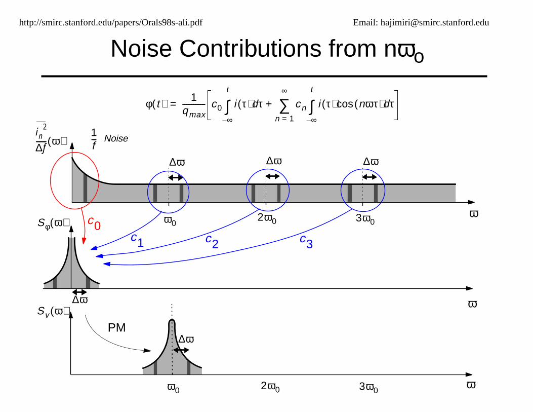
c0c1 c2 c3
2ω0ω0 3ω0ω
Sφ ω( )
i n2
∆f------- ω( )1f--- Noise
Sv ω( )
2ω0ω0 3ω0ω
ω
PM∆ω
∆ω ∆ω ∆ω
∆ω
Noise Contributions from nωo
φ t( ) 1qmax------------- c0 i τ( )dτ
∞–
t
∫ cn i τ( ) nωτ( )cos dτ∞–
t
∫n 1=
∞
∑+=

http://smirc.stanford.edu/papers/Orals98s-ali.pdf Email: [email protected]
c012π------ Γ x( )dx
0
2π
∫=
t
t
V out t( )
Γ ωt( )
Symmetric rise and fall time
t
t
V out t( )
Γ ωt( )
Asymmetric rise and fall time
Effect of Symmetry
The dc value of the ISF is governed by rise and fall time symmetry, and
controls the contribution of low frequency noise to the phase noise.

http://smirc.stanford.edu/papers/Orals98s-ali.pdf Email: [email protected]
1/f 3 Corner of Phase Noise Spectrum
ω1 f
3⁄ω1 f⁄
c0Γrms--------------
2
=
The 1/f3 corner of phase noise is NOT the same as 1/f corner of device noise
log(ω-ωo)
L ∆ω( )
1f 2-----
c0
c1
c2
c3
ω1f---
ω 1
f 3----
By designing for a symmetric waveform, the performancedegradation due to low frequency noise can be minimized.

http://smirc.stanford.edu/papers/Orals98s-ali.pdf Email: [email protected]
L
C
Vdd
A Symmetric LC Oscillator
Possible to Adjust Symmetry Properties of the Waveform
WN/L
WP/L
WN/L
WP/L
Adjust ratiosfor symmetry

http://smirc.stanford.edu/papers/Orals98s-ali.pdf Email: [email protected]
Complementary Cross-Coupled VCO
1.5
2
2.5
3
24
68
1012
1416
x 10−3
−126
−124
−122
−120
−118
−116
−114
−112
f0=1.8GHz, 0.25µm Process
Pha
se n
oise
bel
ow c
arrie
r at
600
kHz
offs
et
Vdd Itail (mA)
-121dBc/Hz@600kHz
f0=1.8GHz
P=6mW
CL
Vdd
bias
Gnd
Itail

GPS OVERVIEW: TYPICAL RECEIVER ARCHITECTURES
Distinguishing Features:
Typical on-chip PD
is 100mW – 500mW
Off-chip LNA oractive antenna
Off-chip IF filtering
1 or 2 bit quantization
PLL
Off-Chip
2
1- OR -
Dual-Conversion
2
PLL
Off-Chip
Single-Conversion

ARCHITECTURE: LOW-IF RECEIVER
Primary Goal: Make choices to minimize PD, maximize integration.
Low-IF) On-chipactive channel filter.
Image in GPS band )
Relaxed I/Q matching.
Eliminate PLL prescaler
) Saves power / noise.
1-bit quantizationfor simplicity.
BandGap
π/2
M*f0
N*f0
I[n]
Q[n]
PLL(M=17)
(N=23)
f0=4.024MHz
2.036MHz
Signal Path
1.57542GHz
APD
APD=1.573384GHzN*M*f0

CIRCUITS: IFA
Low input capacitance, high linearity.
Load resistors terminate the active filter input.
Inp InmM1
M3
Ibias
Outp
M4
M2Outm
Ibias
-0.2 -0.1 0.0 0.1 0.2DC Input Voltage (V)
-40
-30
-20
-10
0
10
20
30
Vol
tage
Gai
n (d
B)
Simulated IFA Voltage Gain

CIRCUITS: GM-C FILTER (TRANSCONDUCTOR)
Use two square-law transconductors to build a linear, class-AB transconductor.A little positive feedback (M10) compensates for mobility degradation in M1.
M2
M10
M1
M5Ibias
M6
Inp InmOutp Outm
-0.4 -0.3 -0.2 -0.1 0.0 0.1 0.2 0.3 0.4DC Input Voltage (V)
0.90
0.95
1.00
1.05
1.10
Rel
ativ
e G
m
Simulated Gyrator Transconductance
With Positive FB (M10)Without Positive FB+/- 10% M10 Variation

EXPERIMENTAL RESULTS: NOISE FIGURE
1.0 1.5 2.0 2.5 3.0 3.5 4.0IF Frequency (MHz)
3.0
6.0
9.0
12.0N
oise
Fig
ure
(dB
)
Coherent Receiver Spot Noise Figure(Pre-Limiter)
Fine Quantization1-bit Quantization

EXPERIMENTAL RESULTS: LINEARITY
-45 -40 -35 -30 -25 -20 -15 -10Input Power (dBm)
-80
-60
-40
-20
0
20
40O
utpu
t Vol
tage
(dB
Vrm
s)
Signal Path 3rd Order Intermodulation
Slope=3

EXPERIMENTAL RESULTS: BLOCKING PERFORMANCE
0 10 20 30 40 50 60Offset Frequency (MHz)
-60
-50
-40
-30
-20B
lock
ing
Sou
rce
Pow
er (
dBm
)
Receiver 1-dB Blocking De-Sensitization(No Front-End RF Filter)
INMARSATUplink Band
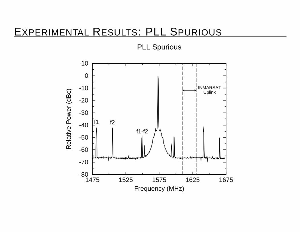
EXPERIMENTAL RESULTS: PLL SPURIOUS
1475 1525 1575 1625 1675Frequency (MHz)
-80
-70
-60
-50
-40
-30
-20
-10
0
10R
elat
ive
Pow
er (
dBc)
PLL Spurious
INMARSATUplink
f1 f2
f1-f2

PERFORMANCE SUMMARY
Signal Path Performance PLL PerformanceLNA Noise Figure 2.4dB Loop Bandwidth 5MHzLNA S11 -15dB Spurious Tones -42dBcCoherent Receiver NF 4.1dB VCO Tuning Range 240MHz ( 7.6%)IIP3 (Filter-limited) -16dBm @ -43dBm Ps VCO Gain Constant 240MHz/VPeak SFDR 57dB LO Leakage @ LNA < -53dBmFilter Cutoff Freq. 3.5MHzFilter PB Peaking 1dB Power/TechnologyFilter SB Atten. 52dB @ 8MHz Signal Path 79mW
68dB @ 10MHz PLL / VCO 36mWPre-FilterGp 19dB Supply Voltage 2.5VPre-FilterAv 32dBTotalGp 82dB Die Area 11.2mm2
TotalAv 107dB Technology 0.5m CMOSNon-Coherent Output SNR 15dB

T. Lee, Paul G. Allen Center for Integrated Systems
Recent Developments in CMOS RF Integrated Circuits
Closing Thoughts
CMOS is not ideal, but much more than adequate for many applications.
Scaling trends will continue to improve CMOS.
“RF CMOS” is not an oxymoron anymore.

T. Lee, Paul G. Allen Center for Integrated Systems
Recent Developments in CMOS RF Integrated Circuits
Acknowledgments
Many slides were prepared, and generously supplied, by the following Stanford Ph.D. candidates:
Hirad Samavati (fractal capacitors)
Patrick Yue (spiral inductors)
Ali Hajimiri (oscillator phase noise)
Derek Shaeffer and Arvin Shahani (LNA work and GPS receiver)