ST7781 SPEC V1.0 20090210 - Arm Mbed · 94 agnd -1820 -304 134 vcl 980 -304 95 agnd ... 175 c11n...
85
ST ST7781 262K Color Single –Chip TFT Controller/Driver 1. Introduction The ST7781 is a single-chip controller/driver for 262K-color, graphic type TFT-LCD. It consists of 720 source line and 320 gate line driving circuits. This chip is capable of connecting directly to an external microprocessor, and accepts, 8-bits/9-bits/16-bits/18-bits parallel interface. Display data can be stored in the on-chip display data RAM of 240x320x18 bits. It can perform display data RAM read/write operation with no external operation clock to minimize power consumption. In addition, because of the integrated power supply circuits necessary to drive liquid crystal, it is possible to make a display system with the fewest components. 2. Features Driver Output: - 720ch Source Outputs (240 X RGB) - 320ch Gate Outputs - Common Electrode Output Single Chip Display RAM: -Capacity: 240x320x18 bit Support Display Color - 65K Color - 262K Color - 8-color (Idle Mode) Supported LC Type Option - MVA LC Type - Transflective LC Type - Transmissive LC Type Supported MCU Interface - 8/9/16/18-bit Interface with 8080-Series MCU Display Features - Partial Display Mode - Resizing Function (x1/2, x1/4) Build-in Circuit - DC/DC Converter - Adjustable VCOM Generation - Oscillator for Display Clock Generation - Timing Controller - Non-volatile Memory for Factory Default Value - Line Inversion, Frame Inversion Non-Volatile Memory - 7-bits for ID Code - 5-bits for VCOM Adjustment Supply Voltage Range - Analog Supply Voltage (VDD) Range: 2.5V to 3.3V - I/O Supply Voltage (VDDI) Range: 1.65V to 3.3V Output Voltage Level - GVDD – AGND: 3V to (AVDD-0.5) V - AVDD – AGND: 4.5V to 5.6V - VCL – AGND: -2.0V to -3.0V - VCOMH – AGND: 3.0V to (AVDD-0.5) V - VCOML – AGND: (VCL+0.5) V to 0.0V - VGH – AGND: 10V to 16.5V - VGL – AGND: -5V to -14V Lower Power Consumption - CMOS Compatible Inputs - Optimized Layout for COG Assembly - Operate Temperature Range: -30 ℃ ~ +85℃ ST7781 8080 Parallel Interface :8bit/ 9 bit/16 bit /18bit Sitronix Technology Corp. reserves the right to change the contents in this document without prior notice.
-
Upload
phungkhanh -
Category
Documents
-
view
242 -
download
0
Transcript of ST7781 SPEC V1.0 20090210 - Arm Mbed · 94 agnd -1820 -304 134 vcl 980 -304 95 agnd ... 175 c11n...
ST
ST7781 262K Color Single –Chip TFT Controller/Driver
1. Introduction The ST7781 is a single-chip controller/driver for 262K-color, graphic type TFT-LCD. It consists of 720 source line and
320 gate line driving circuits. This chip is capable of connecting directly to an external microprocessor, and accepts, 8-bits/9-bits/16-bits/18-bits parallel interface. Display data can be stored in the on-chip display data RAM of 240x320x18 bits. It can perform display data RAM read/write operation with no external operation clock to minimize power consumption. In addition, because of the integrated power supply circuits necessary to drive liquid crystal, it is possible to make a display system with the fewest components.
2. Features � Driver Output:
- 720ch Source Outputs (240 X RGB) - 320ch Gate Outputs - Common Electrode Output
� Single Chip Display RAM:
-Capacity: 240x320x18 bit � Support Display Color
- 65K Color - 262K Color - 8-color (Idle Mode)
� Supported LC Type Option - MVA LC Type - Transflective LC Type - Transmissive LC Type
� Supported MCU Interface - 8/9/16/18-bit Interface with 8080-Series MCU
� Display Features - Partial Display Mode - Resizing Function (x1/2, x1/4)
� Build-in Circuit - DC/DC Converter - Adjustable VCOM Generation - Oscillator for Display Clock Generation - Timing Controller - Non-volatile Memory for Factory Default Value - Line Inversion, Frame Inversion
� Non-Volatile Memory
- 7-bits for ID Code - 5-bits for VCOM Adjustment
� Supply Voltage Range - Analog Supply Voltage (VDD) Range: 2.5V to 3.3V - I/O Supply Voltage (VDDI) Range: 1.65V to 3.3V
� Output Voltage Level - GVDD – AGND: 3V to (AVDD-0.5) V - AVDD – AGND: 4.5V to 5.6V - VCL – AGND: -2.0V to -3.0V - VCOMH – AGND: 3.0V to (AVDD-0.5) V - VCOML – AGND: (VCL+0.5) V to 0.0V - VGH – AGND: 10V to 16.5V - VGL – AGND: -5V to -14V
� Lower Power Consumption - CMOS Compatible Inputs - Optimized Layout for COG Assembly - Operate Temperature Range: -30 ℃ ~ +85℃
ST7781 8080 Parallel Interface :8bit/ 9 bit/16 bit /18bit
Sitronix Technology Corp. reserves the right to change the contents in this document without prior notice.
ST7781
Ver. 1.0 2
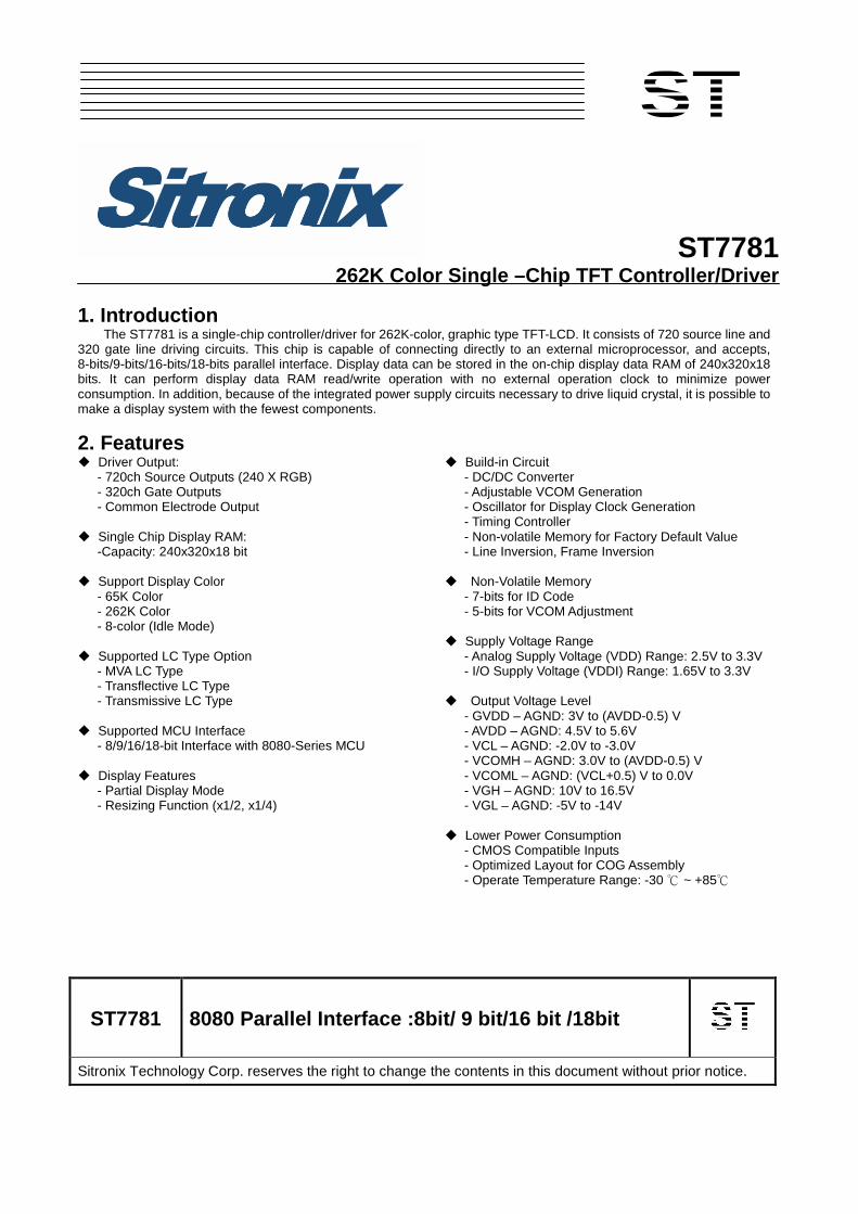
3. Pad Arrangement
Face Up
(Bump View)
C11PC11PC11PC11PVGLVGLVGLVGLVGLVGL
VGLVGLVGLVGL
AGNDAGNDAGNDVGHVGHVGH
VGHVGHVGH
DUMMYDUMMY
C21NC21NC21NC21NC21P
C21PC21PC21PC22NC22NC22NC22NC22NC22NC22N
C22PC22PC22PC22PC22PC22PC22PC23NC23NC23N
C23NC23NC23NC23NC23PC23PC23PC23PC23PC23P
C23PDUMMYDUMMY
10
20
30
40
50
60
70
80
90
100
110
120
130
140
150
160
170
180
190
200
210
220
230
Y
X
………
………
………
………
DUMMYG319G317G315G313G311G309G307G305G303
G 17G 15G 13G 11G 9G 7G 5G 3G 1DUMMYDUMMYS 1S 2S 3S 4S 5S 6S 7S 8S 9
S353S354S355S356S357S358S359S360DUMMY
DUMMYS361S362S363S364S365S366S367S368S369
S712S713S714S715S716S717S718S719S720DUMMYDUMMYG2G4G6G8G10G12G14G16G18
G304G306G308G310G312G314G316G318G320DUMMY
DUMMY1SW_EE
IOGNDDUMTESTO TESTO TESTO
IM0IM1IM2IM3
DUMMYTESTO TESTO TESTO TESTO TESTO TESTO TESTO RESETRESET
TESTITESTITESTITESTIDB17DB16DB15DB14DB13
TESTO
DB12DB11DB10DB9DB8
DUMMYTESTO
DB7DB6DB5
DB4DB3DB2DB1DB0
TESTO TESTOTESTI
/RD/WR
RS/CS
TESTO OSC
FMARKTESTO TESTOTESTOTESTOTESTO
TESTOTESTOTESTO TESTO TESTODUMMY
VDDIVDDIVDDIVDDI
VDDIVDDIVCCVCCVCCVCCVCCVCCVCCVCC
VCCVCCVCC
DUMMYDGNDDGNDDGNDDGNDDGNDDGND
DGNDDGNDAGNDAGNDAGNDAGNDAGNDAGNDAGNDAGND
AGNDAGNDAGNDAGND
V25DUMMYDUMMYVCOMVCOMVCOM
VCOMVCOMVCOMVCOM
VCOMHVCOMHVCOMHVCOMHVCOMHVCOMH
VCOMLVCOMLVCOMLVCOMLGVDDGVDDGVDD
DUMMYDUMMYDUMMY
VCLVCLVCLVCLVCL
AVDDAVDDAVDDAVDDAVDD
AVDDVCI1VCI1VCI1VDDVDDVDDVDDVDDVDD
VDDVDDVDDVDDVDDVDDVDDVDDVDDVDD
VDDVDD
TESTO TESTO C12NC12NC12NC12NC12NC12P
C12PC12PC12PC12PC11NC11NC11NC11NC11NC11P
Chip Size: 18163um x 800um
Chip Thickness : 280um or 300um (typ.)
Pad Location: Pad Center.
Coordinate Origin: Chip Center
Au Bump Height: 15um (typ.)
Au Bump Size:
1. 16um x 90umGate: G1 ~ G320Source: S1 ~ S720
2. 50um x 80umInput PadsPad 1 to 243.
10
10
15 20 15
15
15
20
15 20 15
10
10 15
15
20
Alignment Marks
Alignment Mark: A1 (X , Y) = (-8751 , 252.5)
Alignment Mark: A2 (X , Y) = (8751 , 252.5)
Bump View
ST7781
Ver. 1.0 3
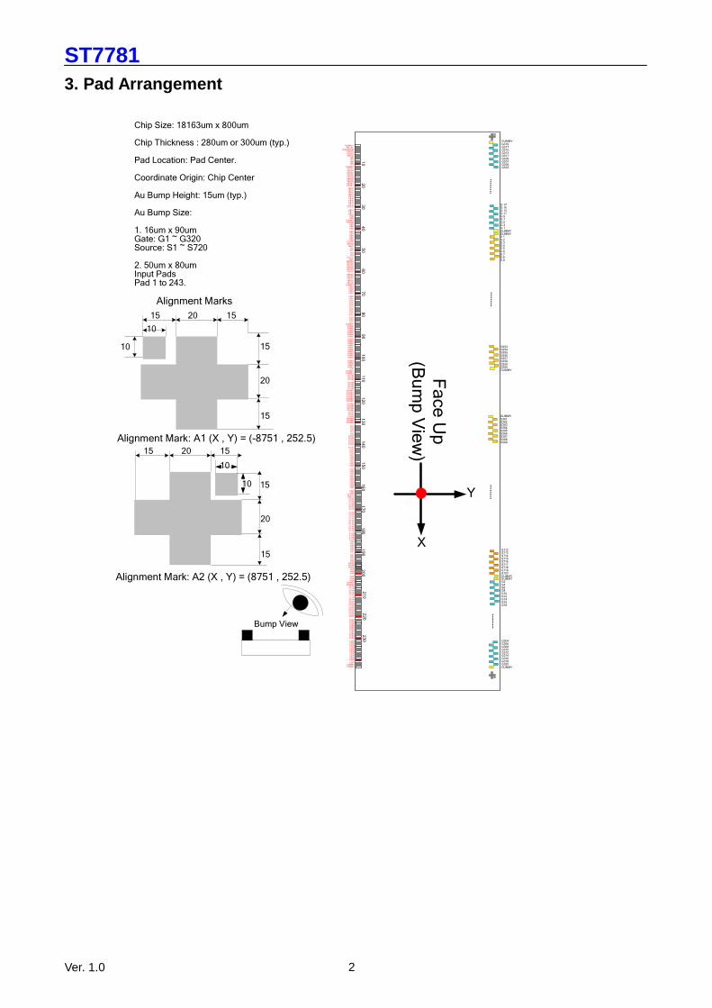
S1~S720 G1~G320 DUMMY
(No.244~1291)
I/O Pads (No.1~243)
ST7781
Ver. 1.0 4
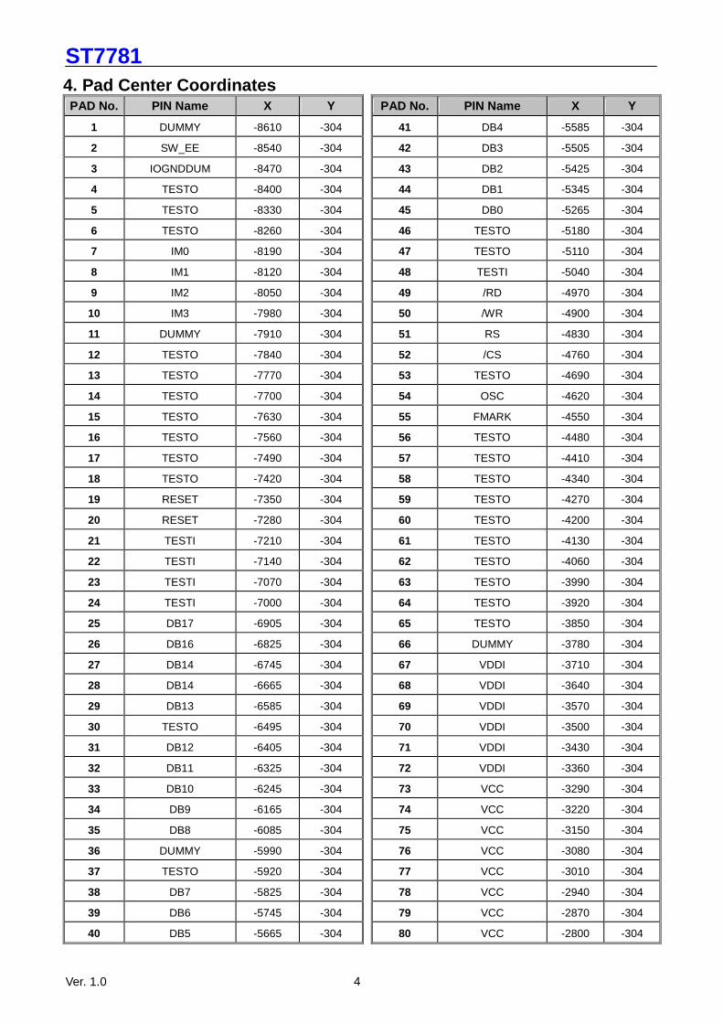
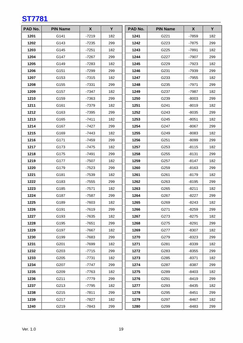
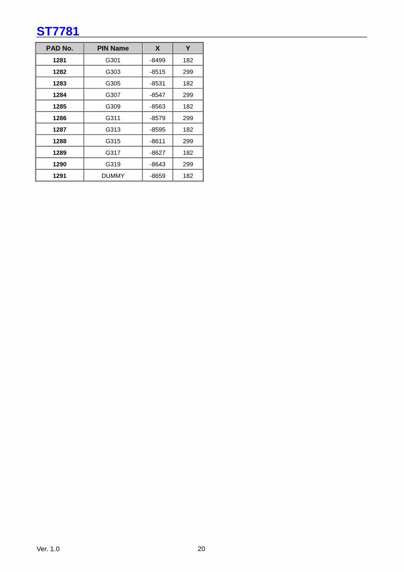
4. Pad Center Coordinates PAD No. PIN Name X Y PAD No. PIN Name X Y
1 DUMMY -8610 -304 41 DB4 -5585 -304
2 SW_EE -8540 -304 42 DB3 -5505 -304
3 IOGNDDUM -8470 -304 43 DB2 -5425 -304
4 TESTO -8400 -304 44 DB1 -5345 -304
5 TESTO -8330 -304 45 DB0 -5265 -304
6 TESTO -8260 -304 46 TESTO -5180 -304
7 IM0 -8190 -304 47 TESTO -5110 -304
8 IM1 -8120 -304 48 TESTI -5040 -304
9 IM2 -8050 -304 49 /RD -4970 -304
10 IM3 -7980 -304 50 /WR -4900 -304
11 DUMMY -7910 -304 51 RS -4830 -304
12 TESTO -7840 -304 52 /CS -4760 -304
13 TESTO -7770 -304 53 TESTO -4690 -304
14 TESTO -7700 -304 54 OSC -4620 -304
15 TESTO -7630 -304 55 FMARK -4550 -304
16 TESTO -7560 -304 56 TESTO -4480 -304
17 TESTO -7490 -304 57 TESTO -4410 -304
18 TESTO -7420 -304 58 TESTO -4340 -304
19 RESET -7350 -304 59 TESTO -4270 -304
20 RESET -7280 -304 60 TESTO -4200 -304
21 TESTI -7210 -304 61 TESTO -4130 -304
22 TESTI -7140 -304 62 TESTO -4060 -304
23 TESTI -7070 -304 63 TESTO -3990 -304
24 TESTI -7000 -304 64 TESTO -3920 -304
25 DB17 -6905 -304 65 TESTO -3850 -304
26 DB16 -6825 -304 66 DUMMY -3780 -304
27 DB14 -6745 -304 67 VDDI -3710 -304
28 DB14 -6665 -304 68 VDDI -3640 -304
29 DB13 -6585 -304 69 VDDI -3570 -304
30 TESTO -6495 -304 70 VDDI -3500 -304
31 DB12 -6405 -304 71 VDDI -3430 -304
32 DB11 -6325 -304 72 VDDI -3360 -304
33 DB10 -6245 -304 73 VCC -3290 -304
34 DB9 -6165 -304 74 VCC -3220 -304
35 DB8 -6085 -304 75 VCC -3150 -304
36 DUMMY -5990 -304 76 VCC -3080 -304
37 TESTO -5920 -304 77 VCC -3010 -304
38 DB7 -5825 -304 78 VCC -2940 -304
39 DB6 -5745 -304 79 VCC -2870 -304
40 DB5 -5665 -304 80 VCC -2800 -304
ST7781
Ver. 1.0 5
PAD No. PIN Name X Y PAD No. PIN Name X Y
81 VCC -2730 -304 121 VCOML 70 -304
82 VCC -2660 -304 122 VCOML 140 -304
83 VCC -2590 -304 123 VCOML 210 -304
84 DUMMY -2520 -304 124 VCOML 280 -304
85 DGND -2450 -304 125 GVDD 350 -304
86 DGND -2380 -304 126 GVDD 420 -304
87 DGND -2310 -304 127 GVDD 490 -304
88 DGND -2240 -304 128 DUMMY 560 -304
89 DGND -2170 -304 129 DUMMY 630 -304
90 DGND -2100 -304 130 DUMMY 700 -304
91 DGND -2030 -304 131 VCL 770 -304
92 DGND -1960 -304 132 VCL 840 -304
93 AGND -1890 -304 133 VCL 910 -304
94 AGND -1820 -304 134 VCL 980 -304
95 AGND -1750 -304 135 VCL 1050 -304
96 AGND -1680 -304 136 AVDD 1120 -304
97 AGND -1610 -304 137 AVDD 1190 -304
98 AGND -1540 -304 138 AVDD 1260 -304
99 AGND -1470 -304 139 AVDD 1330 -304
100 AGND -1400 -304 140 AVDD 1400 -304
101 AGND -1330 -304 141 AVDD 1470 -304
102 AGND -1260 -304 142 VCI1 1540 -304
103 AGND -1190 -304 143 VCI1 1610 -304
104 AGND -1120 -304 144 VCI1 1680 -304
105 V25 -1050 -304 145 VDD 1750 -304
106 DUMMY -980 -304 146 VDD 1820 -304
107 DUMMY -910 -304 147 VDD 1890 -304
108 VCOM -840 -304 148 VDD 1960 -304
109 VCOM -770 -304 149 VDD 2030 -304
110 VCOM -700 -304 150 VDD 2100 -304
111 VCOM -630 -304 151 VDD 2170 -304
112 VCOM -560 -304 152 VDD 2240 -304
113 VCOM -490 -304 153 VDD 2310 -304
114 VCOM -420 -304 154 VDD 2380 -304
115 VCOMH -350 -304 155 VDD 2450 -304
116 VCOMH -280 -304 156 VDD 2520 -304
117 VCOMH -210 -304 157 VDD 2590 -304
118 VCOMH -140 -304 158 VDD 2660 -304
119 VCOMH -70 -304 159 VDD 2730 -304
120 VCOMH 0 -304 160 VDD 2800 -304
ST7781
Ver. 1.0 6
PAD No. PIN Name X Y PAD No. PIN Name X Y
161 VDD 2870 -304 201 VGH 5670 -304
162 VDD 2940 -304 202 VGH 5740 -304
163 TESTO 3010 -304 203 VGH 5810 -304
164 TESTO 3080 -304 204 DUMMY 5880 -304
165 C12N 3150 -304 205 DUMMY 5950 -304
166 C12N 3220 -304 206 C21N 6020 -304
167 C12N 3290 -304 207 C21N 6090 -304
168 C12N 3360 -304 208 C21N 6160 -304
169 C12N 3430 -304 209 C21N 6230 -304
170 C12P 3500 -304 210 C21P 6300 -304
171 C12P 3570 -304 211 C21P 6370 -304
172 C12P 3640 -304 212 C21P 6440 -304
173 C12P 3710 -304 213 C21P 6510 -304
174 C12P 3780 -304 214 C22N 6580 -304
175 C11N 3850 -304 215 C22N 6650 -304
176 C11N 3920 -304 216 C22N 6720 -304
177 C11N 3990 -304 217 C22N 6790 -304
178 C11N 4060 -304 218 C22N 6860 -304
179 C11N 4130 -304 219 C22N 6930 -304
180 C11P 4200 -304 220 C22N 7000 -304
181 C11P 4270 -304 221 C22P 7070 -304
182 C11P 4340 -304 222 C22P 7140 -304
183 C11P 4410 -304 223 C22P 7210 -304
184 C11P 4480 -304 224 C22P 7280 -304
185 VGL 4550 -304 225 C22P 7350 -304
186 VGL 4620 -304 226 C22P 7420 -304
187 VGL 4690 -304 227 C22P 7490 -304
188 VGL 4760 -304 228 C23N 7560 -304
189 VGL 4830 -304 229 C23N 7630 -304
190 VGL 4900 -304 230 C23N 7700 -304
191 VGL 4970 -304 231 C23N 7770 -304
192 VGL 5040 -304 232 C23N 7840 -304
193 VGL 5110 -304 233 C23N 7910 -304
194 VGL 5180 -304 234 C23N 7980 -304
195 AGND 5250 -304 235 C23P 8050 -304
196 AGND 5320 -304 236 C23P 8120 -304
197 AGND 5390 -304 237 C23P 8190 -304
198 VGH 5460 -304 238 C23P 8260 -304
199 VGH 5530 -304 239 C23P 8330 -304
200 VGH 5600 -304 240 C23P 8400 -304
ST7781
Ver. 1.0 7
PAD No. PIN Name X Y PAD No. PIN Name X Y
241 C23P 8470 -304 281 G248 8067 299
242 DUMMY 8540 -304 282 G246 8051 182
243 DUMMY 8610 -304 283 G244 8035 299
244 DUMMY 8659 182 284 G244 8019 182
245 G320 8643 299 285 G240 8003 299
246 G318 8627 182 286 G240 7987 182
247 G316 8611 299 287 G236 7971 299
248 G314 8595 182 288 G234 7955 182
249 G312 8579 299 289 G232 7939 299
250 G310 8563 182 290 G230 7923 182
251 G308 8547 299 291 G228 7907 299
252 G306 8531 182 292 G226 7891 182
253 G304 8515 299 293 G224 7875 299
254 G302 8499 182 294 G222 7859 182
255 G300 8483 299 295 G220 7843 299
256 G298 8467 182 296 G218 7827 182
257 G296 8451 299 297 G216 7811 299
258 G294 8435 182 298 G214 7795 182
259 G292 8419 299 299 G212 7779 299
260 G290 8403 182 300 G210 7763 182
261 G288 8387 299 301 G208 7747 299
262 G286 8371 182 302 G206 7731 182
263 G284 8355 299 303 G204 7715 299
264 G282 8339 182 304 G202 7699 182
265 G280 8323 299 305 G200 7683 299
266 G278 8307 182 306 G198 7667 182
267 G276 8291 299 307 G196 7651 299
268 G274 8275 182 308 G194 7635 182
269 G272 8259 299 309 G192 7619 299
270 G270 8243 182 310 G190 7603 182
271 G268 8227 299 311 G188 7587 299
272 G266 8211 182 312 G186 7571 182
273 G264 8195 299 313 G184 7555 299
274 G262 8179 182 314 G182 7539 182
275 G260 8163 299 315 G180 7523 299
276 G258 8147 182 316 G178 7507 182
277 G256 8131 299 317 G176 7491 299
278 G254 8115 182 318 G174 7475 182
279 G252 8099 299 319 G172 7459 299
280 G250 8083 182 320 G170 7443 182
ST7781
Ver. 1.0 8
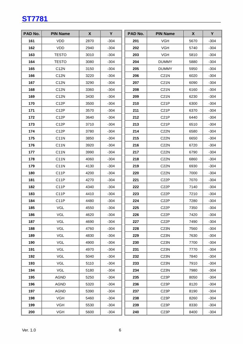
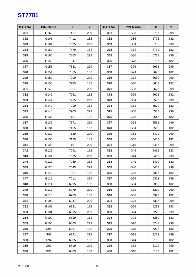
PAD No. PIN Name X Y PAD No. PIN Name X Y
321 G168 7427 299 361 G88 6787 299
322 G166 7411 182 362 G86 6771 182
323 G164 7395 299 363 G84 6755 299
324 G162 7379 182 364 G82 6739 182
325 G160 7363 299 365 G80 6723 299
326 G158 7347 182 366 G78 6707 182
327 G156 7331 299 367 G76 6691 299
328 G154 7315 182 368 G74 6675 182
329 G152 7299 299 369 G72 6659 299
330 G150 7283 182 370 G70 6643 182
331 G148 7267 299 371 G68 6627 299
332 G146 7251 182 372 G66 6611 182
333 G144 7235 299 373 G64 6595 299
334 G142 7219 182 374 G62 6579 182
335 G140 7203 299 375 G60 6563 299
336 G138 7187 182 376 G58 6547 182
337 G136 7171 299 377 G56 6531 299
338 G134 7155 182 378 G54 6515 182
339 G132 7139 299 379 G52 6499 299
340 G130 7123 182 380 G50 6483 182
341 G128 7107 299 381 G48 6467 299
342 G126 7091 182 382 G46 6451 182
343 G124 7075 299 383 G44 6435 299
344 G122 7059 182 384 G42 6419 182
345 G120 7043 299 385 G40 6403 299
346 G118 7027 182 386 G38 6387 182
347 G116 7011 299 387 G36 6371 299
348 G114 6995 182 388 G34 6355 182
349 G112 6979 299 389 G32 6339 299
350 G110 6963 182 390 G30 6323 182
351 G108 6947 299 391 G28 6307 299
352 G106 6931 182 392 G26 6291 182
353 G104 6915 299 393 G24 6275 299
354 G102 6899 182 394 G22 6259 182
355 G100 6883 299 395 G20 6243 299
356 G98 6867 182 396 G18 6227 182
357 G96 6851 299 397 G16 6211 299
358 G94 6835 182 398 G14 6195 182
359 G92 6819 299 399 G12 6179 299
360 G90 6803 182 400 G10 6163 182
ST7781
Ver. 1.0 9
PAD No. PIN Name X Y PAD No. PIN Name X Y
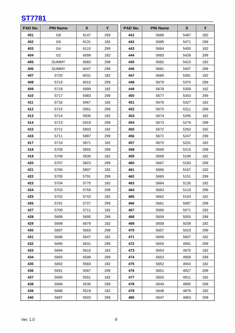
401 G8 6147 299 441 S686 5487 182
402 G6 6131 182 442 S685 5471 299
403 G4 6115 299 443 S684 5455 182
404 G2 6099 182 444 S683 5439 299
405 DUMMY 6083 299 445 S682 5423 182
406 DUMMY 6047 299 446 S681 5407 299
407 S720 6031 182 447 S680 5391 182
408 S719 6015 299 448 S679 5375 299
409 S718 5999 182 449 S678 5359 182
410 S717 5983 299 450 S677 5343 299
411 S716 5967 182 451 S676 5327 182
412 S715 5951 299 452 S675 5311 299
413 S714 5935 182 453 S674 5295 182
414 S713 5919 299 454 S673 5279 299
415 S712 5903 182 455 S672 5263 182
416 S711 5887 299 456 S671 5247 299
417 S710 5871 182 457 S670 5231 182
418 S709 5855 299 458 S669 5215 299
419 S708 5839 182 459 S668 5199 182
420 S707 5823 299 460 S667 5183 299
421 S706 5807 182 461 S666 5167 182
422 S705 5791 299 462 S665 5151 299
423 S704 5775 182 463 S664 5135 182
424 S703 5759 299 464 S663 5119 299
425 S702 5743 182 465 S662 5103 182
426 S701 5727 299 466 S661 5087 299
427 S700 5711 182 467 S660 5071 182
428 S699 5695 299 468 S659 5055 299
429 S698 5679 182 469 S658 5039 182
430 S697 5663 299 470 S657 5023 299
431 S696 5647 182 471 S656 5007 182
432 S695 5631 299 472 S655 4991 299
433 S694 5615 182 473 S654 4975 182
434 S693 5599 299 474 S653 4959 299
435 S692 5583 182 475 S652 4943 182
436 S691 5567 299 476 S651 4927 299
437 S690 5551 182 477 S650 4911 182
438 S689 5535 299 478 S649 4895 299
439 S688 5519 182 479 S648 4879 182
440 S687 5503 299 480 S647 4863 299

ST7781
Ver. 1.0 10
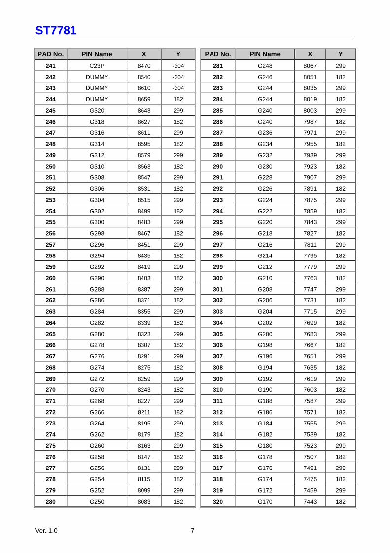
PAD No. PIN Name X Y PAD No. PIN Name X Y
481 S646 4847 182 521 S606 4207 182
482 S645 4831 299 522 S605 4191 299
483 S644 4815 182 523 S604 4175 182
484 S643 4799 299 524 S603 4159 299
485 S642 4783 182 525 S602 4143 182
486 S641 4767 299 526 S601 4127 299
487 S640 4751 182 527 S600 4111 182
488 S639 4735 299 528 S599 4095 299
489 S638 4719 182 529 S598 4079 182
490 S637 4703 299 530 S597 4063 299
491 S636 4687 182 531 S596 4047 182
492 S635 4671 299 532 S595 4031 299
493 S634 4655 182 533 S594 4015 182
494 S633 4639 299 534 S593 3999 299
495 S632 4623 182 535 S592 3983 182
496 S631 4607 299 536 S591 3967 299
497 S630 4591 182 537 S590 3951 182
498 S629 4575 299 538 S589 3935 299
499 S628 4559 182 539 S588 3919 182
500 S627 4543 299 540 S587 3903 299
501 S626 4527 182 541 S586 3887 182
502 S625 4511 299 542 S585 3871 299
503 S624 4495 182 543 S584 3855 182
504 S623 4479 299 544 S583 3839 299
505 S622 4463 182 545 S582 3823 182
506 S621 4447 299 546 S581 3807 299
507 S620 4431 182 547 S580 3791 182
508 S619 4415 299 548 S579 3775 299
509 S618 4399 182 549 S578 3759 182
510 S617 4383 299 550 S577 3743 299
511 S616 4367 182 551 S576 3727 182
512 S615 4351 299 552 S575 3711 299
513 S614 4335 182 553 S574 3695 182
514 S613 4319 299 554 S573 3679 299
515 S612 4303 182 555 S572 3663 182
516 S611 4287 299 556 S571 3647 299
517 S610 4271 182 557 S570 3631 182
518 S609 4255 299 558 S569 3615 299
519 S608 4239 182 559 S568 3599 182
520 S607 4223 299 560 S567 3583 299
ST7781
Ver. 1.0 11
PAD No. PIN Name X Y PAD No. PIN Name X Y
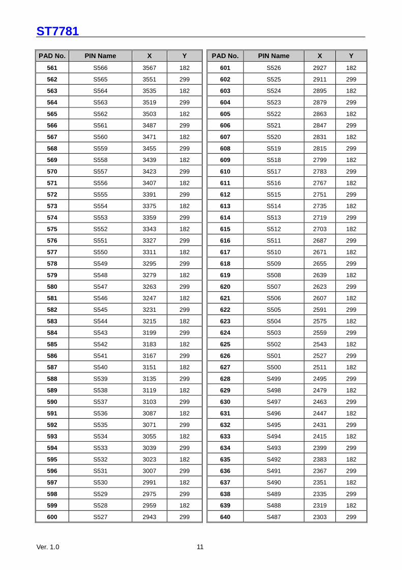
561 S566 3567 182 601 S526 2927 182
562 S565 3551 299 602 S525 2911 299
563 S564 3535 182 603 S524 2895 182
564 S563 3519 299 604 S523 2879 299
565 S562 3503 182 605 S522 2863 182
566 S561 3487 299 606 S521 2847 299
567 S560 3471 182 607 S520 2831 182
568 S559 3455 299 608 S519 2815 299
569 S558 3439 182 609 S518 2799 182
570 S557 3423 299 610 S517 2783 299
571 S556 3407 182 611 S516 2767 182
572 S555 3391 299 612 S515 2751 299
573 S554 3375 182 613 S514 2735 182
574 S553 3359 299 614 S513 2719 299
575 S552 3343 182 615 S512 2703 182
576 S551 3327 299 616 S511 2687 299
577 S550 3311 182 617 S510 2671 182
578 S549 3295 299 618 S509 2655 299
579 S548 3279 182 619 S508 2639 182
580 S547 3263 299 620 S507 2623 299
581 S546 3247 182 621 S506 2607 182
582 S545 3231 299 622 S505 2591 299
583 S544 3215 182 623 S504 2575 182
584 S543 3199 299 624 S503 2559 299
585 S542 3183 182 625 S502 2543 182
586 S541 3167 299 626 S501 2527 299
587 S540 3151 182 627 S500 2511 182
588 S539 3135 299 628 S499 2495 299
589 S538 3119 182 629 S498 2479 182
590 S537 3103 299 630 S497 2463 299
591 S536 3087 182 631 S496 2447 182
592 S535 3071 299 632 S495 2431 299
593 S534 3055 182 633 S494 2415 182
594 S533 3039 299 634 S493 2399 299
595 S532 3023 182 635 S492 2383 182
596 S531 3007 299 636 S491 2367 299
597 S530 2991 182 637 S490 2351 182
598 S529 2975 299 638 S489 2335 299
599 S528 2959 182 639 S488 2319 182
600 S527 2943 299 640 S487 2303 299
ST7781
Ver. 1.0 12
PAD No. PIN Name X Y PAD No. PIN Name X Y
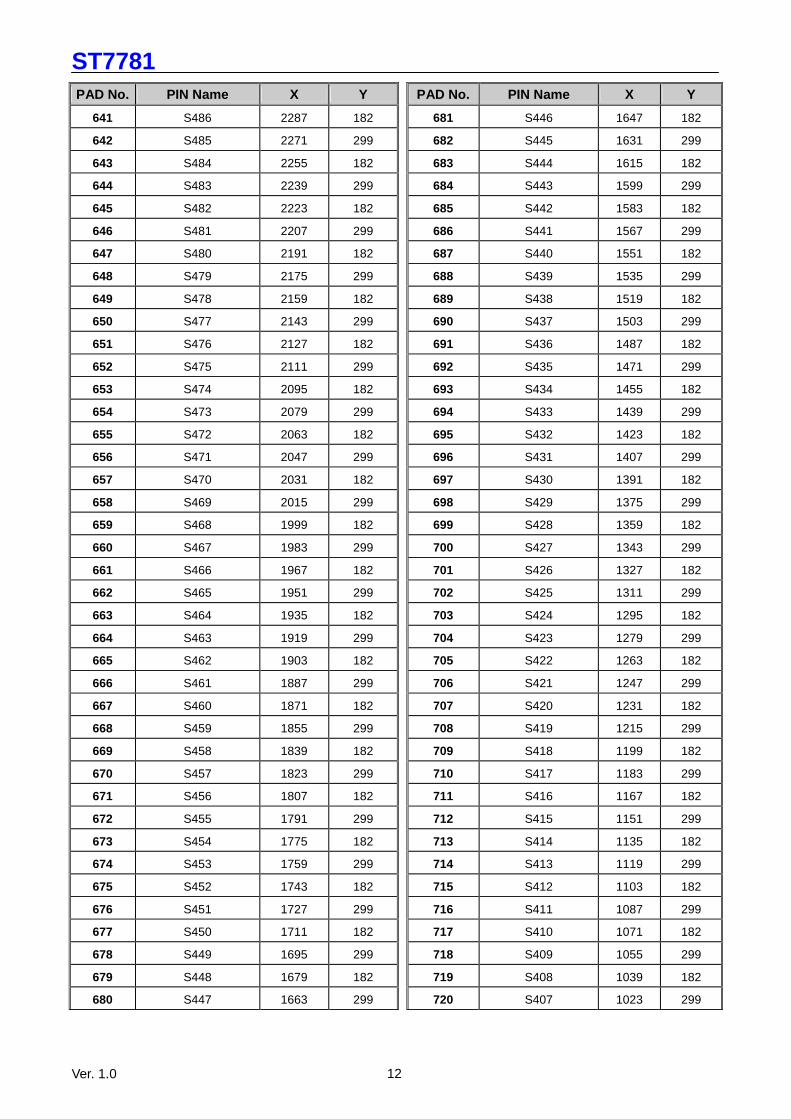
641 S486 2287 182 681 S446 1647 182
642 S485 2271 299 682 S445 1631 299
643 S484 2255 182 683 S444 1615 182
644 S483 2239 299 684 S443 1599 299
645 S482 2223 182 685 S442 1583 182
646 S481 2207 299 686 S441 1567 299
647 S480 2191 182 687 S440 1551 182
648 S479 2175 299 688 S439 1535 299
649 S478 2159 182 689 S438 1519 182
650 S477 2143 299 690 S437 1503 299
651 S476 2127 182 691 S436 1487 182
652 S475 2111 299 692 S435 1471 299
653 S474 2095 182 693 S434 1455 182
654 S473 2079 299 694 S433 1439 299
655 S472 2063 182 695 S432 1423 182
656 S471 2047 299 696 S431 1407 299
657 S470 2031 182 697 S430 1391 182
658 S469 2015 299 698 S429 1375 299
659 S468 1999 182 699 S428 1359 182
660 S467 1983 299 700 S427 1343 299
661 S466 1967 182 701 S426 1327 182
662 S465 1951 299 702 S425 1311 299
663 S464 1935 182 703 S424 1295 182
664 S463 1919 299 704 S423 1279 299
665 S462 1903 182 705 S422 1263 182
666 S461 1887 299 706 S421 1247 299
667 S460 1871 182 707 S420 1231 182
668 S459 1855 299 708 S419 1215 299
669 S458 1839 182 709 S418 1199 182
670 S457 1823 299 710 S417 1183 299
671 S456 1807 182 711 S416 1167 182
672 S455 1791 299 712 S415 1151 299
673 S454 1775 182 713 S414 1135 182
674 S453 1759 299 714 S413 1119 299
675 S452 1743 182 715 S412 1103 182
676 S451 1727 299 716 S411 1087 299
677 S450 1711 182 717 S410 1071 182
678 S449 1695 299 718 S409 1055 299
679 S448 1679 182 719 S408 1039 182
680 S447 1663 299 720 S407 1023 299
ST7781
Ver. 1.0 13
PAD No. PIN Name X Y PAD No. PIN Name X Y
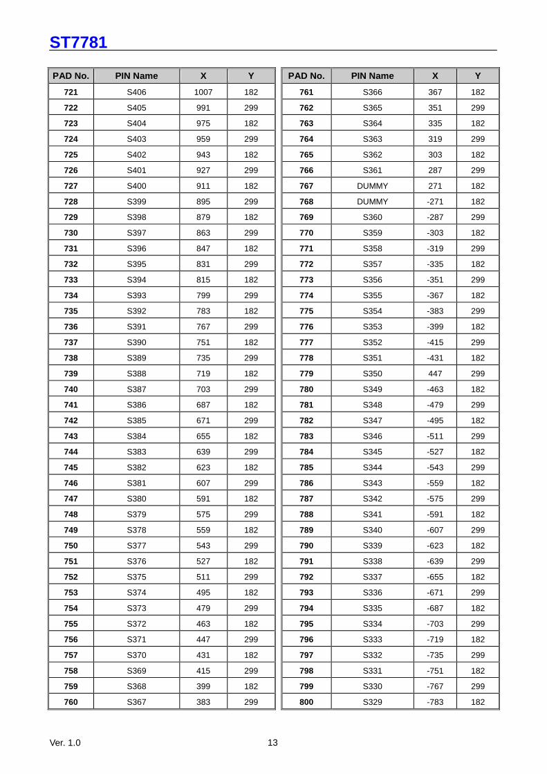
721 S406 1007 182 761 S366 367 182
722 S405 991 299 762 S365 351 299
723 S404 975 182 763 S364 335 182
724 S403 959 299 764 S363 319 299
725 S402 943 182 765 S362 303 182
726 S401 927 299 766 S361 287 299
727 S400 911 182 767 DUMMY 271 182
728 S399 895 299 768 DUMMY -271 182
729 S398 879 182 769 S360 -287 299
730 S397 863 299 770 S359 -303 182
731 S396 847 182 771 S358 -319 299
732 S395 831 299 772 S357 -335 182
733 S394 815 182 773 S356 -351 299
734 S393 799 299 774 S355 -367 182
735 S392 783 182 775 S354 -383 299
736 S391 767 299 776 S353 -399 182
737 S390 751 182 777 S352 -415 299
738 S389 735 299 778 S351 -431 182
739 S388 719 182 779 S350 447 299
740 S387 703 299 780 S349 -463 182
741 S386 687 182 781 S348 -479 299
742 S385 671 299 782 S347 -495 182
743 S384 655 182 783 S346 -511 299
744 S383 639 299 784 S345 -527 182
745 S382 623 182 785 S344 -543 299
746 S381 607 299 786 S343 -559 182
747 S380 591 182 787 S342 -575 299
748 S379 575 299 788 S341 -591 182
749 S378 559 182 789 S340 -607 299
750 S377 543 299 790 S339 -623 182
751 S376 527 182 791 S338 -639 299
752 S375 511 299 792 S337 -655 182
753 S374 495 182 793 S336 -671 299
754 S373 479 299 794 S335 -687 182
755 S372 463 182 795 S334 -703 299
756 S371 447 299 796 S333 -719 182
757 S370 431 182 797 S332 -735 299
758 S369 415 299 798 S331 -751 182
759 S368 399 182 799 S330 -767 299
760 S367 383 299 800 S329 -783 182
ST7781
Ver. 1.0 14
PAD No. PIN Name X Y PAD No. PIN Name X Y
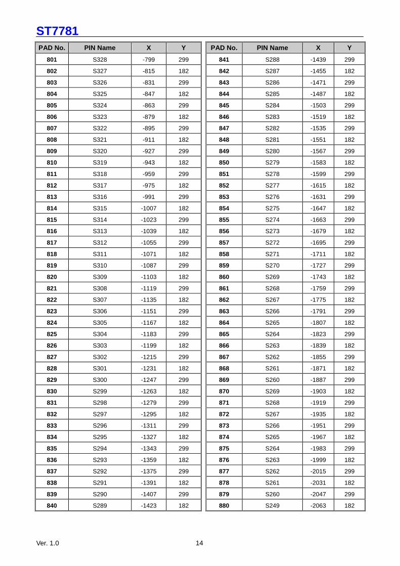
801 S328 -799 299 841 S288 -1439 299
802 S327 -815 182 842 S287 -1455 182
803 S326 -831 299 843 S286 -1471 299
804 S325 -847 182 844 S285 -1487 182
805 S324 -863 299 845 S284 -1503 299
806 S323 -879 182 846 S283 -1519 182
807 S322 -895 299 847 S282 -1535 299
808 S321 -911 182 848 S281 -1551 182
809 S320 -927 299 849 S280 -1567 299
810 S319 -943 182 850 S279 -1583 182
811 S318 -959 299 851 S278 -1599 299
812 S317 -975 182 852 S277 -1615 182
813 S316 -991 299 853 S276 -1631 299
814 S315 -1007 182 854 S275 -1647 182
815 S314 -1023 299 855 S274 -1663 299
816 S313 -1039 182 856 S273 -1679 182
817 S312 -1055 299 857 S272 -1695 299
818 S311 -1071 182 858 S271 -1711 182
819 S310 -1087 299 859 S270 -1727 299
820 S309 -1103 182 860 S269 -1743 182
821 S308 -1119 299 861 S268 -1759 299
822 S307 -1135 182 862 S267 -1775 182
823 S306 -1151 299 863 S266 -1791 299
824 S305 -1167 182 864 S265 -1807 182
825 S304 -1183 299 865 S264 -1823 299
826 S303 -1199 182 866 S263 -1839 182
827 S302 -1215 299 867 S262 -1855 299
828 S301 -1231 182 868 S261 -1871 182
829 S300 -1247 299 869 S260 -1887 299
830 S299 -1263 182 870 S269 -1903 182
831 S298 -1279 299 871 S268 -1919 299
832 S297 -1295 182 872 S267 -1935 182
833 S296 -1311 299 873 S266 -1951 299
834 S295 -1327 182 874 S265 -1967 182
835 S294 -1343 299 875 S264 -1983 299
836 S293 -1359 182 876 S263 -1999 182
837 S292 -1375 299 877 S262 -2015 299
838 S291 -1391 182 878 S261 -2031 182
839 S290 -1407 299 879 S260 -2047 299
840 S289 -1423 182 880 S249 -2063 182

ST7781
Ver. 1.0 15
PAD No. PIN Name X Y PAD No. PIN Name X Y
881 S248 -2079 299 921 S208 -2719 299
882 S247 -2095 182 922 S207 -2735 182
883 S246 -2111 299 923 S206 -2751 299
884 S245 -2127 182 924 S205 -2767 182
885 S244 -2143 299 925 S204 -2783 299
886 S243 -2159 182 926 S203 -2799 182
887 S242 -2175 299 927 S202 -2815 299
888 S241 -2191 182 928 S201 -2831 182
889 S240 -2207 299 929 S200 -2847 299
890 S239 -2223 182 930 S199 -2863 182
891 S238 -2239 299 931 S198 -2879 299
892 S237 -2255 182 932 S197 -2895 182
893 S236 -2271 299 933 S196 -2911 299
894 S235 -2287 182 934 S195 -2927 182
895 S234 -2303 299 935 S194 -2943 299
896 S233 -2319 182 936 S193 -2959 182
897 S232 -2335 299 937 S192 -2975 299
898 S231 -2351 182 938 S191 -2991 182
899 S230 -2367 299 939 S190 -3007 299
900 S229 -2383 182 940 S189 -3023 182
901 S228 -2399 299 941 S188 -3039 299
902 S227 -2415 182 942 S187 -3055 182
903 S226 -2431 299 943 S186 -3071 299
904 S225 -2447 182 944 S185 -3087 182
905 S224 -2463 299 945 S184 -3103 299
906 S223 -2479 182 946 S183 -3119 182
907 S222 -2495 299 947 S182 -3135 299
908 S221 -2511 182 948 S181 -3151 182
909 S220 -2527 299 949 S180 -3167 299
910 S219 -2543 182 950 S179 -3183 182
911 S218 -2559 299 951 S178 -3199 299
912 S217 -2575 182 952 S177 -3215 182
913 S216 -2591 299 953 S176 -3231 299
914 S215 -2607 182 954 S175 -3247 182
915 S214 -2623 299 955 S174 -3263 299
916 S213 -2639 182 956 S173 -3279 182
917 S212 -2655 299 957 S172 -3295 299
918 S211 -2671 182 958 S171 -3311 182
919 S210 -2687 299 959 S170 -3327 299
920 S209 -2703 182 960 S169 -3343 182
ST7781
Ver. 1.0 16
PAD No. PIN Name X Y PAD No. PIN Name X Y
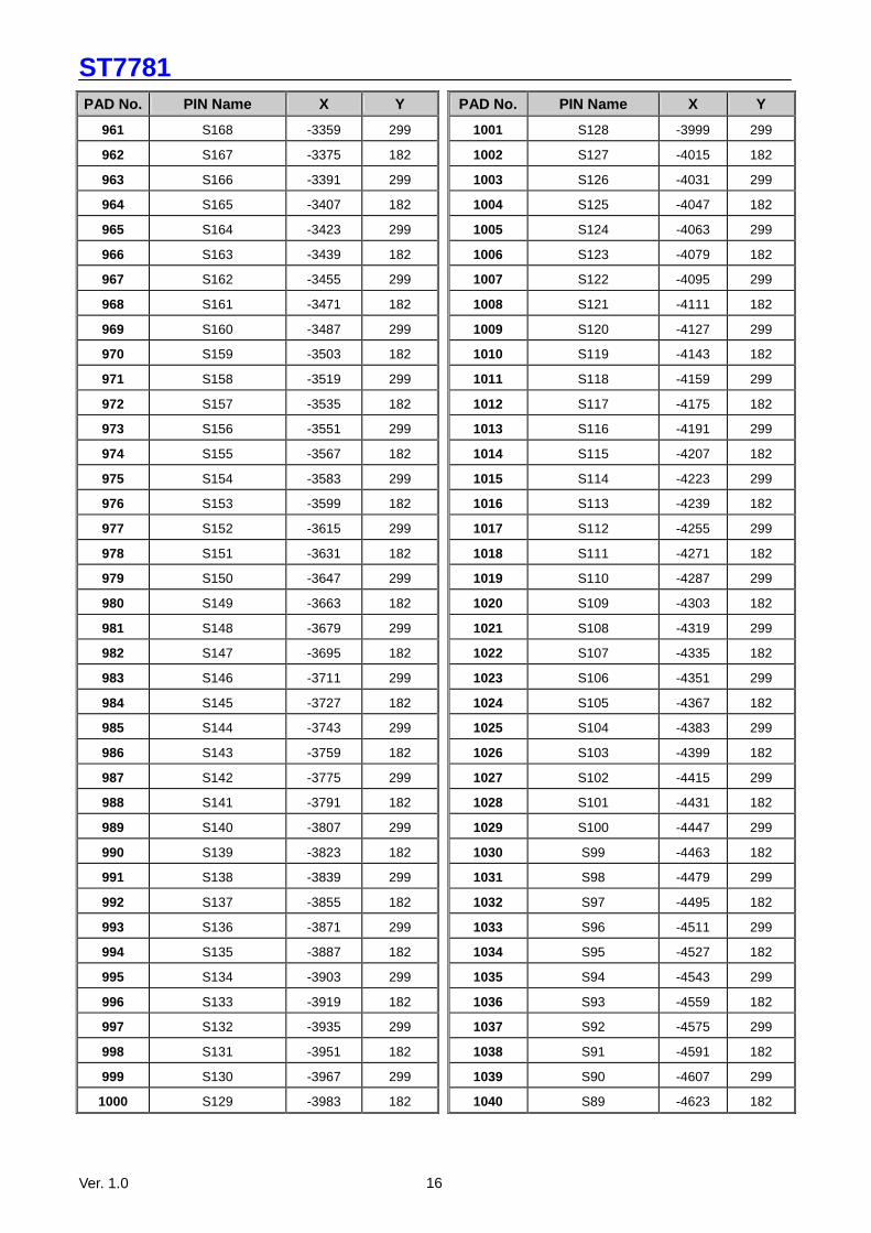
961 S168 -3359 299 1001 S128 -3999 299
962 S167 -3375 182 1002 S127 -4015 182
963 S166 -3391 299 1003 S126 -4031 299
964 S165 -3407 182 1004 S125 -4047 182
965 S164 -3423 299 1005 S124 -4063 299
966 S163 -3439 182 1006 S123 -4079 182
967 S162 -3455 299 1007 S122 -4095 299
968 S161 -3471 182 1008 S121 -4111 182
969 S160 -3487 299 1009 S120 -4127 299
970 S159 -3503 182 1010 S119 -4143 182
971 S158 -3519 299 1011 S118 -4159 299
972 S157 -3535 182 1012 S117 -4175 182
973 S156 -3551 299 1013 S116 -4191 299
974 S155 -3567 182 1014 S115 -4207 182
975 S154 -3583 299 1015 S114 -4223 299
976 S153 -3599 182 1016 S113 -4239 182
977 S152 -3615 299 1017 S112 -4255 299
978 S151 -3631 182 1018 S111 -4271 182
979 S150 -3647 299 1019 S110 -4287 299
980 S149 -3663 182 1020 S109 -4303 182
981 S148 -3679 299 1021 S108 -4319 299
982 S147 -3695 182 1022 S107 -4335 182
983 S146 -3711 299 1023 S106 -4351 299
984 S145 -3727 182 1024 S105 -4367 182
985 S144 -3743 299 1025 S104 -4383 299
986 S143 -3759 182 1026 S103 -4399 182
987 S142 -3775 299 1027 S102 -4415 299
988 S141 -3791 182 1028 S101 -4431 182
989 S140 -3807 299 1029 S100 -4447 299
990 S139 -3823 182 1030 S99 -4463 182
991 S138 -3839 299 1031 S98 -4479 299
992 S137 -3855 182 1032 S97 -4495 182
993 S136 -3871 299 1033 S96 -4511 299
994 S135 -3887 182 1034 S95 -4527 182
995 S134 -3903 299 1035 S94 -4543 299
996 S133 -3919 182 1036 S93 -4559 182
997 S132 -3935 299 1037 S92 -4575 299
998 S131 -3951 182 1038 S91 -4591 182
999 S130 -3967 299 1039 S90 -4607 299
1000 S129 -3983 182 1040 S89 -4623 182

ST7781
Ver. 1.0 17
PAD No. PIN Name X Y PAD No. PIN Name X Y
1041 S88 -4639 299 1081 S48 -5279 299
1042 S87 -4655 182 1082 S47 -5295 182
1043 S86 -4671 299 1083 S46 -5311 299
1044 S85 -4687 182 1084 S45 -5327 182
1045 S84 -4703 299 1085 S44 -5343 299
1046 S83 -4719 182 1086 S43 -5359 182
1047 S82 -4735 299 1087 S42 -5375 299
1048 S81 -4751 182 1088 S41 -5391 182
1049 S80 -4767 299 1089 S40 -5407 299
1050 S79 -4783 182 1090 S39 -5423 182
1051 S78 -4799 299 1091 S38 -5439 299
1052 S77 -4815 182 1092 S37 -5455 182
1053 S76 -4831 299 1093 S36 -5471 299
1054 S75 -4847 182 1094 S35 -5487 182
1055 S74 -4863 299 1095 S34 -5503 299
1056 S73 -4879 182 1096 S33 -5519 182
1057 S72 -4895 299 1097 S32 -5535 299
1058 S71 -4911 182 1098 S31 -5551 182
1059 S70 -4927 299 1099 S30 -5567 299
1060 S69 -4943 182 1100 S29 -5583 182
1061 S68 -4959 299 1101 S28 -5599 299
1062 S67 -4975 182 1102 S27 -5615 182
1063 S66 -4991 299 1103 S26 -5631 299
1064 S65 -5007 182 1104 S25 -5647 182
1065 S64 -5023 299 1105 S24 -5663 299
1066 S63 -5039 182 1106 S23 -5679 182
1067 S62 -5055 299 1107 S22 -5695 299
1068 S61 -5071 182 1108 S21 -5711 182
1069 S60 -5087 299 1109 S20 -5727 299
1070 S59 -5103 182 1110 S19 -5743 182
1071 S58 -5119 299 1111 S18 -5759 299
1072 S57 -5135 182 1112 S17 -5775 182
1073 S56 -5151 299 1113 S16 -5791 299
1074 S55 -5167 182 1114 S15 -5807 182
1075 S54 -5183 299 1115 S14 -5823 299
1076 S53 -5199 182 1116 S13 -5839 182
1077 S52 -5215 299 1117 S12 -5855 299
1078 S51 -5231 182 1118 S11 -5871 182
1079 S50 -5247 299 1119 S10 -5887 299
1080 S49 -5263 182 1120 S9 -5903 182
ST7781
Ver. 1.0 18
PAD No. PIN Name X Y PAD No. PIN Name X Y
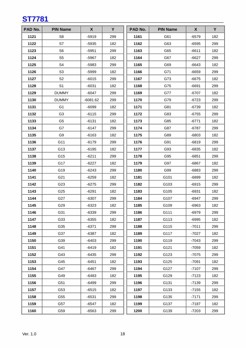
1121 S8 -5919 299 1161 G61 -6579 182
1122 S7 -5935 182 1162 G63 -6595 299
1123 S6 -5951 299 1163 G65 -6611 182
1124 S5 -5967 182 1164 G67 -6627 299
1125 S4 -5983 299 1165 G69 -6643 182
1126 S3 -5999 182 1166 G71 -6659 299
1127 S2 -6015 299 1167 G73 -6675 182
1128 S1 -6031 182 1168 G75 -6691 299
1129 DUMMY -6047 299 1169 G77 -6707 182
1130 DUMMY -6081.62 299 1170 G79 -6723 299
1131 G1 -6099 182 1171 G81 -6739 182
1132 G3 -6115 299 1172 G83 -6755 299
1133 G5 -6131 182 1173 G85 -6771 182
1134 G7 -6147 299 1174 G87 -6787 299
1135 G9 -6163 182 1175 G89 -6803 182
1136 G11 -6179 299 1176 G91 -6819 299
1137 G13 -6195 182 1177 G93 -6835 182
1138 G15 -6211 299 1178 G95 -6851 299
1139 G17 -6227 182 1179 G97 -6867 182
1140 G19 -6243 299 1180 G99 -6883 299
1141 G21 -6259 182 1181 G101 -6899 182
1142 G23 -6275 299 1182 G103 -6915 299
1143 G25 -6291 182 1183 G105 -6931 182
1144 G27 -6307 299 1184 G107 -6947 299
1145 G29 -6323 182 1185 G109 -6963 182
1146 G31 -6339 299 1186 G111 -6979 299
1147 G33 -6355 182 1187 G113 -6995 182
1148 G35 -6371 299 1188 G115 -7011 299
1149 G37 -6387 182 1189 G117 -7027 182
1150 G39 -6403 299 1190 G119 -7043 299
1151 G41 -6419 182 1191 G121 -7059 182
1152 G43 -6435 299 1192 G123 -7075 299
1153 G45 -6451 182 1193 G125 -7091 182
1154 G47 -6467 299 1194 G127 -7107 299
1155 G49 -6483 182 1195 G129 -7123 182
1156 G51 -6499 299 1196 G131 -7139 299
1157 G53 -6515 182 1197 G133 -7155 182
1158 G55 -6531 299 1198 G135 -7171 299
1159 G57 -6547 182 1199 G137 -7187 182
1160 G59 -6563 299 1200 G139 -7203 299
ST7781
Ver. 1.0 19
PAD No. PIN Name X Y PAD No. PIN Name X Y
1201 G141 -7219 182 1241 G221 -7859 182
1202 G143 -7235 299 1242 G223 -7875 299
1203 G145 -7251 182 1243 G225 -7891 182
1204 G147 -7267 299 1244 G227 -7907 299
1205 G149 -7283 182 1245 G229 -7923 182
1206 G151 -7299 299 1246 G231 -7939 299
1207 G153 -7315 182 1247 G233 -7955 182
1208 G155 -7331 299 1248 G235 -7971 299
1209 G157 -7347 182 1249 G237 -7987 182
1210 G159 -7363 299 1250 G239 -8003 299
1211 G161 -7379 182 1251 G241 -8019 182
1212 G163 -7395 299 1252 G243 -8035 299
1213 G165 -7411 182 1253 G245 -8051 182
1214 G167 -7427 299 1254 G247 -8067 299
1215 G169 -7443 182 1255 G249 -8083 182
1216 G171 -7459 299 1256 G251 -8099 299
1217 G173 -7475 182 1257 G253 -8115 182
1218 G175 -7491 299 1258 G255 -8131 299
1219 G177 -7507 182 1259 G257 -8147 182
1220 G179 -7523 299 1260 G259 -8163 299
1221 G181 -7539 182 1261 G261 -8179 182
1222 G183 -7555 299 1262 G263 -8195 299
1223 G185 -7571 182 1263 G265 -8211 182
1224 G187 -7587 299 1264 G267 -8227 299
1225 G189 -7603 182 1265 G269 -8243 182
1226 G191 -7619 299 1266 G271 -8259 299
1227 G193 -7635 182 1267 G273 -8275 182
1228 G195 -7651 299 1268 G275 -8291 299
1229 G197 -7667 182 1269 G277 -8307 182
1230 G199 -7683 299 1270 G279 -8323 299
1231 G201 -7699 182 1271 G281 -8339 182
1232 G203 -7715 299 1272 G283 -8355 299
1233 G205 -7731 182 1273 G285 -8371 182
1234 G207 -7747 299 1274 G287 -8387 299
1235 G209 -7763 182 1275 G289 -8403 182
1236 G211 -7779 299 1276 G291 -8419 299
1237 G213 -7795 182 1277 G293 -8435 182
1238 G215 -7811 299 1278 G295 -8451 299
1239 G217 -7827 182 1279 G297 -8467 182
1240 G219 -7843 299 1280 G299 -8483 299
ST7781
Ver. 1.0 20
PAD No. PIN Name X Y
1281 G301 -8499 182
1282 G303 -8515 299
1283 G305 -8531 182
1284 G307 -8547 299
1285 G309 -8563 182
1286 G311 -8579 299
1287 G313 -8595 182
1288 G315 -8611 299
1289 G317 -8627 182
1290 G319 -8643 299
1291 DUMMY -8659 182
ST7781
Ver. 1.0 21
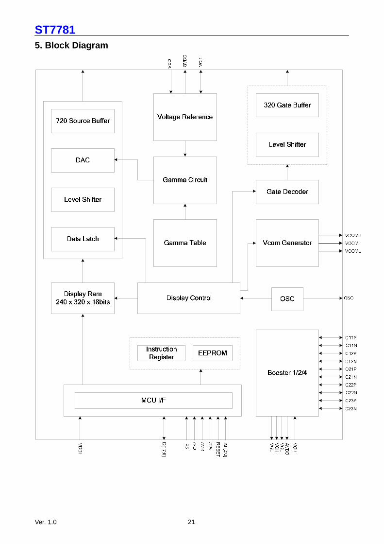
5. Block Diagram
ST7781
Ver. 1.0 22
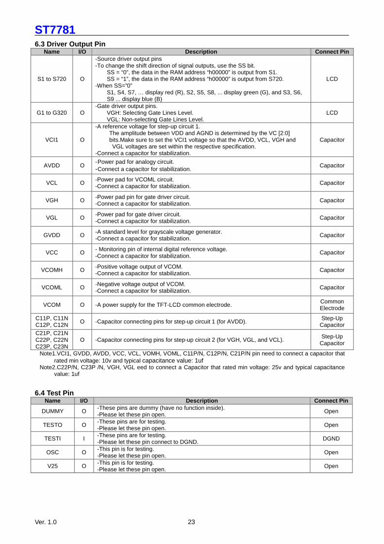
6. Pin Description 6.1 Power Supply Pin
Name I/O Description Connect Pin VDD I Power supply for analog, digital system and booster circuit VDD VDDI I Power supply for I/O system VDDI AGND I System ground for analog system and booster circuit. GND DGND I System ground for I/O system and internal digital system. GND
6.2 Interface Logic Pin
Name I/O Description Connect Pin
IM0~IM3 I
-Select the MCU system interface mode IM3 IM2 IM1 IM0 MCU-Interface Mode DB Pin Use
0 0 1 0 I80-system 16-bit interface DB[17:10] DB[8:1]
0 0 1 1 I80-system 8-bit interface DB[17:10] 1 0 1 0 I80-system 18-bit interface DB[17:0] 1 0 1 1 I80-system 9-bit interface DB[17:9]
DGND/VDDI
RESET I -This signal will reset the driver and it must be applied to properly initialize the chip. MCU
/CS I -Chip select input pin and signal is active low. -This pin can be permanently fixed “Low” in MCU interface mode only. MCU
RS I
-Display data or command selection pin in MCU interface. RS =’1’: display data or parameter. RS =’0’: command.
-If not used, please connect this pin to VDDI or DGND.
MCU
/RD I -Read enable in 8080 MCU parallel interface. MCU /WR I -Write operation enable pin in 8080 MCU parallel interface. MCU
DB[17:0] I/O
-An 18-bit paralled bi-directional data bus for MCU system interface mode 8-bit Interface: DB[17:10] is used 9-bit Interface: DB[17:9] is used
16-bit Interface: DB[17:10] and DB[8:1] is used 18-bit Interface: DB[17:0] is used -If not used, please connect this pin to VDDI or DGND.
MCU
SW_EE I -To use extended command set, please connect this pin to VDDI. -During normal operation, please let this pin open. DGND/VDDI
FMARK O -Output a frame head pulse signal is used as synchronies MCU to frame rate -If not used, Let this pin open -
Note1. When /CS=”1”, there is no influence to the parallel interface. Note2. “1” = VDDI level, “0” = DGND level.
ST7781
Ver. 1.0 23
6.3 Driver Output Pin Name I/O Description Connect Pin
S1 to S720 O
-Source driver output pins -To change the shift direction of signal outputs, use the SS bit.
SS = “0”, the data in the RAM address “h00000” is output from S1. SS = “1”, the data in the RAM address “h00000” is output from S720.
-When SS=”0” S1, S4, S7, … display red (R), S2, S5, S8, ... display green (G), and S3, S6, S9 ... display blue (B)
LCD
G1 to G320 O -Gate driver output pins.
VGH: Selecting Gate Lines Level. VGL: Non-selecting Gate Lines Level.
LCD
VCI1 O
-A reference voltage for step-up circuit 1. The amplitude between VDD and AGND is determined by the VC [2:0] bits.Make sure to set the VCI1 voltage so that the AVDD, VCL, VGH and VGL voltages are set within the respective specification.
-Connect a capacitor for stabilization.
Capacitor
AVDD O - Power pad for analogy circuit. - Connect a capacitor for stabilization. Capacitor
VCL O -Power pad for VCOML circuit. -Connect a capacitor for stabilization. Capacitor
VGH O -Power pad pin for gate driver circuit. -Connect a capacitor for stabilization. Capacitor
VGL O -Power pad for gate driver circuit. -Connect a capacitor for stabilization.
Capacitor
GVDD O -A standard level for grayscale voltage generator. -Connect a capacitor for stabilization. Capacitor
VCC O - Monitoring pin of internal digital reference voltage. -Connect a capacitor for stabilization.
Capacitor
VCOMH O -Positive voltage output of VCOM. -Connect a capacitor for stabilization. Capacitor
VCOML O -Negative voltage output of VCOM. -Connect a capacitor for stabilization. Capacitor
VCOM O -A power supply for the TFT-LCD common electrode. Common Electrode
C11P, C11N C12P, C12N O -Capacitor connecting pins for step-up circuit 1 (for AVDD). Step-Up
Capacitor C21P, C21N C22P, C22N C23P, C23N
O -Capacitor connecting pins for step-up circuit 2 (for VGH, VGL, and VCL). Step-Up Capacitor
Note1.VCI1, GVDD, AVDD, VCC, VCL, VOMH, VOML, C11P/N, C12P/N, C21P/N pin need to connect a capacitor that rated min voltage: 10v and typical capacitance value: 1uf
Note2.C22P/N, C23P /N, VGH, VGL eed to connect a Capacitor that rated min voltage: 25v and typical capacitance value: 1uf
6.4 Test Pin
Name I/O Description Connect Pin
DUMMY O -These pins are dummy (have no function inside). -Please let these pin open. Open
TESTO O -These pins are for testing. -Please let these pin open. Open
TESTI I -These pins are for testing. -Please let these pin connect to DGND. DGND
OSC O -This pin is for testing. -Please let these pin open. Open
V25 O -This pin is for testing. -Please let these pin open. Open
ST7781
Ver. 1.0 24
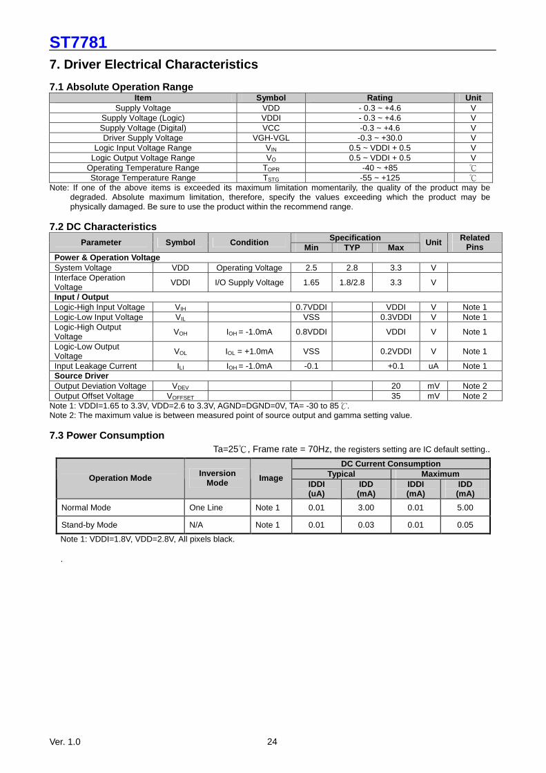
7. Driver Electrical Characteristics 7.1 Absolute Operation Range
Item Symbol Rating Unit Supply Voltage VDD - 0.3 ~ +4.6 V
Supply Voltage (Logic) VDDI - 0.3 ~ +4.6 V Supply Voltage (Digital) VCC -0.3 ~ +4.6 V Driver Supply Voltage VGH-VGL -0.3 ~ +30.0 V
Logic Input Voltage Range VIN 0.5 ~ VDDI + 0.5 V Logic Output Voltage Range VO 0.5 ~ VDDI + 0.5 V
Operating Temperature Range TOPR -40 ~ +85 ℃ Storage Temperature Range TSTG -55 ~ +125 ℃
Note: If one of the above items is exceeded its maximum limitation momentarily, the quality of the product may be degraded. Absolute maximum limitation, therefore, specify the values exceeding which the product may be physically damaged. Be sure to use the product within the recommend range.
7.2 DC Characteristics
Specification Parameter Symbol Condition Min TYP Max
Unit Related Pins
Power & Operation Voltage System Voltage VDD Operating Voltage 2.5 2.8 3.3 V Interface Operation Voltage VDDI I/O Supply Voltage 1.65 1.8/2.8 3.3 V
Input / Output Logic-High Input Voltage VIH 0.7VDDI VDDI V Note 1 Logic-Low Input Voltage VIL VSS 0.3VDDI V Note 1 Logic-High Output Voltage VOH IOH = -1.0mA 0.8VDDI VDDI V Note 1
Logic-Low Output Voltage VOL IOL = +1.0mA VSS 0.2VDDI V Note 1
Input Leakage Current ILI IOH = -1.0mA -0.1 +0.1 uA Note 1 Source Driver Output Deviation Voltage VDEV 20 mV Note 2 Output Offset Voltage VOFFSET 35 mV Note 2
Note 1: VDDI=1.65 to 3.3V, VDD=2.6 to 3.3V, AGND=DGND=0V, TA= -30 to 85℃. Note 2: The maximum value is between measured point of source output and gamma setting value. 7.3 Power Consumption
Ta=25℃, Frame rate = 70Hz, the registers setting are IC default setting..
DC Current Consumption Typical Maximum Operation Mode Inversion
Mode Image IDDI (uA)
IDD (mA)
IDDI (mA)
IDD (mA)
Normal Mode One Line Note 1 0.01 3.00 0.01 5.00
Stand-by Mode N/A Note 1 0.01 0.03 0.01 0.05
Note 1: VDDI=1.8V, VDD=2.8V, All pixels black.
.
ST7781
Ver. 1.0 25
8. System Interface 8.1 Interface Specifications ST7781 has the system interface to read/write the control registers and display memory (DRAM) displaying a moving picture. User can select an optimum interface to display the moving or still picture with efficient data transfer. All display data are stored in the DRAM to reduce the data transfer efforts and only the updating data is necessary to be transferred. User can only update a sub-range of DRAM by using the window address function. ST7781 adopts 18-bit bus interface architecture for high-performance microprocessor. All the functional blocks of ST7781 starts to work after receiving the correct instruction from the external microprocessor by the 18bits, 16bits, 9bits,8bits. The index register (IR) stores the register address to which the instructions and display data will be written. The data/command selection signal (RS), the read/write signals (/RD//WR) and data bus DB[17:0] are used to read/write the instructions and data of ST7781. The registers of the ST7781 are categorized into the following groups. 1. Specify the Index of Register (IR) 2. Read a Status 3. Display Control 4. Power Management Control 5. Display Data Processing 6. Set Internal DRAM Address (AC) 7. Transfer Data to/from the Internal DRAM (R22h) 8. Internal Grayscale γ-Correction (R30h ~ R3Dh) Normally, the display data (DRAM) is most often updated, and in order since the ST7781 can update internal DRAM address automatically as it writes data to the internal DRAM and minimize data transfer by using the window address function, there are fewer loads on the program in the microprocessor.
ST7781
Ver. 1.0 26
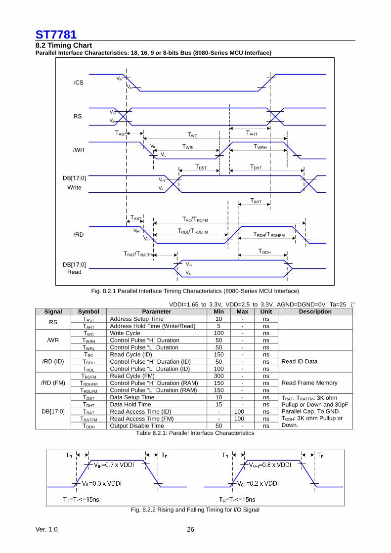
8.2 Timing Chart Parallel Interface Characteristics: 18, 16, 9 or 8-b its Bus (8080-Series MCU Interface)
/CS
RS
/WR
DB[17:0]
Write
/RD
Read
VIH
VIL
VIH
VIL
VIH
VIL
VIH
VIL
VIH
VIL
VIH
VIL
TAST TAHTTWC
TWRL TWRH
TDST TDHT
TAHT
TRC/TRCFM
TRDL/TRDLFM
TAST
TRDH/TRDHFM
TRAT/TRATFMTODH
DB[17:0]
Fig. 8.2.1 Parallel Interface Timing Characteristics (8080-Series MCU Interface)
VDDI=1.65 to 3.3V, VDD=2.5 to 3.3V, AGND=DGND=0V, Ta=25 ℃
Signal Symbol Parameter Min Max Unit Description TAST Address Setup Time 10 - ns RS TAHT Address Hold Time (Write/Read) 5 - ns
TWC Write Cycle 100 - ns TWRH Control Pulse “H” Duration 50 - ns /WR TWRL Control Pulse “L” Duration 50 - ns
TRC Read Cycle (ID) 150 - ns TRDH Control Pulse “H” Duration (ID) 50 - ns /RD (ID) TRDL Control Pulse “L” Duration (ID) 100 - ns
Read ID Data
TRCFM Read Cycle (FM) 300 - ns TRDHFM Control Pulse “H” Duration (RAM) 150 - ns /RD (FM) TRDLFM Control Pulse “L” Duration (RAM) 150 - ns
Read Frame Memory
TDST Data Setup Time 10 - ns TDHT Data Hold Time 15 - ns TRAT Read Access Time (ID) - 100 ns
TRATFM Read Access Time (FM) - 100 ns DB[17:0]
TODH Output Disable Time 50 - ns
TRAT, TRATFM: 3K ohm Pullup or Down and 30pF Parallel Cap. To GND. TODH: 3K ohm Pullup or Down.
Table 8.2.1: Parallel Interface Characteristics
Fig. 8.2.2 Rising and Falling Timing for I/O Signal

ST7781
Ver. 1.0 27
Fig. 8.2.3 Write-to-Read and Read-to-Write Timing
Note: The rising time and falling time (Tr, Tf) of input signal and fall time are specified at 15 ns or less. Logic high and low
levels are specified as 30% and 70% of VDDI for Input signals.
ST7781
Ver. 1.0 28
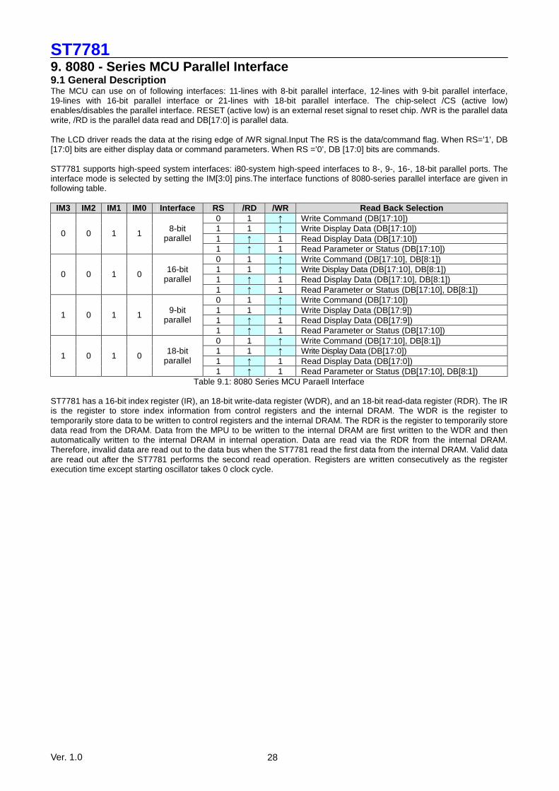
9. 8080 - Series MCU Parallel Interface 9.1 General Description The MCU can use on of following interfaces: 11-lines with 8-bit parallel interface, 12-lines with 9-bit parallel interface, 19-lines with 16-bit parallel interface or 21-lines with 18-bit parallel interface. The chip-select /CS (active low) enables/disables the parallel interface. RESET (active low) is an external reset signal to reset chip. /WR is the parallel data write, /RD is the parallel data read and DB[17:0] is parallel data. The LCD driver reads the data at the rising edge of /WR signal.Input The RS is the data/command flag. When RS=’1’, DB [17:0] bits are either display data or command parameters. When RS =’0’, DB [17:0] bits are commands. ST7781 supports high-speed system interfaces: i80-system high-speed interfaces to 8-, 9-, 16-, 18-bit parallel ports. The interface mode is selected by setting the IM[3:0] pins.The interface functions of 8080-series parallel interface are given in following table.
IM3 IM2 IM1 IM0 Interface RS /RD /WR Read Back Selection 0 1 ↑ Write Command (DB[17:10]) 1 1 ↑ Write Display Data (DB[17:10]) 1 ↑ 1 Read Display Data (DB[17:10])
0 0 1 1 8-bit parallel
1 ↑ 1 Read Parameter or Status (DB[17:10]) 0 1 ↑ Write Command (DB[17:10], DB[8:1]) 1 1 ↑ Write Display Data (DB[17:10], DB[8:1]) 1 ↑ 1 Read Display Data (DB[17:10], DB[8:1])
0 0 1 0 16-bit parallel
1 ↑ 1 Read Parameter or Status (DB[17:10], DB[8:1]) 0 1 ↑ Write Command (DB[17:10]) 1 1 ↑ Write Display Data (DB[17:9]) 1 ↑ 1 Read Display Data (DB[17:9])
1 0 1 1 9-bit parallel
1 ↑ 1 Read Parameter or Status (DB[17:10]) 0 1 ↑ Write Command (DB[17:10], DB[8:1]) 1 1 ↑ Write Display Data (DB[17:0]) 1 ↑ 1 Read Display Data (DB[17:0])
1 0 1 0 18-bit parallel
1 ↑ 1 Read Parameter or Status (DB[17:10], DB[8:1]) Table 9.1: 8080 Series MCU Paraell Interface
ST7781 has a 16-bit index register (IR), an 18-bit write-data register (WDR), and an 18-bit read-data register (RDR). The IR is the register to store index information from control registers and the internal DRAM. The WDR is the register to temporarily store data to be written to control registers and the internal DRAM. The RDR is the register to temporarily store data read from the DRAM. Data from the MPU to be written to the internal DRAM are first written to the WDR and then automatically written to the internal DRAM in internal operation. Data are read via the RDR from the internal DRAM. Therefore, invalid data are read out to the data bus when the ST7781 read the first data from the internal DRAM. Valid data are read out after the ST7781 performs the second read operation. Registers are written consecutively as the register execution time except starting oscillator takes 0 clock cycle.
ST7781
Ver. 1.0 29
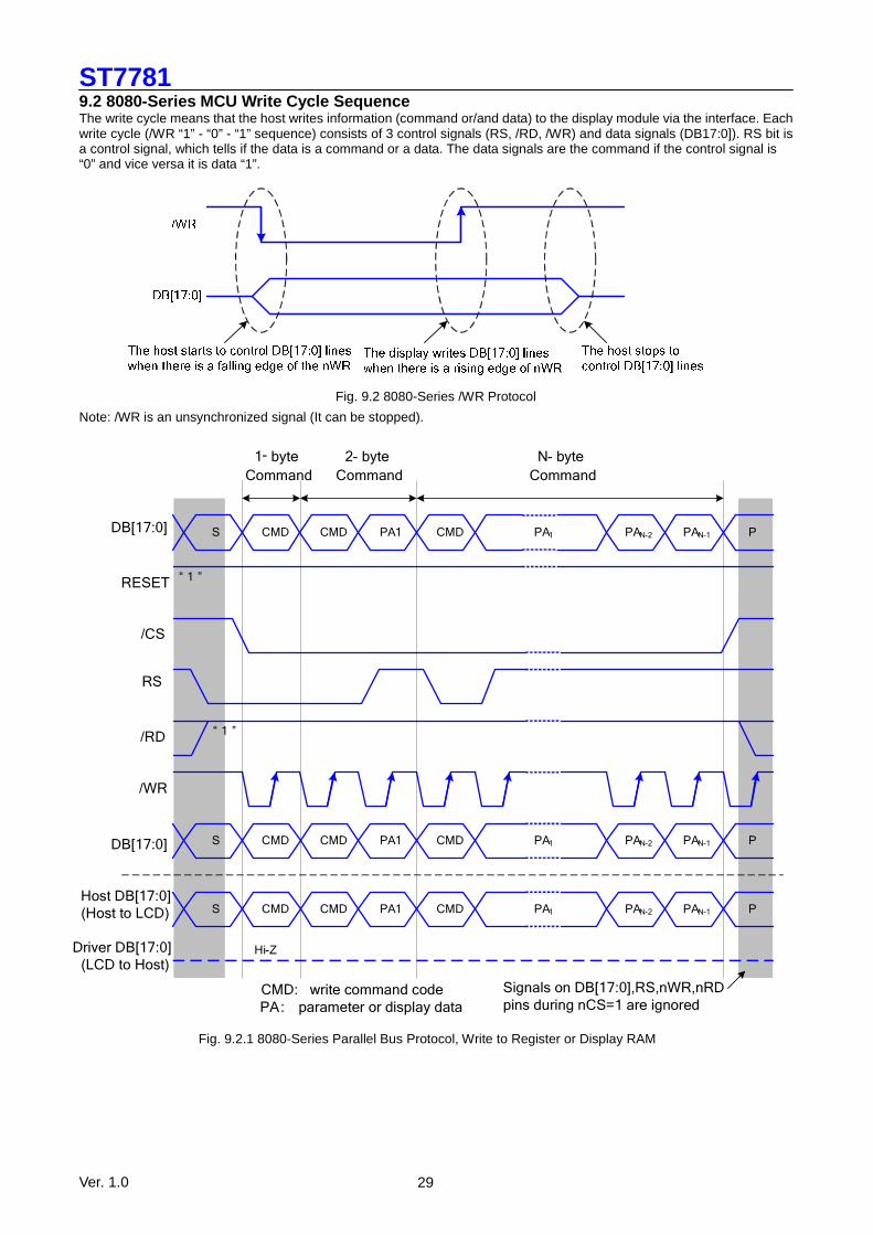
9.2 8080-Series MCU Write Cycle Sequence The write cycle means that the host writes information (command or/and data) to the display module via the interface. Each write cycle (/WR “1” - “0” - “1” sequence) consists of 3 control signals (RS, /RD, /WR) and data signals (DB17:0]). RS bit is a control signal, which tells if the data is a command or a data. The data signals are the command if the control signal is “0” and vice versa it is data “1”.
Fig. 9.2 8080-Series /WR Protocol
Note: /WR is an unsynchronized signal (It can be stopped).
CMD CMD PA1 CMD PA1 PAN-2 PAN-1S P
CMD CMD PA1 CMD PA1 PAN-2 PAN-1S P
CMD CMD PA1 CMD PA1 PAN-2 PAN-1S P
DB[17:0]
RESET
/CS
RS
/RD
/WR
Host DB[17:0](Host to LCD)
Driver DB[17:0](LCD to Host)
“ 1 ”
“ 1 ”
Hi-Z
1- byte
Command
2- byte
Command
N- byte
Command
CMD: write command code
PA: parameter or display data
Signals on DB[17:0],RS,nWR,nRD
pins during nCS=1 are ignored
DB[17:0]
Fig. 9.2.1 8080-Series Parallel Bus Protocol, Write to Register or Display RAM
ST7781
Ver. 1.0 30
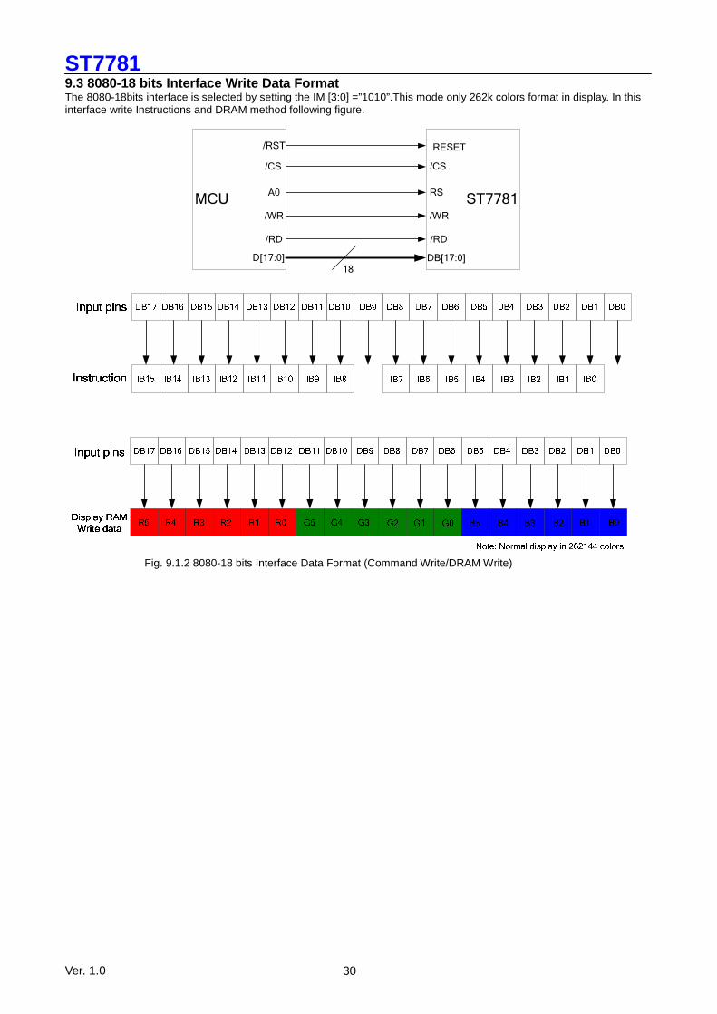
9.3 8080-18 bits Interface Write Data Format The 8080-18bits interface is selected by setting the IM [3:0] =”1010”.This mode only 262k colors format in display. In this interface write Instructions and DRAM method following figure.
MCU ST7781
/CS
A0
/WR
/RD
/RST
D[17:0]
/CS
RS
/WR
/RD
RESET
DB[17:0]18
Fig. 9.1.2 8080-18 bits Interface Data Format (Command Write/DRAM Write)
ST7781
Ver. 1.0 31
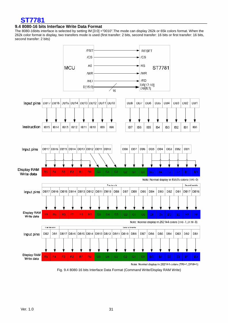
9.4 8080-16 bits Interface Write Data Format The 8080-16bits interface is selected by setting IM [3:0] =”0010”.The mode can display 262k or 65k colors format. When the 262k color format is display, two transfers mode is used (first transfer: 2 bits, second transfer: 16 bits or first transfer: 16 bits, second transfer: 2 bits)
Fig. 9.4 8080-16 bits Interface Data Format (Command Write/Display RAM Write)
ST7781
Ver. 1.0 32
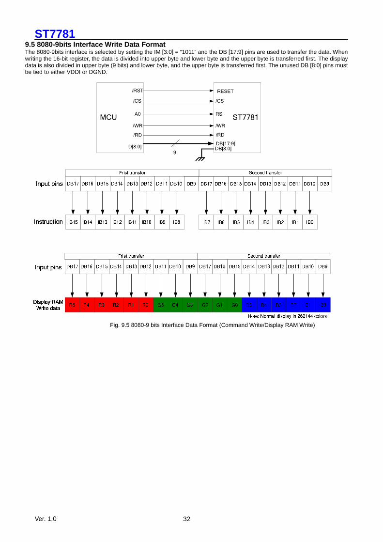
9.5 8080-9bits Interface Write Data Format The 8080-9bits interface is selected by setting the IM [3:0] = “1011” and the DB [17:9] pins are used to transfer the data. When writing the 16-bit register, the data is divided into upper byte and lower byte and the upper byte is transferred first. The display data is also divided in upper byte (9 bits) and lower byte, and the upper byte is transferred first. The unused DB [8:0] pins must be tied to either VDDI or DGND.
MCU ST7781
/CS
A0
/WR
/RD
/RST
D[8:0]
/CS
RS
/WR
/RD
RESET
DB[17:9]
9DB[8:0]
Fig. 9.5 8080-9 bits Interface Data Format (Command Write/Display RAM Write)

ST7781
Ver. 1.0 33
9.6 8080-8bits Interface Write Data Format The 8080 8-bit interface is selected by setting the IM [3:0] as “0011” and the DB [17:10] pins are used to transfer the data. The mode can display 262k or 65k colors format. When writing the 16-bit register, the data is divided into upper byte lower byte and the upper byte is transferred first. The display data is also divided in upper byte (8 bits) and lower byte, and the upper byte is transferred first. The written data is expanded into 18 bits internally (see the figure below) and then written into DRAM. The unused DB [9:0] pins must be tied to either VDDI or DGND.
Fig. 9.6 8080-8 bits interface data format (command write/Display RAM write)
ST7781
Ver. 1.0 34
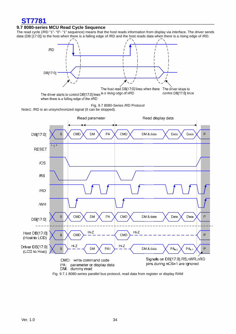
9.7 8080-series MCU Read Cycle Sequence The read cycle (/RD “1”- “0”- “1” sequence) means that the host reads information from display via interface. The driver sends data (DB [17:0]) to the host when there is a falling edge of /RD and the host reads data when there is a rising edge of /RD.
Fig. 9.7 8080-Series /RD Protocol
Note1: /RD is an unsynchronized signal (It can be stopped).
Fig. 9.7.1 8080-series parallel bus protocol, read data from register or display RAM
ST7781
Ver. 1.0 35
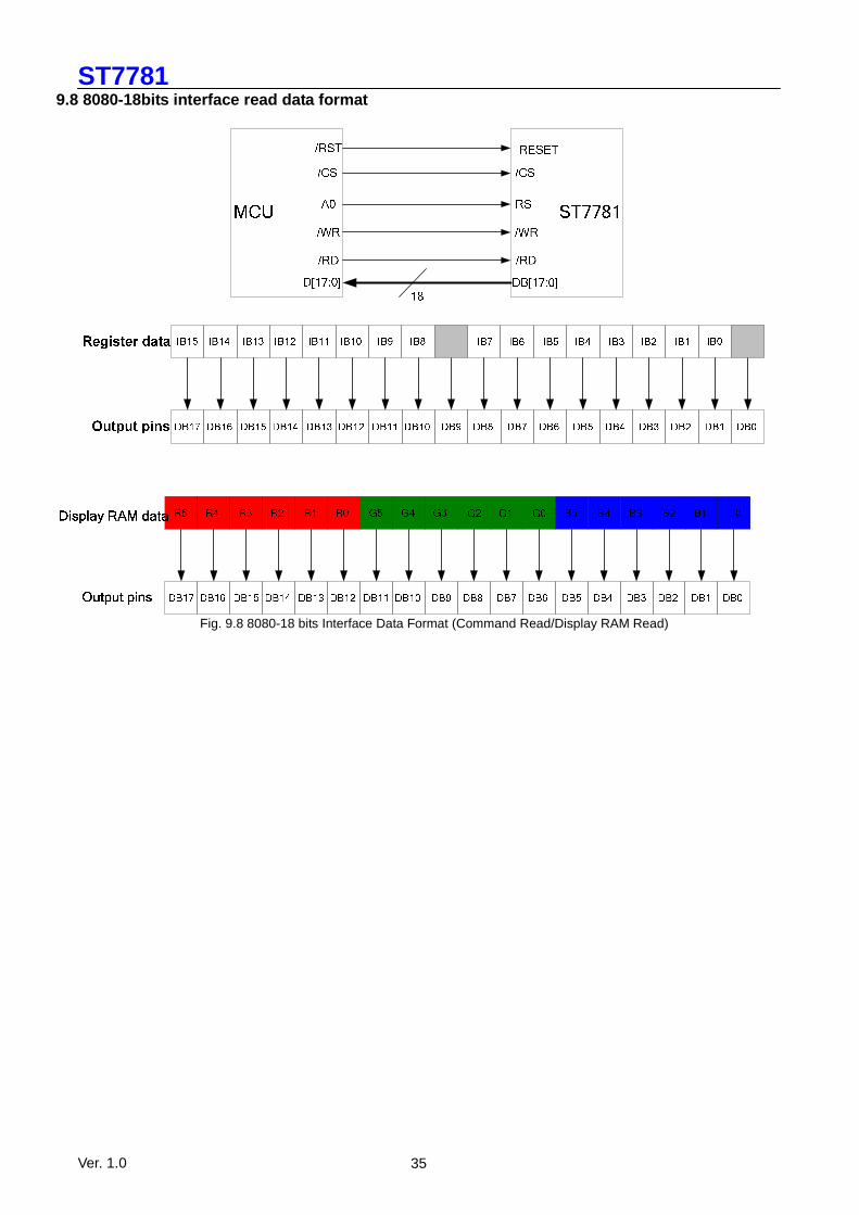
9.8 8080-18bits interface read data format
Fig. 9.8 8080-18 bits Interface Data Format (Command Read/Display RAM Read)
ST7781
Ver. 1.0 36
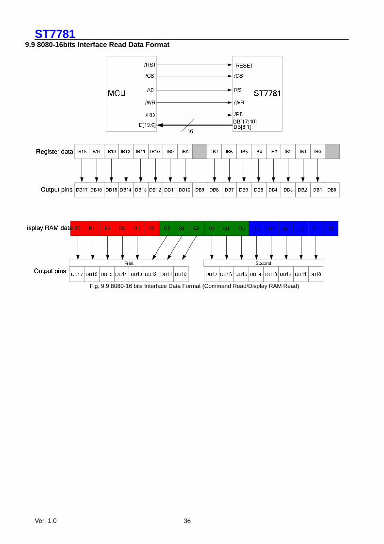
9.9 8080-16bits Interface Read Data Format
Fig. 9.9 8080-16 bits Interface Data Format (Command Read/Display RAM Read)
ST7781
Ver. 1.0 37
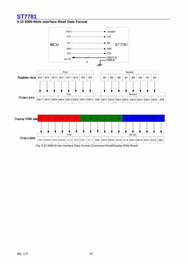
9.10 8080-9bits Interface Read Data Format
Fig. 9.10 8080-9 bits Interface Data Format (Command Read/Display RAM Read)
ST7781
Ver. 1.0 38
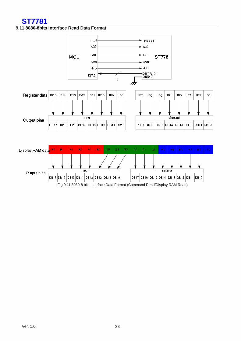
9.11 8080-8bits Interface Read Data Format
Fig.9.11 8080-8 bits Interface Data Format (Command Read/Display RAM Read)
ST7781
Ver. 1.0 39
10. Register Descriptions ST7781 adopts 18-bit bus interface architecture for high-performance microprocessor. All the functional Blocks of ST7781 starts to work after receiving the correct instruction from the external microprocessor by the 18-, 16-, 9-, 8-bit interface. The index register (IR) stores the register address to which the instructions and Display data will be written. The register selection signal (RS), the read/write signals (/RD//WR) and data bus DB[17:0] are used to read/write the instructions and data of ST7781. The registers of the ST7781 are categorized into the following groups. 1. Specify the index of register (IR) 2. Read a status 3. Display control 4. Power management Control 5. Graphics data processing 6. Set internal DRAM address (AC) 7. Transfer data to/from the internal DRAM (R22) 8. Internal grayscale γ-correction (R30 ~ R3D) Normally, the display data (DRAM) is most often updated, and in order since the ST7781 can update internal DRAM address automatically as it writes data to the internal DRAM and minimize data transfer by using the window address function, there are fewer loads on the program in the microprocessor. The way of assigning data to the 16 register bits ( DB [15:0]) varies for each interface. Send registers in accordance with the following data transfer format.
ST7781
Ver. 1.0 40
10.1 Instruction Description No Registers W/R RS D15 D14 D13 D12 D11 D10 D9 D8 D7 D6 D5 D4 D3 D2 D1 D0 IR Index Register W 0 - - - - - - - - ID7 ID6 ID5 ID4 ID3 ID2 ID1 ID0
00h Driver ID Code Read R 1 0 1 1 1 0 1 1 1 1 0 0 0 0 0 1 1 01h Driver Output Control W 1 0 0 0 0 0 SM 0 SS 0 0 0 0 0 0 0 0 02h LCD Driving Wave Control W 1 0 0 0 0 0 1 BC0 EOR 0 0 0 0 0 0 0 0 03h Entry Mode W 1 TRI DFM 0 BGR 0 0 HWM 0 0 0 I/D1 I/D0 AM 0 0 0 04h Resize Control W 1 0 0 0 0 0 0 RCV1 RCV0 0 0 RCH1 RCH0 0 0 RSZ1 RSZ0 07h Display Control 1 W 1 0 0 PTDE1 PTDE0 0 0 BASEE 0 0 GON DTE CL 0 D1 D0 08h Display control 2 W 1 0 FP6 FP5 FP4 FP3 FP2 FP1 FP0 0 BP6 BP5 BP4 BP3 BP2 BP1 BP0 09h Display Control 3 W 1 0 0 0 0 0 PTS2 PTS1 PTS0 0 0 PTG1 PTG0 ISC3 ISC2 ISC1 ISC0 0Ah Display Control 4 W 1 0 0 0 0 0 0 0 0 0 0 0 0 FMARKOE FMI2 FMI1 FMI0 0Dh Frame Marker Position W 1 0 0 0 0 0 0 0 FMP8 FMP7 FMP6 FMP5 FMP4 FMP3 FMP2 FMP1 FMP0 10h Power Control 1 W 1 0 0 0 SAP 0 BT2 BT1 BT0 APE AP2 AP1 AP0 0 0 STB 0 11h Power Control 2 W 1 0 0 0 0 0 DC12 DC11 DC10 0 DC02 DC01 DC00 0 VC2 VC1 VC0 12h Power Control 3 W 1 0 0 0 0 0 0 0 0 VCIRE 0 0 0 VRH3 VRH2 VRH1 VRH0 13h Power Control 4 W 1 0 0 0 VDV4 VDV3 VDV2 VDV1 VDV0 0 0 0 0 0 0 0 0
20h DRAM Horizontal Address Set
W 1 0 0 0 0 0 0 0 0 AD7 AD6 AD5 AD4 AD3 AD2 AD1 AD0
21h DRAM Vertical Address Set W 1 0 0 0 0 0 0 0 AD16 AD15 AD14 AD13 AD12 AD11 AD10 AD9 AD8
22h Write Data to DRAM W 1 22h Read Data from DRAM R 1
DRAM Write Data (WD17-0) / Read Data (RD17-0)
29h VCOMH Control W 1 0 0 0 0 0 0 0 0 0 0 VCM5 VCM4 VCM3 VCM2 VCM1 VCM0
2Bh Frame Rate and Color Control
W 1 0 0 0 0 0 0 0 0 0 0 0 0 FRS3 FRS2 FRS1 FRS0
30h Gamma Control 1 W 1 0 0 0 0 0 KP1[2] KP1[1] KP1[0] 0 0 0 0 0 KP0[2] KP0[1] KP0[0] 31h Gamma Control 2 W 1 0 0 0 0 0 KP3[2] KP3[1] KP3[0] 0 0 0 0 0 KP2[2] KP2[1] KP2[0] 32h Gamma Control 3 W 1 0 0 0 0 0 KP5[2] KP5[1] KP5[0] 0 0 0 0 0 KP4[2] KP4[1] KP4[0] 35h Gamma Control 4 W 1 0 0 0 0 0 RP1[2] RP1[1] RP1[0] 0 0 0 0 0 RP0[2] RP0[1] RP0[0] 36h Gamma Control 5 W 1 0 0 0 VRP1[4] VRP1[3] VRP1[2] VRP1[1] VRP1[0] 0 0 0 0 VRP0[3] VRP0[2] VRP0[1] VRP0[0] 37h Gamma Control 6 W 1 0 0 0 0 0 KN1[2] KN1[1] KN1[0] 0 0 0 0 0 KN0[2] KN0[1] KN0[0] 38h Gamma Control 7 W 1 0 0 0 0 0 KN3[2] KN3[1] KN3[0] 0 0 0 0 0 KN2[2] KN2[1] KN2[0] 39h Gamma Control 8 W 1 0 0 0 0 0 KN5[2] KN5[1] KN5[0] 0 0 0 0 0 KN4[2] KN4[1] KN4[0] 3Ch Gamma Control 9 W 1 0 0 0 0 0 RN1[2] RN1[1] RN1[0] 0 0 0 0 0 RN0[2] RN0[1] RN0[0] 3Dh Gamma Control 10 W 1 0 0 0 VRN1[4] VRN1[3] VRN1[2] VRN1[1] VRN1[0] 0 0 0 0 VRN0[3] VRN0[2] VRN0[1] VRN0[0]
50h Horizontal Address Start Position W 1 0 0 0 0 0 0 0 0 HSA7 HSA6 HSA5 HSA4 HSA3 HSA2 HSA1 HSA0
51h Horizontal Address End Position
W 1 0 0 0 0 0 0 0 0 HEA7 HEA6 HEA5 HEA4 HEA3 HEA2 HEA1 HEA0
52h Vertical Address Start Position
W 1 0 0 0 0 0 0 0 VSA8 VSA7 VSA6 VSA5 VSA4 VSA3 VSA2 VSA1 VSA0
53h Vertical Address End Position
W 1 0 0 0 0 0 0 0 VEA8 VEA7 VEA6 VEA5 VEA4 VEA3 VEA2 VEA1 VEA0
60h Gate Scan Control 1 W 1 GS 0 NL5 NL4 NL3 NL2 NL1 NL0 0 0 SCN5 SCN4 SCN3 SCN2 SCN1 SCN0 61h Gate Scan Control 2 W 1 0 0 0 0 0 0 0 0 0 0 0 0 0 NDL VLE REV
80h Partial Image 1 Display Position W 1 0 0 0 0 0 0 0 PTDP08 PTDP07 PTDP06 PTDP05 PTDP04 PTDP03 PTDP02 PTDP01 PTDP00
81h Partial Image 1 Start Address
W 1 0 0 0 0 0 0 0 PTSA08 PTSA07 PTSA06 PTSA05 PTSA04 PTSA03 PTSA02 PTSA01 PTSA00
82h Partial Image 1 End Address
W 1 0 0 0 0 0 0 0 PTEA08 PTEA07 PTEA06 PTEA05 PTEA04 PTEA03 PTEA02 PTEA01 PTEA00
83h Partial Image 2 Display Position
W 1 0 0 0 0 0 0 0 PTDP18 PTDP17 PTDP16 PTDP15 PTDP14 PTDP13 PTDP12 PTDP11 PTDP10
84h Partial Image 2 Start Address
W 1 0 0 0 0 0 0 0 PTSA18 PTSA17 PTSA16 PTSA15 PTSA14 PTSA13 PTSA12 PTSA11 PTSA10
85h Partial Image 2 End Address W 1 0 0 0 0 0 0 0 PTEA18 PTEA17 PTEA16 PTEA15 PTEA14 PTEA13 PTEA12 PTEA11 PTEA10
90h Panel Interface Control 1 W 1 0 0 0 0 0 0 DIVI1 DIVI0 0 RTNI6 RTNI5 RTNI4 RTNI3 RTNI2 RTNI1 RTNI0 92h Panel Interface Control 2 W 1 0 0 0 0 0 NOWI2 NOWI1 NOWI0 0 0 0 0 0 0 0 0 D2h EEPROM ID Code W 1 0 0 0 0 0 0 0 0 0 ID6 ID5 ID4 ID3 ID2 ID1 ID0 D9h EEPROM Control Status W 1 0 0 0 0 0 0 0 0 0 ID_EN VCM_EN 0 0 0 0 0
0 0 0 0 0 0 0 0 EE_IB7 EE_IB6 EE_IB5 EE_IB4 EE_IB3 EE_IB2 EE_IB1 EE_IB0 0 0 0 0 0 0 0 0 EE_CMD7 EE_CMD6 EE_CMD5 EE_CMD4 EE_CMD3 EE_CMD2 EE_CMD1 EE_CMD0 DFh EEPROM Wite Command W 1 0 0 0 0 0 0 0 0 1 0 1 0 0 1 0 1
FAh EEPROM Enable W 1 0 0 0 0 0 0 0 0 0 0 0 0 0 0 MTPPROG 0 FEh EEPROM VCOM Offset W 1 0 0 0 0 0 0 0 0 0 0 0 VCMF4 VCMF3 VCMF2 VCMF1 VCMF0 FFh FAh/FEh Enable W 1 0 0 0 0 0 0 0 0 0 0 0 0 0 0 0 FXEN
ST7781
Ver. 1.0 41
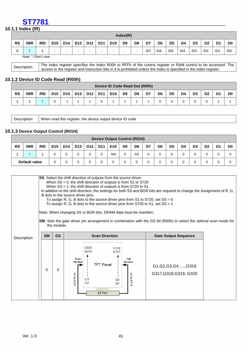
10.1.1 Index (IR) Index(IR)
RS /WR /RD D15 D14 D13 D12 D11 D10 D9 D8 D7 D6 D5 D4 D3 D2 D1 D0
0 ↑ 1 - - - - - - - - ID7 ID6 ID5 ID4 ID3 ID2 ID1 ID0
Note: “-“Don’t care
Description The index register specifies the index R00h to RFFh of the control register or RAM control to be accessed. The access to the register and instruction bits in it is prohibited unless the index is specified in the index register.
10.1.2 Device ID Code Read (R00h)
Device ID Code Read Out (R00h)
RS /WR /RD D15 D14 D13 D12 D11 D10 D9 D8 D7 D6 D5 D4 D3 D2 D1 D0
1 1 ↑ 0 1 1 1 0 1 1 1 1 0 0 0 0 0 1 1
Description When read this register, the device output device ID code
10.1.3 Device Output Control (R01H)
Device Output Control (R01H)
RS /WR /RD D15 D14 D13 D12 D11 D10 D9 D8 D7 D6 D5 D4 D3 D2 D1 D0
1 ↑ 1 0 0 0 0 0 SM 0 SS 0 0 0 0 0 0 0 0
Default value 0 0 0 0 0 0 0 0 0 0 0 0 0 0 0 0
Description
SS: Select the shift direction of outputs from the source driver. When SS = 0, the shift direction of outputs is from S1 to S720 When SS = 1, the shift direction of outputs is from S720 to S1.
In addition to the shift direction, the settings for both SS and BGR bits are required to change the Assignment of R, G, B dots to the source driver pins.
To assign R, G, B dots to the source driver pins from S1 to S720, set SS = 0. To assign R, G, B dots to the source driver pins from S720 to S1, set SS = 1.
Note: When changing SS or BGR bits, DRAM data must be rewritten.
SM: Sets the gate driver pin arrangement in combination with the GS bit (R60h) to select the optimal scan mode for the module.
SM GS Scan Direction Gate Output Sequence
0 0
G1,G2,G3,G4…..,G316
G317,G318,G319, G320
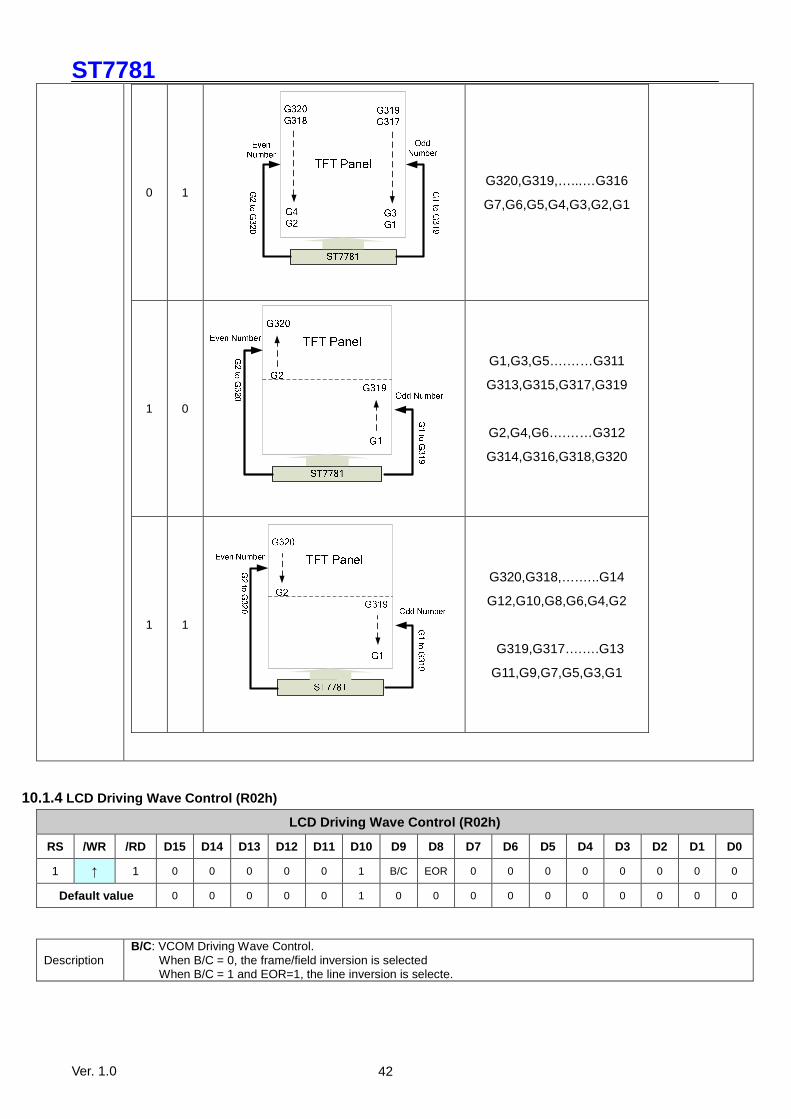
ST7781
Ver. 1.0 42
0 1
G320,G319,…...…G316
G7,G6,G5,G4,G3,G2,G1
1 0
G1,G3,G5….……G311
G313,G315,G317,G319
G2,G4,G6….……G312
G314,G316,G318,G320
1 1
G320,G318,….…..G14
G12,G10,G8,G6,G4,G2
G319,G317….….G13
G11,G9,G7,G5,G3,G1
10.1.4 LCD Driving Wave Control (R02h)
LCD Driving Wave Control (R02h)
RS /WR /RD D15 D14 D13 D12 D11 D10 D9 D8 D7 D6 D5 D4 D3 D2 D1 D0
1 ↑ 1 0 0 0 0 0 1 B/C EOR 0 0 0 0 0 0 0 0
Default value 0 0 0 0 0 1 0 0 0 0 0 0 0 0 0 0
Description B/C: VCOM Driving Wave Control.
When B/C = 0, the frame/field inversion is selected When B/C = 1 and EOR=1, the line inversion is selecte.
ST7781
Ver. 1.0 43
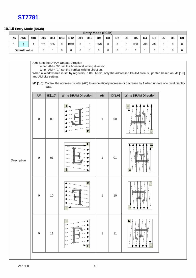
10.1.5 Entry Mode (R03h) Entry Mode (R03h)
RS /WR /RD D15 D14 D13 D12 D11 D10 D9 D8 D7 D6 D5 D4 D3 D2 D1 D0
1 ↑ 1 TRI DFM 0 BGR 0 0 HWN 0 0 0 I/D1 I/D0 AM 0 0 0
Default value 0 0 0 0 0 0 0 0 0 0 1 1 0 0 0 0
Description
AM: Sets the DRAM Updata Direction When AM = “0”, set the horizontal writing direction. When AM = “1”, set the vertical writing direction.
When a window area is set by registers R50h ~R53h, only the addressed DRAM area is updated based on I/D [1:0] and AM bits setting.
I/D [1:0] : Control the address counter (AC) to automatically increase or decrease by 1 when update one pixel display
data.
AM ID[1:0] Write DRAM Direction AM ID[1:0] Write DRAM Direction
0 00
1 00
0 01
1 01
0 10
1 10
0 11
1 11
ST7781
Ver. 1.0 44
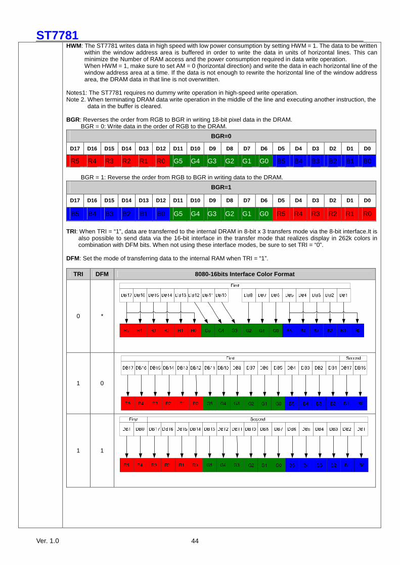
HWM: The ST7781 writes data in high speed with low power consumption by setting HWM = 1. The data to be written within the window address area is buffered in order to write the data in units of horizontal lines. This can minimize the Number of RAM access and the power consumption required in data write operation. When HWM = 1, make sure to set AM = 0 (horizontal direction) and write the data in each horizontal line of the window address area at a time. If the data is not enough to rewrite the horizontal line of the window address area, the DRAM data in that line is not overwritten.
Notes1: The ST7781 requires no dummy write operation in high-speed write operation. Note 2. When terminating DRAM data write operation in the middle of the line and executing another instruction, the
data in the buffer is cleared. BGR: Reverses the order from RGB to BGR in writing 18-bit pixel data in the DRAM.
BGR = 0: Write data in the order of RGB to the DRAM.
BGR=0
D17 D16 D15 D14 D13 D12 D11 D10 D9 D8 D7 D6 D5 D4 D3 D2 D1 D0
R5 R4 R3 R2 R1 R0 G5 G4 G3 G2 G1 G0 B5 B4 B3 B2 B1 B0 BGR = 1: Reverse the order from RGB to BGR in writing data to the DRAM.
BGR=1
D17 D16 D15 D14 D13 D12 D11 D10 D9 D8 D7 D6 D5 D4 D3 D2 D1 D0
B5 B4 B3 B2 B1 B0 G5 G4 G3 G2 G1 G0 R5 R4 R3 R2 R1 R0
TRI: When TRI = “1”, data are transferred to the internal DRAM in 8-bit x 3 transfers mode via the 8-bit interface.It is
also possible to send data via the 16-bit interface in the transfer mode that realizes display in 262k colors in combination with DFM bits. When not using these interface modes, be sure to set TRI = “0”.
DFM: Set the mode of transferring data to the internal RAM when TRI = “1”.
TRI DFM 8080-16bits Interface Color Format
0 *
1 0
1 1
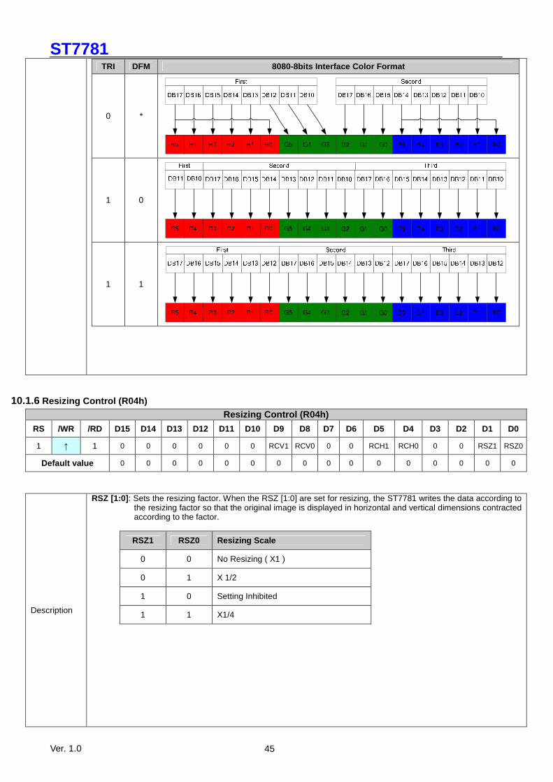
ST7781
Ver. 1.0 45
TRI DFM 8080-8bits Interface Color Format
0 *
1 0
1 1
10.1.6 Resizing Control (R04h) Resizing Control (R04h)
RS /WR /RD D15 D14 D13 D12 D11 D10 D9 D8 D7 D6 D5 D4 D3 D2 D1 D0
1 ↑ 1 0 0 0 0 0 0 RCV1 RCV0 0 0 RCH1 RCH0 0 0 RSZ1 RSZ0
Default value 0 0 0 0 0 0 0 0 0 0 0 0 0 0 0 0
Description
RSZ [1:0] : Sets the resizing factor. When the RSZ [1:0] are set for resizing, the ST7781 writes the data according to the resizing factor so that the original image is displayed in horizontal and vertical dimensions contracted according to the factor.
RSZ1 RSZ0 Resizing Scale
0 0 No Resizing ( X1 )
0 1 X 1/2
1 0 Setting Inhibited
1 1 X1/4
ST7781
Ver. 1.0 46
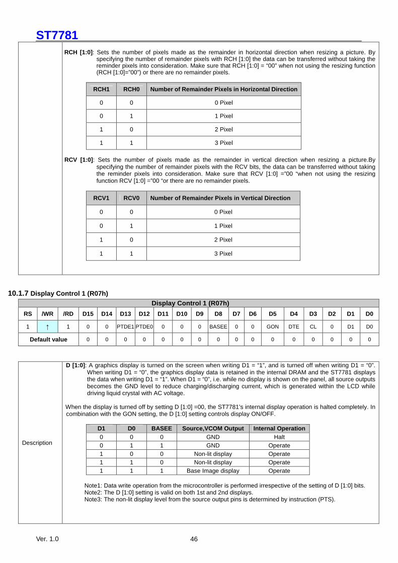
RCH [1:0] : Sets the number of pixels made as the remainder in horizontal direction when resizing a picture. By
specifying the number of remainder pixels with RCH [1:0] the data can be transferred without taking the reminder pixels into consideration. Make sure that RCH [1:0] = “00” when not using the resizing function (RCH [1:0]=”00”) or there are no remainder pixels.
RCH1 RCH0 Number of Remainder Pixels in Horizontal Direction
0 0 0 Pixel
0 1 1 Pixel
1 0 2 Pixel
1 1 3 Pixel
RCV [1:0] : Sets the number of pixels made as the remainder in vertical direction when resizing a picture.By
specifying the number of remainder pixels with the RCV bits, the data can be transferred without taking the reminder pixels into consideration. Make sure that RCV [1:0] =”00 “when not using the resizing function RCV [1:0] =”00 “or there are no remainder pixels.
RCV1 RCV0 Number of Remainder Pixels in Vertical Direction
0 0 0 Pixel
0 1 1 Pixel
1 0 2 Pixel
1 1 3 Pixel
10.1.7 Display Control 1 (R07h)
Display Control 1 (R07h)
RS /WR /RD D15 D14 D13 D12 D11 D10 D9 D8 D7 D6 D5 D4 D3 D2 D1 D0
1 ↑ 1 0 0 PTDE1 PTDE0 0 0 0 BASEE 0 0 GON DTE CL 0 D1 D0
Default value 0 0 0 0 0 0 0 0 0 0 0 0 0 0 0 0
Description
D [1:0] : A graphics display is turned on the screen when writing D1 = “1”, and is turned off when writing D1 = “0”. When writing D1 = “0”, the graphics display data is retained in the internal DRAM and the ST7781 displays the data when writing D1 = “1”. When D1 = “0”, i.e. while no display is shown on the panel, all source outputs becomes the GND level to reduce charging/discharging current, which is generated within the LCD while driving liquid crystal with AC voltage.
When the display is turned off by setting D [1:0] =00, the ST7781’s internal display operation is halted completely. In combination with the GON setting, the D [1:0] setting controls display ON/OFF.
D1 D0 BASEE Source,VCOM Output Internal Operation 0 0 0 GND Halt 0 1 1 GND Operate 1 0 0 Non-lit display Operate 1 1 0 Non-lit display Operate 1 1 1 Base Image display Operate
Note1: Data write operation from the microcontroller is performed irrespective of the setting of D [1:0] bits. Note2: The D [1:0] setting is valid on both 1st and 2nd displays. Note3: The non-lit display level from the source output pins is determined by instruction (PTS).
ST7781
Ver. 1.0 47
CL: When CL = “1”, the ST7781 halt grayscale amplifiers to display 8-color with low power consumption. When setting 8-color display mode, follow the sequence of 8-color display mode setting.
CL Display color 0 262,144 1 8
Note: When CL = 1, do not write the data corresponding to the grayscales, for which the operation of amplifier is halted.
GON, DTE: The combination of GON and DTE settings set the output level form gate lines (G1 ~ G320).
GON DTE Gate Output 0 0 VGH 0 1 VGH 1 0 VGL 1 1 Normal display
BASEE : Base image display enable bit.
BASEE = 0: No base image is displayed. The ST7781 drives liquid crystal with non-lit display level or drives only partial image display areas.
BASEE = 1: A base image is displayed on the screen. PTDE [1:0] : Partial image 2 and Partial image 1 enable bits
PTDE1/0 = 0: turns off partial image. Only base image is displayed. PTDE1/0 = 1: turns on partial image.
ST7781
Ver. 1.0 48
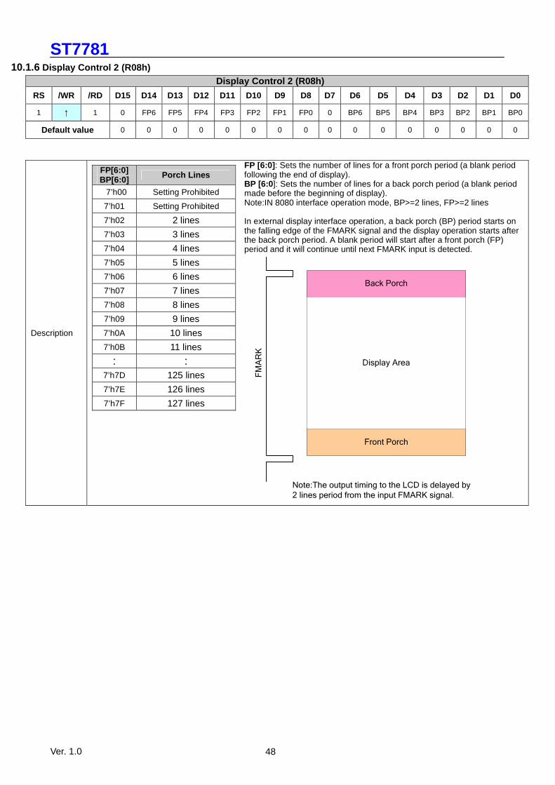
10.1.6 Display Control 2 (R08h) Display Control 2 (R08h)
RS /WR /RD D15 D14 D13 D12 D11 D10 D9 D8 D7 D6 D5 D4 D3 D2 D1 D0
1 ↑ 1 0 FP6 FP5 FP4 FP3 FP2 FP1 FP0 0 BP6 BP5 BP4 BP3 BP2 BP1 BP0
Default value 0 0 0 0 0 0 0 0 0 0 0 0 0 0 0 0
Description
FP [6:0] : Sets the number of lines for a front porch period (a blank period following the end of display). BP [6:0 ]: Sets the number of lines for a back porch period (a blank period made before the beginning of display). Note:IN 8080 interface operation mode, BP>=2 lines, FP>=2 lines In external display interface operation, a back porch (BP) period starts on the falling edge of the FMARK signal and the display operation starts after the back porch period. A blank period will start after a front porch (FP) period and it will continue until next FMARK input is detected.
Display Area
Back Porch
Front Porch
FMARK
Note:The output timing to the LCD is delayed by
2 lines period from the input FMARK signal.
FP[6:0] BP[6:0] Porch Lines
7’h00 Setting Prohibited
7’h01 Setting Prohibited
7’h02 2 lines
7’h03 3 lines
7’h04 4 lines
7’h05 5 lines
7’h06 6 lines
7’h07 7 lines
7’h08 8 lines
7’h09 9 lines
7’h0A 10 lines
7’h0B 11 lines
: : 7’h7D 125 lines
7’h7E 126 lines
7’h7F 127 lines
ST7781
Ver. 1.0 49
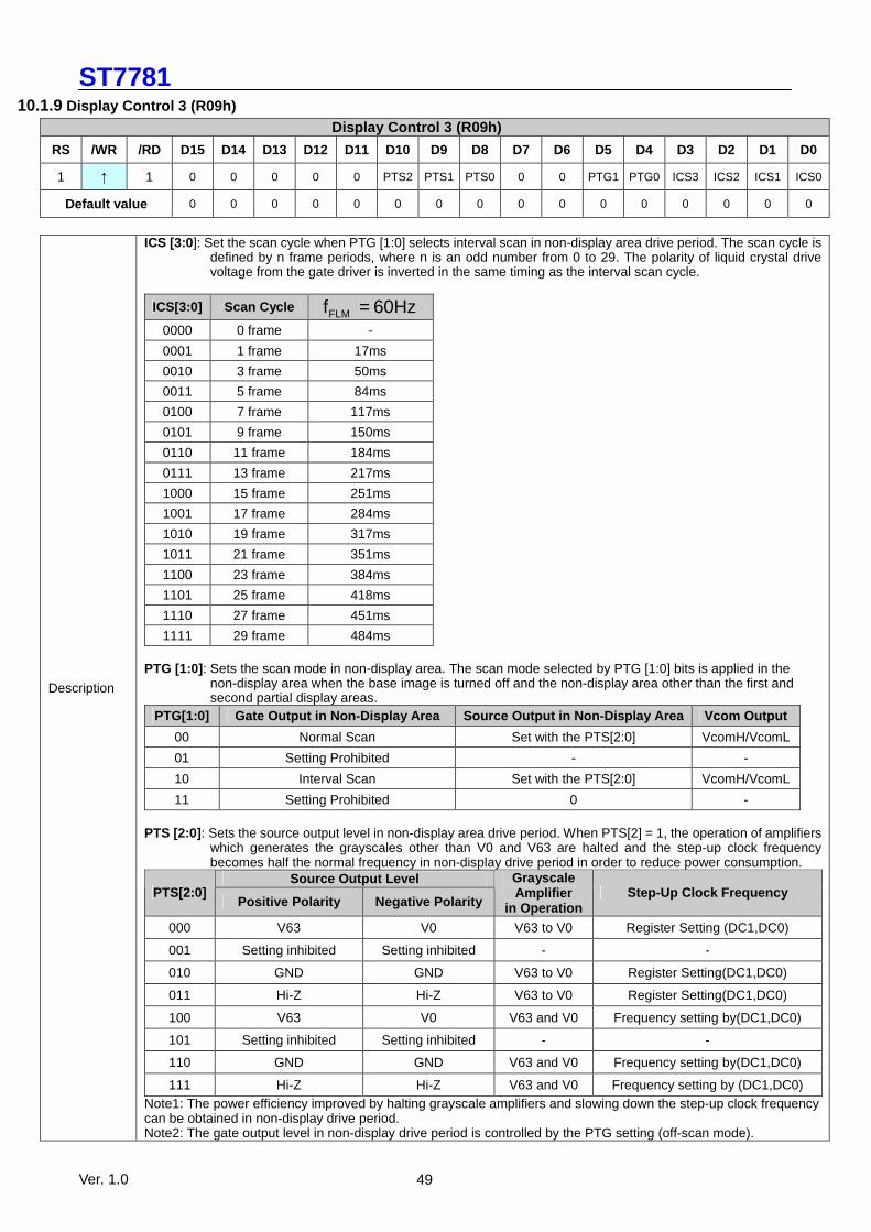
10.1.9 Display Control 3 (R09h)
Display Control 3 (R09h)
RS /WR /RD D15 D14 D13 D12 D11 D10 D9 D8 D7 D6 D5 D4 D3 D2 D1 D0
1 ↑ 1 0 0 0 0 0 PTS2 PTS1 PTS0 0 0 PTG1 PTG0 ICS3 ICS2 ICS1 ICS0
Default value 0 0 0 0 0 0 0 0 0 0 0 0 0 0 0 0
Description
ICS [3:0 ]: Set the scan cycle when PTG [1:0] selects interval scan in non-display area drive period. The scan cycle is defined by n frame periods, where n is an odd number from 0 to 29. The polarity of liquid crystal drive voltage from the gate driver is inverted in the same timing as the interval scan cycle.
ICS[3:0] Scan Cycle 60HzfFLM =
0000 0 frame -
0001 1 frame 17ms
0010 3 frame 50ms
0011 5 frame 84ms
0100 7 frame 117ms
0101 9 frame 150ms
0110 11 frame 184ms
0111 13 frame 217ms
1000 15 frame 251ms
1001 17 frame 284ms
1010 19 frame 317ms
1011 21 frame 351ms
1100 23 frame 384ms
1101 25 frame 418ms
1110 27 frame 451ms
1111 29 frame 484ms PTG [1:0] : Sets the scan mode in non-display area. The scan mode selected by PTG [1:0] bits is applied in the
non-display area when the base image is turned off and the non-display area other than the first and second partial display areas.
PTG[1:0] Gate Output in Non-Display Area Source Output in Non-Display Area Vcom Output
00 Normal Scan Set with the PTS[2:0] VcomH/VcomL
01 Setting Prohibited - -
10 Interval Scan Set with the PTS[2:0] VcomH/VcomL
11 Setting Prohibited 0 - PTS [2:0] : Sets the source output level in non-display area drive period. When PTS[2] = 1, the operation of amplifiers
which generates the grayscales other than V0 and V63 are halted and the step-up clock frequency becomes half the normal frequency in non-display drive period in order to reduce power consumption.
Source Output Level PTS[2:0]
Positive Polarity Negative Polarity
Grayscale Amplifier
in Operation Step-Up Clock Frequency
000 V63 V0 V63 to V0 Register Setting (DC1,DC0)
001 Setting inhibited Setting inhibited - -
010 GND GND V63 to V0 Register Setting(DC1,DC0)
011 Hi-Z Hi-Z V63 to V0 Register Setting(DC1,DC0)
100 V63 V0 V63 and V0 Frequency setting by(DC1,DC0)
101 Setting inhibited Setting inhibited - -
110 GND GND V63 and V0 Frequency setting by(DC1,DC0)
111 Hi-Z Hi-Z V63 and V0 Frequency setting by (DC1,DC0) Note1: The power efficiency improved by halting grayscale amplifiers and slowing down the step-up clock frequency can be obtained in non-display drive period. Note2: The gate output level in non-display drive period is controlled by the PTG setting (off-scan mode).
ST7781
Ver. 1.0 50
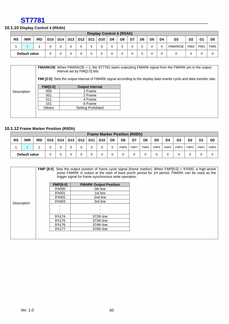
10.1.10 Display Control 4 (R0Ah)
Display Control 4 (R0Ah)
RS /WR /RD D15 D14 D13 D12 D11 D10 D9 D8 D7 D6 D5 D4 D3 D2 D1 D0
1 ↑ 1 0 0 0 0 0 0 0 0 0 0 0 0 FMARKOE FMI2 FMI1 FMI0
Default value 0 0 0 0 0 0 0 0 0 0 0 0 0 0 0 0
Description
FMARKOE : When FMARKOE = 1, the ST7781 starts outputting FMARK signal from the FMARK pin in the output interval set by FMI[2:0] bits
FMI [2:0] : Sets the output interval of FMARK signal according to the display data rewrite cycle and data transfer rate.
FMI[2:0] Output Interval 000 1 Frame 001 2 Frame 011 4 Frame 101 6 Frame
Others Setting Prohibited
10.1.12 Frame Marker Position (R0Dh)
Frame Marker Position (R0Dh)
RS /WR /RD D15 D14 D13 D12 D11 D10 D9 D8 D7 D6 D5 D4 D3 D2 D1 D0
1 ↑ 1 0 0 0 0 0 0 0 FMP8 FMP7 FMP6 FMP5 FMP4 FMP3 FMP2 FMP1 FMP0
Default value 0 0 0 0 0 0 0 0 0 0 0 0 0 0 0 0
Description
FMP [8:0 ]: Sets the output position of frame cycle signal (frame marker). When FMP[8:0] = 9’h000, a high-active pulse FMARK is output at the start of back porch period for 1H period. FMARK can be used as the trigger signal for frame synchronous write operation.
FMP[8:0] FMARK Output Position 9’h000 0th line 9’h001 1st line 9’h002 2nd line 9’h003 3rd line
.
.
.
.
.
. 9’h174 372th line 9’h175 373th line 9’h176 374th line 9’h177 375th line
ST7781
Ver. 1.0 51
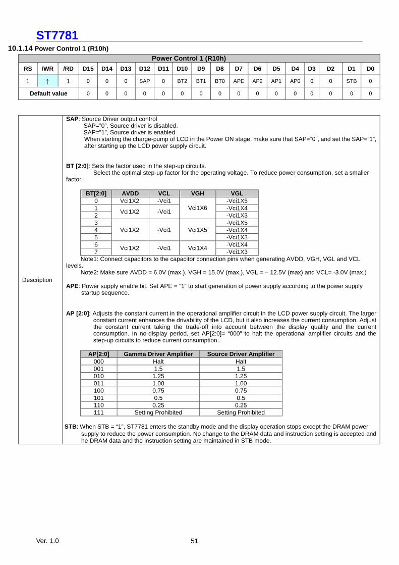
10.1.14 Power Control 1 (R10h)
Power Control 1 (R10h)
RS /WR /RD D15 D14 D13 D12 D11 D10 D9 D8 D7 D6 D5 D4 D3 D2 D1 D0
1 ↑ 1 0 0 0 SAP 0 BT2 BT1 BT0 APE AP2 AP1 AP0 0 0 STB 0
Default value 0 0 0 0 0 0 0 0 0 0 0 0 0 0 0 0
Description
SAP: Source Driver output control SAP=”0”, Source driver is disabled. SAP=”1”, Source driver is enabled. When starting the charge-pump of LCD in the Power ON stage, make sure that SAP=”0”, and set the SAP=”1”, after starting up the LCD power supply circuit.
BT [2:0] : Sets the factor used in the step-up circuits.
Select the optimal step-up factor for the operating voltage. To reduce power consumption, set a smaller factor.
BT[2:0] AVDD VCL VGH VGL
0 Vci1X2 -Vci1 -Vci1X5 1 -Vci1X4 2
Vci1X2 -Vci1 Vci1X6
-Vci1X3 3 -Vci1X5 4 -Vci1X4 5
Vci1X2 -Vci1 Vci1X5 -Vci1X3
6 -Vci1X4 7
Vci1X2 -Vci1 Vci1X4 -Vci1X3
Note1: Connect capacitors to the capacitor connection pins when generating AVDD, VGH, VGL and VCL levels.
Note2: Make sure AVDD = 6.0V (max.), VGH = 15.0V (max.), VGL = – 12.5V (max) and VCL= -3.0V (max.)
APE: Power supply enable bit. Set APE = “1” to start generation of power supply according to the power supply startup sequence.
AP [2:0] : Adjusts the constant current in the operational amplifier circuit in the LCD power supply circuit. The larger constant current enhances the drivability of the LCD, but it also increases the current consumption. Adjust the constant current taking the trade-off into account between the display quality and the current consumption. In no-display period, set AP[2:0]= “000” to halt the operational amplifier circuits and the step-up circuits to reduce current consumption.
AP[2:0] Gamma Driver Amplifier Source Driver Amplifier
000 Halt Halt 001 1.5 1.5 010 1.25 1.25 011 1.00 1.00 100 0.75 0.75 101 0.5 0.5 110 0.25 0.25 111 Setting Prohibited Setting Prohibited
STB: When STB = “1”, ST7781 enters the standby mode and the display operation stops except the DRAM power
supply to reduce the power consumption. No change to the DRAM data and instruction setting is accepted and he DRAM data and the instruction setting are maintained in STB mode.
ST7781
Ver. 1.0 52
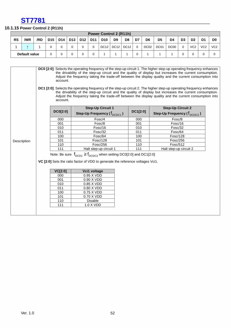
10.1.15 Power Control 2 (R11h)
Power Control 2 (R11h)
RS /WR /RD D15 D14 D13 D12 D11 D10 D9 D8 D7 D6 D5 D4 D3 D2 D1 D0
1 ↑ 1 0 0 0 0 0 DC12 DC12 DC12 0 DC02 DC01 DC00 0 VC2 VC2 VC2
Default value 0 0 0 0 0 1 1 1 0 1 1 1 0 0 0 0
Description
DC0 [2:0] : Selects the operating frequency of the step-up circuit 1. The higher step-up operating frequency enhances the drivability of the step-up circuit and the quality of display but increases the current consumption. Adjust the frequency taking the trade-off between the display quality and the current consumption into account.
DC1 [2:0] : Selects the operating frequency of the step-up circuit 2. The higher step-up operating frequency enhances
the drivability of the step-up circuit and the quality of display but increases the current consumption. Adjust the frequency taking the trade-off between the display quality and the current consumption into account.
DC0[2:0] Step-Up Circuit 1
Step-Up Frequency ( DCDC1f ) DC1[2:0] Step-Up Circuit 2
Step-Up Frequency ( DCDC2f )
000 Fosc/4 000 Fosc/8 001 Fosc/8 001 Fosc/16 010 Fosc/16 010 Fosc/32 011 Fosc/32 011 Fosc/64 100 Fosc/64 100 Fosc/128 101 Fosc/128 101 Fosc/256 110 Fosc/256 110 Fosc/512 111 Halt step-up circuit 1 111 Halt step-up circuit 2
Note: Be sure DCDC2DCD1 ff ≥ when setting DC0[2:0] and DC1[2:0]
VC [2:0] Sets the ratio factor of VDD to generate the reference voltages Vci1.
VC[2:0] Vci1 voltage
000 0.95 X VDD 001 0.90 X VDD 010 0.85 X VDD 011 0.80 X VDD 100 0.75 X VDD 101 0.70 X VDD 110 Disable 111 1.0 X VDD
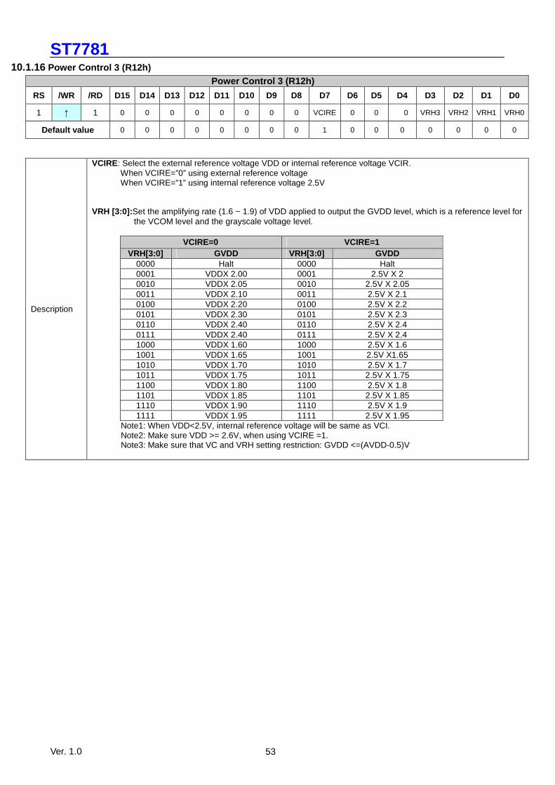
ST7781
Ver. 1.0 53
10.1.16 Power Control 3 (R12h)
Power Control 3 (R12h)
RS /WR /RD D15 D14 D13 D12 D11 D10 D9 D8 D7 D6 D5 D4 D3 D2 D1 D0
1 ↑ 1 0 0 0 0 0 0 0 0 VCIRE 0 0 0 VRH3 VRH2 VRH1 VRH0
Default value 0 0 0 0 0 0 0 0 1 0 0 0 0 0 0 0
Description
VCIRE: Select the external reference voltage VDD or internal reference voltage VCIR. When VCIRE=”0” using external reference voltage When VCIRE=”1” using internal reference voltage 2.5V VRH [3:0]: Set the amplifying rate (1.6 ~ 1.9) of VDD applied to output the GVDD level, which is a reference level for
the VCOM level and the grayscale voltage level.
VCIRE=0 VCIRE=1 VRH[3:0] GVDD VRH[3:0] GVDD
0000 Halt 0000 Halt 0001 VDDX 2.00 0001 2.5V X 2 0010 VDDX 2.05 0010 2.5V X 2.05 0011 VDDX 2.10 0011 2.5V X 2.1 0100 VDDX 2.20 0100 2.5V X 2.2 0101 VDDX 2.30 0101 2.5V X 2.3 0110 VDDX 2.40 0110 2.5V X 2.4 0111 VDDX 2.40 0111 2.5V X 2.4 1000 VDDX 1.60 1000 2.5V X 1.6 1001 VDDX 1.65 1001 2.5V X1.65 1010 VDDX 1.70 1010 2.5V X 1.7 1011 VDDX 1.75 1011 2.5V X 1.75 1100 VDDX 1.80 1100 2.5V X 1.8 1101 VDDX 1.85 1101 2.5V X 1.85 1110 VDDX 1.90 1110 2.5V X 1.9 1111 VDDX 1.95 1111 2.5V X 1.95
Note1: When VDD<2.5V, internal reference voltage will be same as VCI. Note2: Make sure VDD >= 2.6V, when using VCIRE =1. Note3: Make sure that VC and VRH setting restriction: GVDD <=(AVDD-0.5)V
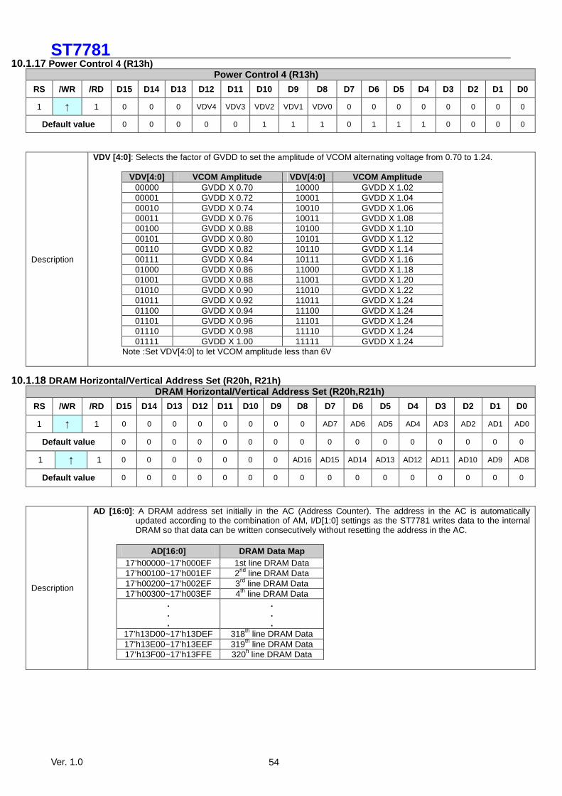
ST7781
Ver. 1.0 54
10.1.17 Power Control 4 (R13h) Power Control 4 (R13h)
RS /WR /RD D15 D14 D13 D12 D11 D10 D9 D8 D7 D6 D5 D4 D3 D2 D1 D0
1 ↑ 1 0 0 0 VDV4 VDV3 VDV2 VDV1 VDV0 0 0 0 0 0 0 0 0
Default value 0 0 0 0 0 1 1 1 0 1 1 1 0 0 0 0
Description
VDV [4:0] : Selects the factor of GVDD to set the amplitude of VCOM alternating voltage from 0.70 to 1.24.
VDV[4:0] VCOM Amplitude VDV[4:0] VCOM Amplitude 00000 GVDD X 0.70 10000 GVDD X 1.02 00001 GVDD X 0.72 10001 GVDD X 1.04 00010 GVDD X 0.74 10010 GVDD X 1.06 00011 GVDD X 0.76 10011 GVDD X 1.08 00100 GVDD X 0.88 10100 GVDD X 1.10 00101 GVDD X 0.80 10101 GVDD X 1.12 00110 GVDD X 0.82 10110 GVDD X 1.14 00111 GVDD X 0.84 10111 GVDD X 1.16 01000 GVDD X 0.86 11000 GVDD X 1.18 01001 GVDD X 0.88 11001 GVDD X 1.20 01010 GVDD X 0.90 11010 GVDD X 1.22 01011 GVDD X 0.92 11011 GVDD X 1.24 01100 GVDD X 0.94 11100 GVDD X 1.24 01101 GVDD X 0.96 11101 GVDD X 1.24 01110 GVDD X 0.98 11110 GVDD X 1.24 01111 GVDD X 1.00 11111 GVDD X 1.24
Note :Set VDV[4:0] to let VCOM amplitude less than 6V
10.1.18 DRAM Horizontal/Vertical Address Set (R20h, R21h)
DRAM Horizontal/Vertical Address Set (R20h,R21h)
RS /WR /RD D15 D14 D13 D12 D11 D10 D9 D8 D7 D6 D5 D4 D3 D2 D1 D0
1 ↑ 1 0 0 0 0 0 0 0 0 AD7 AD6 AD5 AD4 AD3 AD2 AD1 AD0
Default value 0 0 0 0 0 0 0 0 0 0 0 0 0 0 0 0
1 ↑ 1 0 0 0 0 0 0 0 AD16 AD15 AD14 AD13 AD12 AD11 AD10 AD9 AD8
Default value 0 0 0 0 0 0 0 0 0 0 0 0 0 0 0 0
Description
AD [16:0] : A DRAM address set initially in the AC (Address Counter). The address in the AC is automatically updated according to the combination of AM, I/D[1:0] settings as the ST7781 writes data to the internal DRAM so that data can be written consecutively without resetting the address in the AC.
AD[16:0] DRAM Data Map
17’h00000~17’h000EF 1st line DRAM Data 17’h00100~17’h001EF 2nd line DRAM Data 17’h00200~17’h002EF 3rd line DRAM Data 17’h00300~17’h003EF 4th line DRAM Data
.
.
.
.
.
. 17’h13D00~17’h13DEF 318th line DRAM Data 17’h13E00~17’h13EEF 319th line DRAM Data 17’h13F00~17’h13FFE 320h line DRAM Data

ST7781
Ver. 1.0 55
10.1.19 Write Data to DRAM (R22h) Write Data to DRAM (R22h)
RS /WR /RD D15 D14 D13 D12 D11 D10 D9 D8 D7 D6 D5 D4 D3 D2 D1 D0
1 ↑ 1 WD [17:0] - DRAM Write Data
Description
WD [17:0] : The ST7781 develops data into 18 bits internally in write operation. The format to develop data into 18 bits is different in different interface operation. The DRAM data represents the grayscale level. The DRAM data represents the grayscale level. ST7783 automatically updates the address to the begin point according to AM and I/D[1:0] settings as it’s wrote this register. The DFM bit sets the format to develop 16-bit data into the 18-bit data in 16-bit or 8-bit interface operation.
10.1.20 Read Data from DRAM (R22h)
Read Data from DRAM (R22h)
RS /WR /RD D15 D14 D13 D12 D11 D10 D9 D8 D7 D6 D5 D4 D3 D2 D1 D0
1 1 ↑ RD [17:0] - DRAM Read Data
Description
RD [17:0] : 18-bit data read from the DRAM. RAM read data RD [17:0] is transferred via different data bus in different interface operation. When the ST7781 reads data from the DRAM to the microcomputer, the first word read immediately after RAM address set is executed is taken in the internal read-data latch and invalid data is sent to the data bus. Valid data is sent to the data bus when the ST7781 reads out the second and subsequent words. When either 8-bit or 16-bit interface is selected, the LSBs of R and B dot data are not read out.
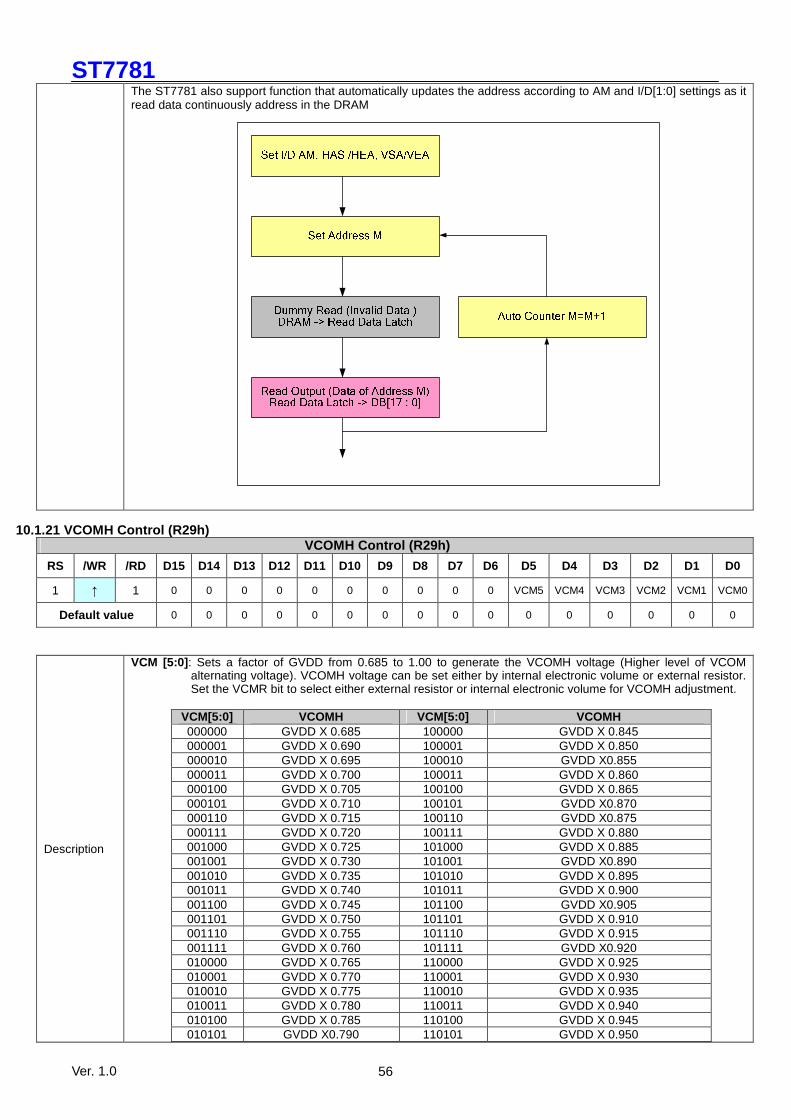
ST7781
Ver. 1.0 56
The ST7781 also support function that automatically updates the address according to AM and I/D[1:0] settings as it read data continuously address in the DRAM
10.1.21 VCOMH Control (R29h)
VCOMH Control (R29h)
RS /WR /RD D15 D14 D13 D12 D11 D10 D9 D8 D7 D6 D5 D4 D3 D2 D1 D0
1 ↑ 1 0 0 0 0 0 0 0 0 0 0 VCM5 VCM4 VCM3 VCM2 VCM1 VCM0
Default value 0 0 0 0 0 0 0 0 0 0 0 0 0 0 0 0
Description
VCM [5:0] : Sets a factor of GVDD from 0.685 to 1.00 to generate the VCOMH voltage (Higher level of VCOM alternating voltage). VCOMH voltage can be set either by internal electronic volume or external resistor. Set the VCMR bit to select either external resistor or internal electronic volume for VCOMH adjustment.
VCM[5:0] VCOMH VCM[5:0] VCOMH 000000 GVDD X 0.685 100000 GVDD X 0.845 000001 GVDD X 0.690 100001 GVDD X 0.850 000010 GVDD X 0.695 100010 GVDD X0.855 000011 GVDD X 0.700 100011 GVDD X 0.860 000100 GVDD X 0.705 100100 GVDD X 0.865 000101 GVDD X 0.710 100101 GVDD X0.870 000110 GVDD X 0.715 100110 GVDD X0.875 000111 GVDD X 0.720 100111 GVDD X 0.880 001000 GVDD X 0.725 101000 GVDD X 0.885 001001 GVDD X 0.730 101001 GVDD X0.890 001010 GVDD X 0.735 101010 GVDD X 0.895 001011 GVDD X 0.740 101011 GVDD X 0.900 001100 GVDD X 0.745 101100 GVDD X0.905 001101 GVDD X 0.750 101101 GVDD X 0.910 001110 GVDD X 0.755 101110 GVDD X 0.915 001111 GVDD X 0.760 101111 GVDD X0.920 010000 GVDD X 0.765 110000 GVDD X 0.925 010001 GVDD X 0.770 110001 GVDD X 0.930 010010 GVDD X 0.775 110010 GVDD X 0.935 010011 GVDD X 0.780 110011 GVDD X 0.940 010100 GVDD X 0.785 110100 GVDD X 0.945 010101 GVDD X0.790 110101 GVDD X 0.950

ST7781
Ver. 1.0 57
010110 GVDD X 0.795 110110 GVDD X 0.955 010111 GVDD X 0.800 110111 GVDD X 0.960 011000 GVDD X0.805 111000 GVDD X 0.965 011001 GVDD X0.810 111001 GVDD X 0.970 011010 GVDD X 0.815 111010 GVDD X 0.975 011011 GVDD X 0.820 111011 GVDD X 0.980 011100 GVDD X0.825 111100 GVDD X 0.985 011101 GVDD X 0.830 111101 GVDD X 0.990 011110 GVDD X 0.835 111110 GVDD X 0.995 011111 GVDD X0.840 111111 GVDD X 1.000
10.1.22 Frame Rate and Color Control (R2Bh) Frame Rate and Color Control (R2Bh)
RS /WR /RD D15 D14 D13 D12 D11 D10 D9 D8 D7 D6 D5 D4 D3 D2 D1 D0
1 ↑ 1 0 0 0 0 0 0 0 0 0 0 0 0 FRS3 FRS2 FRS1 FRS0
Default value 0 0 0 0 0 0 0 0 0 0 0 0 1 0 0 0
Description
FRS[3:0] :Set the frame rate when the internal resistor is used for oscillator circuit.
FRS[3:0] Frame Rate
0000 27.5 0001 29.3 0010 33 0011 36.7 0100 40.3 0101 44 0110 47.7 0111 51.3 1000 55 1001 64.2 1010 73.3 1011 82.5 1100 91.7 1101 100.8 1110 110 1111 114.1
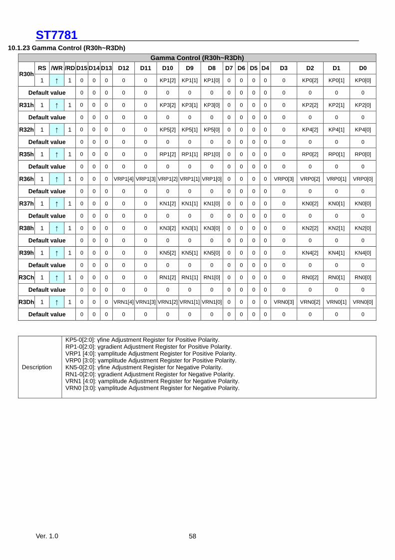
ST7781
Ver. 1.0 58
10.1.23 Gamma Control (R30h~R3Dh)
Gamma Control (R30h~R3Dh)
RS /WR /RD D15 D14 D13 D12 D11 D10 D9 D8 D7 D6 D5 D4 D3 D2 D1 D0 R30h
1 ↑ 1 0 0 0 0 0 KP1[2] KP1[1] KP1[0] 0 0 0 0 0 KP0[2] KP0[1] KP0[0]
Default value 0 0 0 0 0 0 0 0 0 0 0 0 0 0 0 0
R31h 1 ↑ 1 0 0 0 0 0 KP3[2] KP3[1] KP3[0] 0 0 0 0 0 KP2[2] KP2[1] KP2[0]
Default value 0 0 0 0 0 0 0 0 0 0 0 0 0 0 0 0
R32h 1 ↑ 1 0 0 0 0 0 KP5[2] KP5[1] KP5[0] 0 0 0 0 0 KP4[2] KP4[1] KP4[0]
Default value 0 0 0 0 0 0 0 0 0 0 0 0 0 0 0 0
R35h 1 ↑ 1 0 0 0 0 0 RP1[2] RP1[1] RP1[0] 0 0 0 0 0 RP0[2] RP0[1] RP0[0]
Default value 0 0 0 0 0 0 0 0 0 0 0 0 0 0 0 0
R36h 1 ↑ 1 0 0 0 VRP1[4] VRP1[3] VRP1[2] VRP1[1] VRP1[0] 0 0 0 0 VRP0[3] VRP0[2] VRP0[1] VRP0[0]
Default value 0 0 0 0 0 0 0 0 0 0 0 0 0 0 0 0
R37h 1 ↑ 1 0 0 0 0 0 KN1[2] KN1[1] KN1[0] 0 0 0 0 0 KN0[2] KN0[1] KN0[0]
Default value 0 0 0 0 0 0 0 0 0 0 0 0 0 0 0 0
R38h 1 ↑ 1 0 0 0 0 0 KN3[2] KN3[1] KN3[0] 0 0 0 0 0 KN2[2] KN2[1] KN2[0]
Default value 0 0 0 0 0 0 0 0 0 0 0 0 0 0 0 0
R39h 1 ↑ 1 0 0 0 0 0 KN5[2] KN5[1] KN5[0] 0 0 0 0 0 KN4[2] KN4[1] KN4[0]
Default value 0 0 0 0 0 0 0 0 0 0 0 0 0 0 0 0
R3Ch 1 ↑ 1 0 0 0 0 0 RN1[2] RN1[1] RN1[0] 0 0 0 0 0 RN0[2] RN0[1] RN0[0]
Default value 0 0 0 0 0 0 0 0 0 0 0 0 0 0 0 0
R3Dh 1 ↑ 1 0 0 0 VRN1[4] VRN1[3] VRN1[2] VRN1[1] VRN1[0] 0 0 0 0 VRN0[3] VRN0[2] VRN0[1] VRN0[0]
Default value 0 0 0 0 0 0 0 0 0 0 0 0 0 0 0 0
Description
KP5-0[2:0]: γfine Adjustment Register for Positive Polarity. RP1-0[2:0]: γgradient Adjustment Register for Positive Polarity. VRP1 [4:0]: γamplitude Adjustment Register for Positive Polarity. VRP0 [3:0]: γamplitude Adjustment Register for Positive Polarity. KN5-0[2:0]: γfine Adjustment Register for Negative Polarity. RN1-0[2:0]: γgradient Adjustment Register for Negative Polarity. VRN1 [4:0]: γamplitude Adjustment Register for Negative Polarity. VRN0 [3:0]: γamplitude Adjustment Register for Negative Polarity.
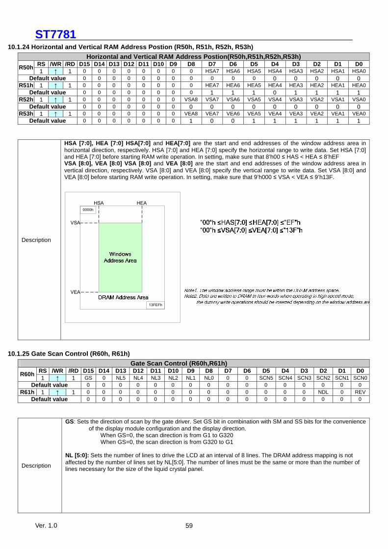
ST7781
Ver. 1.0 59
10.1.24 Horizontal and Vertical RAM Address Postion (R50h, R51h, R52h, R53h)
Horizontal and Vertical RAM Address Postion(R50h,R5 1h,R52h,R53h) RS /WR /RD D15 D14 D13 D12 D11 D10 D9 D8 D7 D6 D5 D4 D3 D2 D1 D0 R50h 1 ↑ 1 0 0 0 0 0 0 0 0 HSA7 HSA6 HSA5 HSA4 HSA3 HSA2 HSA1 HSA0
Default value 0 0 0 0 0 0 0 0 0 0 0 0 0 0 0 0 R51h 1 ↑ 1 0 0 0 0 0 0 0 0 HEA7 HEA6 HEA5 HEA4 HEA3 HEA2 HEA1 HEA0
Default value 0 0 0 0 0 0 0 0 1 1 1 0 1 1 1 1 R52h 1 ↑ 1 0 0 0 0 0 0 0 VSA8 VSA7 VSA6 VSA5 VSA4 VSA3 VSA2 VSA1 VSA0
Default value 0 0 0 0 0 0 0 0 0 0 0 0 0 0 0 0 R53h 1 ↑ 1 0 0 0 0 0 0 0 VEA8 VEA7 VEA6 VEA5 VEA4 VEA3 VEA2 VEA1 VEA0
Default value 0 0 0 0 0 0 0 1 0 0 1 1 1 1 1 1
Description
HSA [7:0], HEA [7:0] HSA[7:0] and HEA[7:0] are the start and end addresses of the window address area in horizontal direction, respectively. HSA [7:0] and HEA [7:0] specify the horizontal range to write data. Set HSA [7:0] and HEA [7:0] before starting RAM write operation. In setting, make sure that 8’h00 ≤ HAS < HEA ≤ 8’hEF VSA [8:0], VEA [8:0] VSA [8:0] and VEA [8:0] are the start and end addresses of the window address area in vertical direction, respectively. VSA [8:0] and VEA [8:0] specify the vertical range to write data. Set VSA [8:0] and VEA [8:0] before starting RAM write operation. In setting, make sure that 9’h000 ≤ VSA < VEA ≤ 9’h13F.
0000h
13FEFh
HSA HEA
VSA
VEA
10.1.25 Gate Scan Control (R60h, R61h)
Gate Scan Control (R60h,R61h) RS /WR /RD D15 D14 D13 D12 D11 D10 D9 D8 D7 D6 D5 D4 D3 D2 D1 D0 R60h 1 ↑ 1 GS 0 NL5 NL4 NL3 NL2 NL1 NL0 0 0 SCN5 SCN4 SCN3 SCN2 SCN1 SCN0
Default value 0 0 0 0 0 0 0 0 0 0 0 0 0 0 0 0 R61h 1 ↑ 1 0 0 0 0 0 0 0 0 0 0 0 0 0 NDL 0 REV
Default value 0 0 0 0 0 0 0 0 0 0 0 0 0 0 0 0
Description
GS: Sets the direction of scan by the gate driver. Set GS bit in combination with SM and SS bits for the convenience of the display module configuration and the display direction.
When GS=0, the scan direction is from G1 to G320 When GS=0, the scan direction is from G320 to G1
NL [5:0]: Sets the number of lines to drive the LCD at an interval of 8 lines. The DRAM address mapping is not affected by the number of lines set by NL[5:0]. The number of lines must be the same or more than the number of lines necessary for the size of the liquid crystal panel.
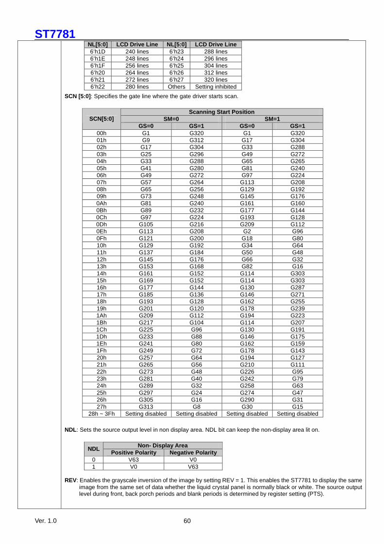
ST7781
Ver. 1.0 60
NL[5:0] LCD Drive Line NL[5:0] LCD Drive Line 6’h1D 240 lines 6’h23 288 lines 6’h1E 248 lines 6’h24 296 lines 6’h1F 256 lines 6’h25 304 lines 6’h20 264 lines 6’h26 312 lines 6’h21 272 lines 6’h27 320 lines 6’h22 280 lines Others Setting inhibited
SCN [5:0] : Specifies the gate line where the gate driver starts scan.
Scanning Start Position
SM=0 SM=1 SCN[5:0] GS=0 GS=1 GS=0 GS=1
00h G1 G320 G1 G320 01h G9 G312 G17 G304 02h G17 G304 G33 G288 03h G25 G296 G49 G272 04h G33 G288 G65 G265 05h G41 G280 G81 G240 06h G49 G272 G97 G224 07h G57 G264 G113 G208 08h G65 G256 G129 G192 09h G73 G248 G145 G176 0Ah G81 G240 G161 G160 0Bh G89 G232 G177 G144 0Ch G97 G224 G193 G128 0Dh G105 G216 G209 G112 0Eh G113 G208 G2 G96 0Fh G121 G200 G18 G80 10h G129 G192 G34 G64 11h G137 G184 G50 G48 12h G145 G176 G66 G32 13h G153 G168 G82 G16 14h G161 G152 G114 G303 15h G169 G152 G114 G303 16h G177 G144 G130 G287 17h G185 G136 G146 G271 18h G193 G128 G162 G255 19h G201 G120 G178 G239 1Ah G209 G112 G194 G223 1Bh G217 G104 G114 G207 1Ch G225 G96 G130 G191 1Dh G233 G88 G146 G175 1Eh G241 G80 G162 G159 1Fh G249 G72 G178 G143 20h G257 G64 G194 G127 21h G265 G56 G210 G111 22h G273 G48 G226 G95 23h G281 G40 G242 G79 24h G289 G32 G258 G63 25h G297 G24 G274 G47 26h G305 G16 G290 G31 27h G313 G8 G30 G15
28h ~ 3Fh Setting disabled Setting disabled Setting disabled Setting disabled
NDL: Sets the source output level in non display area. NDL bit can keep the non-display area lit on.
Non- Display Area NDL
Positive Polarity Negative Polarity 0 V63 V0 1 V0 V63
REV: Enables the grayscale inversion of the image by setting REV = 1. This enables the ST7781 to display the same
image from the same set of data whether the liquid crystal panel is normally black or white. The source output level during front, back porch periods and blank periods is determined by register setting (PTS).
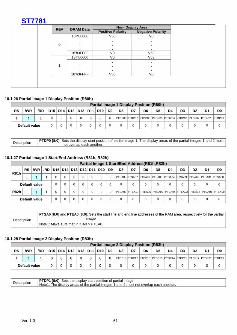
ST7781
Ver. 1.0 61
Non- Display Area REV DRAM Data Positive Polarity Negative Polarity
18’h00000 V63 V0 . . .
.
.
.
.
.
. 0
18’h3FFFF V0 V63 18’h00000 V0 V63
.
.
.
.
.
.
.
.
. 1
18’h3FFFF V63 V0
10.1.26 Partial Image 1 Display Position (R80h)
Partial Image 1 Display Position (R80h)
RS /WR /RD D15 D14 D13 D12 D11 D10 D9 D8 D7 D6 D5 D4 D3 D2 D1 D0
1 ↑ 1 0 0 0 0 0 0 0 PTDP08 PTDP07 PTDP06 PTDP05 PTDP04 PTDP03 PTDP02 PTDP01 PTDP00
Default value 0 0 0 0 0 0 0 0 0 0 0 0 0 0 0 0
Description PTDP0 [8:0] : Sets the display start position of partial image 1. The display areas of the partial images 1 and 2 must not overlap each another.
10.1.27 Partial Image 1 Start/End Address (R81h, R8 2h)
Partial Image 1 Start/End Address(R81h,R82h)
RS /WR /RD D15 D14 D13 D12 D11 D10 D9 D8 D7 D6 D5 D4 D3 D2 D1 D0 R81h
1 ↑ 1 0 0 0 0 0 0 0 PTSA08 PTSA07 PTSA06 PTSA05 PTSA04 PTSA03 PTSA02 PTSA01 PTSA00
Default value 0 0 0 0 0 0 0 0 0 0 0 0 0 0 0 0
R82h 1 ↑ 1 0 0 0 0 0 0 0 PTEA08 PTEA07 PTEA06 PTEA05 PTEA04 PTEA03 PTEA02 PTEA01 PTEA00
Default value 0 0 0 0 0 0 0 0 0 0 0 0 0 0 0 0
Description
PTSA0 [8:0] and PTEA0 [8:0] : Sets the start line and end line addresses of the RAM area, respectively for the partial image
Note1: Make sure that PTSA0 ≤ PTEA0.
10.1.28 Partial Image 2 Display Position (R83h)
Partial Image 2 Display Position (R83h)
RS /WR /RD D15 D14 D13 D12 D11 D10 D9 D8 D7 D6 D5 D4 D3 D2 D1 D0
1 ↑ 1 0 0 0 0 0 0 0 PTDP18 PTDP17 PTDP16 PTDP15 PTDP14 PTDP13 PTDP12 PTDP11 PTDP10
Default value 0 0 0 0 0 0 0 0 0 0 0 0 0 0 0 0
Description PTDP1 [8:0] : Sets the display start position of partial image Note1. The display areas of the partial images 1 and 2 must not overlap each another.
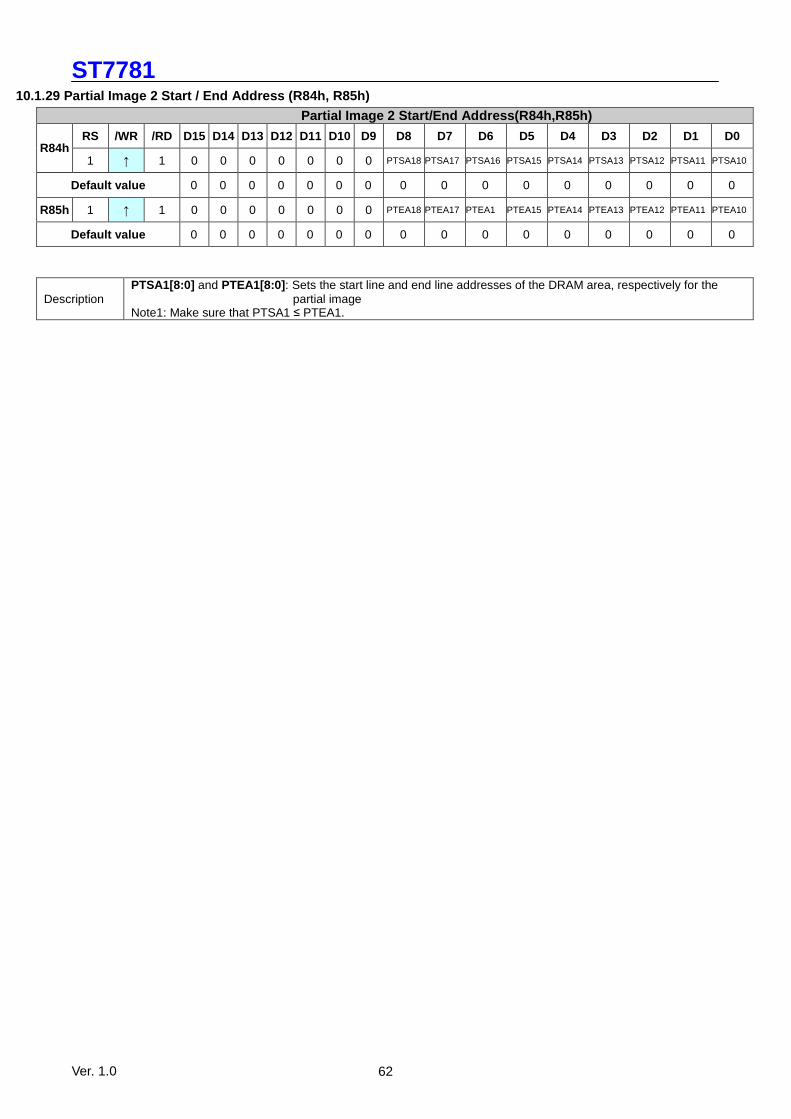
ST7781
Ver. 1.0 62
10.1.29 Partial Image 2 Start / End Address (R84h, R85h)
Partial Image 2 Start/End Address(R84h,R85h)
RS /WR /RD D15 D14 D13 D12 D11 D10 D9 D8 D7 D6 D5 D4 D3 D2 D1 D0 R84h
1 ↑ 1 0 0 0 0 0 0 0 PTSA18 PTSA17 PTSA16 PTSA15 PTSA14 PTSA13 PTSA12 PTSA11 PTSA10
Default value 0 0 0 0 0 0 0 0 0 0 0 0 0 0 0 0
R85h 1 ↑ 1 0 0 0 0 0 0 0 PTEA18 PTEA17 PTEA1 PTEA15 PTEA14 PTEA13 PTEA12 PTEA11 PTEA10
Default value 0 0 0 0 0 0 0 0 0 0 0 0 0 0 0 0
Description PTSA1[8:0] and PTEA1[8:0] : Sets the start line and end line addresses of the DRAM area, respectively for the
partial image Note1: Make sure that PTSA1 ≤ PTEA1.
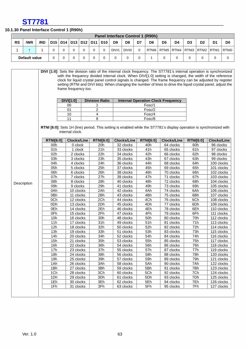
ST7781
Ver. 1.0 63
10.1.30 Panel Interface Control 1 (R90h)
Panel Interface Control 1 (R90h)
RS /WR /RD D15 D14 D13 D12 D11 D10 D9 D8 D7 D6 D5 D4 D3 D2 D1 D0
1 ↑ 1 0 0 0 0 0 0 DIVI1 DIVI0 0 RTNI6 RTNI5 RTNI4 RTNI3 RTNI2 RTNI1 RTNI0
Default value 0 0 0 0 0 0 0 0 0 1 0 0 0 0 0 0
Description
DIVI [1:0] : Sets the division ratio of the internal clock frequency. The ST7781’s internal operation is synchronized with the frequency divided internal clock. When DIVI[1:0] setting is changed, the width of the reference clock for liquid crystal panel control signals is changed. The frame frequency can be adjusted by register setting (RTNI and DIVI bits). When changing the number of lines to drive the liquid crystal panel, adjust the frame frequency too.
DIVI[1:0] Division Ratio Internal Operation Clock Frequency
00 1 Fosc/1 01 2 Fosc/2 10 4 Fosc/4 11 8 Fosc/8
RTNI [6:0] : Sets 1H (line) period. This setting is enabled while the ST7781’s display operation is synchronized with
internal clock.
RTNI[6:0] Clocks/Line RTNI[6:0] Clocks/Line RTNI[6:0] Clocks/Line RTNI[6:0] Clocks/Line 00h 0 clock 20h 32 clocks 40h 64 clocks 60h 96 clocks 01h 1 clock 21h 33 clocks 41h 65 clocks 61h 97 clocks 02h 2 clocks 22h 34 clocks 42h 66 clocks 62h 98 clocks 03h 3 clocks 23h 35 clocks 43h 67 clocks 63h 99 clocks 04h 4 clocks 24h 36 clocks 44h 68 clocks 64h 100 clocks 05h 5 clocks 25h 37 clocks 45h 69 clocks 65h 101 clocks 06h 6 clocks 26h 38 clocks 46h 70 clocks 66h 102 clocks 07h 7 clocks 27h 39 clocks 47h 71 clocks 67h 103 clocks 08h 8 clocks 28h 40 clocks 48h 72 clocks 68h 104 clocks 09h 9 clocks 29h 41 clocks 49h 73 clocks 69h 105 clocks 0Ah 10 clocks 2Ah 42 clocks 4Ah 74 clocks 6Ah 106 clocks 0Bh 11 clocks 2Bh 43 clocks 4Bh 75 clocks 6Bh 107 clocks 0Ch 12 clocks 2Ch 44 clocks 4Ch 76 clocks 6Ch 108 clocks 0Dh 13 clocks 2Dh 45 clocks 4Dh 77 clocks 6Dh 109 clocks 0Eh 14 clocks 2Eh 46 clocks 4Eh 78 clocks 6Eh 110 clocks 0Fh 15 clocks 2Fh 47 clocks 4Fh 79 clocks 6Fh 111 clocks 10h 16 clocks 30h 48 clocks 50h 80 clocks 70h 112 clocks 11h 17 clocks 31h 49 clocks 51h 81 clocks 71h 113 clocks 12h 18 clocks 32h 50 clocks 52h 82 clocks 72h 114 clocks 13h 19 clocks 33h 51 clocks 53h 83 clocks 73h 115 clocks 14h 20 clocks 34h 52 clocks 54h 84 clocks 74h 116 clocks 15h 21 clocks 35h 53 clocks 55h 85 clocks 75h 117 clocks 16h 22 clocks 36h 54 clocks 56h 86 clocks 76h 118 clocks 17h 23 clocks 37h 55 clocks 57h 87 clocks 77h 119 clocks 18h 24 clocks 38h 56 clocks 58h 88 clocks 78h 120 clocks 19h 25 clocks 39h 57 clocks 59h 89 clocks 79h 121 clocks 1Ah 26 clocks 3Ah 58 clocks 5Ah 90 clocks 7Ah 122 clocks 1Bh 27 clocks 3Bh 59 clocks 5Bh 91 clocks 7Bh 123 clocks 1Ch 28 clocks 3Ch 60 clocks 5Ch 92 clocks 7Ch 124 clocks 1Dh 29 clocks 3Dh 61 clocks 5Dh 93 clocks 7Dh 125 clocks 1Eh 30 clocks 3Eh 62 clocks 5Eh 94 clocks 7Eh 126 clocks 1Fh 31 clocks 3Fh 63 clocks 5Fh 95 clocks 7Fh 127 clocks
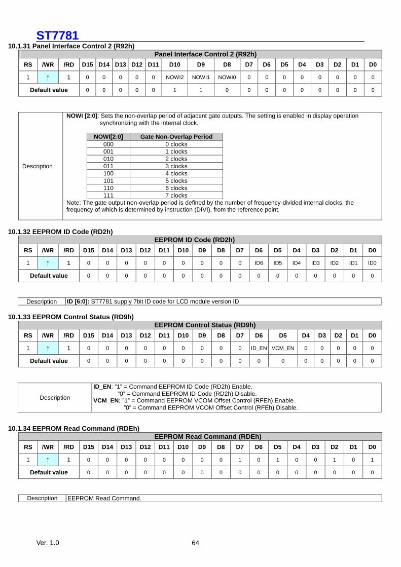
ST7781
Ver. 1.0 64
10.1.31 Panel Interface Control 2 (R92h) Panel Interface Control 2 (R92h)
RS /WR /RD D15 D14 D13 D12 D11 D10 D9 D8 D7 D6 D5 D4 D3 D2 D1 D0
1 ↑ 1 0 0 0 0 0 NOWI2 NOWI1 NOWI0 0 0 0 0 0 0 0 0
Default value 0 0 0 0 0 1 1 0 0 0 0 0 0 0 0 0
Description
NOWI [2:0] : Sets the non-overlap period of adjacent gate outputs. The setting is enabled in display operation synchronizing with the internal clock.
NOWI[2:0] Gate Non-Overlap Period
000 0 clocks 001 1 clocks 010 2 clocks 011 3 clocks 100 4 clocks 101 5 clocks 110 6 clocks 111 7 clocks
Note: The gate output non-overlap period is defined by the number of frequency-divided internal clocks, the frequency of which is determined by instruction (DIVI), from the reference point.
10.1.32 EEPROM ID Code (RD2h)
EEPROM ID Code (RD2h) RS /WR /RD D15 D14 D13 D12 D11 D10 D9 D8 D7 D6 D5 D4 D3 D2 D1 D0
1 ↑ 1 0 0 0 0 0 0 0 0 0 ID6 ID5 ID4 ID3 ID2 ID1 ID0
Default value 0 0 0 0 0 0 0 0 0 0 0 0 0 0 0 0
Description ID [6:0]: ST7781 supply 7bit ID code for LCD module version ID
10.1.33 EEPROM Control Status (RD9h) EEPROM Control Status (RD9h)
RS /WR /RD D15 D14 D13 D12 D11 D10 D9 D8 D7 D6 D5 D4 D3 D2 D1 D0
1 ↑ 1 0 0 0 0 0 0 0 0 0 ID_EN VCM_EN 0 0 0 0 0
Default value 0 0 0 0 0 0 0 0 0 0 0 0 0 0 0 0
Description
ID_EN: ”1” = Command EEPROM ID Code (RD2h) Enable. ”0” = Command EEPROM ID Code (RD2h) Disable.
VCM_EN: ”1” = Command EEPROM VCOM Offset Control (RFEh) Enable. ”0” = Command EEPROM VCOM Offset Control (RFEh) Disable.
10.1.34 EEPROM Read Command (RDEh) EEPROM Read Command (RDEh)
RS /WR /RD D15 D14 D13 D12 D11 D10 D9 D8 D7 D6 D5 D4 D3 D2 D1 D0
1 ↑ 1 0 0 0 0 0 0 0 0 1 0 1 0 0 1 0 1
Default value 0 0 0 0 0 0 0 0 0 0 0 0 0 0 0 0
Description EEPROM Read Command.
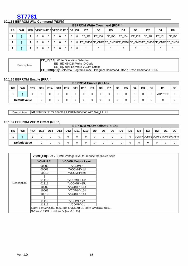
ST7781
Ver. 1.0 65
10.1.35 EEPROM Wite Command (RDFh) EEPROM Write Command (RDFh)
RS /WR /RD D15 D14 D13 D12 D11 D10 D9 D8 D7 D6 D5 D4 D3 D2 D1 D0
1 ↑ 1 0 0 0 0 0 0 0 0 EE_IB7 EE_IB6 EE_IB5 EE_IB4 EE_IB3 EE_IB2 EE_IB1 EE_IB0
1 ↑ 1 0 0 0 0 0 0 0 0 EE_CMD7 EE_CMD6 EE_CMD5 EE_CMD4 EE_CMD3 EE_CMD2 EE_CMD1 EE_CMD0
1 ↑ 1 0 0 0 0 0 0 0 0 1 0 1 0 0 1 0 1
Description
EE_IB[7:0] : Write Operation Selection. EE_IB[7:0]=D2h,Write ID Code
EE_IB[7:0]=FEh,Write VCOM Offest EE_CMD[7:0] : Select to Program/Erase ; Program Command : 3Ah ; Erase Command : C5h
10.1.36 EEPROM Enable (RFAh) EEPROM Enable (RFAh)
RS /WR /RD D15 D14 D13 D12 D11 D10 D9 D8 D7 D6 D5 D4 D3 D2 D1 D0
1 ↑ 1 0 0 0 0 0 0 0 0 0 0 0 0 0 0 MTPPROG 0
Default value 0 0 0 0 0 0 0 0 0 0 0 0 0 0 0 0
Description MTPPROG:”1” for enable EEPROM function with SW_EE =1
10.1.37 EEPROM VCOM Offset (RFEh) EEPROM VCOM Offset (RFEh)
RS /WR /RD D15 D14 D13 D12 D11 D10 D9 D8 D7 D6 D5 D4 D3 D2 D1 D0
1 ↑ 1 0 0 0 0 0 0 0 0 0 0 0 VCMF4 VCMF3 VCMF2 VCMF1 VCMF0
Default value 0 0 0 0 0 0 0 0 0 0 0 0 0 0 0 0
Description
VCMF[4:0]: Set VCOMH Voltage level for reduce the flicker issue
VCMF[4:0] VCOMH Output Level
00000 “VCOMH” 00001 “VCOMH”+1d 00010 “VCOMH”+2d
| | 01110 “VCOMH”+14d 01111 “VCOMH”+15d 10000 “VCOMH”-16d 10001 “VCOMH”-15d 10010 “VCOMH”-14d
| | 11110 “VCOMH”-2d 11111 “VCOMH”-1d
Note: 1d=GVDDX0.005, 2d= GVDDX0.01, 3d = GVDDX0.015.... 3V <= VCOMH + nd <=5V (n= -16~15)
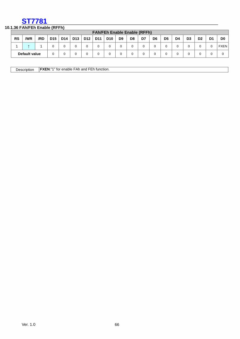
ST7781
Ver. 1.0 66
10.1.36 FAh/FEh Enable (RFFh) FAh/FEh Enable Enable (RFFh)
RS /WR /RD D15 D14 D13 D12 D11 D10 D9 D8 D7 D6 D5 D4 D3 D2 D1 D0
1 ↑ 1 0 0 0 0 0 0 0 0 0 0 0 0 0 0 0 FXEN
Default value 0 0 0 0 0 0 0 0 0 0 0 0 0 0 0 0
Description FXEN:”1” for enable FAh and FEh function.
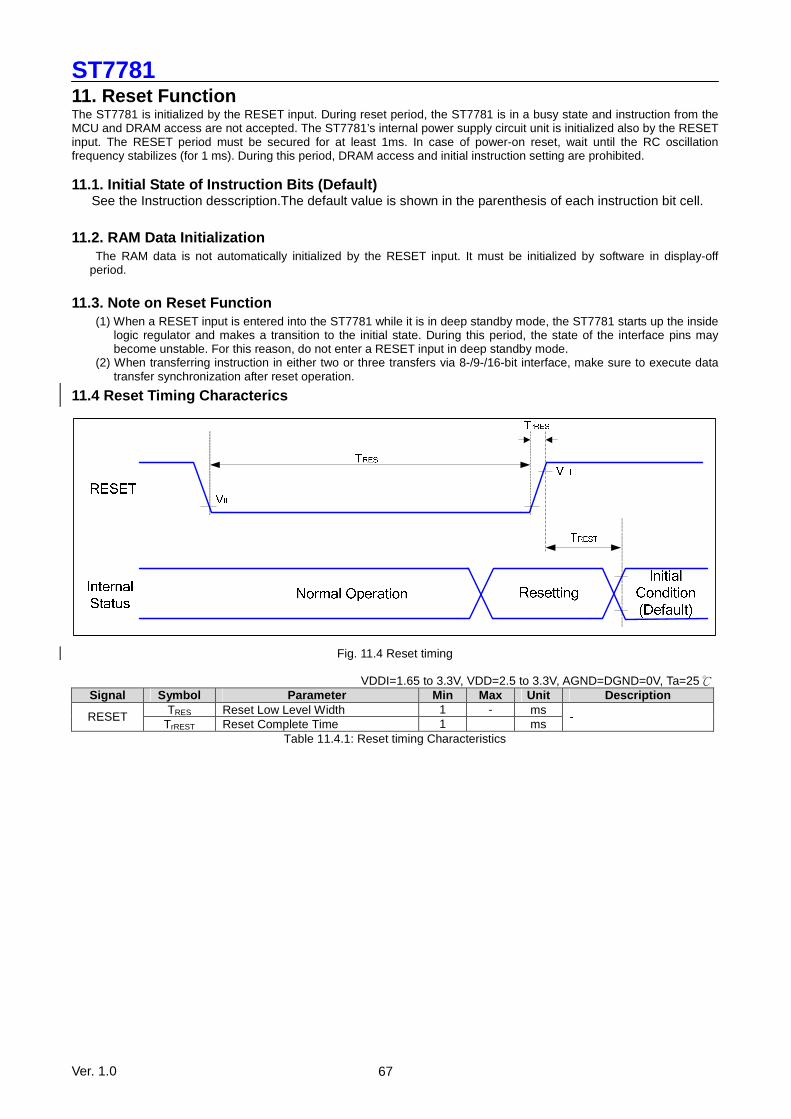
ST7781
Ver. 1.0 67
11. Reset Function The ST7781 is initialized by the RESET input. During reset period, the ST7781 is in a busy state and instruction from the MCU and DRAM access are not accepted. The ST7781’s internal power supply circuit unit is initialized also by the RESET input. The RESET period must be secured for at least 1ms. In case of power-on reset, wait until the RC oscillation frequency stabilizes (for 1 ms). During this period, DRAM access and initial instruction setting are prohibited.
11.1. Initial State of Instruction Bits (Default)
See the Instruction desscription.The default value is shown in the parenthesis of each instruction bit cell.
11.2. RAM Data Initialization The RAM data is not automatically initialized by the RESET input. It must be initialized by software in display-off
period.
11.3. Note on Reset Function (1) When a RESET input is entered into the ST7781 while it is in deep standby mode, the ST7781 starts up the inside
logic regulator and makes a transition to the initial state. During this period, the state of the interface pins may become unstable. For this reason, do not enter a RESET input in deep standby mode.
(2) When transferring instruction in either two or three transfers via 8-/9-/16-bit interface, make sure to execute data transfer synchronization after reset operation.
11.4 Reset Timing Characterics
Fig. 11.4 Reset timing
VDDI=1.65 to 3.3V, VDD=2.5 to 3.3V, AGND=DGND=0V, Ta=25℃ Signal Symbol Parameter Min Max Unit Description
TRES Reset Low Level Width 1 - ms RESET TrREST Reset Complete Time 1 ms
-
Table 11.4.1: Reset timing Characteristics
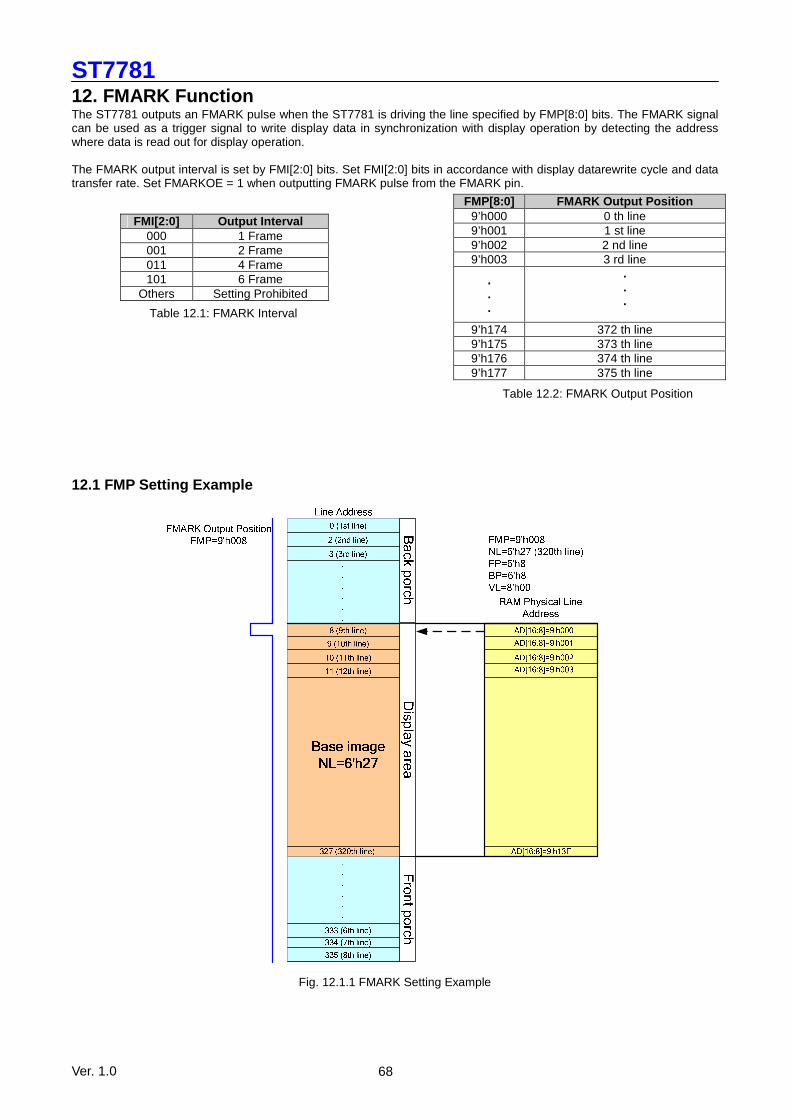
ST7781
Ver. 1.0 68
12. FMARK Function The ST7781 outputs an FMARK pulse when the ST7781 is driving the line specified by FMP[8:0] bits. The FMARK signal can be used as a trigger signal to write display data in synchronization with display operation by detecting the address where data is read out for display operation. The FMARK output interval is set by FMI[2:0] bits. Set FMI[2:0] bits in accordance with display datarewrite cycle and data transfer rate. Set FMARKOE = 1 when outputting FMARK pulse from the FMARK pin.
FMI[2:0] Output Interval
000 1 Frame 001 2 Frame 011 4 Frame 101 6 Frame
Others Setting Prohibited
Table 12.1: FMARK Interval
Table 12.2: FMARK Output Position
12.1 FMP Setting Example
Fig. 12.1.1 FMARK Setting Example
FMP[8:0] FMARK Output Position 9’h000 0 th line 9’h001 1 st line 9’h002 2 nd line 9’h003 3 rd line
.
.
.
.
.
.
9’h174 372 th line 9’h175 373 th line 9’h176 374 th line 9’h177 375 th line
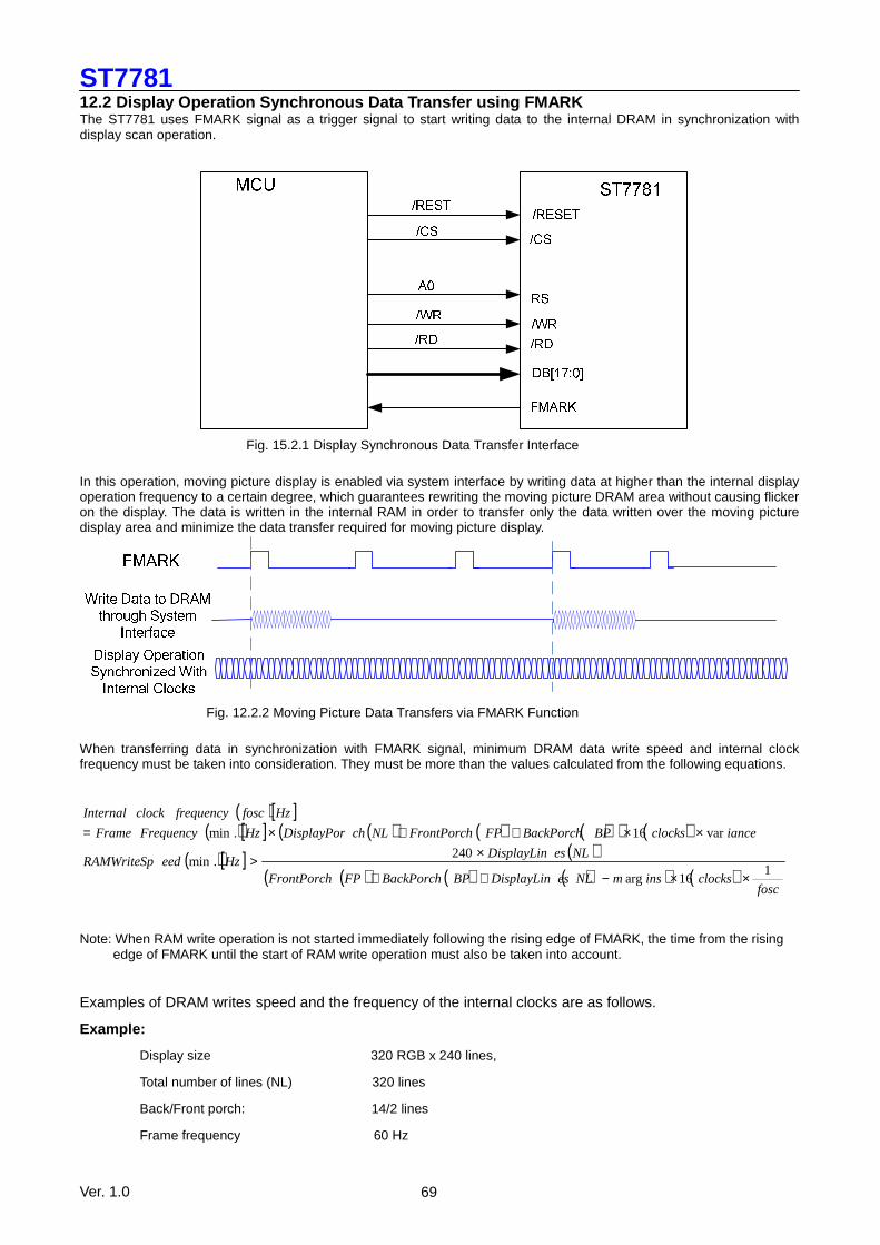
ST7781
Ver. 1.0 69
12.2 Display Operation Synchronous Data Transfer us ing FMARK The ST7781 uses FMARK signal as a trigger signal to start writing data to the internal DRAM in synchronization with display scan operation.
Fig. 15.2.1 Display Synchronous Data Transfer Interface
In this operation, moving picture display is enabled via system interface by writing data at higher than the internal display operation frequency to a certain degree, which guarantees rewriting the moving picture DRAM area without causing flicker on the display. The data is written in the internal RAM in order to transfer only the data written over the moving picture display area and minimize the data transfer required for moving picture display.
Fig. 12.2.2 Moving Picture Data Transfers via FMARK Function
When transferring data in synchronization with FMARK signal, minimum DRAM data write speed and internal clock frequency must be taken into consideration. They must be more than the values calculated from the following equations.
( )[ ]
( )[ ] ( ) ( ) ( )( ) ( )( )[ ] ( )
( ) ( ) ( )( ) ( )fosc
clocksinsmNLesDisplayLinBPBackPorchFPFrontPorch
NLesDisplayLinHzeedRAMWriteSp
ianceclocksBPBackPorchFPFrontPorchNLchDisplayPorHzFrequencyFrame
HzfoscfrequencyclockInternal
116arg
240.min
var16.min
××−++
×>
××++×=
Note: When RAM write operation is not started immediately following the rising edge of FMARK, the time from the rising
edge of FMARK until the start of RAM write operation must also be taken into account.
Examples of DRAM writes speed and the frequency of the internal clocks are as follows.
Example:
Display size 320 RGB x 240 lines,
Total number of lines (NL) 320 lines
Back/Front porch: 14/2 lines
Frame frequency 60 Hz
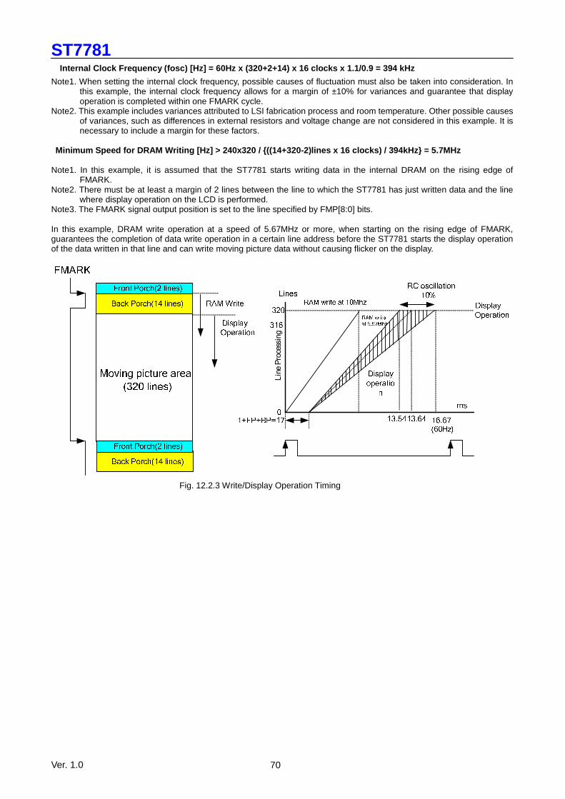
ST7781
Ver. 1.0 70
Internal Clock Frequency (fosc) [Hz] = 60Hz x (32 0+2+14) x 16 clocks x 1.1/0.9 = 394 kHz
Note1. When setting the internal clock frequency, possible causes of fluctuation must also be taken into consideration. In this example, the internal clock frequency allows for a margin of ±10% for variances and guarantee that display operation is completed within one FMARK cycle.
Note2. This example includes variances attributed to LSI fabrication process and room temperature. Other possible causes of variances, such as differences in external resistors and voltage change are not considered in this example. It is necessary to include a margin for these factors.
Minimum Speed for DRAM Writing [Hz] > 240x320 / {( (14+320-2)lines x 16 clocks) / 394kHz} = 5.7MHz Note1. In this example, it is assumed that the ST7781 starts writing data in the internal DRAM on the rising edge of
FMARK. Note2. There must be at least a margin of 2 lines between the line to which the ST7781 has just written data and the line
where display operation on the LCD is performed. Note3. The FMARK signal output position is set to the line specified by FMP[8:0] bits. In this example, DRAM write operation at a speed of 5.67MHz or more, when starting on the rising edge of FMARK, guarantees the completion of data write operation in a certain line address before the ST7781 starts the display operation of the data written in that line and can write moving picture data without causing flicker on the display.
LineProcessing
Fig. 12.2.3 Write/Display Operation Timing
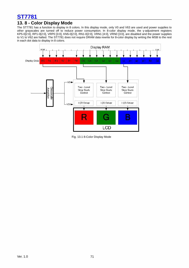
ST7781
Ver. 1.0 71
13. 8 - Color Display Mode The ST7781 has a function to display in 8 colors. In this display mode, only V0 and V63 are used and power supplies to other grayscales are turned off to reduce power consumption. In 8-color display mode, the γ-adjustment registers KP5-0[2:0], RP1-0[2:0], VRP0 [3:0], KN5-0[2:0], RN1-0[2:0], VRN1 [4:0], VRN0 [3:0], are disabled and the power supplies to V1 to V62 are halted. The ST7781 does not require DRAM data rewrite for 8-color display by writing the MSB to the rest in each dot data to display in 8 colors.
Fig. 13.1 8-Color Display Mode
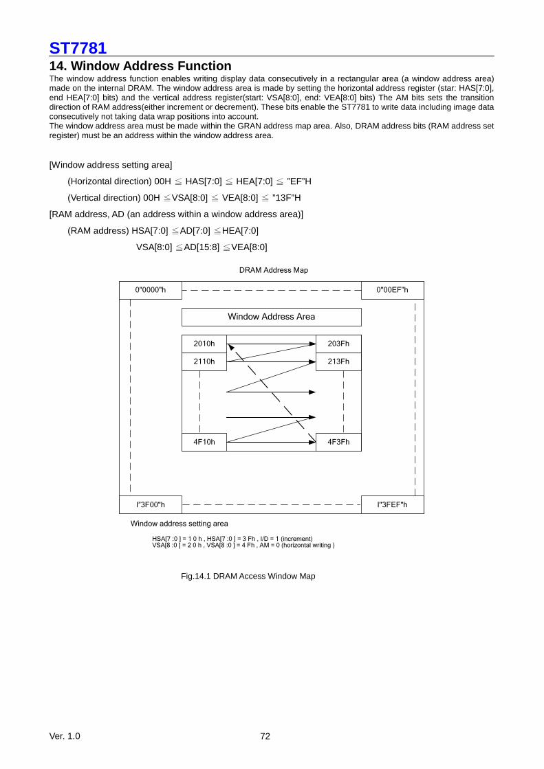
ST7781
Ver. 1.0 72
14. Window Address Function The window address function enables writing display data consecutively in a rectangular area (a window address area) made on the internal DRAM. The window address area is made by setting the horizontal address register (star: HAS[7:0], end HEA[7:0] bits) and the vertical address register(start: VSA[8:0], end: VEA[8:0] bits) The AM bits sets the transition direction of RAM address(either increment or decrement). These bits enable the ST7781 to write data including image data consecutively not taking data wrap positions into account. The window address area must be made within the GRAN address map area. Also, DRAM address bits (RAM address set register) must be an address within the window address area.
[Window address setting area]
(Horizontal direction) 00H HAS[7:0] HEA[7:0] ”EF”H≦ ≦ ≦
(Vertical direction) 00H VSA[8:0] VEA[8:0] ”13F”H≦ ≦ ≦
[RAM address, AD (an address within a window address area)]
(RAM address) HSA[7:0] AD[7:0] HEA[7:0]≦ ≦
VSA[8:0] AD[15:8] VEA[8:0]≦ ≦
0"0000"h 0"00EF”h
I”3F00"h I"3FEF"h
2010h 203Fh
4F10h 4F3Fh
2110h 213Fh
Window Address Area
Window address setting area
DRAM Address Map
HSA[7 :0 ] = 1 0 h , HSA[7 :0 ] = 3 Fh , I/D = 1 (increment)VSA[8 :0 ] = 2 0 h , VSA[8 :0 ] = 4 Fh , AM = 0 (horizontal writing )
Fig.14.1 DRAM Access Window Map

ST7781
Ver. 1.0 73
15. Gamma Correction ST7781 incorporate the γ- correction function to display 262,244 colors for the LCD panel. Theγ-correction is performed with 3 groups of registers determining eight reference grayscale levels, which are gradient adjustment, amplitude adjustment and fine- adjustment registers for positive and negative polarities, to make ST7781 available with liquid crystal panels of various characteristics.
Fig.15.1 Grayscale Voltage Generation
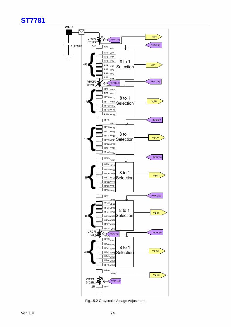
ST7781
Ver. 1.0 74
GVDD
1uF/10V
VRCP00~28R
5R
4R
VR0P00~30R
1R
1R
1R
1R
VRCP10~28R
VR0P10~31R
4R
8R
RP0
RP1
RP2
RP3
RP4
RP5
RP6
RP7
RP8
RP9
RP10
RP11
RP12
RP13
RP14
RP15
RP16
RP17
RP18
RP19
RP20
RP21
RP22
RP23
RP24
RP25
RP26
RP27
RP28
RP29
RP30
RP31
RP32
RP33
RP34
RP35
RP36
RP37
RP38
RP39
RP40
RP41
RP42
RP43
RP44
RP45
RP46
RP47
VP1
VP2
VP3
VP4
VP5
VP6
VP7
VP8
VP9
VP10
VP11
VP12
VP13
VP14
VP15
VP16
VP17
VP18
VP19
VP20
VP 21
VP22
VP23
VP24
VP25
VP26
VP27
VP28
VP29
VP30
VP31
VP32
VP33
VP34
VP35
VP36
VP37
VP38
VP39
VP40
VP41
VP42
VP43
VP44
VP45
VP46
VP47
VP48
VP49
VRPO[3:0]
PRPO[2:0]
VgP0
PKP0[2:0]
VgP1
PKP1[2:0]
VgP8
PKP2[2:0]
VgP20
PKP3[2:0]
VgP43
PKP4[2:0]
VgP55
PKP5[2:0]
VgP62
PRP1[2:0]
VRP1[4:0]
VgP63
8 to 1 Selection
8 to 1 Selection
8 to 1 Selection
8 to 1 Selection
8 to 1 Selection
8 to 1 Selection
Fig.15.2 Grayscale Voltage Adjustment
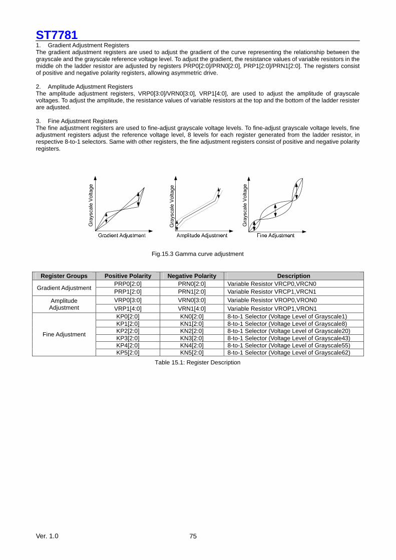
ST7781
Ver. 1.0 75
1. Gradient Adjustment Registers The gradient adjustment registers are used to adjust the gradient of the curve representing the relationship between the grayscale and the grayscale reference voltage level. To adjust the gradient, the resistance values of variable resistors in the middle oh the ladder resistor are adjusted by registers PRP0[2:0]/PRN0[2:0], PRP1[2:0]/PRN1[2:0]. The registers consist of positive and negative polarity registers, allowing asymmetric drive. 2. Amplitude Adjustment Registers The amplitude adjustment registers, VRP0[3:0]/VRN0[3:0], VRP1[4:0], are used to adjust the amplitude of grayscale voltages. To adjust the amplitude, the resistance values of variable resistors at the top and the bottom of the ladder resister are adjusted. 3. Fine Adjustment Registers The fine adjustment registers are used to fine-adjust grayscale voltage levels. To fine-adjust grayscale voltage levels, fine adjustment registers adjust the reference voltage level, 8 levels for each register generated from the ladder resistor, in respective 8-to-1 selectors. Same with other registers, the fine adjustment registers consist of positive and negative polarity registers.
Grayscale Voltage
Grayscale Voltage
Grayscale Voltage
Fig.15.3 Gamma curve adjustment
Register Groups Positive Polarity Negative Polarity Description PRP0[2:0] PRN0[2:0] Variable Resistor VRCP0,VRCN0
Gradient Adjustment PRP1[2:0] PRN1[2:0] Variable Resistor VRCP1,VRCN1 VRP0[3:0] VRN0[3:0] Variable Resistor VROP0,VRON0 Amplitude
Adjustment VRP1[4:0] VRN1[4:0] Variable Resistor VROP1,VRON1 KP0[2:0] KN0[2:0] 8-to-1 Selector (Voltage Level of Grayscale1) KP1[2:0] KN1[2:0] 8-to-1 Selector (Voltage Level of Grayscale8) KP2[2:0] KN2[2:0] 8-to-1 Selector (Voltage Level of Grayscale20) KP3[2:0] KN3[2:0] 8-to-1 Selector (Voltage Level of Grayscale43) KP4[2:0] KN4[2:0] 8-to-1 Selector (Voltage Level of Grayscale55)
Fine Adjustment
KP5[2:0] KN5[2:0] 8-to-1 Selector (Voltage Level of Grayscale62)
Table 15.1: Register Description
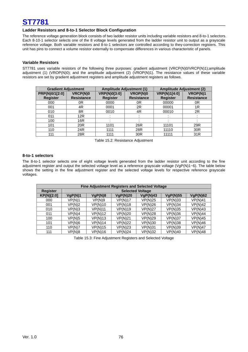
ST7781
Ver. 1.0 76
Ladder Resistors and 8-to-1 Selector Block Configur ation The reference voltage generation block consists of two ladder resistor units including variable resistors and 8-to-1 selectors. Each 8-10-1 selector selects one of the 8 voltage levels generated from the ladder resistor unit to output as a grayscale reference voltage. Both variable resistors and 8-to-1 selectors are controlled according to theγ-correction registers. This unit has pins to connect a volume resistor externally to compensate differences in various characteristic of panels.
Variable Resistors ST7781 uses variable resistors of the following three purposes: gradient adjustment (VRCP(N)0/VRCP(N)1);amplitude adjustment (1) (VROP(N)0); and the amplitude adjustment (2) (VROP(N)1). The resistance values of these variable resistors are set by gradient adjustment registers and amplitude adjustment registers as follows.
Gradient Adjustment Amplitude Adjustment (1) Amplitude Adjustment (2)
PRP(N)0/1[2:0] Register
VRCP(N)0 Resistance
VRP(N)0[3:0] Register
VROP(N)0 Resistance
VRP(N)1[4:0] Register
VROP(N)1 Resistance
000 0R 0000 0R 00000 0R 001 4R 0001 2R 00001 1R 010 8R 0010 4R 00010 2R 011 12R : : : : 100 16R : : : : 101 20R 1101 26R 11101 29R 110 24R 1111 28R 11110 30R 111 28R 1111 30R 11111 31R
Table 15.2: Resistance Adjustment
8-to-1 selectors The 8-to-1 selector selects one of eight voltage levels generated from the ladder resistor unit according to the fine adjustment register and output the selected voltage level as a reference grayscale voltage (VgP(N)1~6). The table below shows the setting in the fine adjustment register and the selected voltage levels for respective reference grayscale voltages.
Fine Adjustment Registers and Selected Voltage
Register Selected Voltage KP(N)[2:0] VgP(N)1 VgP(N)8 VgP(N)20 VgP(N)43 VgP(N)55 VgP(N)62
000 VP(N)1 VP(N)9 VP(N)17 VP(N)25 VP(N)33 VP(N)41 001 VP(N)2 VP(N)10 VP(N)18 VP(N)26 VP(N)34 VP(N)42 010 VP(N)3 VP(N)11 VP(N)19 VP(N)27 VP(N)35 VP(N)43 011 VP(N)4 VP(N)12 VP(N)20 VP(N)28 VP(N)36 VP(N)44 100 VP(N)5 VP(N)13 VP(N)21 VP(N)29 VP(N)37 VP(N)45 101 VP(N)6 VP(N)14 VP(N)22 VP(N)30 VP(N)38 VP(N)46 110 VP(N)7 VP(N)15 VP(N)23 VP(N)31 VP(N)39 VP(N)47 111 VP(N)8 VP(N)16 VP(N)24 VP(N)32 VP(N)40 VP(N)48
Table 15.3: Fine Adjustment Registers and Selected Voltage
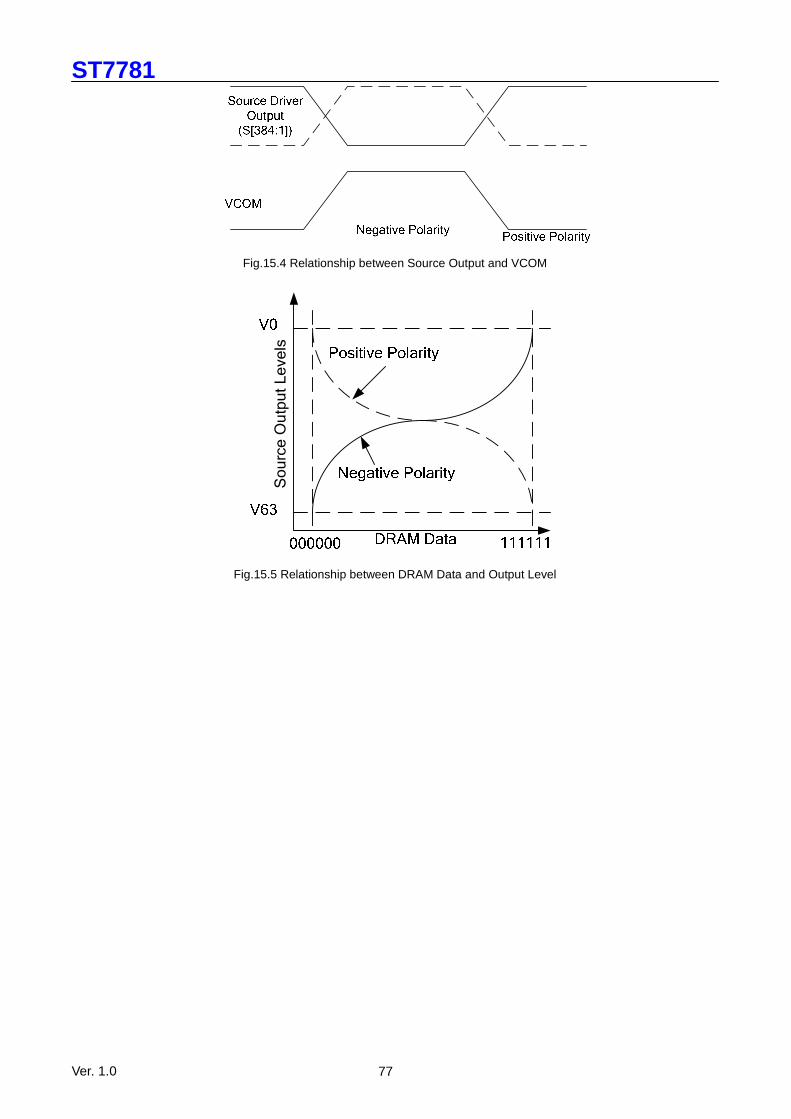
ST7781
Ver. 1.0 77
Fig.15.4 Relationship between Source Output and VCOM
Source Output Levels
Fig.15.5 Relationship between DRAM Data and Output Level
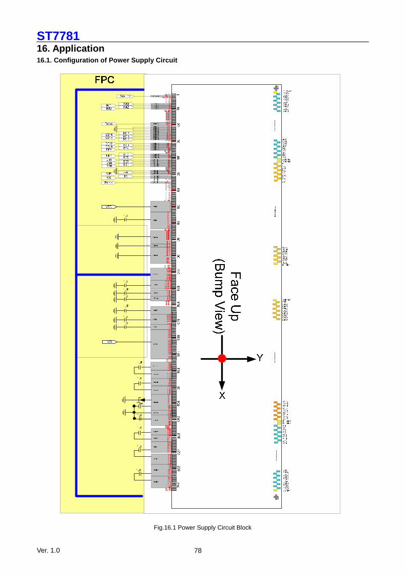
ST7781
Ver. 1.0 78
16. Application 16.1. Configuration of Power Supply Circuit
Fig.16.1 Power Supply Circuit Block
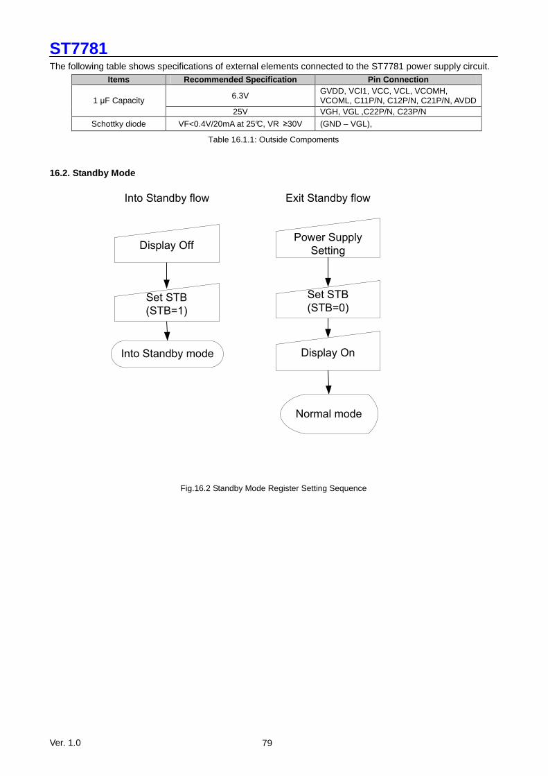
ST7781
Ver. 1.0 79
The following table shows specifications of external elements connected to the ST7781 power supply circuit. Items Recommended Specification Pin Connection
6.3V GVDD, VCI1, VCC, VCL, VCOMH, VCOML, C11P/N, C12P/N, C21P/N, AVDD 1 µF Capacity
25V VGH, VGL ,C22P/N, C23P/N
Schottky diode VF<0.4V/20mA at 25°C, VR ≥30V (GND – VGL),
Table 16.1.1: Outside Compoments
16.2. Standby Mode
Display Off
Set STB
(STB=1)
Display On
Set STB
(STB=0)
Into Standby mode
Into Standby flow
Power Supply
Setting
Exit Standby flow
Normal mode
Fig.16.2 Standby Mode Register Setting Sequence
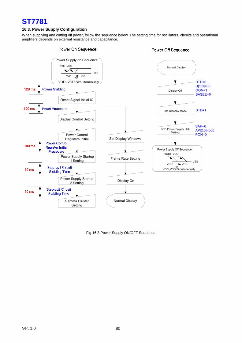
ST7781
Ver. 1.0 80
16.3. Power Supply Configuration When supplying and cutting off power, follow the sequence below. The setting time for oscillators, circuits and operational amplifiers depends on external resistance and capacitance.
SAP=0
AP[2:0]=000
PON=0
Power Supply Off Sequence
VSS
VDDI VDD
VDDI VDDor
VDDI,VDD Simultaneously
Normal Display
Display Off
DTE=0
D[1:0]=00
GON=1
BASEE=0
Into Standby Mode STB=1
LCD Power Supply Halt Setting
Power Supply on Sequence
VSS
VDDIVDD
VDDIVDD
Display Control Setting
Power Control
Registers Initial
Power Supply Startup
1 Setting
Power Supply Startup
2 Setting
Gamma Cluster
Setting
Set Display Windows
Normal Display
or
VDDI,VDD Simultaneously
Frame Rate Setting
Display On
Reset Signal Initial IC
Fig.16.3 Power Supply ON/OFF Sequence
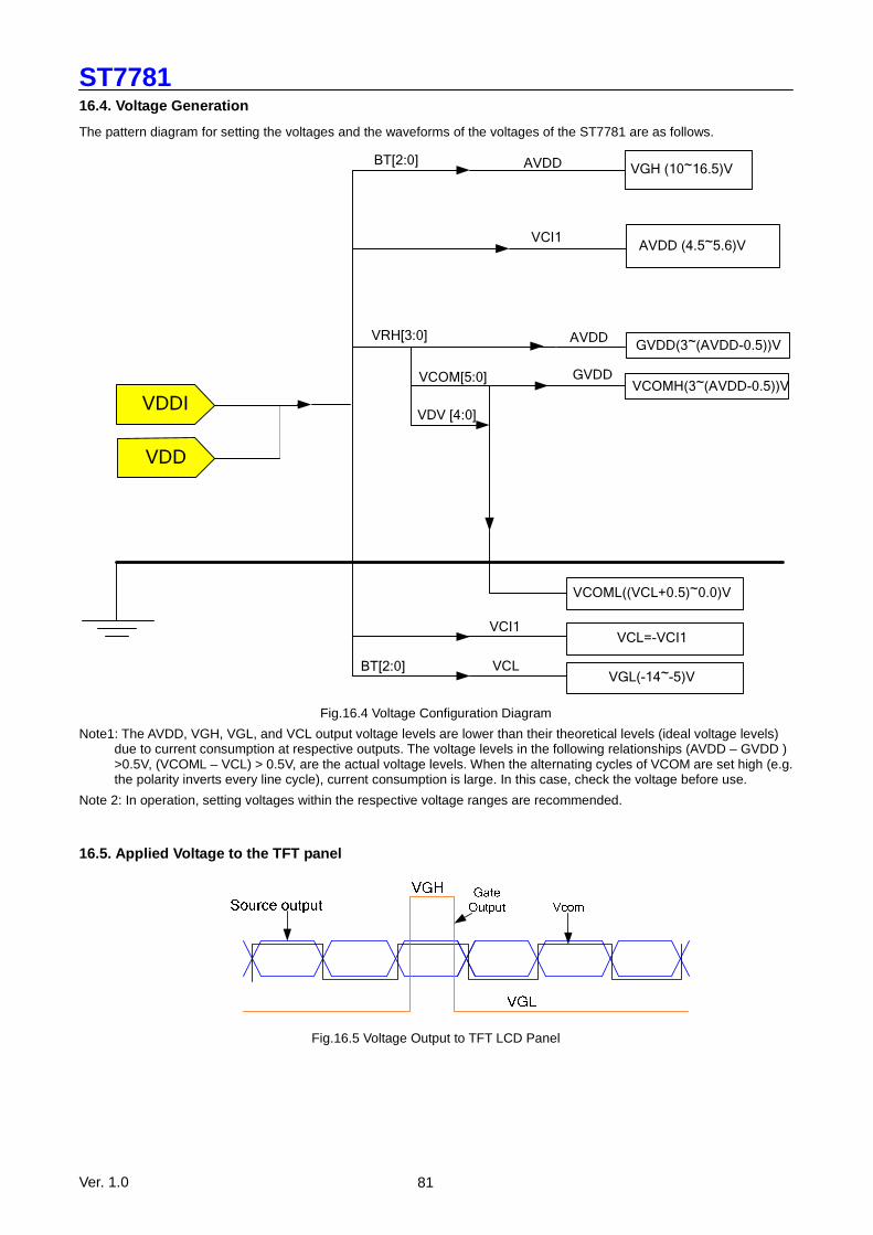
ST7781
Ver. 1.0 81
16.4. Voltage Generation
The pattern diagram for setting the voltages and the waveforms of the voltages of the ST7781 are as follows.
VDDI
BT[2:0]VGH (10~16.5)V
AVDD (4.5~5.6)V VCI1
VRH[3:0]
VDV [4:0]
VCOML((VCL+0.5)~0.0)V
AVDD
VCI1
VCL
VDD
GVDD(3~(AVDD-0.5))V
VCOMH(3~(AVDD-0.5))VGVDDVCOM[5:0]
VCL=-VCI1
VGL(-14~-5)VBT[2:0]
AVDD
Fig.16.4 Voltage Configuration Diagram
Note1: The AVDD, VGH, VGL, and VCL output voltage levels are lower than their theoretical levels (ideal voltage levels) due to current consumption at respective outputs. The voltage levels in the following relationships (AVDD – GVDD ) >0.5V, (VCOML – VCL) > 0.5V, are the actual voltage levels. When the alternating cycles of VCOM are set high (e.g. the polarity inverts every line cycle), current consumption is large. In this case, check the voltage before use.
Note 2: In operation, setting voltages within the respective voltage ranges are recommended.
16.5. Applied Voltage to the TFT panel
Fig.16.5 Voltage Output to TFT LCD Panel
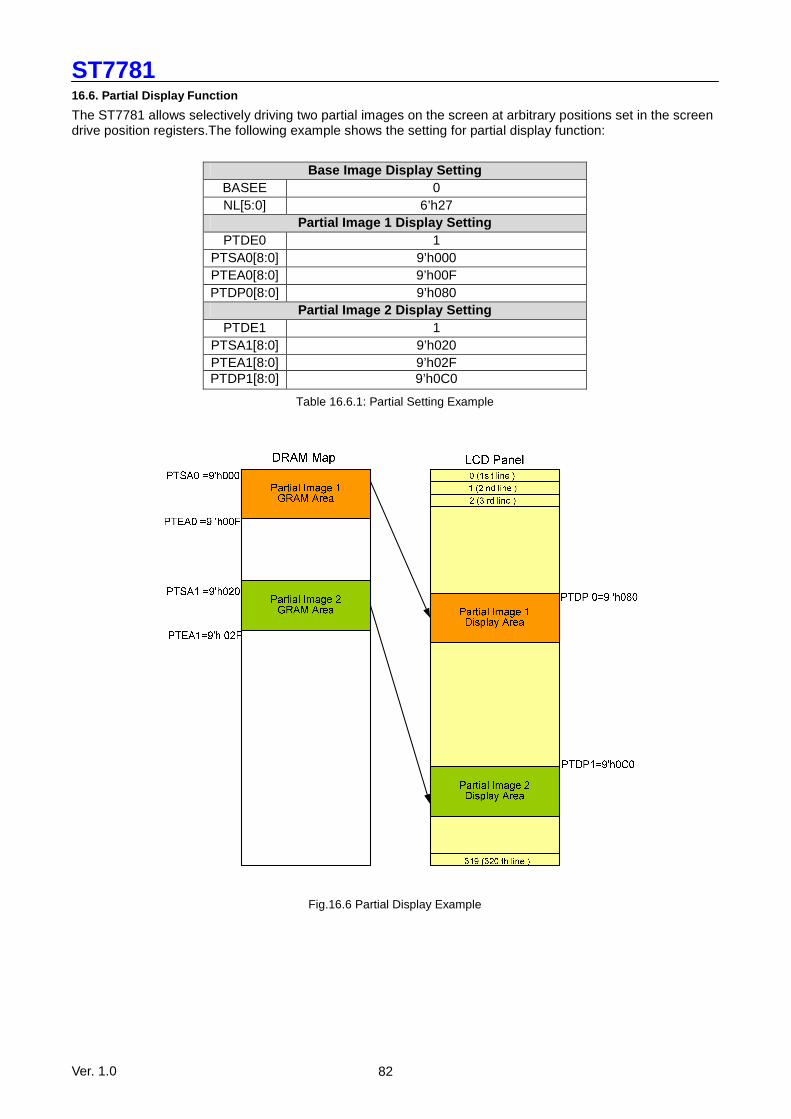
ST7781
Ver. 1.0 82
16.6. Partial Display Function
The ST7781 allows selectively driving two partial images on the screen at arbitrary positions set in the screen drive position registers.The following example shows the setting for partial display function:
Base Image Display Setting BASEE 0 NL[5:0] 6’h27
Partial Image 1 Display Setting PTDE0 1
PTSA0[8:0] 9’h000 PTEA0[8:0] 9’h00F PTDP0[8:0] 9’h080
Partial Image 2 Display Setting PTDE1 1
PTSA1[8:0] 9’h020 PTEA1[8:0] 9’h02F PTDP1[8:0] 9’h0C0
Table 16.6.1: Partial Setting Example
Fig.16.6 Partial Display Example
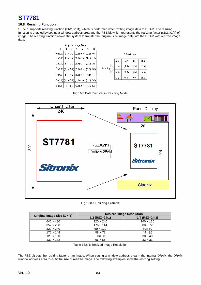
ST7781
Ver. 1.0 83
16.8. Resizing Function ST7781 supports resizing function (x1/2, x1/4), which is performed when writing image data to DRAM. The resizing function is enabled by setting a window address area and the RSZ bit which represents the resizing factor (x1/2, x1/4) of image. The resizing function allows the system to transfer the original-size image data into the DRAM with resized image data.
Fig.16.8 Data Transfer in Resizing Mode
320
160
Fig.16.8.1 Resizing Example
Resized Image Resolution Original Image Size (X × Y)
1/2 (RSZ=2’h1) 1/4 (RSZ=2’h3) 640 × 480 320 × 240 160 × 120 352 × 288 176 × 144 88 × 72 320 × 240 60 × 120 80× 60 176 × 144 88 × 72 44× 36 120 × 160 60× 80 30 × 40 132 × 132 66 × 66 33 × 33
Table 16.8.1: Resized Image Resolution
The RSZ bit sets the resizing factor of an image. When setting a window address area in the internal DRAM, the DRAM window address area must fit the size of resized image. The following examples show the resizing setting.
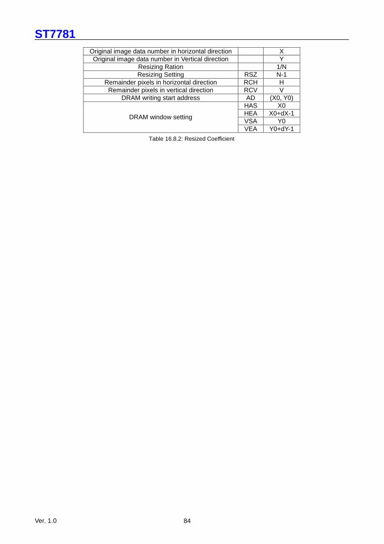
ST7781
Ver. 1.0 84
Original image data number in horizontal direction X Original image data number in Vertical direction Y
Resizing Ration 1/N Resizing Setting RSZ N-1
Remainder pixels in horizontal direction RCH H Remainder pixels in vertical direction RCV V
DRAM writing start address AD (X0, Y0) HAS X0 HEA X0+dX-1 VSA Y0
DRAM window setting
VEA Y0+dY-1
Table 16.8.2: Resized Coefficient
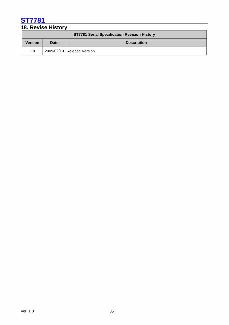
ST7781
Ver. 1.0 85
18. Revise History ST7781 Serial Specification Revision History
Version Date Description
1.0 2009/02/10 Release Version


![I n d e x [] · Ringhiera | Railing | Rampe | Barandilla | Oграждение Minimal Inox 304 | Minimal Stainless steel 304 | Minimal Inox 304 | Minimal Inox 304 | Minimal нержавеющая](https://static.fdocuments.net/doc/165x107/5ff0bd63ac95b9351f4a29e6/i-n-d-e-x-ringhiera-railing-rampe-barandilla-o-minimal.jpg)