Specifying and Measuring Nanometer Surface …. 93663a.p65(2 Specifying and Measuring Nanometer...
33
AEH. www.aehinc.com 93663a.p65(1 Specifying and Measuring Nanometer Surface Properties a seminar prepared for the American Society of Mechanical Engineers Alson E. Hatheway Alson E. Hatheway Inc. 787 West Woodbury Road Unit 10 Altadena, California 91001 v: (626)791-2243 f: (626)791-2194 e: [email protected]
Transcript of Specifying and Measuring Nanometer Surface …. 93663a.p65(2 Specifying and Measuring Nanometer...

AEH.www.aehinc.com
93663a.p65(1
Specifying and MeasuringNanometer Surface Properties
a seminar prepared for theAmerican Society of Mechanical Engineers
Alson E. Hatheway
Alson E. Hatheway Inc.787 West Woodbury Road
Unit 10Altadena, California 91001
v: (626)791-2243f: (626)791-2194

AEH.www.aehinc.com
93663a.p65(2
Specifying and MeasuringNanometer Surface Properties
1. Specifying and Measuring Nanometer Surface Properties - The 2002 edition ofASME B46.1 is the first national standard to address the specific issues associated withnanometer metrology. It has been eight years in the preparation.
2. ASME B46.1-2002 - Two new chapters are incorporated: Chapter 7 contains the nanom-eter metrology methods and Chapter 8 describes the performance limits of optical instru-ments often used in nanometer surface metrology. Accuracy was the principal concernof the committee since at the nanometer scale the metrology instruments are being usedat, or near, their limits of stability, sensitivity or both. To encourage accuracy the me-trologist is required to report the uncertainty of his measurements. He must also reportthe high and low limits to the passband. New calibration devices are incorporated in thestandard. Step heights have been included as a surface parameter, in part because theyare the preferred calibration devices (roughness calibration specimens are not recom-mended). Drift and curvature may be removed from the data. All contact and non-con-tact instruments are accommodated, including AFMs.

AEH.www.aehinc.com
93663a.p65(3
ASME B46.1-2002
New:Chapter 7 Nanometer Surface Texture and Step HeightsChapter 8 Optical Methods for Nanometer Surface Metrology
Accuracy, Accuracy, Accuracy
Measurement uncertainty to be reportedPassband reported
New calibration devicesStep height added as surface property
Drift and curvature may be removed from the dataAll contact and non-contact instruments, including AFMs

AEH.www.aehinc.com
93663a.p65(4
3. Accuracy - The accuracy issue is well illustrated by a nanometer-scale roughnessroundrobin sponsored by AMD in the mid-90s. The participants included nine industrialand academic metrology laboratories using all three of the most widely used atomicforce microscopes (AFMs). In a comparison of the laboratories’ measurements the high-est and lowest values varied by a factor of 8.5 for the peak-to-valley roughness and afactor of 6.8 for the root-mean-square roughness. There is clearly a major problem in thecalibration of the instruments. The five laboratories that have the best agreement stilldisagree by factors of 2.0 and 1.8.

AEH.www.aehinc.com
93663a.p65(5
Accuracy
Instruments from:Digital InstrumentsPark ScientificTopometrix
(After: Raheem, R., Advanced Micro Devices, Sunnyvale, California, 1996)
Participants:4 Semiconductor Manufacturers3 Instrument Makers1 University1 Independent Lab
8.5x 6.8x

AEH.www.aehinc.com
93663a.p65(6
4. Applications - The industries needing good nanometer metrology include;
a. Magnetic storage – The size of a written byte is controlled by the gap between therecording medium and the write head. The gap is maintained by the air that isdrawn between them and the aerodynamics of the air draft is controlled by theroughness on both the head and the medium. High density recording requiresclosely controlled surface roughness so the gap is neither too large nor too small.
b. Optical instruments – High performance optical instruments require very smoothsurfaces to suppress light scattering that limits the contrast of the image at the focalplane.
c. Semiconductors – Integrated circuits are requiring small features, line widths andfilm thickness. Since these are laid down in many overlaying layers very tight di-mensional tolerances are required on each step of the process. Semiconductors alsoneed a very smooth surface in the beginning.

AEH.www.aehinc.com
93663a.p65(7
Applications
Magnetic Disk Drives: head-to-disk air film controlled by roughness
Optical Instuments: low light scatter surfaces
Semiconductors: Thin films, shallow etches, small features and smooth surfaces
(Hutchinson Technology)
(G. M. Bennett, L. Mattsson)
(Digital Instruments)

AEH.www.aehinc.com
93663a.p65(8
5. Nanometer Metrology Instruments - Both contact and non-contact instruments areused in nanometer surface metrology. Ted Vorburger described the linear voltage differ-ential transformer (LVDT) often used in profiling instruments. The LVDT transducer isrelatively stable but near the limits of its sensitivity at the nanometer scale. AFMs derivetheir metrology from piezoelectric transducers that scan the specimen in three directions.The surface height is derived from the transducer voltage by driving the Z-axis trans-ducer to null the optical signal that is sensitive to the force on the tip of the probe. Thephase measuring interferometric microscope also derives its metrology from a piezoelec-tric transducer. The microscope is driven in the Z direction by the transducer and theheight of the surface is determined from the voltage on the transducer when the fringeappears. The piezoelectric transducer is relatively sensitive at the nanometer level but isunstable and requires frequent calibration.

AEH.www.aehinc.com
93663a.p65(9
Nanometer Metrology Instruments
Contact Types
(DigitalInstruments)
(Queensgate)
Non-contact Types
(D. Cohen)
(Wyco)

AEH.www.aehinc.com
93663a.p65(10
6. Instrument Responses (1) - The type of instrument used to make nanometer scale mea-surements may strongly affect the result. A stylus/probe instrument may be sensitive tomuch shorter wavelengths than an optical instrument. The difference may be nearly afactor of two in the indicated roughness. An LVDT transducer may also include morenoise because it is being used near the limits of its sensitivity.

AEH.www.aehinc.com
93663a.p65(11
Instrument Responses (1)
InterferometricProfiler
Stylus/ProbeProfiler
(After T. Vorburger, from J. M. Bennett et al.)

AEH.www.aehinc.com
93663a.p65(12
7. Instrument Responses (2) - The instability of a piezoelectric transducer in an AFM isshown in a train of 3.70 nanometer steps generated by a Hewlett-Packard signal genera-tor driving a calibrated displacement actuator. The steps were measured by an AFM.Three steps were selected for evaluation and their mean was about 14% high (4.22 na-nometers) and their standard deviation was about 10% of the step size. The mean valuemay be corrected by calibration at-size. The uncertainty of the size of the feature maythen be reduced by averaging more measurements.

AEH.www.aehinc.com
93663a.p65(13
Instrument Responses (2)
Nanoscope 5000
Train of 3.70 nm steps from theHECTORtm calibrated displacementactuator (0.0143 ampere from aHewlett-Packard waveform genera-tor).
ErrorMean (3) 2.937 nm -20.6%Std. Dev. (3) 0.252 nm 6.8%
HECTOR and HECTOR-100 are trademarks of Alson E. Hatheway Inc.
AEH.www.aehinc.com
93663a.p65(14
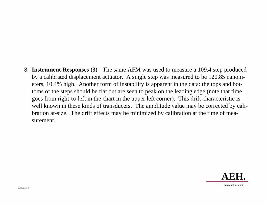
8. Instrument Responses (3) - The same AFM was used to measure a 109.4 step producedby a calibrated displacement actuator. A single step was measured to be 120.85 nanom-eters, 10.4% high. Another form of instability is apparent in the data: the tops and bot-toms of the steps should be flat but are seen to peak on the leading edge (note that timegoes from right-to-left in the chart in the upper left corner). This drift characteristic iswell known in these kinds of transducers. The amplitude value may be corrected by cali-bration at-size. The drift effects may be minimized by calibration at the time of mea-surement.

AEH.www.aehinc.com
93663a.p65(15
Instrument Responses (3)
Nanoscope 5000
Train of 109.4 nm steps from theHECTORtm calibrated displacementactuator
ErrorStep (1) 120.85 nm +10.5%
Instability visible in plateaus andfloors.

AEH.www.aehinc.com
93663a.p65(16
9. Nanometer Calibration Devices - Calibration for nanometer surface measurementsmust be performed with a known step height. Roughness calibration specimens are notrecommended. There are three calibration devices currently available: CalibrationSpecimens are available in height above about 8 nanometers and with an uncertainty ofabout 0.1 nanometers; Single Silicon Atom Steps are available at a step size of 0.31 na-nometers and an uncertainty of about 6.0%; Calibrated Displacement Actuators producesteps of any size between +100 and–100 (grooves) nanometers with an uncertainty of about 0.04%. Any calibration devicemust contain an estimate of its uncertainty.

AEH.www.aehinc.com
93663a.p65(17
Calibration Specimens8.0 nanometers and larger(U
k=2 = ~0.1 nm)
Single Silicon Atom Steps0.31 nanometers(U
k=2 = 6.0%)
Calibrated Displacement Actuators100 nanometers to 0.01 nanometer(U
k=2 = 0.04%)
Calibration device must include an evaluation of its uncertainty
Nanometer Calibration Devices
HECTOR-100
(T. Vorburger)
(A. E. Hatheway)
- 4
- 2
0
2
4
6
8
1 0
1 2
1 4
0 2 0 0 4 0 0 6 0 0 8 0 0 1 0 0 0 1 2 0 0 1 4 0 0
Hei
ght,
å

AEH.www.aehinc.com
93663a.p65(18
10. The Treatment of Uncertainty - The report of the measurement must contain a state-ment of the uncertainty of the reported value. Uncertainty is to be treated in accordancewith the ISO’s “Guide to the Expression of Uncertainty in Measurement.” Sources ofuncertainty to be considered include the irregularity of the feature being measured, in-strument stability and sensitivity limits, environmental influences and the calibrationdevice. All sources of uncertainty should be considered. The uncertainty of the mea-surement should be small with respect to the size of the feature being measured. A “cov-erage factor” of 2.0 is used to determine the “expanded uncertainty” that is reported.

AEH.www.aehinc.com
93663a.p65(19
The Treatment of UncertaintyUncertainty
standard uncertainty = u = standard deviation of a measurementexpanded uncertainty = U = ku
coverage factor = k = 2.0 for B46.1 reporting
Sources of Uncertainty in a MeasurementFeature irregularity
EnvironmentInstrument
Calibration device
Types of UncertaintyEvaluation by analysis, Type A
Evaluation by other methods, Type B
References: Guide to the Expression of Uncertainty in Measurementaka: “GUM”
Available from ISOMethods for Improving Accuracy of Measurements
ASME b46.1, Project Team 29

AEH.www.aehinc.com
93663a.p65(20
11. Annotations to the Report - Some data processing is permitted before calculating sur-face parameters but must be noted in the report. If zero point drift is removed the re-ported value must be followed by the word “Leveled.” If curvature or other form is re-moved the reported value must be followed by the phrase “Form removed.” If other dataprocessing procedures are used the reported value must be followed by the phrase “Otherthan GUM.” When non-analytical estimates of uncertainty are included the measure-ment uncertainty must be followed by the phrase “Included Type B components.”

AEH.www.aehinc.com
93663a.p65(21
Annotations to the Report
Zero Point Drift Correction...the measured value shall be followed by the phrase “Leveled.”
Curvature (Form) Removal...the measured value shall be followed by the phrase “Form removed.”
Other Data Processing Procedures...the measurment uncertainty shall be followed by the phrase “Other than GUM.”
Non-analytical Estimates of Uncertainty (GUM)...the measurement uncertainty shall be followed by the phrase
“includes Type B components.”

AEH.www.aehinc.com
93663a.p65(22
12. Specifying Nanometer Surface Roughness - A roughness specification may utilizethe symbology of ASME Y14.36 but the short wavelength cutoff must be placed in anote. The note must also call out ASME B46.1, Chapter 7, if the methods for nanometermetrology are desired. Note: ASME B46.1 does not distinguish a threshold at whichnanometer methodology is to be used, this must be determined by the engineer.

AEH.www.aehinc.com
93663a.p65(23
Specifying Nanometer Surface Roughness
0.005 1.2
The roughness, Ra, is a maximumvalue (0.005 micrometers).
The long-wavelength cutoff, λλλλλc, isshown (1.2 mm).
2
2 Measurement shall conform to ASMEB46.1, Chapter 7. The short-wavelengthcutoff, λs, shall be less than 0.8 microme-ter.

AEH.www.aehinc.com
93663a.p65(24
13. Nanometer Surface Roughness Reports - The report of the measurement of the sur-face parameter shows that the roughness is acceptable. The data were leveled (zero pointdrift was removed before calculating Ra) and the estimate of uncertainty included non-analytical components. The uncertainty was about 37.5% of the measured value.

AEH.www.aehinc.com
93663a.p65(25
Sample: AX55654-AThe Measured Property: RaThe Measured Value: 2.24 nm, LeveledThe Expanded Uncertainty (k=2) of the Measurement: .84 nm, includes
Type B componentsTransmission Band: 0.5 µm to 1200 µmDate and Time: Dec. 12, 1999, 455PMName of Metrologist: John Smith
Note: 2.24 + 0.84 = 3.08 nanometer < 0.005 micrometersThe Ra is acceptable
Nanometer Surface Roughness Reports

AEH.www.aehinc.com
93663a.p65(26
14. Specifying Nanometer Step Heights - A step height specification must be placed inthe notes and referenced at the appropriate location on the drawing (there is no standardsymbology for step heights). The note must call out ASME B46.1. Chapter 7 will beused since it is the only place step heights are measured in the standard. However, call-ing out Chapter 7 will reduce the possibility of using the wrong method.

AEH.www.aehinc.com
93663a.p65(27
Specifying Nanometer Step Heights
2 The thickness of the copper film shall be0.005 ±0.001 micrometers. It shall bemeasured as a step height, Zs, in accor-dance with ASME B46.1. The short-wavelength cutoff, λs, shall be less than0.8 micrometer. The long-wavelengthcutoff, λc, shall be 1.2 millimeters.
2

AEH.www.aehinc.com
93663a.p65(28
15. Nanometer Step Height Reports - The report of the measurement of the step heightshows it to be unacceptable.

AEH.www.aehinc.com
93663a.p65(29
Sample: AX55654-BThe Measured Property: ZsThe Measured Value: 2.24 nm, LeveledThe Expanded Uncertainty (k=2) of the Measurement: .84 nm, includes
Type B componentsTransmission Band: 0.5 µm to 1200 µmDate and Time: Dec. 12, 1999, 465PMName of Metrologist: John Smith
Note: 2.24 + 0.84 = 3.08 nanometer < 0.004 micrometersThe Zs is unacceptable
Nanometer Step Height Reports

AEH.www.aehinc.com
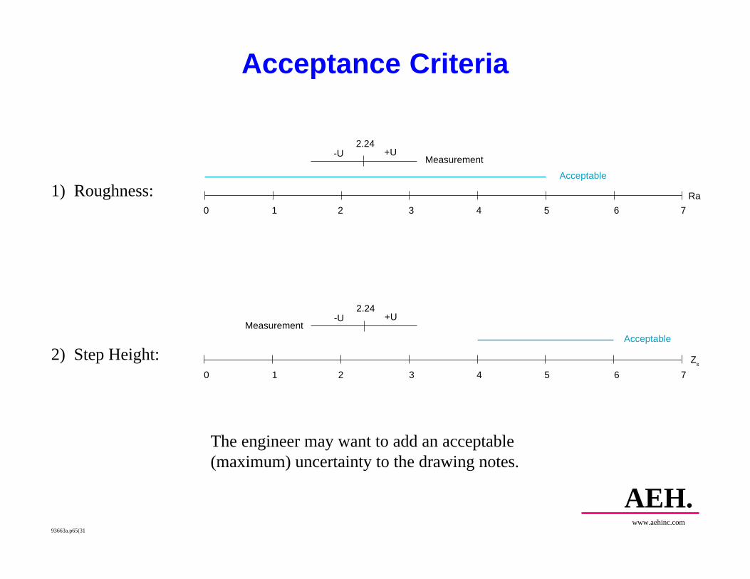
93663a.p65(30
16. Acceptance Criteria - The reporting of uncertainty provides the designer and engineerwith additional data about the quality of the measurements. Normal inspection willprobably ignore the uncertainty and use the conventional criteria for evaluation unlessanother policy is instituted by the organization. Designers and engineers may specify (inthe notes) the uncertainty associated with a measurement. Adjusting the tolerances maythen assure that accepted surface measurements fall within the acceptable range of val-ues.
AEH.www.aehinc.com
93663a.p65(31
Acceptance Criteria
1) Roughness:
2) Step Height:
0 1 2 3 4 5 6 7
0 1 2 3 4 5 6 7
Ra
Zs
2.24-U +U
Acceptable
Measurement
Acceptable
2.24-U +U
Measurement
The engineer may want to add an acceptable(maximum) uncertainty to the drawing notes.

AEH.www.aehinc.com
93663a.p65(32
17. ASME B46.1-2003 Nanometer Summary - Two new chapters have been incorpo-rated: Chapter 7 contains the nanometer metrology methods and Chapter 8 describes theperformance limits of optical instruments often used in nanometer surface metrology.Accuracy was the principal concern of the committee since at the nanometer scale themetrology instruments are being used at, or near, their limits of stability, sensitivity orboth. To encourage accuracy the metrologist is required to report the uncertainty of hismeasurements. He must also report the high and low limits to the passband. New cali-bration devices are incorporated in the standard. Step heights have been included as asurface parameter, in part because they are the preferred calibration devices (roughnesscalibration specimens are not recommended). Drift and curvature may be removed fromthe data. All contact and non-contact instruments are accommodated, including AFMs.

AEH.www.aehinc.com
93663a.p65(33
ASME B46.1-2002 Nanometer Summary
New:Chapter 7 Nanometer Surface Texture and Step HeightsChapter 8 Optical Methods for Nanometer Surface Metrology
Accuracy, Accuracy, Accuracy
Measurement uncertainty to be reportedPassband reported
New calibration devicesStep height added as surface property
Drift and curvature may be removed from the dataAll contact and non-contact instruments, including AFMs


![Time-resolved investigation of nanometer scale deformations ...lup.lub.lu.se/search/ws/files/3153570/2426299.pdfusing slope measuring deflectometry techniques [8], the in situ performance](https://static.fdocuments.net/doc/165x107/60b6f596e449d25168555c7b/time-resolved-investigation-of-nanometer-scale-deformations-luplublusesearchwsfiles3153570.jpg)