SPECIFICATIONS - Scancraft Display0).pdf · PG24064LRS-EGA-H-Q Rev.0(DK) Page3 Contents 1....
31
TECH. CORP. SPECIFICATIONS CUSTOMER : CIT006 ARROW SAMPLE CODE (Ver.) : PG24064LRS-EGA-H-Q (VER.0) MASS PRODUCTION CODE (Ver.) DRAWING NO. (Ver.) : PG-95010 Customer Approved Date: Approved QC Confirmed Designer ■ Approval For Specifications Only. * This specification is subject to change without notice. Please contact Powertip or it’s representative before designing your product based on this specification. □ Approval For Specifications and Sample. POWERTIP TECH. CORP. Headquarters: No.8, 6 th Road, Taichung Industrial Park, Taichung, Taiwan 台中市 407 工業區六路 8 號 TEL: 886-4-2355-8168 FAX: 886-4-2355-8166 E-mail: [email protected] Http://www.powertip.com.tw
Transcript of SPECIFICATIONS - Scancraft Display0).pdf · PG24064LRS-EGA-H-Q Rev.0(DK) Page3 Contents 1....

TECH. CORP.
SPECIFICATIONS
CUSTOMER : CIT006
ARROW
SAMPLE CODE (Ver.) :
PG24064LRS-EGA-H-Q (VER.0) MASS PRODUCTION CODE (Ver.) DRAWING NO. (Ver.)
: PG-95010
Customer Approved
Date:
Approved QC Confirmed Designer
Approval For Specifications Only.
* This specification is subject to change without notice.
Please contact Powertip or it’s representative before designing your product based on this specification.
Approval For Specifications and Sample.
POWERTIP TECH. CORP. Headquarters: No.8, 6th Road, Taichung Industrial Park,
Taichung, Taiwan
台中市 407工業區六路 8號
TEL: 886-4-2355-8168
FAX: 886-4-2355-8166
E-mail: [email protected]
Http://www.powertip.com.tw

PG24064LRS-EGA-H-Q Rev.0(DK) Page2
RECORDS OF REVISION
Date Rev. Description Note Page
2006/02/24 0 NEW SAMPLE
Total:34 Page

PG24064LRS-EGA-H-Q Rev.0(DK) Page3
Contents
1. SPECIFICATIONS 1.1 Features 1.2 Mechanical Specifications 1.3 Absolute Maximum Ratings 1.4 DC Electrical Characteristics 1.5 Optical Characteristics 1.6 Backlight Characteristics 2. MODULE STRUCTURE 2.1 Counter Drawing 2.2 Interface Pin Description 2.3 Timing Characteristics 2.4 Display Command 3. QUALITY ASSURANCE SYSTEM 3.1 Quality Assurance Flow Chart 3.2 Inspection Specification
4. RELIABILITY TEST 4.1 Reliability Test Condition
5. PRECAUTION RELATING PRODUCT HANDLING 5.1 Safety 5.2 Handling 5.3 Storage 5.4 Terms of Warranty
Note:For detailed information please refer to IC data sheet:T6963C,LC7940,LC7942

PG24064LRS-EGA-H-Q Rev.0(DK) Page4
1. SPECIFICATIONS
1.1 Features Item Standard Value
Display Type 240 * 64 dots
LCD Type STN, YG, Transflective, Positive, Extended Temp.
Driver Condition LCD Module :1/64 Duty , 1/6 Bias
Viewing Direction 6 O’clock
Backlight YG LED B/L
Weight 171 g
Interface -
Other -
1.2 Mechanical Specifications Item Standard Value Unit
Outline Dimension 180.0 (L)*65.0 (W)*13.8(max)(H) mm
Viewing Area 134.0(L) *40.4(W) mm
Active Area 127.16(L) *33.88(W) mm
Dot Size 0.49(L)*0.49(W) mm
Dot Pitch 0.53(L)*0.53(W) mm Note:For detailed information please refer to LCM drawing
1.3 Absolute Maximum Ratings Item Symbol Condition Min. Max. Unit
Power Supply Voltage VDD - -0.3 7.0 V
LCD Driver Supply Voltage VLCD - 5.3 25 V
Input Voltage VIN - -0.3 VDD+0.3 V
Operating Temperature TOP Excluded B/L -20 70
Storage Temperature TST Excluded B/L -30 80
Storage Humidity HD Ta<40 - 90 %RH

PG24064LRS-EGA-H-Q Rev.0(DK) Page5
1.4 DC Electrical Characteristics
VDD = 5.0 V ± 10%,VSS = 0V,Ta = 25
Item Symbol Condition Min. Type Max. Unit
Logic Supply Voltage VDD - 4.5 5.0 5.5 V
“H” Input Voltage VIH - VDD-2.2 - VDD V
“L” Input Voltage VIL - 0 - 0.8 V
“H” Output Voltage VOH Ioh=-0.4mA VDD-0.3 - VDD V
“L” Output Voltage VOL Ioh=0.4mA 0 - 0.3 V
Supply Current IDD VDD = 5.0 V fOSC=3.0MHz
- 10.5 - mA
-20°C - - -
25°C*1 - 10.8 - LCM Driver Voltage VOP
70°C - - -
V
Note: *1. THE VOP TEST POINT IS VDD – VO.
1.5 Optical Characteristics
LCD Panel:1/64Duty,1/9Bias,VLCD =12.7 V,Ta = 25
Item Symbol Conditions Min. Type Max. Reference
View Angle θ C>2.0, ∅ = 0° -45° - - Notes 1 & 2
Contrast Ratio C θ = 5°, ∅ = 0° 3 7 - Note 3
Response Time(rise) tr θ = 5°, ∅ = 0° - 150 ms - Note 4
Response Time(fall) tf θ = 5°, ∅ = 0° - 300 ms - Note 4

PG24064LRS-EGA-H-Q Rev.0(DK) Page6
Light (when reflected) z (θ=0°)
Note 1: Definition of angles θ and ∅ Note 2: Definition of viewing angles θ1 and θ2
θ1 θ2 viewing angle θ (∅ fixed)
Note : Optimum viewing angle with the
naked eye and viewing angle θ at
Cmax. Above are not always the same
Note 3: Definition of contrast C Note 4: Definition of response time
Brightness (reflection) of unselected dot (B2) C =
Brightness (reflection) of selected dot (B1)
ContrastNon-selected state
VLCD
-VLCD
0
tf
90%
tr
10%
Selected state Non-selected state
Time
0 Note: Measured with a transmissive LCD
operating voltage (v) panel which is displayed 1 cm2
VLCD : Operating voltage fFRM : Frame frequency
tr : Response time (rise) tf : Response time (fall)
(%)
Brightness
(reflection)
Brightness (reflection) of
selected dot
Brightness
(reflection) of
unselected dot
Cmax.
2.0
Sensor
LCD panel X(∅=90°)
Light (when transmitted )
X’
Z’
Y(∅=0°)
(θ=90°)
∅
Y’(∅=180°) θ
B2
B1

PG24064LRS-EGA-H-Q Rev.0(DK) Page7
1.6 Backlight Characteristics
LCD Module with LED Backlight
Maximum Ratings Item Symbol Conditions Min. Max. Unit
Forward Current IF Ta =25 - 1625 mA
Reverse Voltage VR Ta =25 - 8 V
Power Dissipation PO Ta =25 - 7.4 W
Operating Temperature TOP - -20 70
Storage Temperature TST - -40 80
Solder Temp. for 3 Second - - - 260
Electrical / Optical Characteristics
Ta =25
Item Symbol Conditions Min. Type Max. Unit
Forward Voltage VF IF= 650 mA - 4.2 4.6 V
Reverse Current IR VR= 8 V - - 0.2 mA
Average Brightness (with LCD)
IV IF= 650 mA - - - cd/m2
Wavelength λp IF= 650 mA 571 - 576 nm
Luminous Intensity (without LCD)
IV IF=650 mA
176 220 - cd/m2
Color Yellow-green
PG24064LRS-EGA-H-Q Rev.0(DK) Page8
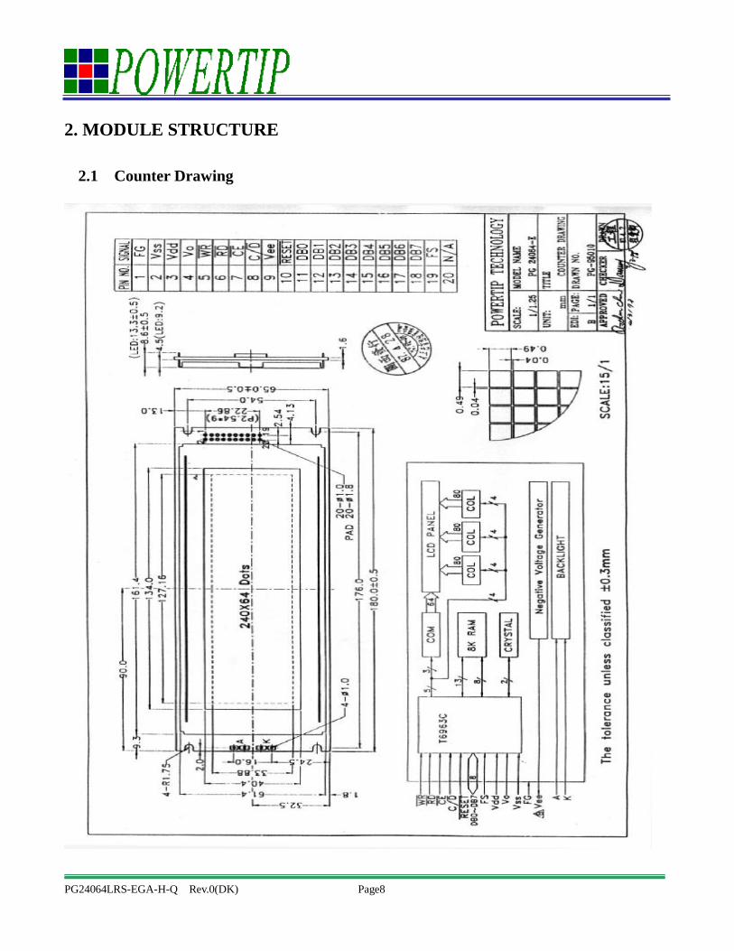
2. MODULE STRUCTURE
2.1 Counter Drawing

PG24064LRS-EGA-H-Q Rev.0(DK) Page9
2.2 Interface Pin Description
Pin No. Symbol Function 1 FG Frame ground (connected to metal bezel ) 2 VSS Power Supply (Vss=0) 3 VDD Power Supply (VDD>VSS) 4 VO Operating voltage for LCD
5 WR Data write (write data to the module at "L")
6 R D Data read (read data from the module at "L")
7 CE Chip enable for the module (active at "L")
8 C/ D WR ="L";C/ D = "H" :command write,C/ D ="L":data write
WR ="H";C/ D = "H" :command read, C/ D ="L":data read
9 VEE Negative voltage output
10 RESET Controller reset (module reset)
11~18 D0~D7 Data bus (D0=MSB, D7=LSB)
19 FS Font select :open or connect to VDD : 6*8 Dots font connect to VSS : 8*8 Dots font
20 NC Not connection Contrast Adjust
LCD MODULE
VDD 3
4
9
10~20KΩ
VO
VEE
4.2V
A K

PG24064LRS-EGA-H-Q Rev.0(DK) Page10
tDH
2.3 Timing Characteristics Bus Timing
C / D
tCDS
tCDH
CE
RD . WR tCE,
tRD,
tWR
tDS
D0~D7
(WRITE)
D0~D7
(READ)
tACC
tOH
Unless otherwise noted, VDD=5.0V±10%, VSS=0V, Ta=25
ITEM SYMBOL TEST CONDITION MIN. MAX. UNIT C/D Set Up Time tCDS - 100 - ns C/D Hold Time tCDH - 10 - ns
RD, WR Pulse Width tRD,tWR - 80 - ns Data Set Up Time tDS - 80 - ns Data Hold Time tDH - 40 - ns
Access Time tACC - - 150 ns Output Hold Time tOH - 10 50 ns
PG24064LRS-EGA-H-Q Rev.0(DK) Page11
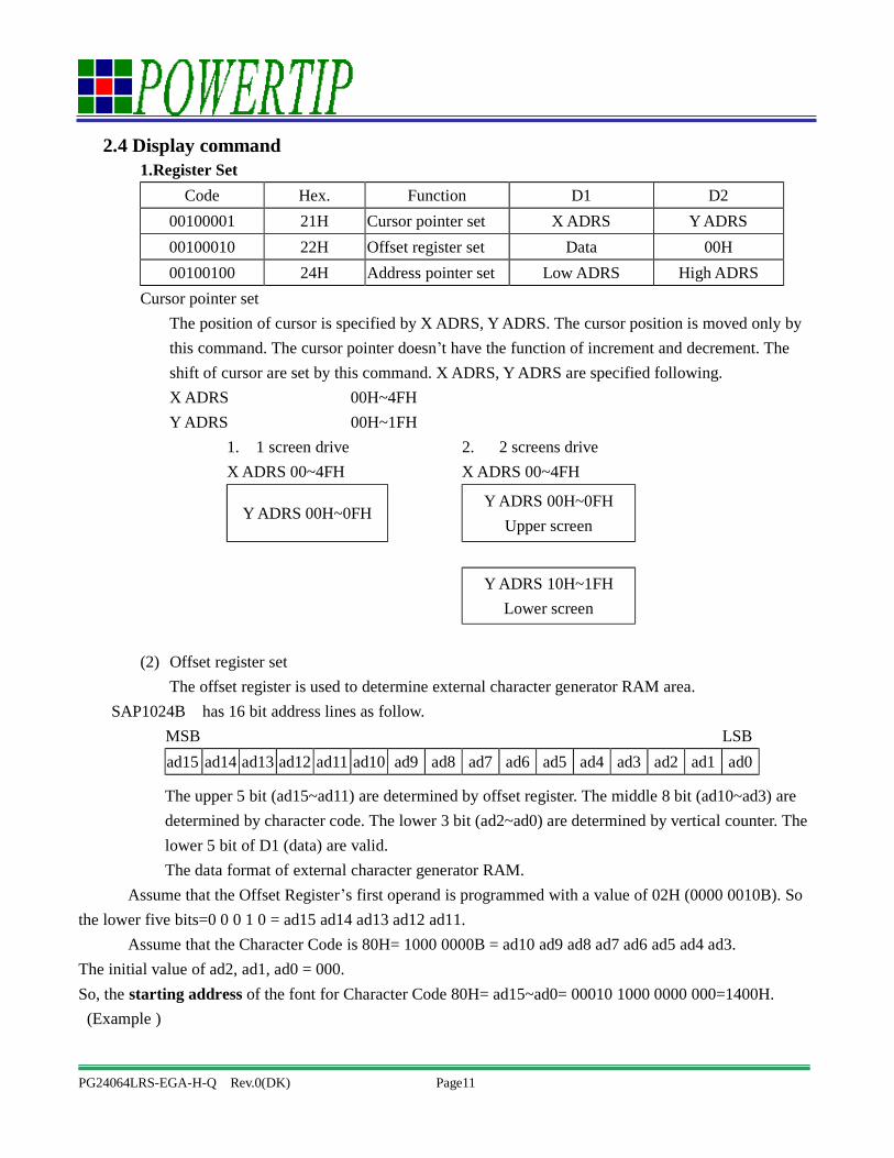
2.4 Display command 1.Register Set
Code Hex. Function D1 D2 00100001 21H Cursor pointer set X ADRS Y ADRS 00100010 22H Offset register set Data 00H 00100100 24H Address pointer set Low ADRS High ADRS
Cursor pointer set The position of cursor is specified by X ADRS, Y ADRS. The cursor position is moved only by
this command. The cursor pointer doesn’t have the function of increment and decrement. The shift of cursor are set by this command. X ADRS, Y ADRS are specified following.
X ADRS 00H~4FH Y ADRS 00H~1FH
1. 1 screen drive 2. 2 screens drive X ADRS 00~4FH X ADRS 00~4FH
Y ADRS 00H~0FH Y ADRS 00H~0FH
Upper screen
Y ADRS 10H~1FH
Lower screen
(2) Offset register set The offset register is used to determine external character generator RAM area.
SAP1024B has 16 bit address lines as follow. MSB LSB
ad15 ad14 ad13 ad12 ad11 ad10 ad9 ad8 ad7 ad6 ad5 ad4 ad3 ad2 ad1 ad0
The upper 5 bit (ad15~ad11) are determined by offset register. The middle 8 bit (ad10~ad3) are determined by character code. The lower 3 bit (ad2~ad0) are determined by vertical counter. The lower 5 bit of D1 (data) are valid. The data format of external character generator RAM.
Assume that the Offset Register’s first operand is programmed with a value of 02H (0000 0010B). So the lower five bits=0 0 0 1 0 = ad15 ad14 ad13 ad12 ad11.
Assume that the Character Code is 80H= 1000 0000B = ad10 ad9 ad8 ad7 ad6 ad5 ad4 ad3. The initial value of ad2, ad1, ad0 = 000. So, the starting address of the font for Character Code 80H= ad15~ad0= 00010 1000 0000 000=1400H. (Example )
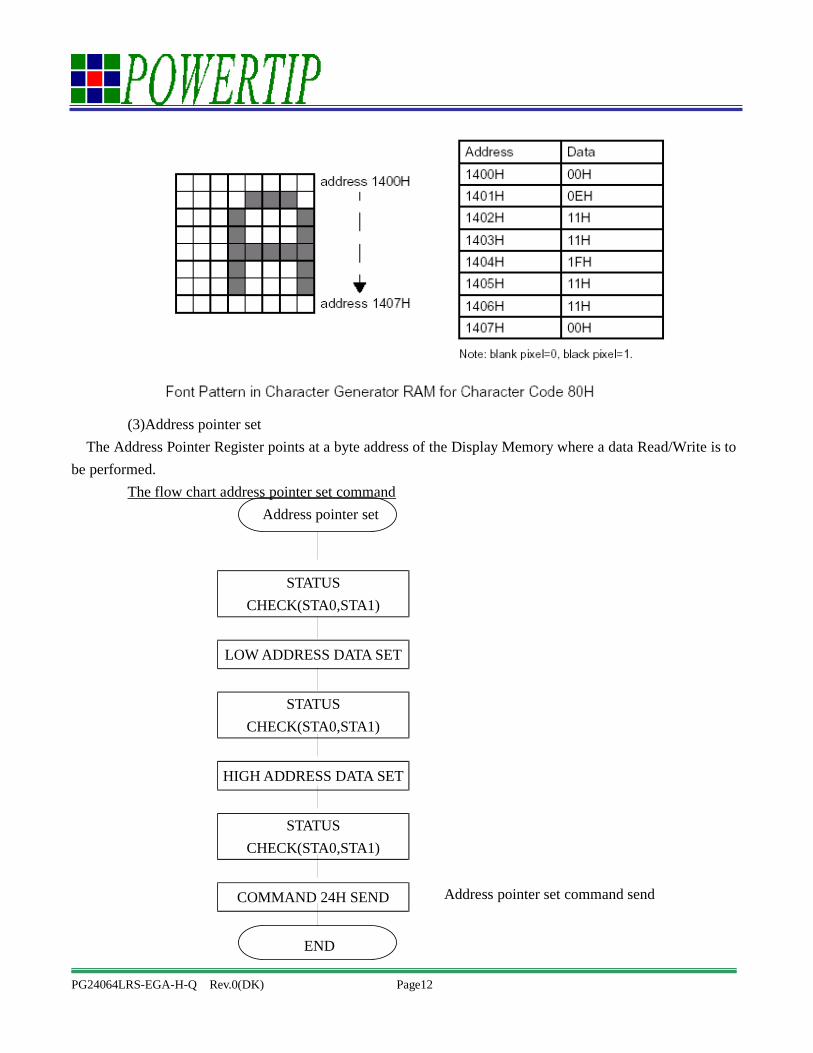
PG24064LRS-EGA-H-Q Rev.0(DK) Page12
(3)Address pointer set The Address Pointer Register points at a byte address of the Display Memory where a data Read/Write is to
be performed. The flow chart address pointer set command Address pointer set
STATUS CHECK(STA0,STA1)
LOW ADDRESS DATA SET
STATUS
CHECK(STA0,STA1)
HIGH ADDRESS DATA SET
STATUS
CHECK(STA0,STA1)
COMMAND 24H SEND
END
Address pointer set command send

PG24064LRS-EGA-H-Q Rev.0(DK) Page13
2.Control word set Four registers, Text Home Address Register, Text Area Register, Graphic Home Address Register, and Graphic Area Register, need to be programmed to define text display and graphic display.
Code Hex. Function D1 D2 0100 0000 40H Text home address set Low address High address 0100 0001 41H Text area set Columns 00H 0100 0010 42H Graphic home address set Low address High address 0100 0011 43H Graphic area set Columns 00H
(1) Text home address set The starting address of external display RAM for Text display is defined by this command. The text home address shows the left-most and top-most position.
the relation between Display Memory address and the display position
TH : Content of Text Home Address Register. TA : Content of Text Area Register.
CL : Column number, selected by setting the MD2 pin and the MD3 pin.
(Example) Content of Text Home Address Register. : 0000H Content of Text Area Register : 0020H MD2=H, MD3=H : 32 columns DUAL=H, MDS=L, MD0=L,MD1=H : 4 lines
0000H 0001H ---------- 001EH 001FH 0020H 0021H ----------- 003EH 003FH 0040H 0041H ----------- 005EH 005FH 0060H 0061H ----------- 007EH 007FH
(2)Graphic home address set The starting address of external display RAM for Graphic display is defined by this command. The Graphic home address show the left-most and top-most position
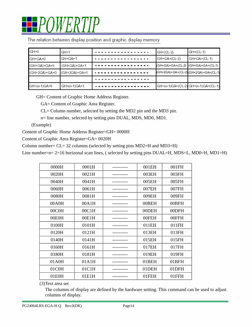
PG24064LRS-EGA-H-Q Rev.0(DK) Page14
GH= Content of Graphic Home Address Register. GA= Content of Graphic Area Register. CL= Column number, selected by setting the MD2 pin and the MD3 pin. n= line number, selected by setting pins DUAL, MDS, MD0, MD1.
(Example) Content of Graphic Home Address Register=GH= 0000H Content of Graphic Area Register=GA= 0020H Column number= CL= 32 columns (selected by setting pins MD2=H and MD3=H) Line number=n= 2=16 horizonal scan lines, ( selected by setting pins DUAL=H, MDS=L, MD0=H, MD1=H)
0000H 0001H ---------- 001EH 001FH 0020H 0021H ---------- 003EH 003FH 0040H 0041H ---------- 005EH 005FH 0060H 0061H ---------- 007EH 007FH 0080H 0081H ---------- 009EH 009FH 00A0H 00A1H ---------- 00BEH 00BFH 00C0H 00C1H ---------- 00DEH 00DFH 00E0H 00E1H ---------- 00FEH 00FFH 0100H 0101H ---------- 011EH 011FH 0120H 0121H ---------- 013EH 013FH 0140H 0141H ---------- 015EH 015FH 0160H 0161H ---------- 017EH 017FH 0180H 0181H ---------- 019EH 019FH 01A0H 01A1H ---------- 01BEH 01BFH 01C0H 01C1H ---------- 01DEH 01DFH 01E0H 01E1H ---------- 01FEH 01FFH
(3) Text area set The columns of display are defined by the hardware setting. This command can be used to adjust
columns of display.
PG24064LRS-EGA-H-Q Rev.0(DK) Page15
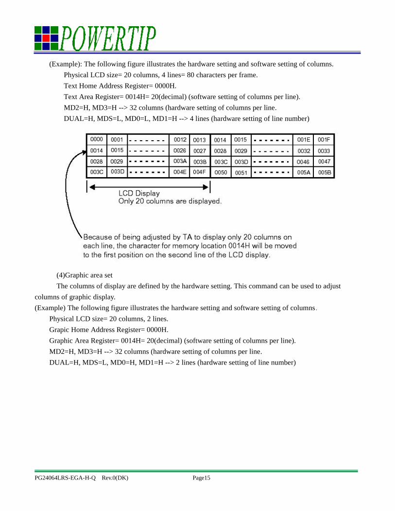
(Example): The following figure illustrates the hardware setting and software setting of columns. Physical LCD size= 20 columns, 4 lines= 80 characters per frame.
Text Home Address Register= 0000H. Text Area Register= 0014H= 20(decimal) (software setting of columns per line). MD2=H, MD3=H --> 32 columns (hardware setting of columns per line. DUAL=H, MDS=L, MD0=L, MD1=H --> 4 lines (hardware setting of line number)
(4)Graphic area set The columns of display are defined by the hardware setting. This command can be used to adjust
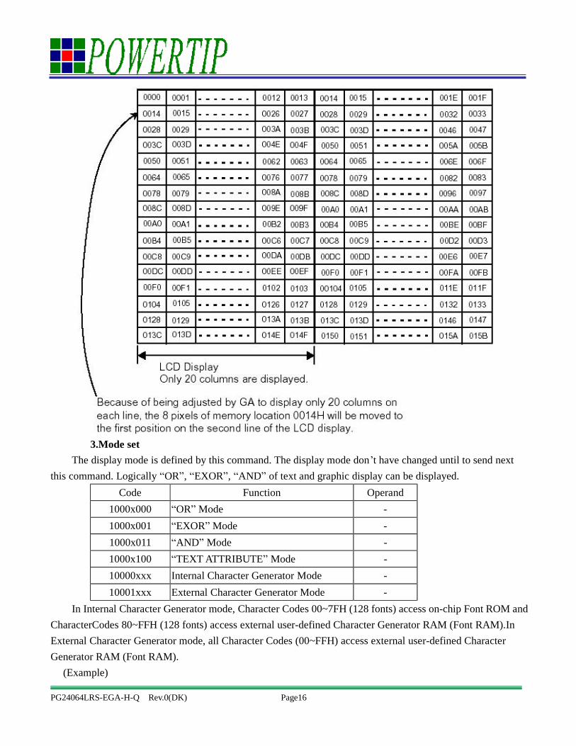
columns of graphic display. (Example) The following figure illustrates the hardware setting and software setting of columns .
Physical LCD size= 20 columns, 2 lines. Grapic Home Address Register= 0000H. Graphic Area Register= 0014H= 20(decimal) (software setting of columns per line). MD2=H, MD3=H --> 32 columns (hardware setting of columns per line. DUAL=H, MDS=L, MD0=H, MD1=H --> 2 lines (hardware setting of line number)
PG24064LRS-EGA-H-Q Rev.0(DK) Page16
3.Mode set
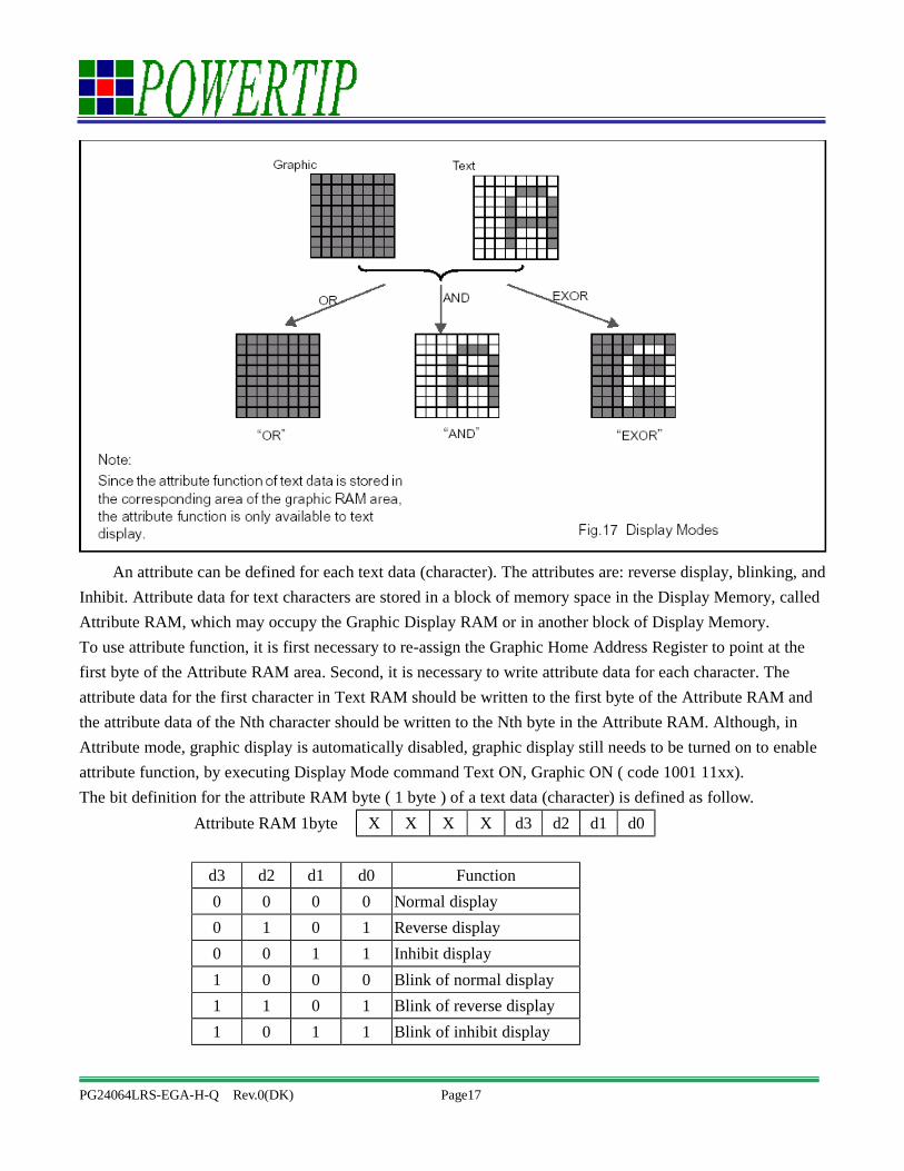
The display mode is defined by this command. The display mode don’t have changed until to send next this command. Logically “OR”, “EXOR”, “AND” of text and graphic display can be displayed.
Code Function Operand 1000x000 “OR” Mode - 1000x001 “EXOR” Mode - 1000x011 “AND” Mode - 1000x100 “TEXT ATTRIBUTE” Mode - 10000xxx Internal Character Generator Mode - 10001xxx External Character Generator Mode -
In Internal Character Generator mode, Character Codes 00~7FH (128 fonts) access on-chip Font ROM and CharacterCodes 80~FFH (128 fonts) access external user-defined Character Generator RAM (Font RAM).In External Character Generator mode, all Character Codes (00~FFH) access external user-defined Character Generator RAM (Font RAM). (Example)
PG24064LRS-EGA-H-Q Rev.0(DK) Page17
An attribute can be defined for each text data (character). The attributes are: reverse display, blinking, and Inhibit. Attribute data for text characters are stored in a block of memory space in the Display Memory, called Attribute RAM, which may occupy the Graphic Display RAM or in another block of Display Memory. To use attribute function, it is first necessary to re-assign the Graphic Home Address Register to point at the first byte of the Attribute RAM area. Second, it is necessary to write attribute data for each character. The attribute data for the first character in Text RAM should be written to the first byte of the Attribute RAM and the attribute data of the Nth character should be written to the Nth byte in the Attribute RAM. Although, in Attribute mode, graphic display is automatically disabled, graphic display still needs to be turned on to enable attribute function, by executing Display Mode command Text ON, Graphic ON ( code 1001 11xx). The bit definition for the attribute RAM byte ( 1 byte ) of a text data (character) is defined as follow.
Attribute RAM 1byte X X X X d3 d2 d1 d0
d3 d2 d1 d0 Function 0 0 0 0 Normal display 0 1 0 1 Reverse display 0 0 1 1 Inhibit display 1 0 0 0 Blink of normal display 1 1 0 1 Blink of reverse display 1 0 1 1 Blink of inhibit display
PG24064LRS-EGA-H-Q Rev.0(DK) Page18
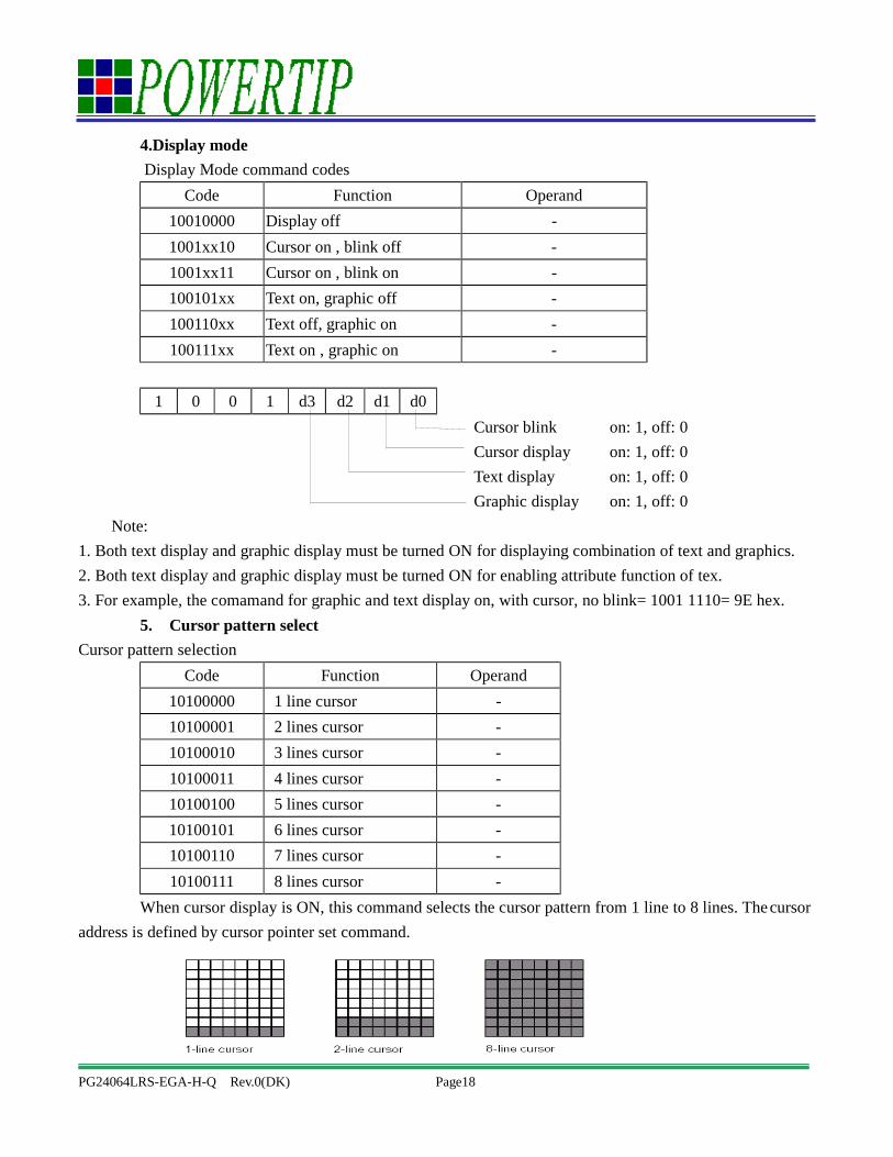
4.Display mode Display Mode command codes
Code Function Operand 10010000 Display off - 1001xx10 Cursor on , blink off - 1001xx11 Cursor on , blink on - 100101xx Text on, graphic off - 100110xx Text off, graphic on - 100111xx Text on , graphic on -
1 0 0 1 d3 d2 d1 d0
Cursor blink on: 1, off: 0 Cursor display on: 1, off: 0 Text display on: 1, off: 0 Graphic display on: 1, off: 0 Note: 1. Both text display and graphic display must be turned ON for displaying combination of text and graphics. 2. Both text display and graphic display must be turned ON for enabling attribute function of tex. 3. For example, the comamand for graphic and text display on, with cursor, no blink= 1001 1110= 9E hex.
5. Cursor pattern select Cursor pattern selection
Code Function Operand 10100000 1 line cursor - 10100001 2 lines cursor - 10100010 3 lines cursor - 10100011 4 lines cursor - 10100100 5 lines cursor - 10100101 6 lines cursor - 10100110 7 lines cursor - 10100111 8 lines cursor -
When cursor display is ON, this command selects the cursor pattern from 1 line to 8 lines. The cursor address is defined by cursor pointer set command.

PG24064LRS-EGA-H-Q Rev.0(DK) Page19
6.Data auto read/write Data Auto Read/Write commands.
Code Hex. Function Operand 10110000 B0H Data auto write set - 10110001 B1H Data auto read set - 10110010 B2H Terminate auto write read -
Data Auto Read, Data Auto Write, and Auto Mode Reset commands are single-byte commands. Auto Read/Write commands are useful for transferring a block of data to or from the Display Memory. After sending a Data Auto Read or Data Auto Write command, it is not necessary to send Data Read or Data Write command for each data byte transfer to or from the Display Memory. Address Pointer Register should be programmed to point at the initial byte address in the Display Memory. The Address Pointer Register will be automatically incremented by one after each Data Read/Data Write. After finishing the data transfer, a Auto Mode Reset command should be issued to terminate Auto Read/Write mode.
PG24064LRS-EGA-H-Q Rev.0(DK) Page20
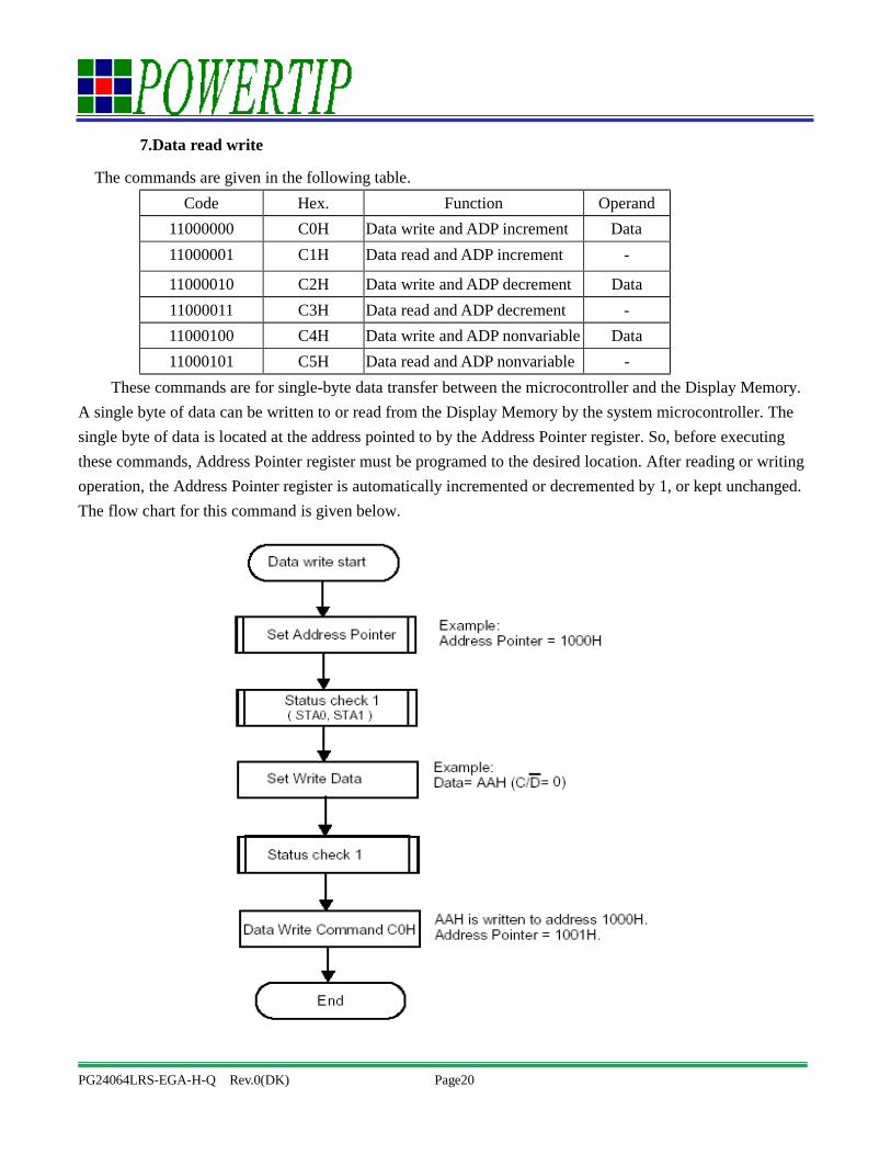
7.Data read write
The commands are given in the following table. Code Hex. Function Operand
11000000 C0H Data write and ADP increment Data 11000001 C1H Data read and ADP increment -
11000010 C2H Data write and ADP decrement Data 11000011 C3H Data read and ADP decrement - 11000100 C4H Data write and ADP nonvariable Data 11000101 C5H Data read and ADP nonvariable -
These commands are for single-byte data transfer between the microcontroller and the Display Memory. A single byte of data can be written to or read from the Display Memory by the system microcontroller. The single byte of data is located at the address pointed to by the Address Pointer register. So, before executing these commands, Address Pointer register must be programed to the desired location. After reading or writing operation, the Address Pointer register is automatically incremented or decremented by 1, or kept unchanged. The flow chart for this command is given below.

PG24064LRS-EGA-H-Q Rev.0(DK) Page21
NO
8.Screen peek
Code Hex. Function Operand 11100000 E0H screen peek -
The code for this command is 1110 0000 (E0 Hex). It is used to transfer 1 byte of displayed data to the data bus. This byte of data can then be read by the host microcontroller. The logical combination of text and graphic display data on the LCD screen can be read by this command. The status (STA6) should be checked just after “Screen peek” command. If the address determined by “Address pointer set” command is not in graphic area, this command ignored and status flag (STA6) is set. Please refer following flow chart. SCREEN PEEK START
STATUS CHECK 1
LOWER ADDRESS DATA
STATUS CHECK 1
UPPER ADDRESS DATA
STATUS CHECK 1
ADDRESS POINTER SET 24H
STATUS CHECK 1
SCREEN PEEK E0H STATUS CHECK STA6 =0 ? YES
STATUS CHECK 1
DATA ACCESS END

PG24064LRS-EGA-H-Q Rev.0(DK) Page22
9.Screen copy
Code Hex. Function Operand 11101000 E8H screen copy -
This command copies a single raster scan line of data to the graphic area. The starting address must be set using the Set Address Pointer command.
When Attribute Function is enabled, this command is not available, because the graphic area is used for storing attribute function of the text data.
Because the SAP1024B can not separate the upper screen data from the lower screen data, this command can not be used in dual-scan mode. Please refer following flow chart.
.

PG24064LRS-EGA-H-Q Rev.0(DK) Page23
10.Bit set/reset
Code Function Operand 11110xxx bit reset - 11111xxx bit set - 1111x000 bit 0 - 1111x001 bit 1 - 1111x010 bit 2 - 1111x011 bit 3 - 1111x100 bit 4 - 1111x101 bit 5 - 1111x110 bit 6 - 1111x111 bit 7 -
This command is used to set or reset an individual bit in the Display Memory. The byte address of the bit is pointed at by the Address Pointer register. This is a one-byte command.
PG24064LRS-EGA-H-Q Rev.0(DK) Page24
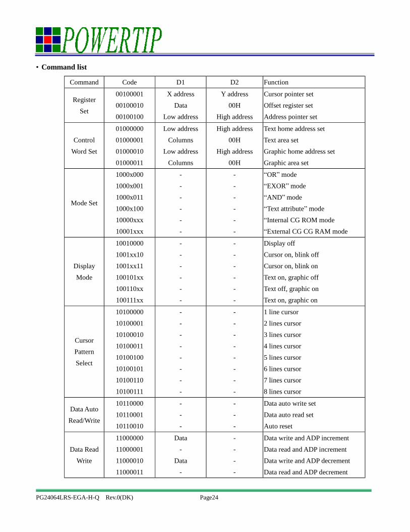
• Command list
Command Code D1 D2 Function
Register Set
00100001 00100010 00100100
X address Data
Low address
Y address 00H
High address
Cursor pointer set Offset register set Address pointer set
Control Word Set
01000000 01000001 01000010 01000011
Low address Columns
Low address Columns
High address 00H
High address 00H
Text home address set Text area set Graphic home address set Graphic area set
Mode Set
1000x000 1000x001 1000x011 1000x100 10000xxx 10001xxx
- - - - - -
- - - - - -
“OR” mode “EXOR” mode “AND” mode “Text attribute” mode “Internal CG ROM mode “External CG CG RAM mode
Display Mode
10010000 1001xx10 1001xx11 100101xx 100110xx 100111xx
- - - - - -
- - - - - -
Display off Cursor on, blink off Cursor on, blink on Text on, graphic off Text off, graphic on Text on, graphic on
Cursor Pattern Select
10100000 10100001 10100010 10100011 10100100 10100101 10100110 10100111
- - - - - - - -
- - - - - - - -
1 line cursor 2 lines cursor 3 lines cursor 4 lines cursor 5 lines cursor 6 lines cursor 7 lines cursor 8 lines cursor
Data Auto Read/Write
10110000 10110001 10110010
- - -
- - -
Data auto write set Data auto read set Auto reset
Data Read Write
11000000 11000001 11000010 11000011
Data -
Data -
- - - -
Data write and ADP increment Data read and ADP increment Data write and ADP decrement Data read and ADP decrement
PG24064LRS-EGA-H-Q Rev.0(DK) Page25
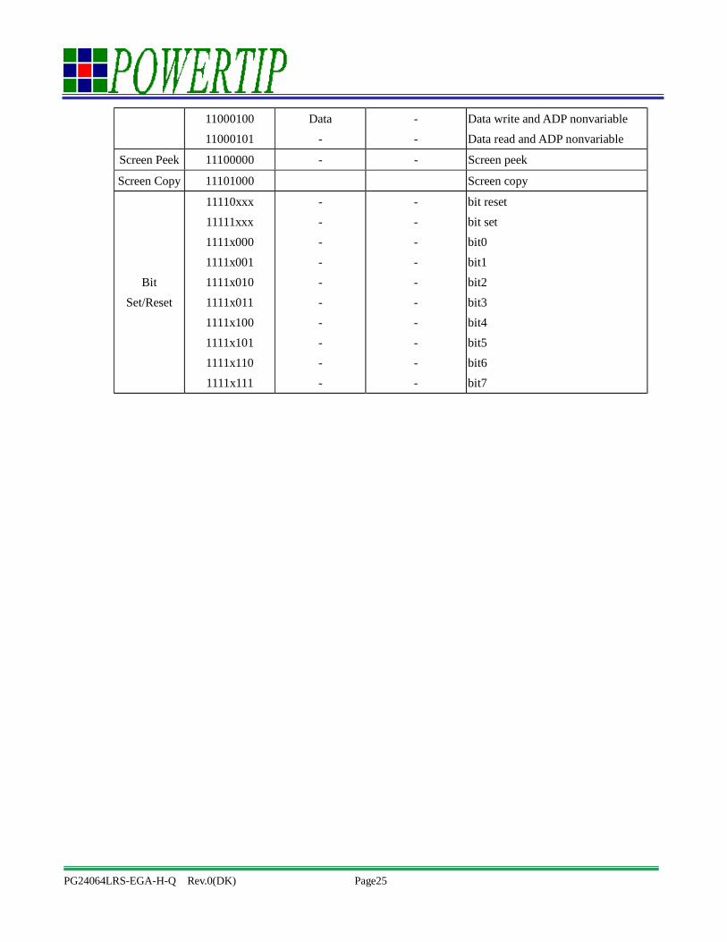
11000100 11000101
Data -
- -
Data write and ADP nonvariable Data read and ADP nonvariable
Screen Peek 11100000 - - Screen peek
Screen Copy 11101000 Screen copy
Bit Set/Reset
11110xxx 11111xxx 1111x000 1111x001 1111x010 1111x011 1111x100 1111x101 1111x110 1111x111
- - - - - - - - - -
- - - - - - - - - -
bit reset bit set bit0 bit1 bit2 bit3 bit4 bit5 bit6 bit7

PG24064LRS-EGA-H-Q Rev.0(DK) Page26
3. QUALITY ASSURANCE SYSTEM
3.1 Quality Assurance Flow Chart
Item Customer Sales R&D Q.A Manufactur
ing Product control
Purchase Inventory
control
Marketing &
Design
Sample Approval
Pilot Run &
Mass Product
Ship Out
OK
Request
Info Survey
Inquiry Project evaluation
Project Validation
Quote OK NG
Contract
Design check
Sample test
Verification
Sample approval
NG
NG
Pilot run & Reliability test
Verification
Specification preparation OK
Mass production
Inspection NG OK
Shipment
NG
Ship out
OK

PG24064LRS-EGA-H-Q Rev.0(DK) Page27
Item Customer Sales R&D Q.A Manufactu
ring Product control
Purchase Inventory
control
Sales Service
Q.A Activity
1. ISO 9001 Maintenance Activities 2. Process improvement proposal 3. Equipment calibration 4. Education And Training Activities 5. Standardization Management
Info Claim
Failure analysis
Corrective action
Tracking
Analysis report
PG24064LRS-EGA-H-Q Rev.0(DK) Page28
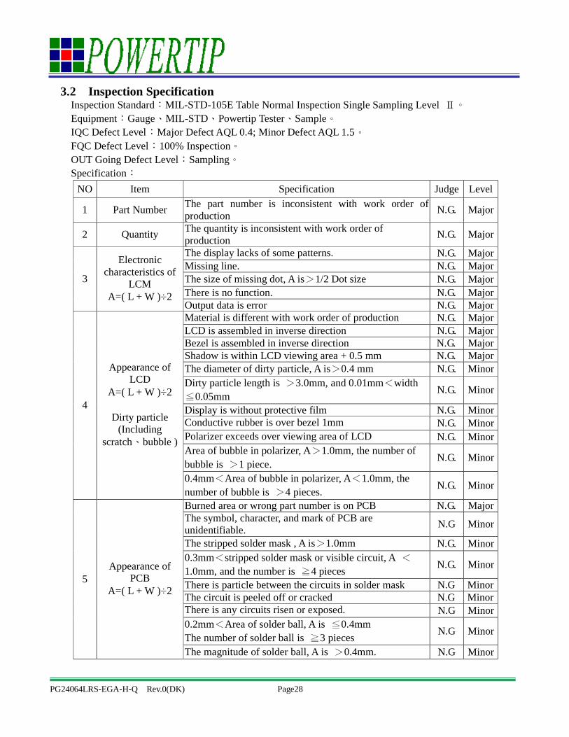
3.2 Inspection Specification Inspection Standard:MIL-STD-105E Table Normal Inspection Single Sampling Level Ⅱ。 Equipment:Gauge、MIL-STD、Powertip Tester、Sample。 IQC Defect Level:Major Defect AQL 0.4; Minor Defect AQL 1.5。 FQC Defect Level:100% Inspection。 OUT Going Defect Level:Sampling。 Specification:
NO Item Specification Judge Level
1 Part Number The part number is inconsistent with work order of production N.G. Major
2 Quantity The quantity is inconsistent with work order of production N.G. Major
The display lacks of some patterns. N.G. Major Missing line. N.G. Major The size of missing dot, A is>1/2 Dot size N.G. Major There is no function. N.G. Major
3
Electronic characteristics of
LCM A=( L + W )÷2
Output data is error N.G. Major Material is different with work order of production N.G. Major LCD is assembled in inverse direction N.G. Major Bezel is assembled in inverse direction N.G. Major Shadow is within LCD viewing area + 0.5 mm N.G. Major The diameter of dirty particle, A is>0.4 mm N.G. Minor Dirty particle length is >3.0mm, and 0.01mm<width ≦0.05mm N.G. Minor
Display is without protective film N.G. Minor Conductive rubber is over bezel 1mm N.G. Minor Polarizer exceeds over viewing area of LCD N.G. Minor Area of bubble in polarizer, A>1.0mm, the number of bubble is >1 piece. N.G. Minor
4
Appearance of LCD
A=( L + W )÷2
Dirty particle (Including
scratch、bubble )
0.4mm<Area of bubble in polarizer, A<1.0mm, the number of bubble is >4 pieces. N.G. Minor
Burned area or wrong part number is on PCB N.G. Major The symbol, character, and mark of PCB are unidentifiable. N.G Minor
The stripped solder mask , A is>1.0mm N.G. Minor 0.3mm<stripped solder mask or visible circuit, A <1.0mm, and the number is ≧4 pieces N.G. Minor
There is particle between the circuits in solder mask N.G Minor The circuit is peeled off or cracked N.G Minor There is any circuits risen or exposed. N.G Minor 0.2mm<Area of solder ball, A is ≦0.4mm The number of solder ball is ≧3 pieces N.G Minor
5 Appearance of
PCB A=( L + W )÷2
The magnitude of solder ball, A is >0.4mm. N.G Minor
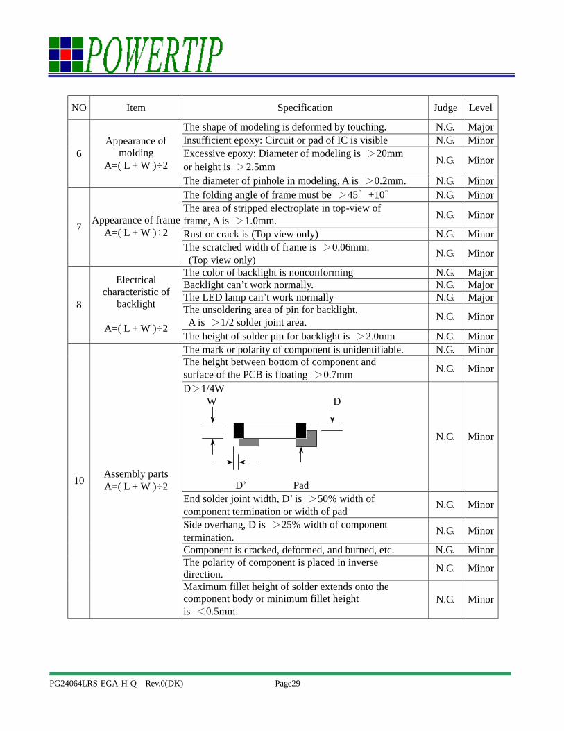
PG24064LRS-EGA-H-Q Rev.0(DK) Page29
NO Item Specification Judge Level
The shape of modeling is deformed by touching. N.G. Major Insufficient epoxy: Circuit or pad of IC is visible N.G. Minor Excessive epoxy: Diameter of modeling is >20mm or height is >2.5mm N.G. Minor 6
Appearance of molding
A=( L + W )÷2 The diameter of pinhole in modeling, A is >0.2mm. N.G. Minor The folding angle of frame must be >45∘+10∘ N.G. Minor The area of stripped electroplate in top-view of frame, A is >1.0mm. N.G. Minor
Rust or crack is (Top view only) N.G. Minor 7 Appearance of frame
A=( L + W )÷2 The scratched width of frame is >0.06mm. (Top view only) N.G. Minor
The color of backlight is nonconforming N.G. Major Backlight can’t work normally. N.G. Major The LED lamp can’t work normally N.G. Major The unsoldering area of pin for backlight, A is >1/2 solder joint area. N.G. Minor
8
Electrical characteristic of
backlight
A=( L + W )÷2 The height of solder pin for backlight is >2.0mm N.G. Minor The mark or polarity of component is unidentifiable. N.G. Minor The height between bottom of component and surface of the PCB is floating >0.7mm N.G. Minor
D>1/4W W D
D’ Pad
N.G. Minor
End solder joint width, D’ is >50% width of component termination or width of pad N.G. Minor
Side overhang, D is >25% width of component termination. N.G. Minor
Component is cracked, deformed, and burned, etc. N.G. Minor The polarity of component is placed in inverse direction. N.G. Minor
10 Assembly parts A=( L + W )÷2
Maximum fillet height of solder extends onto the component body or minimum fillet height is <0.5mm.
N.G. Minor
PG24064LRS-EGA-H-Q Rev.0(DK) Page30
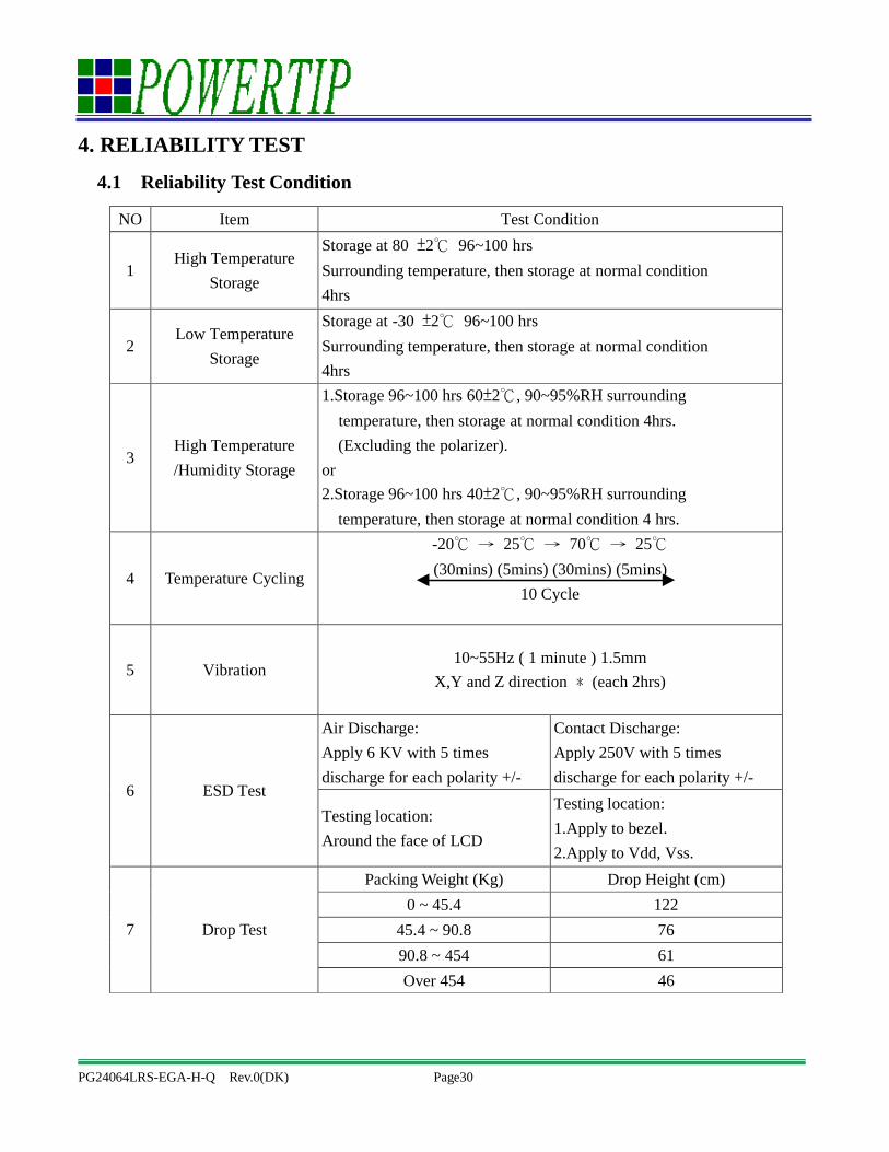
4. RELIABILITY TEST
4.1 Reliability Test Condition
NO Item Test Condition
1 High Temperature
Storage
Storage at 80 ±2 96~100 hrs Surrounding temperature, then storage at normal condition 4hrs
2 Low Temperature
Storage
Storage at -30 ±2 96~100 hrs Surrounding temperature, then storage at normal condition 4hrs
3 High Temperature /Humidity Storage
1.Storage 96~100 hrs 60±2, 90~95%RH surrounding temperature, then storage at normal condition 4hrs.
(Excluding the polarizer). or 2.Storage 96~100 hrs 40±2, 90~95%RH surrounding
temperature, then storage at normal condition 4 hrs.
4 Temperature Cycling
-20 → 25 → 70 → 25 (30mins) (5mins) (30mins) (5mins)
10 Cycle
5 Vibration 10~55Hz ( 1 minute ) 1.5mm
X,Y and Z direction ﹡(each 2hrs)
Air Discharge: Apply 6 KV with 5 times discharge for each polarity +/-
Contact Discharge: Apply 250V with 5 times discharge for each polarity +/-
6 ESD Test Testing location: Around the face of LCD
Testing location: 1.Apply to bezel. 2.Apply to Vdd, Vss.
Packing Weight (Kg) Drop Height (cm) 0 ~ 45.4 122
45.4 ~ 90.8 76 90.8 ~ 454 61
7 Drop Test
Over 454 46
PG24064LRS-EGA-H-Q Rev.0(DK) Page31
5. PRECAUTION RELATING PRODUCT HANDLING 5.1 SAFETY
5.1.1 If the LCD panel breaks , be careful not to get the liquid crystal to touch your skin. 5.1.2 If the liquid crystal touches your skin or clothes , please wash it off immediately by
using soap and water. 5.2 HANDLING
5.2.1 Avoid any strong mechanical shock which can break the glass. 5.2.2 Avoid static electricity which can damage the CMOS LSI—When working with the
module , be sure to ground your body and any electrical equipment you may be using. 5.2.3 Do not remove the panel or frame from the module.
5.2.4 The polarizing plate of the display is very fragile. So , please handle it very carefully ,do not touch , push or rub the exposed polarizing with anything harder than an HB pencil lead (glass , tweezers , etc.)
5.2.5 Do not wipe the polarizing plate with a dry cloth , as it may easily scratch the surface of plate.
5.2.6 Do not touch the display area with bare hands , this will stain the display area. 5.2.7 Do not use ketonics solvent & aromatic solvent. Use with a soft cloth soaked with
a cleaning naphtha solvent. 5.2.8 To control temperature and time of soldering is 280±10and 3-5 sec. 5.2.9 To avoid liquid (include organic solvent) stained on LCM .
5.3 STORAGE 5.3.1 Store the panel or module in a dark place where the temperature is 25 ±5
and the humidity is below 65% RH. 5.3.2 Do not place the module near organics solvents or corrosive gases.
5.3.3 Do not crush , shake , or jolt the module. 5.4 TERMS OF WARRANTY 5.4.1 Applicable warrant period
The period is within thirteen months since the date of shipping out under normal using and storage conditions.
5.4.2 Unaccepted responsibility This product has been manufactured to your company’s specification as a part for use in your company’s general electronic products. It is guaranteed to perform according to delivery specifications. For any other use apart from general electronic equipment , we cannot take responsibility if the product is used in nuclear power control equipment , aerospace equipment , fire and security systems or any other applications in which there is a direct risk to human life and where extremely high levels of reliability are required.