Spark-100 - SOM | Shiratech · 4 | Spark-100 HW user manual v1.2 1 Scope The purpose of this...
40
Spark-100 Altera Cyclone V SOC System on Module Integration guide Revision 1.2
Transcript of Spark-100 - SOM | Shiratech · 4 | Spark-100 HW user manual v1.2 1 Scope The purpose of this...

Spark-100 Altera Cyclone V SOC
System on Module
Integration guide
Revision 1.2

2 | Spark-100 HW user manual v1.2
Contents 1 Scope ..................................................................................................................................................... 4
1.1 SoM introduction ............................................................................................................................. 4
1.2 Block diagram................................................................................................................................... 5
2 Spark-100 Integration guide ................................................................................................................. 6
2.1 Power considerations ...................................................................................................................... 6
2.1.1 VCCBAT - FPGA Encryption Key power .................................................................................... 6
2.1.2 Spark Power scheme ............................................................................................................... 6
2.1.3 Bank 3B and 4A - Programmable Power levels ....................................................................... 7
2.1.4 Bank3A and Bank4A Vref ...................................................................................................... 10
2.2 Reset sources ................................................................................................................................. 10
2.3 HPS Interfaces ................................................................................................................................ 12
2.3.1 USB ........................................................................................................................................ 12
2.3.2 Ethernet port ......................................................................................................................... 13
2.3.3 UART ...................................................................................................................................... 13
2.3.4 CAN ........................................................................................................................................ 13
2.3.5 I2C overview .......................................................................................................................... 14
2.3.6 I2C Mapping .......................................................................................................................... 15
2.3.7 SPI .......................................................................................................................................... 17
2.3.8 JTAG ....................................................................................................................................... 17
2.4 Clocks scheme ................................................................................................................................ 19
2.4.1 Basic clock architecture – SE SOC devices ............................................................................. 19
2.4.2 Advance clock Configuration – SX SOC assembly only .......................................................... 19
2.5 FPGA ............................................................................................................................................... 22
2.5.1 FPGA IOs ................................................................................................................................ 22
2.5.2 Transceivers .......................................................................................................................... 22
2.5.3 FPGA configuration ............................................................................................................... 22
2.6 HPS Memories scheme .................................................................................................................. 23
2.6.1 QSPI NOR memory ................................................................................................................ 24
2.6.2 EEPROM................................................................................................................................. 24
2.6.3 eMMC (iNAND) ...................................................................................................................... 24
2.6.4 SD/eMMC interface............................................................................................................... 25
3 | Spark-100 HW user manual v1.2
2.6.5 Boot options .......................................................................................................................... 25
2.6.6 DDR memory ......................................................................................................................... 25
2.7 Interrupt & I/O Table ..................................................................................................................... 26
2.8 Temperature sensor....................................................................................................................... 26
2.9 Pin assignment ............................................................................................................................... 26
2.10 Mechanical considerations ........................................................................................................ 28
2.10.1 SMARC connector ............................................................................................................. 29
Appendix 1 - Hardware devices used on the SOM ................................................................................. 31
Appendix 2 – Qsys parameters for the Spark ......................................................................................... 32
Document Revision History
Revision Date Description
1.0 12.6.2014 Initial version
1.1 15.8.2014 Fixing and updating various issues
1.11 7.9.2014 Update HPS voltage levels
1.2 16.11.2014 Add Qsys parameters
4 | Spark-100 HW user manual v1.2
1 Scope The purpose of this document is to provide a guide for integrating the Spark-100 into the target
hardware in an easy and fast way to shorten and simplify the development process.
The guide is divided into two parts, the first guide you through the integration process, giving design
samples based on the CB-50 development board (schematics can be provided by Shiratech via
[email protected] ), the second part provides a more detailed description of the Spark-100
system.
In order to simplify the integration process we recommend the following process:
1. Read through the integration guide about the required interfaces.
2. Use Shiratech’s Pin configuration tool to define the solution
3. Use the CB-50 as a reference design and schematics to shorten the development process.
For more details if needed, review the Cyclone V user manual.
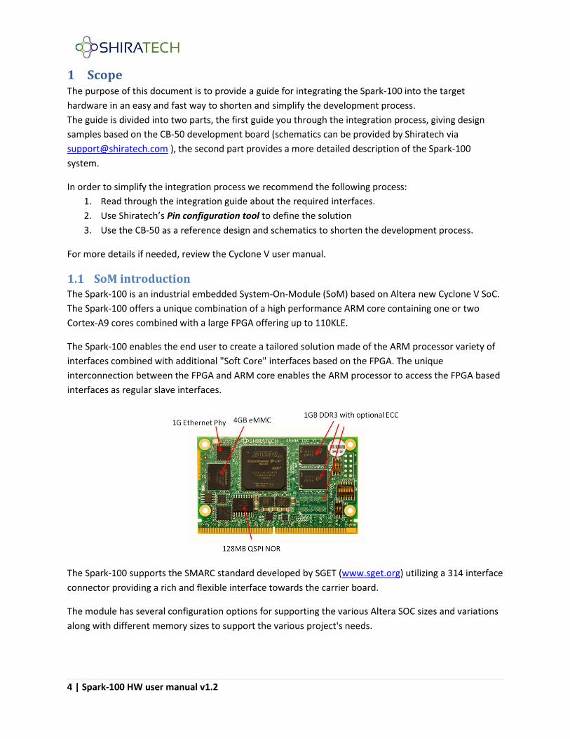
1.1 SoM introduction The Spark-100 is an industrial embedded System-On-Module (SoM) based on Altera new Cyclone V SoC.
The Spark-100 offers a unique combination of a high performance ARM core containing one or two
Cortex-A9 cores combined with a large FPGA offering up to 110KLE.
The Spark-100 enables the end user to create a tailored solution made of the ARM processor variety of
interfaces combined with additional "Soft Core" interfaces based on the FPGA. The unique
interconnection between the FPGA and ARM core enables the ARM processor to access the FPGA based
interfaces as regular slave interfaces.
The Spark-100 supports the SMARC standard developed by SGET (www.sget.org) utilizing a 314 interface
connector providing a rich and flexible interface towards the carrier board.
The module has several configuration options for supporting the various Altera SOC sizes and variations
along with different memory sizes to support the various project's needs.

5 | Spark-100 HW user manual v1.2
1.2 Block diagram The following diagram provides an overview of the SOM. The following paragraphs will provide detailed
description of the various parts of the SOM and how to use them in order to build a product around it.
Figure 1 – SOM main building blocks

6 | Spark-100 HW user manual v1.2
2 Spark-100 Integration guide The HW integration guide covers all the hardware issues related to how to connect the SoM to the
target device starting from power connectivity, connector details, pin-out options, description of the
various interfaces along with a reference design for most of the interfaces. By using the same design as
the reference board you can shorten the BSP development phase and reduce the risk of mistakes. The
reference design is based on the CB-50.
2.1 Power considerations The Spark-100 uses a single 5V power input from which all the other required voltages are taken.?. The
Inlet power should be
Rise time: <= 3ms
Input voltage range: 5V +/- 5%
2.1.1 VCCBAT - FPGA Encryption Key power
The Altera SOC has an option to maintain an encryption key for FPGA configuration even if the system
power is down. For that pin S147 of the SMARC interface should be connected to a power source
(between 1.2V - 3V). If the option is not used connect pin S147 to 2.5V. The interface is connected to
VCCBAT(D7) pin of the SOC.
2.1.2 Spark Power scheme
The SPARK-100 has flexible power architecture to support the ARM core and the FPGA's power
requirements. The following figure describes the power architecture:
1.1V, 4A
Core
1.5V, 4A
DDR3
2.5V
1A
3.3V
0.6A
1.8V
0.6A
Programmable VCCPD
2.5V, 3.3V 0.6A
Vin 5V
HPS Core
FPGA VCC
HPS DDR3
FPGA I/O
FPGA PLL, OSC, I/O
Peripherals
FPGA I/O
Peripherals
Peripherals
FPGA I/O
FPGA VCCPD
Bank 3B, 4A
FPGA I/O
Bank 3B
FPGA I/O
Bank 4A
Programmable VCCIO
1.8V, 2.5V, 3.3V 0.6A
Programmable VCCIO
1.8V, 2.5V, 3.3V 0.6A
PG
7 | Spark-100 HW user manual v1.2
Figure 2 – SOM internal power scheme
The SOM uses both fixed and configurable power converters for powering the HPS and FPGA IO banks.
The following table describes the power levels of available for each I/O bank:
FPGA IO banks:
FPGA bank
Number of I/O
Voltage supported
Remarks
Bank 3A 16 1.8V or 3.3V The default configuration 1.8V.
For other options contact [email protected]
Bank 3B 32 1.5V, 1.8V, 2.5V, 3.3V The selection is done by hardware and cannot be changed during operation.
Bank 4A 68 1.5V, 1.8V, 2.5V, 3.3V The selection is done by hardware and cannot be changed during operation.
Bank 5A 16 1.8V Fix
Bank 5B 7 3.3V Fix
Bank 8A 6 1.8V Fix
HPS IO banks:
HPS bank Voltage supported Remarks
Bank 6 1.5v Internal bank for DDR
7A 1.8V Various interfaces,
7B, 7C 3.3V Various interfaces, like SD and USB
2.1.3 Bank 3B and 4A - Programmable Power levels
The power of banks 3B and 4A can be programmed according to the design requirements. Each bank in
the FPGA has a VCCPD and a VCCIO that control the banks power level. Banks 3B and 4A share a single

8 | Spark-100 HW user manual v1.2
VCCPD (FPGA architecture) while each bank has its own VCCIO. This adds some limitation to the banks
power levels options. The following table describes the various possibilities:
VCCPD Bank 3B Bank 4A
Set to 3.3V 3.3V only 3.3V only
Set to 2.5V 1.5V, 2.5V or 1.8V 1.5V, 2.5V or 1.8V
The power option required can be set in two ways either via switches located on the SOM (can be used
for debug and prototype) or via pins on the SMARC interface – this option must be used in production.
Note - the pins cannot be based on I/Os set by software the pin state should be stable at power up
and cannot be changed after power up!
Figure 3 - Bank 3B/4A Power Switching scheme
DC to DC
3.3, 2.5, 1.8V
1.5V FPGA
Power
Switch
Power
Switch
Programmable VCCIO
Bank 3B
1.5V, 1.8V, 2.5V, 3.3V 0.6A
1 2
3
ON
ON
VCCIO
Bank 3B
DC to DC
3.3, 2.5, 1.8V
1.5V FPGA
Power
Switch
Power
Switch
Programmable VCCIO
Bank 4A
1.5V, 1.8V, 2.5V, 3.3V 0.6A
1 4
5
ON
ON
VCCIO
Bank 4A

9 | Spark-100 HW user manual v1.2
2.1.3.1 Setting the power levels via the SMARC connector
The following table describes the setting of each pin for any available operation voltage. Note that all
ports have internal pull up on the SOM.
Port Pin (SMARC)
3.3V
2.5V 1.8V 1.5V
3B - Select 0 P73 Ground Ground Open Open
3B - Select 1 P74 Open Open Open Ground
4A - Select 0 P76 Ground Ground Open Open
4A - Select 1 P81 Open Open Open Ground
VCCPD_SEL_C S77 Open Ground Ground Ground
2.1.3.2 Setting the power levels via the internal switches
The power levels of ports 3B and 4A can be set by dip switches located on the SPARK-100 board (SW2).
There is a single switch that sets the VCCPD power for both banks and two switches that set the power
of the VCCIO for each bank.
The following figures describe how to set the switch to the various options:
The following figures describe power schemes where the VCCPD is set to 3.3V.
Figure 4 - Bank 3B and 4A VCCPD is 3.3V
The following figures describe power schemes where the VCCPD is set to 2.5V.
Programmable VCCPD
Bank 3B, 4A
2.5V, 3.3V 0.6A
ON
1 2 3 4 5
3.3 V Programmable VCCIO
Bank 3B
1.5V, 1.8V, 2.5V, 3.3V 0.6A
Programmable VCCIO
Bank 4A
1.5V, 1.8V, 2.5V, 3.3V 0.6A
ON
1 2 3 4 5
ON
1 2 3 4 5
Only 3.3 V
Only 3.3 V
MUST
MUST

10 | Spark-100 HW user manual v1.2
Figure 5 - Bank 3B and 4A VCCPD is 2.5V
When the VCCPD is set to 2.5V, each I/O can be separately set to 1.5V, 1.8V or 2.5V. Figure 5 describes
two configurations in which the VCCPD is set to 2.5V.
In the top configuration Bank 3B's VCCIO is set to 2.5V and Bank 4A's VCCIO is set to 1.8V. In the bottom
configuration Bank 3B's VCCIO is set to 1.8V and Bank 4A's VCCIO is set to 1.5V.
2.1.4 Bank3A and Bank4A Vref
Bank3B and Bank4A can support an external DDR3 interface assembled on the carrier board. The DDR
requires reference voltage from the FPGA. These signals are available through the SMARC connector
VREF_3B (P104) and VREF_4B (P105). If this option is not used these pins should be tied to ground.
2.2 Reset sources The SPARK-100 supports three reset sources:
Cold reset (RESET_IN# – P127 on the SMARC interface) o Used to ensure the HPS is placed in a default state sufficient for software to boot o Triggered by a power-on reset and other sources e.g. push buttons on carrier board o Resets all HPS logic that can be reset o Affects all reset domains o This Reset is provided to the carrier board via P126
Warm reset (FORCE_RECOV# - S155 on the SMARC interface) o Occurs after HPS has already been through a cold reset o Used to recover system from a non-responsive condition o Resets a subset of the HPS state reset by a cold reset o Only affects the system reset domain, which allows debugging (including trace) to
operate through the warm reset
Debug Reset o Occurs after HPS has already been through a cold reset o Used to recover debug logic from a non-responsive condition o Only affects the debug reset domain
Programmable VCCPD
Bank 3B, 4A
2.5V, 3.3V 0.6A
ON
1 2 3 4 5
2.5 V Programmable VCCIO
Bank 3B
1.5V, 1.8V, 2.5V, 3.3V 0.6A
Programmable VCCIO
Bank 4A
1.5V, 1.8V, 2.5V, 3.3V 0.6A
ON
1 2 3 4 5
ON
1 2 3 4 5
2.5 V
1.8 V
ON
1 2 3 4 5
1.5 V
1.8 VProgrammable VCCIO
Bank 3B
1.5V, 1.8V, 2.5V, 3.3V 0.6A
Programmable VCCIO
Bank 3B
1.5V, 1.8V, 2.5V, 3.3V 0.6A

11 | Spark-100 HW user manual v1.2
The cold and warm resets are controlled by voltage supervisors which guarantee the reset duration.
Both signals are available on the SMARC connector.
The FPGA can also be reset by the SOC ARM core or by an IO pin on the FPGA fabric.
When using the 128 MB QSPI Flash memory as a boot source the warm reset does not work
automatically due to configuration issues of the QSPI memory. For more details:
http://www.rocketboards.org/foswiki/Documentation/SocBoardQspiBoot
For 32MB QSPI Flash memory configuration the problem is resolved.

12 | Spark-100 HW user manual v1.2
2.3 HPS Interfaces The Spark-100 offers a variety of interfaces from the HPS (SOC ARM core) such as USB, Ethernet, I2C,
SPI, UART and more. The following paragraphs describe the various interfaces available along with
recommendations on how to connect them to the carrier board.
2.3.1 USB
The SPARK-100 uses a single Host/Device (USB1) of the HPS. The USB port on the HPS features the
following:
Supports USB 2.0 host and device operation
Dual-role device (device and host functions)
High-speed (480 Mbps)
Full-speed (12 Mbps)
Low-speed (1.5 Mbps)
Supports USB 1.1 (full-speed & low-speed)
Integrated descriptor-based scatter-gather DMA (SGDMA)
Up to 16 bidirectional endpoints, including control endpoint
Up to 16 host channels
Supports generic root hub
Automatic ping capability
Configurable to OTG 1.3 and OTG 2.0
The card has two possible configurations for the USB usage based on internal USB switch (see figure 6):
A single OTG port.
Two host ports using an internal HUB.
The selection is done using IO pin 0-0 of the I2C I/O expender.
HPS
USB PHY
OTG
(USB3300)
Data[0..7]
Ctrl
USB Switch
(USB3740)
USB
USB HUB
(USB2422)
OTG
Host
Host
USB_HUB_OTG_SEL (U19)
Module Carrier
Figure 6 - HPS USB Interfaces
A USB PHY device (USB3300 Microchip) is used to convert the HPS ULPI interface into a USB OTG
interface. The USB OTG output is then connected to an analog USB switch (USB 3740). The switch
connects the USB OTG interface directly to the SAMRC interface or to an internal USB HUB.
The internal USB HUB (USB2422) is a two ports HUB providing two USB Host interfaces over the SMARC
connector.

13 | Spark-100 HW user manual v1.2
The default configuration of the USB switch enables the USB HUB interface.
Each of the USB interfaces provides control signals (Power_EN, Over_Current) for controlling an external
USB power distributer located on the carrier board.
2.3.2 Ethernet port
The SPARK-100 supports a single 10/100/1000 Ethernet interface from the HPS (RGMII 1). The Ethernet
Phy in connected via an RGMII interface to the HPS. The following figure describes the Giga Ethernet
interface.
Figure 8 - Giga Ethernet & Fast Ethernet Interfaces
The Ethernet PHY is KSZ9031 by Micrel. It uses an RGMII interface running at 125MHz. The 125 MHz
clock is generated by the Ethernet PHY.
The Ethernet PHY analog signals (TX+/-, RX+/-) are connected the SMARC edge connector. Two LED
signals from the GE PHY are also connected to the SMARC edge connector. MDC/MDIO - The Ethernet
MDC/MDIO signals are connected to the internal phy and are not available on the SMARC connector.
2.3.3 UART
The SOM offer one or two UARTs. Each UART includes Rx, Tx , CTS and RTS. The HPS supports up to two
UART interfaces. UART 0 is usually used for Linux CLI interface. Some of the UART signals share the same
pins as the SPI interfaces which available on the SMARC connector.
Programmable character properties, such as number of data bits per character, optional parity bits, and number of stop bits.
Programmable baud rate.
Automatic flow control mode per 16750 standard.
The maximum UART baud rate is 6.25 mega symbols per second.
2.3.4 CAN
The HPS offers up to two CAN controllers based on the Bosch® D_CAN controller and offer the following
features:
HPS
Micrelksz9031
RGMII4 x TX
4 x RX
Controls
125 Mhz
25M
Int.
NReset
LEDS LEDS
GE Analog
CarrierModule

14 | Spark-100 HW user manual v1.2
Compliant with CAN protocol specification 2.0 part A & B.
Programmable communication rate up to 1 Mbps.
Holds up to 128 messages.
Supports 11-bit standard and 29-bit extended identifiers.
Programmable interrupt scheme.
Direct access for host processor.
DMA controller may be used for large transfers.
2.3.5 I2C overview
The Spark-100 uses two I2C buses of the HPS. The HPS offers the following I2C support:
- Maximum clock speed of up to 400 Kbps. - 7- or 10-bit addressing. - Mixed read and write combined-format transactions in both 7-bit and 10-bit addressing mode. - Bulk transmit mode. - Transmit and receive buffers. - Handles bit and byte waiting at all bus speeds. - DMA handshaking interface.
On the SPARK the I2C buses are used as follows:
I2C0 is expanded to four I2C interfaces in order to meet the SMARC requirements providing I2C_Cam, I2C_GP, I2C_PM and I2C_LCD buses.
o The buses can be used for any other application according need. o There are pull-up resistors on each bus, so there no need to put pull-up resistors on the
carrier board. o The expansion is done using TI TCA9548A (8 channel I2C switch). Buses 0-3 of the device
are connected to the SAMRC connector, the other buses are unused.
I2C1 is connected to the I2C controlled chips on the SOM and is not available externally. There are several devices located on I2C1 bus:
o An I2C I/O expender using TI TCA9548A, for providing additional GPIOs for control and monitor
o An E2PROM device Atmel AT24C01C, used for system parameters storage. o Control interface for the advanced clock distributor, the CDCM6208 by TI (assembled
only for SOM with Altera SX device) . o A Digital Temperature Sensor for monitoring system temperature. The device used is TI
TMP108.

15 | Spark-100 HW user manual v1.2
Figure 9 - SPARK-100 I2CInterfaces
2.3.6 I2C Mapping
2.3.6.1 I2C0 Expander Ports Allocation
The HPS I2C0 interface is connected to an I2C bus expander. The following table describes the I2C
expender ports allocation.
Port Signals Description
0 I2C_CAM_D I2C_CAM _C
Enables access to I2C devices on Carrier I2C_CAM in SMARC standard
1 I2C_GP_D I2C_GP _C
Enables access to I2C devices on Carrier I2C_GP in SMARC standard
2 I2C_PM_D I2C_PM _C
Enables access to I2C devices on Carrier I2C_PM in SMARC standard
3 I2C_LCD_D I2C_LCD _C
Enables access to I2C devices on Carrier I2C_LCD in SMARC standard
4-7 Not Connected
HPS
Temp
Sens
Clk
Gen.
I/O
Exp.
EEP
ROM
I2C
ExpanderI2C0
I2C1
CarrierModule
I2C_CAM
I2C_GP
I2C_PM
I2C_LCD
IO
EXP

16 | Spark-100 HW user manual v1.2
The I2C expander address is
0xE1 Read 0xE0 Write
2.3.6.2 I2C1 I/O Expander
The HPS I2C1 interface is connected to an I/O expander to enable more GPIO for control. The following
table provides mapping of the I/Os:
Port Signal Type Description
0-0 USB_HUB_OTG_SEL Out Select between USB OTG and USB HUB "0" – OTG "1" – HUB
0-1 Main_CLK_SEL
Out Do not use leave as input!
0-2 REF_CLK_SEL Out Select the clock generator source clock . "0" – Primary (internal) "1" – Secondary (external)
0-3 CLK_SYNC Out Synchronize the clock generator
0-4 CLK_PDN Out Disable the clock generator(clock generator ) "0" – Disable "1" – Enabled
0-5 CLK_RESETN Out Reset the clock generator(clock generator) "0" – Reset "1" – Normal
0-6 0-7
Not in Use
1-0 – 1-5 Connected to SMARC connector as GPIOs
Out User define
1-6 SATA_ACT# Out SATA is active (When available) "0" – Off "1" – on
1-7
INT1_A
Out On board debug Led "0" – off "1" – On
2.3.6.3 I2C Address table
The following table describes the I2C addresses mapping:
1 1 1 0 0 0 0 RW

17 | Spark-100 HW user manual v1.2
2.3.7 SPI
The SPARK-100 supports up to two SPI interfaces. Each port offers:
Single CS signal for each SPI interface.
Programmable master serial bit rate up to 50 MHZ.
Serial master
Programmable data item size of 4 to 16 bits Note – When the SPI interfaces are not in use, the pins can be configured as a GPIOs.
2.3.8 JTAG
The SPARK-100 integrates an optional on board 10 pins JTAG connector. The JTAG signals are also
connected to the SMARC connector, an analog switch selects between the JTAG connector and the
SMARC connector. The selection is done by a switch located on the SOM (SW3).
The following figure describes the JTAG chain:
Ref. Chip I2C Port Address A Port Address B Description
Ux PCA9548 0 1 1 1 0 0 0 0 RW I2C Interface Expander
SMARC 0 1 1 1 0 0 0 0 RW 0 X X X X X X X RW
I2C_CAM
0 1 1 1 0 0 0 0 RW 1 X X X X X X X RW
I2C_GP
0 1 1 1 0 0 0 0 RW 2 X X X X X X X RW
I2C_PM
0 1 1 1 0 0 0 0 RW 3 X X X X X X X RW
I2C_LCD
Ux TCA6416A 1 0 1 0 0 0 0 0 RW 20 H
I2C I/O Expander
Ux Temp Sens 1 1 0 0 1 0 0 0 RW 48 H Temperature Sensor
Ux CLK_Gen 1 1 0 1 0 1 0 0 RW 54 H Clock Generator
Ux EEPROM 1 1 0 1 0 0 0 0 RW 50 H EEPROM

18 | Spark-100 HW user manual v1.2
Figure 12 - SPARK-100 JTAG chain
A second switch can set the JTAG chain to include the HPS and FPGA or just the HPS. Both switches are
located in SW3 (see picture below)
The switches options are as follows:
JSEL0 0 FPGA in Chain (default) 1 FPGA not in chain JSEL1 0 JTAG connector (default) 1 SMARC connector
Note: For production, the SOM provided without the JTAG connector; in that case the JTAG interface will
be available only on the SMARC interface.
Analog
Switch
TS3A5015
HPS
FPGA
Analog
Switch
TS3A5015
ModuleCarrier
JTAG_I/O
JTAG
I/O
TDI
TDI
TDO
TDO
TDO
SW - 2
SW - 1
The left pin
is JSEL 1, the
Lower side is
off - '0'
19 | Spark-100 HW user manual v1.2
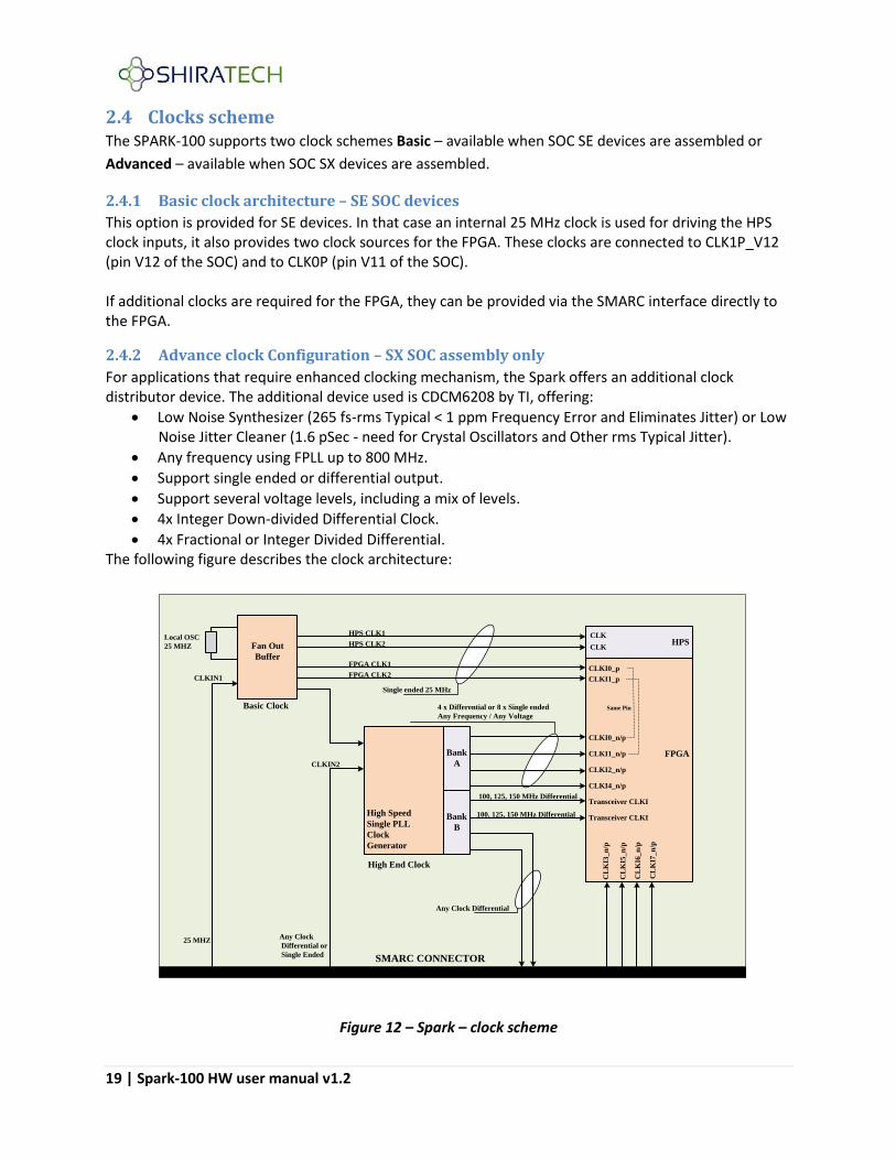
2.4 Clocks scheme The SPARK-100 supports two clock schemes Basic – available when SOC SE devices are assembled or
Advanced – available when SOC SX devices are assembled.
2.4.1 Basic clock architecture – SE SOC devices
This option is provided for SE devices. In that case an internal 25 MHz clock is used for driving the HPS clock inputs, it also provides two clock sources for the FPGA. These clocks are connected to CLK1P_V12 (pin V12 of the SOC) and to CLK0P (pin V11 of the SOC). If additional clocks are required for the FPGA, they can be provided via the SMARC interface directly to the FPGA.
2.4.2 Advance clock Configuration – SX SOC assembly only
For applications that require enhanced clocking mechanism, the Spark offers an additional clock distributor device. The additional device used is CDCM6208 by TI, offering:
Low Noise Synthesizer (265 fs-rms Typical < 1 ppm Frequency Error and Eliminates Jitter) or Low Noise Jitter Cleaner (1.6 pSec - need for Crystal Oscillators and Other rms Typical Jitter).
Any frequency using FPLL up to 800 MHz.
Support single ended or differential output.
Support several voltage levels, including a mix of levels.
4x Integer Down-divided Differential Clock.
4x Fractional or Integer Divided Differential. The following figure describes the clock architecture:
Figure 12 – Spark – clock scheme
Fan Out
Buffer
HPS CLK1
HPS CLK2
FPGA CLK1
FPGA
CLKIN1
High Speed
Single PLL
Clock
Generator
CLKIN2
Bank
A
Bank
B
SMARC CONNECTOR
HPS
FPGA CLK2CLKI0_p
CLKI1_p
CLKI0_n/p
CLKI1_n/p
CLKI2_n/p
CLKI4_n/p
Transceiver CLKI
Transceiver CLKI
Single ended 25 MHz
4 x Differential or 8 x Single ended
Any Frequency / Any Voltage
100, 125, 150 MHz Differential
100, 125, 150 MHz Differential
Any Clock Differential
25 MHZ
Local OSC
25 MHZ
CL
KI3
_n
/p
CLK
CLK
CL
KI5
_n
/p
CL
KI6
_n
/p
CL
KI7
_n
/p
Basic Clock
High End Clock
Any Clock
Differential or
Single Ended
Same Pin
20 | Spark-100 HW user manual v1.2
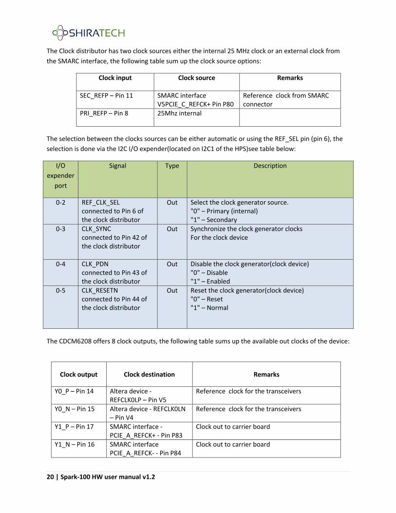
The Clock distributor has two clock sources either the internal 25 MHz clock or an external clock from
the SMARC interface, the following table sum up the clock source options:
Clock input
Clock source Remarks
SEC_REFP – Pin 11 SMARC interface V5PCIE_C_REFCK+ Pin P80
Reference clock from SMARC connector
PRI_REFP – Pin 8 25Mhz internal
The selection between the clocks sources can be either automatic or using the REF_SEL pin (pin 6), the
selection is done via the I2C I/O expender(located on I2C1 of the HPS)see table below:
I/O
expender
port
Signal Type Description
0-2 REF_CLK_SEL connected to Pin 6 of the clock distributor
Out Select the clock generator source. "0" – Primary (internal) "1" – Secondary
0-3 CLK_SYNC connected to Pin 42 of the clock distributor
Out Synchronize the clock generator clocks For the clock device
0-4 CLK_PDN connected to Pin 43 of the clock distributor
Out Disable the clock generator(clock device) "0" – Disable "1" – Enabled
0-5 CLK_RESETN connected to Pin 44 of the clock distributor
Out Reset the clock generator(clock device) "0" – Reset "1" – Normal
The CDCM6208 offers 8 clock outputs, the following table sums up the available out clocks of the device:
Clock output Clock destination Remarks
Y0_P – Pin 14 Altera device - REFCLK0LP – Pin V5
Reference clock for the transceivers
Y0_N – Pin 15 Altera device - REFCLK0LN – Pin V4
Reference clock for the transceivers
Y1_P – Pin 17 SMARC interface -PCIE_A_REFCK+ - Pin P83
Clock out to carrier board
Y1_N – Pin 16 SMARC interface PCIE_A_REFCK- - Pin P84
Clock out to carrier board
21 | Spark-100 HW user manual v1.2
Y2_P – Pin 20 Altera device – REFCLK1LP – Pin P8
Reference clock for the transceivers
Y2_N – Pin 21 Altera device – REFCLK1LN – Pin N8
Ref clock for the transceivers
Y3_P – Pin 20 SMARC interface -PCIE_B_REFCK+ - Pin S84
Clock out to carrier board
Y3_N – Pin 21 SMARC interface -PCIE_B_REFCK- - Pin S85
Clock out to carrier board
Y4_P – Pin 26 Altera device – CLK0P – Pin V11
FPGA clock input. If a single ended clock is needed, use the P pin only!
Y4_N – Pin 25 Altera device – CLK0N – Pin W11
FPGA clock input.
Y5_P – Pin 29 Altera device – CLK1P – Pin V12
FPGA clock input. If a single ended clock is needed, use the P pin only!
Y5_N – Pin 28 Altera device – CLK1N – Pin W12
FPGA clock input.
Y6_P – Pin 32 Altera device – CLK2P – Pin Y13
FPGA clock input. If a single ended clock is needed, use the P pin only!
Y6_N – Pin 33 Altera device – CLK2N – Pin AA13
FPGA clock input.
Y7_P – Pin 35 Altera device – CLK4P – Pin Y24
FPGA clock input. If a single ended clock is needed, use the P pin only!
Y7_N – Pin 36 Altera device – CLK4N – Pin W24
FPGA clock input.
Note: If a single ended clock is required only the P line of the clock should be used.

22 | Spark-100 HW user manual v1.2
2.5 FPGA The Spark 100 offer a range of FPGA sizes starting from 25KLEs and up to 110KLEs. The FPGA offers 145
I/Os and optionally additional 6 high speed transceivers.
2.5.1 FPGA IOs
The I/Os available are divided to banks according to the following table:
FPGA bank Number of I/O Voltage supported
Bank 3A 16 1.8V
Bank 3B 32 1.5V, 1.8V, 2.5V, 3.3V
Bank 4A 68 1.5V, 1.8V, 2.5V, 3.3V
Bank 5A 16 1.8V
Bank 5B 7 3.3V
Bank 8A 6 1.8V
Note: All FPGA GPIO which can be differential pairs are routed as pairs to the SMARC connector.
2.5.2 Transceivers
The CycloneV SX family provides 6 transceivers at 3.125 Gigabits per second (Gbps). These transceivers
comply with a wide range of protocols and data rate standards.
On the Spark the transceivers are routed as differential pairs to support high speed applications. The
Spark also provide optional low jitter differential clock using a build in clock generator, with an option to
provide differential clocks.
2.5.3 FPGA configuration
The FPGA can be configured in several ways:
2.5.3.1 Configuration via byte blaster
The Spark has an option for a build in JTAG connector for connecting the byte blaster (for development
boards only), alternatively a byte blaster can be connected via the SMARC interface. For more details
see the paragraph 2.3.8 on JTAG interface.
2.5.3.2 Configuration via Software
The FPGA can be easily configured via Software. The FPGA file should be placed in the FAT part of the SD
used for software. The FPGA file should be in FPP 16(Fast parallel 16 bits), security disable, compression
disable, RBF format, the file should be called fpga.rbf. The FPGA will be programed by the boot software,
23 | Spark-100 HW user manual v1.2
which means that FPGA download can be done without any customization of the SW thus ot provides
total decoupling between the SW and HW development.
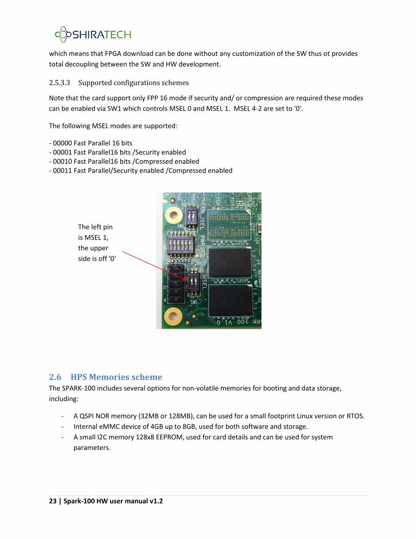
2.5.3.3 Supported configurations schemes
Note that the card support only FPP 16 mode if security and/ or compression are required these modes
can be enabled via SW1 which controls MSEL 0 and MSEL 1. MSEL 4-2 are set to '0'.
The following MSEL modes are supported:
- 00000 Fast Parallel 16 bits - 00001 Fast Parallel16 bits /Security enabled - 00010 Fast Parallel16 bits /Compressed enabled - 00011 Fast Parallel/Security enabled /Compressed enabled
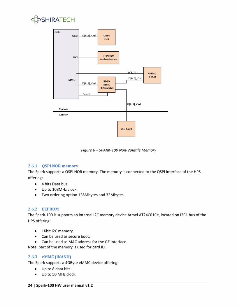
2.6 HPS Memories scheme The SPARK-100 includes several options for non-volatile memories for booting and data storage,
including:
- A QSPI NOR memory (32MB or 128MB), can be used for a small footprint Linux version or RTOS.
- Internal eMMC device of 4GB up to 8GB, used for both software and storage.
- A small I2C memory 128x8 EEPROM, used for card details and can be used for system
parameters.
The left pin
is MSEL 1,
the upper
side is off '0'
24 | Spark-100 HW user manual v1.2
Figure 6 – SPARK-100 Non-Volatile Memory
2.6.1 QSPI NOR memory
The Spark supports a QSPI NOR memory. The memory is connected to the QSPI interface of the HPS
offering:
4 bits Data bus.
Up to 108MHz clock.
Two ordering option 128Mbytes and 32Mbytes.
2.6.2 EEPROM
The Spark-100 is supports an internal I2C memory device Atmel AT24C01Ce, located on I2C1 bus of the
HPS offering:
1Kbit I2C memory.
Can be used as secure boot.
Can be used as MAC address for the GE interface. Note: part of the memory is used for card ID.
2.6.3 eMMC (iNAND)
The Spark supports a 4GByte eMMC device offering:
Up to 8 data bits.
Up to 50 MHz clock.
HPS
eMMC
4-8GB
QSPI
1Gb
SDIO
MUX
(TXS02612)
EEPROM
Authentication
QSPI D[0..3]. Ctrl
I2C1
MMC
D[0..3], Ctrl
D[0..3], Ctrl
D[0..3], Ctrl
D[4..7]
uSD Card
Module
Carrier
Select
25 | Spark-100 HW user manual v1.2
An 8GByte option is available as an ordering option.
2.6.4 SD/eMMC interface
The SPARK-100 has a single SD/MMC bus connected to the HPS. The HPS is connected via an internal
multiplexer (TXS02612 - SDIO Port Expander by TI) to either an internal 4/8 bits wide eMMC or to an
external 4 bits SD interface.
The control of the mux is done by GPIO44 of the HPS, ‘0’ – eMMC, ‘1’ - external SD. The mux can be
controlled also via an external pin P123 in the SMARC interface.
The pin can be tight to the required mode or alternatively in order to leave the control to the software
connect to an external pull up or pull down according to the required mode.
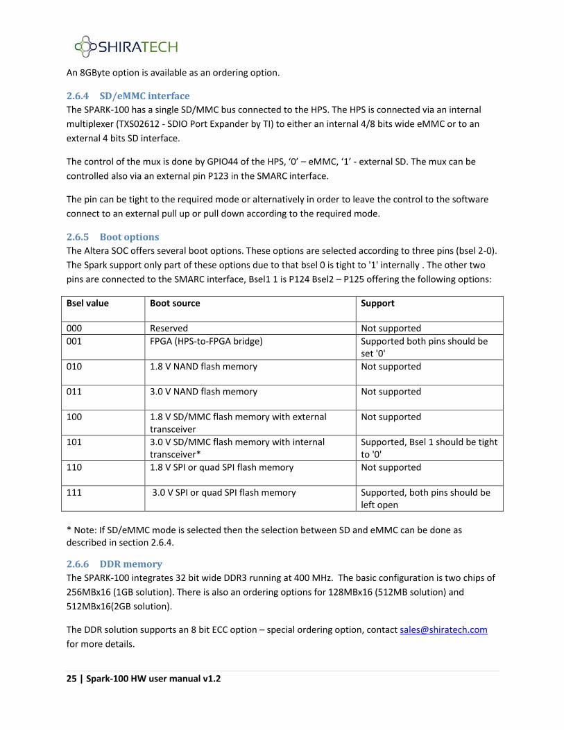
2.6.5 Boot options
The Altera SOC offers several boot options. These options are selected according to three pins (bsel 2-0).
The Spark support only part of these options due to that bsel 0 is tight to '1' internally . The other two
pins are connected to the SMARC interface, Bsel1 1 is P124 Bsel2 – P125 offering the following options:
Bsel value
Boot source Support
000 Reserved Not supported
001 FPGA (HPS-to-FPGA bridge) Supported both pins should be set '0'
010
1.8 V NAND flash memory Not supported
011
3.0 V NAND flash memory Not supported
100 1.8 V SD/MMC flash memory with external transceiver
Not supported
101 3.0 V SD/MMC flash memory with internal transceiver*
Supported, Bsel 1 should be tight to '0'
110 1.8 V SPI or quad SPI flash memory
Not supported
111 3.0 V SPI or quad SPI flash memory Supported, both pins should be left open
* Note: If SD/eMMC mode is selected then the selection between SD and eMMC can be done as described in section 2.6.4.
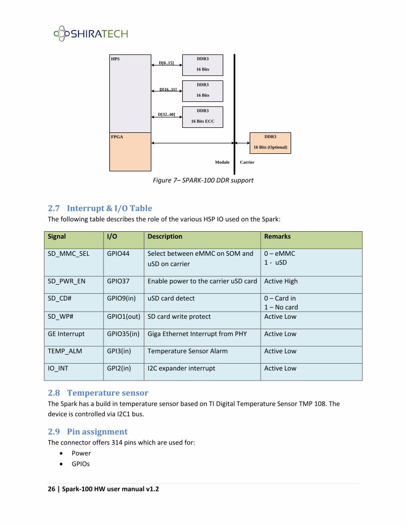
2.6.6 DDR memory
The SPARK-100 integrates 32 bit wide DDR3 running at 400 MHz. The basic configuration is two chips of
256MBx16 (1GB solution). There is also an ordering options for 128MBx16 (512MB solution) and
512MBx16(2GB solution).
The DDR solution supports an 8 bit ECC option – special ordering option, contact [email protected]
for more details.
26 | Spark-100 HW user manual v1.2
Figure 7– SPARK-100 DDR support
2.7 Interrupt & I/O Table The following table describes the role of the various HSP IO used on the Spark:
Signal I/O Description Remarks
SD_MMC_SEL GPIO44 Select between eMMC on SOM and
uSD on carrier
0 – eMMC 1 - uSD
SD_PWR_EN GPIO37 Enable power to the carrier uSD card Active High
SD_CD# GPIO9(in) uSD card detect 0 – Card in 1 – No card
SD_WP# GPIO1(out) SD card write protect Active Low
GE Interrupt GPIO35(in) Giga Ethernet Interrupt from PHY Active Low
TEMP_ALM GPI3(in) Temperature Sensor Alarm Active Low
IO_INT GPI2(in) I2C expander interrupt Active Low
2.8 Temperature sensor The Spark has a build in temperature sensor based on TI Digital Temperature Sensor TMP 108. The
device is controlled via I2C1 bus.
2.9 Pin assignment The connector offers 314 pins which are used for:
Power
GPIOs
HPS
FPGA
DDR3
16 Bits
DDR3
16 Bits
DDR3
16 Bits ECC
DDR3
16 Bits (Optional)
Module Carrier
D[0..15]
D[16..31]
D[32..40]

27 | Spark-100 HW user manual v1.2
Fixed interfaces like GE and USB
RFU - unused pins reserved for future use.
The full pin out of the Spark is available in a dedicated document “SPARK pin out definition” available on
the Shiratech web site.
28 | Spark-100 HW user manual v1.2
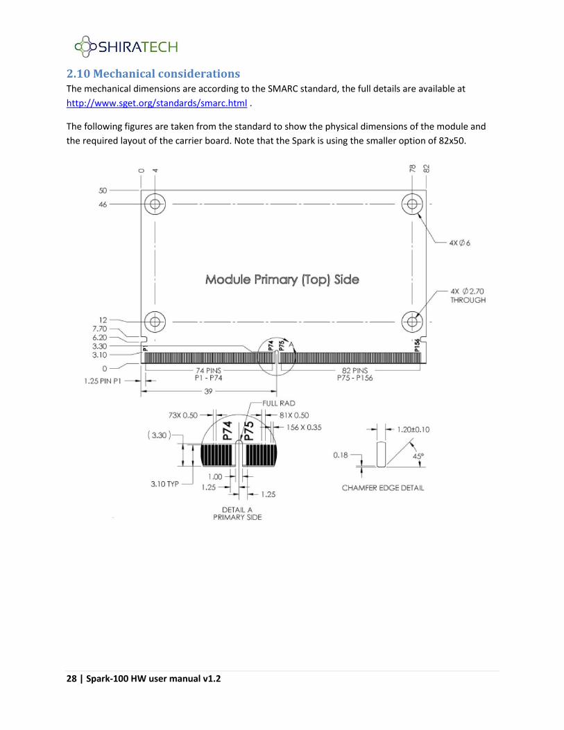
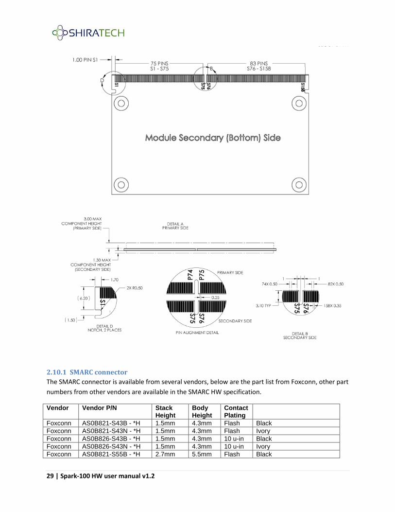
2.10 Mechanical considerations The mechanical dimensions are according to the SMARC standard, the full details are available at
http://www.sget.org/standards/smarc.html .
The following figures are taken from the standard to show the physical dimensions of the module and
the required layout of the carrier board. Note that the Spark is using the smaller option of 82x50.
29 | Spark-100 HW user manual v1.2
2.10.1 SMARC connector
The SMARC connector is available from several vendors, below are the part list from Foxconn, other part
numbers from other vendors are available in the SMARC HW specification.
Vendor Vendor P/N Stack Height
Body Height
Contact Plating
Foxconn AS0B821-S43B - *H 1.5mm 4.3mm Flash Black
Foxconn AS0B821-S43N - *H 1.5mm 4.3mm Flash Ivory
Foxconn AS0B826-S43B - *H 1.5mm 4.3mm 10 u-in Black
Foxconn AS0B826-S43N - *H 1.5mm 4.3mm 10 u-in Ivory
Foxconn AS0B821-S55B - *H 2.7mm 5.5mm Flash Black

30 | Spark-100 HW user manual v1.2
Foxconn AS0B821-S55N - *H 2.7mm 5.5mm Flash Ivory
Foxconn AS0B826-S55B - *H 2.7mm 5.5mm 10 u-in Black
Foxconn AS0B826-S55N - *H 2.7mm 5.5mm 10 u-in Ivory
Foxconn AS0B821-S78B - *H 5.0mm 7.8mm Flash Black
Foxconn AS0B821-S78N - *H 5.0mm 7.8mm Flash Ivory
Foxconn AS0B826-S78B - *H 5.0mm 7.8mm 10 u-in Black
Foxconn AS0B826-S78N - *H 5.0mm 7.8mm 10 u-in Ivory

31 | Spark-100 HW user manual v1.2
Appendix 1 - Hardware devices used on the SOM
Chip Vendor Details CDCM6208 TI 2:8 clock generator , jitter cleaner with fractional dividers
TCA9548A TI Low Voltage 8-Channel I2C Switch With Reset
MT29F1G01AAADD Micron NOR Flash Memory - Serial Peripheral Interface (SPI)
TXS02612 TI SDIO port expander with voltage level translation
AT24C01C Atmel I2C-Compatible (2-wire) Serial EEPROM 1-Kbit (128 x 8)
USB3300 Microchip High speed USB host device or OTG phy
USB3740 Microchip High Speed USB 2.0 Switch with ESD Protection and Low Standby Current
TMP108 TI Low Power Digital Temperature Sensor With Two-Wire Serial Interface in WCSP
TCA9548A TI Low voltage 8-channel I2C switch
USB2422 Microchip 2-Port USB 2.0 Hi-Speed Hub Controller
KSZ9031RN
Micrel 1G Ethernet Physical layer chip

32 | Spark-100 HW user manual v1.2
Appendix 2 – Qsys parameters for the Spark The following paragraph provides the HPS configuration used in the demo version provided for the
Spark.
33 | Spark-100 HW user manual v1.2
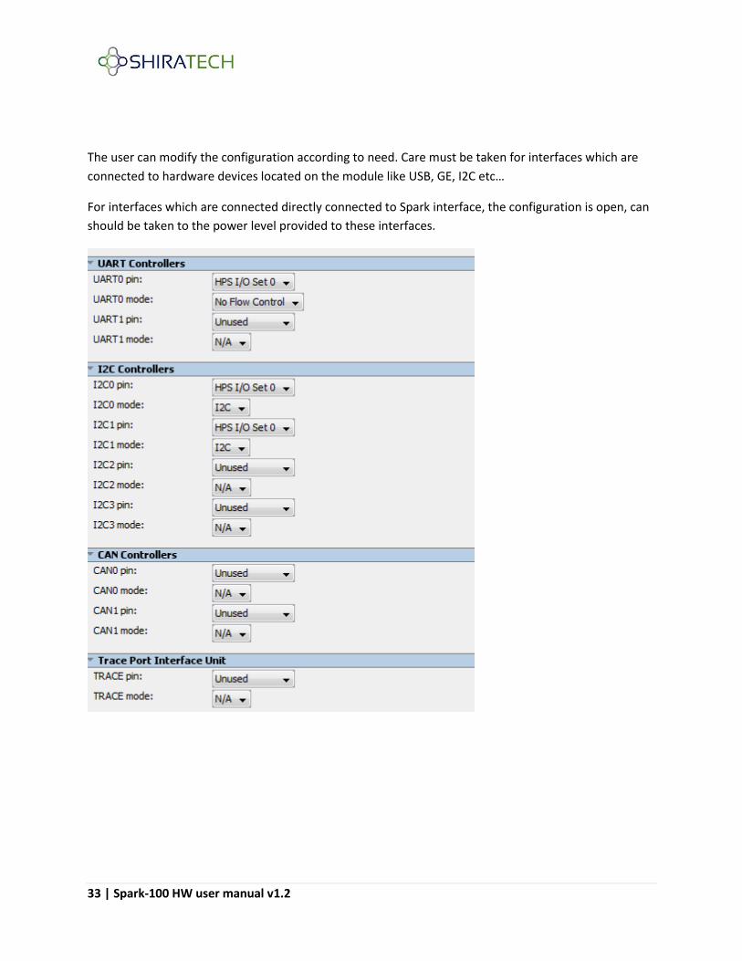
The user can modify the configuration according to need. Care must be taken for interfaces which are
connected to hardware devices located on the module like USB, GE, I2C etc…
For interfaces which are connected directly connected to Spark interface, the configuration is open, can
should be taken to the power level provided to these interfaces.

34 | Spark-100 HW user manual v1.2
Clock configuration:

35 | Spark-100 HW user manual v1.2
DDR setting:

36 | Spark-100 HW user manual v1.2

37 | Spark-100 HW user manual v1.2

38 | Spark-100 HW user manual v1.2

39 | Spark-100 HW user manual v1.2

40 | Spark-100 HW user manual v1.2