SPARC T5: 16-core CMT Processor with Glueless 1 … · SPARC T5: 16-core CMT Processor with...
37
1
Transcript of SPARC T5: 16-core CMT Processor with Glueless 1 … · SPARC T5: 16-core CMT Processor with...

1
2
SPARC T5: 16-core CMT Processor with Glueless 1-Hop Scaling to 8-Sockets
Sebastian Turullols and Ram Sivaramakrishnan
Hardware Directors, Microelectronics
3
The following is intended to outline our general
product direction. It is intended for information
purposes only, and may not be incorporated into
any contract. It is not a commitment to deliver any
material, code, or functionality, and should not be
relied upon in making purchasing decisions. The
development, release, and timing of any features or
functionality described for Oracle’s products
remains at the sole discretion of Oracle.
4
Outline
• Design Objectives
• SPARC T5 Processor Overview
• Core S3
• Cache Hierarchy Components
• Internode Coherency for 8-Socket Scaling
• Power Management Advances
• PCI-Express Gen3 I/O Subsystem
• Summary
5
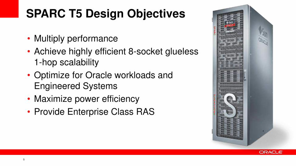
SPARC T5 Design Objectives
• Multiply performance
• Achieve highly efficient 8-socket glueless
1-hop scalability
• Optimize for Oracle workloads and
Engineered Systems
• Maximize power efficiency
• Provide Enterprise Class RAS
6
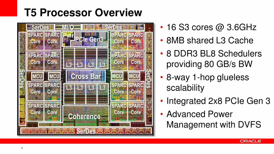
T5 Processor Overview
• 16 S3 cores @ 3.6GHz
• 8MB shared L3 Cache
• 8 DDR3 BL8 Schedulers providing 80 GB/s BW
• 8-way 1-hop glueless
scalability
• Integrated 2x8 PCIe Gen 3
• Advanced Power
Management with DVFS
SPARC
Core
SPARC
Core
SPARC
Core
SPARC
Core
SPARC
Core
SPARC
Core
SPARC
Core
SPARC
Core
SPARC
Core
SPARC
Core
SPARC
Core
SPARC
Core
SPARC
Core
SPARC
Core
SPARC
Core
SPARC
Core
Cross Bar MCU
Coherence
L3 L3 L3 L3
L3 L3 L3 L3
SerDes
SerDes SerDes MI/O
SerD
es
SerD
es
MCU MCU MCU
PCIe Gen3 Pwr
7
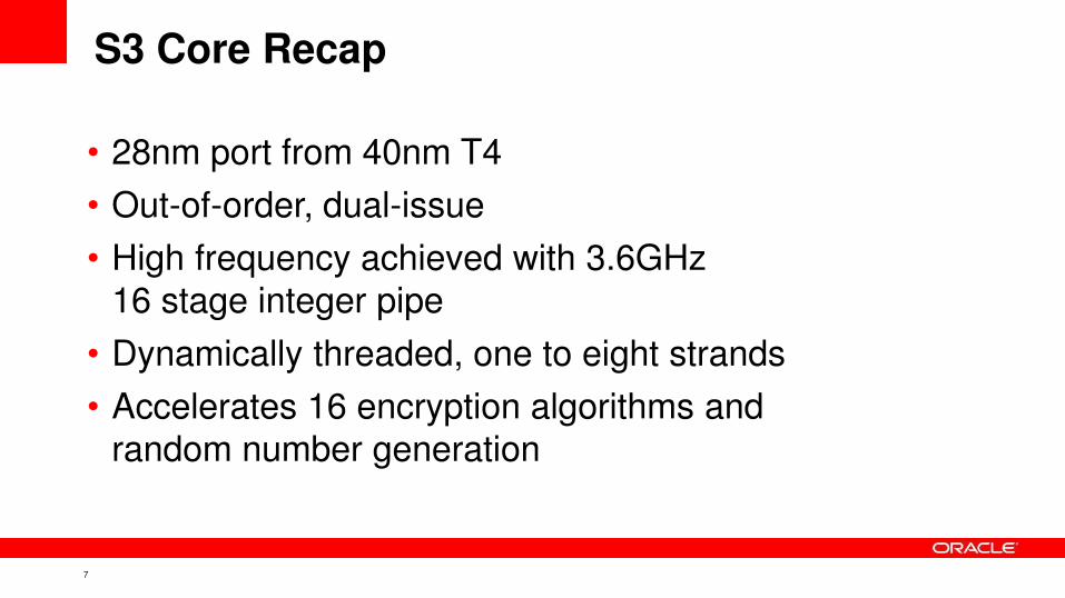
S3 Core Recap
• 28nm port from 40nm T4
• Out-of-order, dual-issue
• High frequency achieved with 3.6GHz
16 stage integer pipe
• Dynamically threaded, one to eight strands
• Accelerates 16 encryption algorithms and
random number generation
8
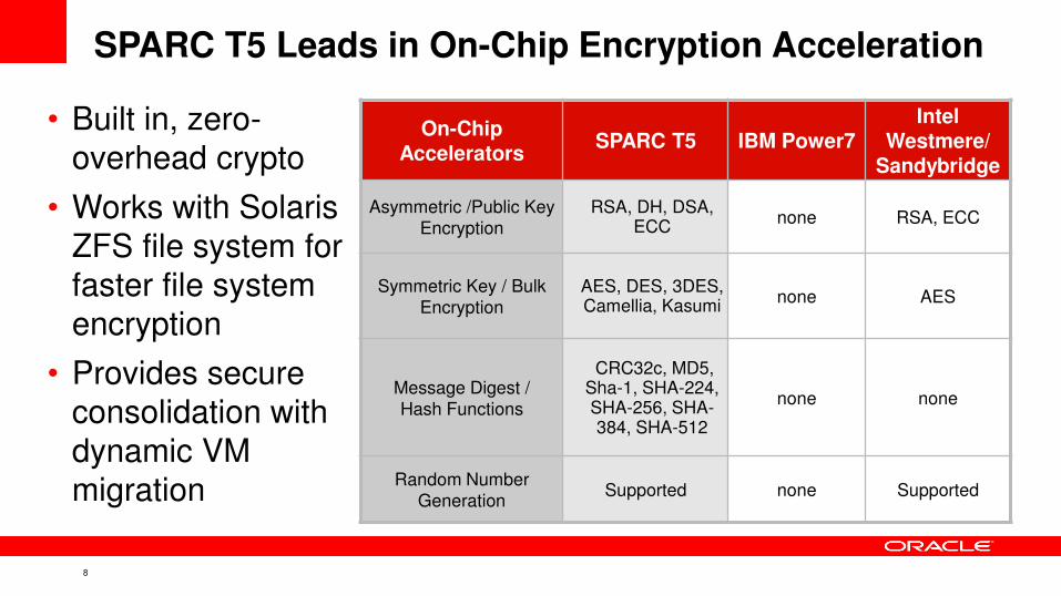
SPARC T5 Leads in On-Chip Encryption Acceleration
• Built in, zero-
overhead crypto
• Works with Solaris
ZFS file system for
faster file system
encryption
• Provides secure
consolidation with
dynamic VM
migration
On-Chip Accelerators
SPARC T5 IBM Power7 Intel
Westmere/ Sandybridge
Asymmetric /Public Key
Encryption RSA, DH, DSA,
ECC none RSA, ECC
Symmetric Key / Bulk
Encryption AES, DES, 3DES, Camellia, Kasumi
none AES
Message Digest /
Hash Functions
CRC32c, MD5, Sha-1, SHA-224, SHA-256, SHA-384, SHA-512
none none
Random Number
Generation Supported none Supported
9
Outline
• Design Objectives
• SPARC T5 Processor Overview
• Core S3
• Cache Hierarchy Components
• Internode Coherency for 8-Socket Scaling
• Power Management Advances
• PCI-Express Gen3 I/O Subsystem
• Summary
10
Core Caches
• 16 KB 4-way set associative L1 Instruction cache
• 16 KB 4-way set associative write through L1 Data cache
• 128 KB 8-way set associative, unified, inclusive L2 cache
11
L2-L3 Interconnect
• 8x9 Crossbar Switch connects the 16 cores to
– 8 address interleaved address banks and
– an I/O bridge
• The L3-L2 direction contains a control and data network.
– control network provides a heads up for dependent instruction wake-up
– Data network is used to return line fill data and send L3-L2 snoops
• Crossbar network has a bisection BW of 1 TBps, 2x T4
12
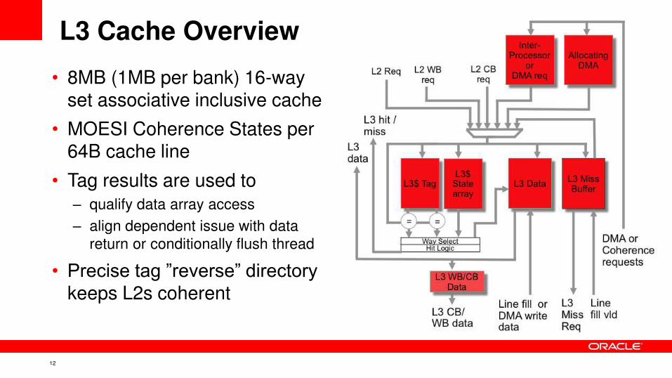
L3 Cache Overview
• 8MB (1MB per bank) 16-way
set associative inclusive cache
• MOESI Coherence States per 64B cache line
• Tag results are used to
– qualify data array access
– align dependent issue with data
return or conditionally flush thread
• Precise tag ”reverse” directory keeps L2s coherent
13
L3 Cache Overview (continued)
• Speeds up IO by allocating DMA buffers in the cache
– Enhances clustered application performance
• Acceleration of contended locks
– L3 forms a chain of same address requests
– Processes them atomically on receiving an exclusive copy
• Supports coherent flushing and retirement of cache
lines to avoid persistent errors
14
Outline
• Design Objectives
• SPARC T5 Processor Overview
• Core S3
• Cache Hierarchy Components
• Internode Coherency for 8-Socket Scaling
• Power Management Advances
• PCI-Express Gen3 I/O Subsystem
• Summary
15
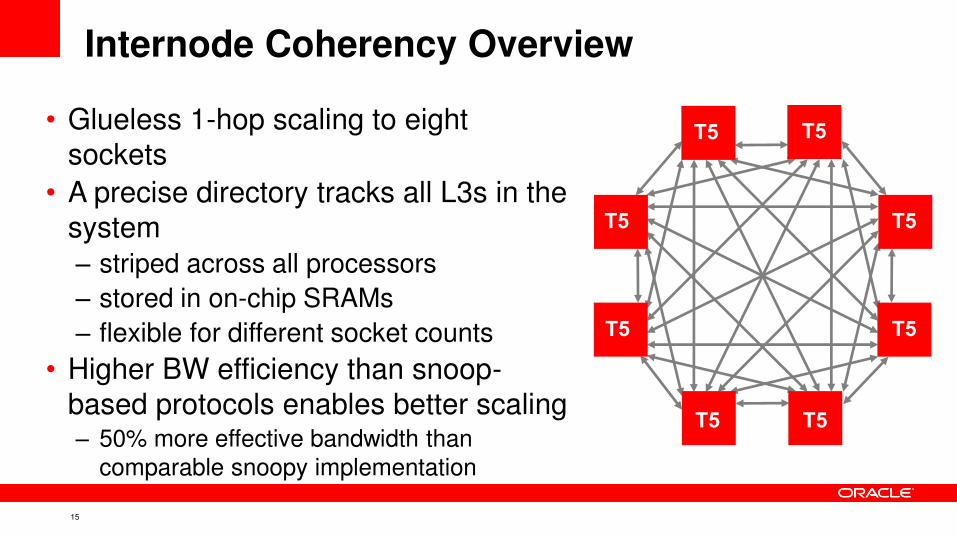
Internode Coherency Overview
• Glueless 1-hop scaling to eight
sockets
• A precise directory tracks all L3s in the
system
– striped across all processors
– stored in on-chip SRAMs
– flexible for different socket counts
• Higher BW efficiency than snoop-
based protocols enables better scaling – 50% more effective bandwidth than
comparable snoopy implementation
T-
T5 T5
T5 T5
T5 T5
T5 T5
16
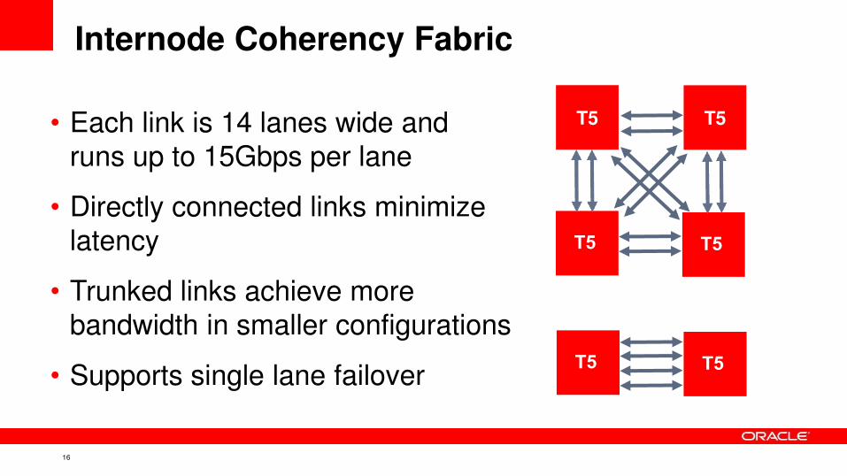
Internode Coherency Fabric
• Each link is 14 lanes wide and
runs up to 15Gbps per lane
• Directly connected links minimize
latency
• Trunked links achieve more
bandwidth in smaller configurations
• Supports single lane failover T5 T5
T5 T5
T5 T5
17
Internode Performance Optimizations
• Speculative memory reads prior to cache line
serialization in the directory
• Cache-to-cache line transfers between nodes
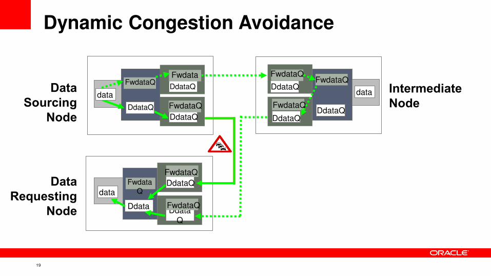
• Dynamic congestion avoidance routes inter-node data
around congested links
18
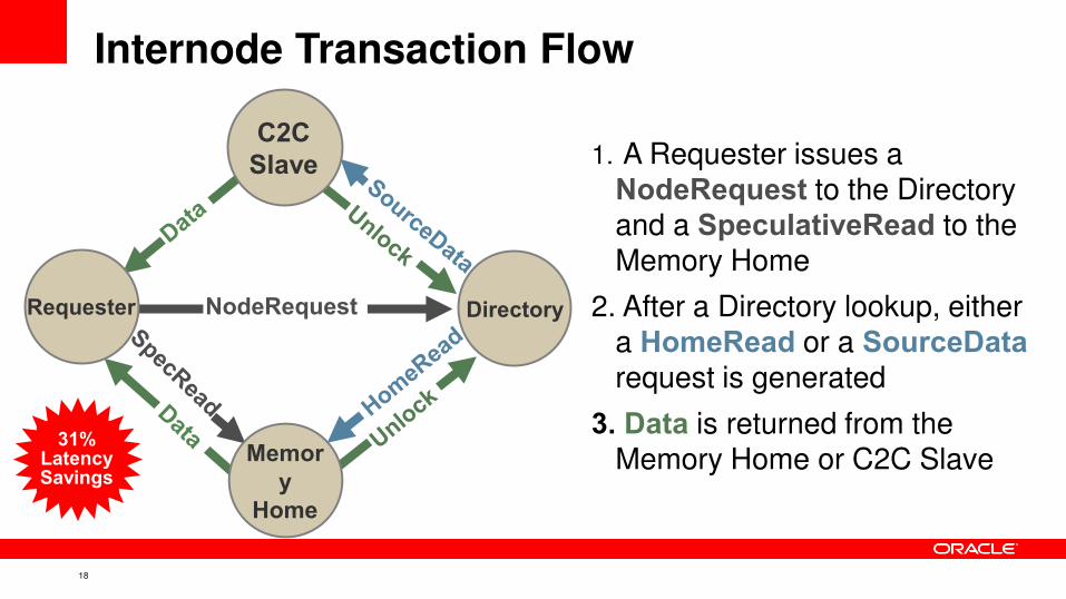
Internode Transaction Flow
1. A Requester issues a NodeRequest to the Directory and a SpeculativeRead to the
Memory Home
2. After a Directory lookup, either a HomeRead or a SourceData request is generated
3. Data is returned from the Memory Home or C2C Slave
31% Latency Savings
Requester Directory NodeRequest
Memor
y
Home
C2C
Slave
19
Dynamic Congestion Avoidance
Data
Sourcing
Node
Intermediate
Node
Data
Requesting
Node
DdataQ
data DdataQ
DdataQ
DdataQ
DdataQ
DdataQ
Ddata
Q
Ddata
DdataQ
data
Fwdata
Fwdata
FwdataQ
FwdataQ
FwdataQ
FwdataQ
Fwdata FwdataQ
data FwdataQ FwdataQ
Fwdata
Q
20
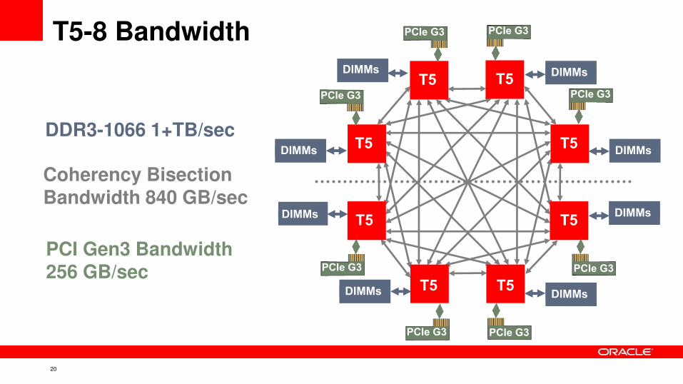
T5-8 Bandwidth
DDR3-1066 1+TB/sec
PCI Gen3 Bandwidth 256 GB/sec
Coherency Bisection Bandwidth 840 GB/sec
T-
T5
DIMMs
DIMMs
DIMMs
DIMMs
DIMMs
DIMMs
DIMMs
DIMMs T5
T5 T5
T5 T5
T5 T5
PCIe G3
PCIe G3
PCIe G3
PCIe G3
PCIe G3
PCIe G3
PCIe G3
PCIe G3
21
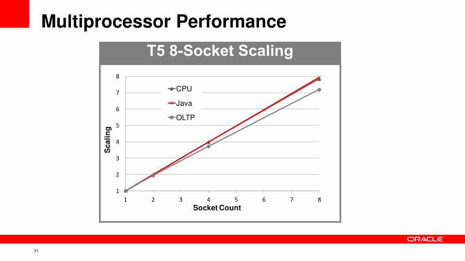
Multiprocessor Performance
1
2
3
4
5
6
7
8
1 2 3 4 5 6 7 8
Scali
ng
Socket Count
CPU
Java
OLTP
T5 8-Socket Scaling
22
Outline
• Design Objectives
• SPARC T5 Processor Overview
• Core S3
• Cache Hierarchy Components
• Internode Coherency for 8-Socket Scaling
• Power Management Advances
• PCI-Express Gen3 I/O Subsystem
• Summary
23
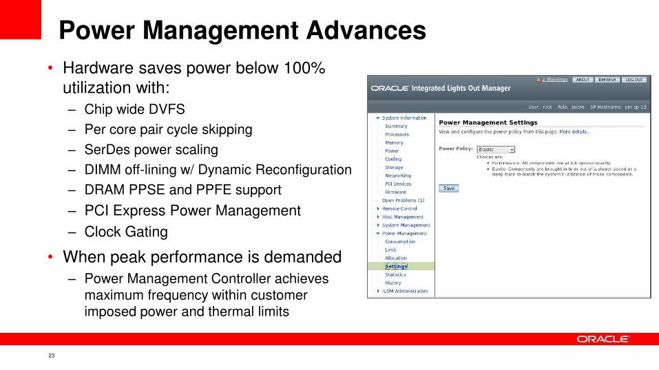
Power Management Advances
• Hardware saves power below 100%
utilization with:
– Chip wide DVFS
– Per core pair cycle skipping
– SerDes power scaling
– DIMM off-lining w/ Dynamic Reconfiguration
– DRAM PPSE and PPFE support
– PCI Express Power Management
– Clock Gating
• When peak performance is demanded
– Power Management Controller achieves
maximum frequency within customer
imposed power and thermal limits
24
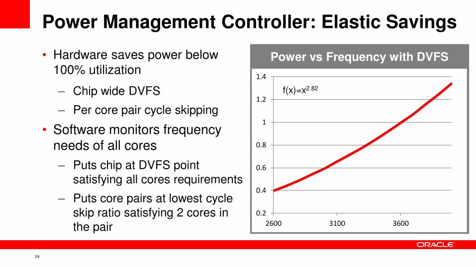
Power vs Frequency with DVFS
Power Management Controller: Elastic Savings
• Hardware saves power below
100% utilization
– Chip wide DVFS
– Per core pair cycle skipping
• Software monitors frequency needs of all cores
– Puts chip at DVFS point satisfying all cores requirements
– Puts core pairs at lowest cycle
skip ratio satisfying 2 cores in the pair
0.2
0.4
0.6
0.8
1
1.2
1.4
2600 3100 3600
f(x)=x2.82
25
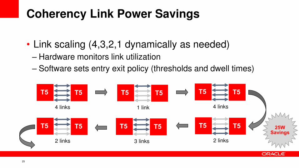
Coherency Link Power Savings
• Link scaling (4,3,2,1 dynamically as needed)
– Hardware monitors link utilization
– Software sets entry exit policy (thresholds and dwell times)
4 links
T5 T5
1 link
T5 T5
3 links
T5 T5
2 links
T5 T5
2 links
T5 T5
4 links
T5 T5
25W Savings
26
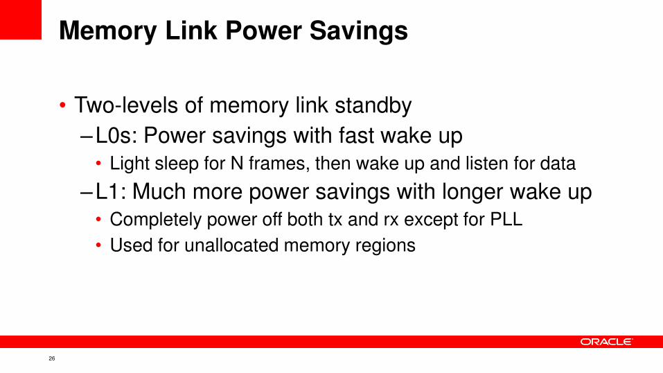
Memory Link Power Savings
• Two-levels of memory link standby
–L0s: Power savings with fast wake up
• Light sleep for N frames, then wake up and listen for data
–L1: Much more power savings with longer wake up
• Completely power off both tx and rx except for PLL
• Used for unallocated memory regions
27
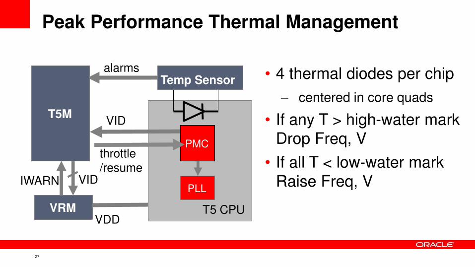
Peak Performance Thermal Management
• 4 thermal diodes per chip
– centered in core quads
• If any T > high-water mark
Drop Freq, V
• If all T < low-water mark
Raise Freq, V
VDD
IWARN
VRM
alarms
VID
throttle
/resume
PLL
T5 CPU
VID
PMC
T5M
Temp Sensor
28
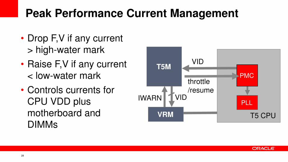
Peak Performance Current Management
• Drop F,V if any current
> high-water mark
• Raise F,V if any current
< low-water mark
• Controls currents for
CPU VDD plus
motherboard and
DIMMs
IWARN
VRM
VID
throttle
/resume
PLL
T5 CPU
VID
PMC
T5M
29
Outline
• Design Objectives
• SPARC T5 Processor Overview
• Core S3
• Cache Hierarchy Components
• Internode Coherency for 8-Socket Scaling
• Power Management Advances
• PCI-Express Gen3 I/O Subsystem
• Summary
30
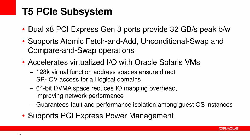
T5 PCIe Subsystem
• Dual x8 PCI Express Gen 3 ports provide 32 GB/s peak b/w
• Supports Atomic Fetch-and-Add, Unconditional-Swap and
Compare-and-Swap operations
• Accelerates virtualized I/O with Oracle Solaris VMs
– 128k virtual function address spaces ensure direct
SR-IOV access for all logical domains
– 64-bit DVMA space reduces IO mapping overhead,
improving network performance
– Guarantees fault and performance isolation among guest OS instances
• Supports PCI Express Power Management
31
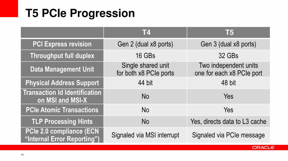
T5 PCIe Progression
T4 T5
PCI Express revision Gen 2 (dual x8 ports) Gen 3 (dual x8 ports)
Throughput full duplex 16 GBs 32 GBs
Data Management Unit Single shared unit
for both x8 PCIe ports Two independent units
one for each x8 PCIe port
Physical Address Support 44 bit 48 bit
Transaction Id Identification on MSI and MSI-X
No Yes
PCIe Atomic Transactions No Yes
TLP Processing Hints No Yes, directs data to L3 cache
PCIe 2.0 compliance (ECN “Internal Error Reporting”) Signaled via MSI interrupt Signaled via PCIe message
32
Outline
• Design Objectives
• SPARC T5 Processor Overview
• Core S3
• Cache Hierarchy Components
• Internode Coherency for 8-Socket Scaling
• Power Management Advances
• PCI-Express Gen3 I/O Subsystem
• Summary
33
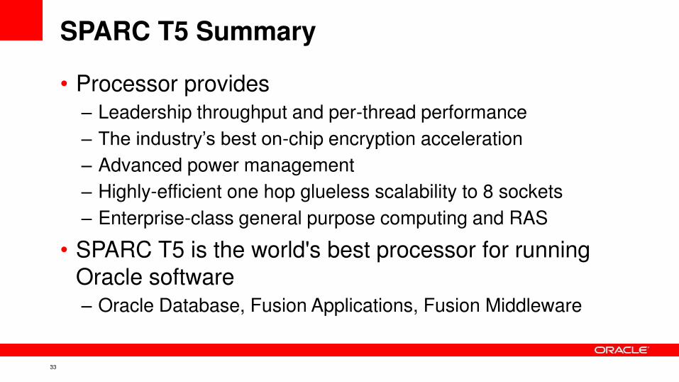
SPARC T5 Summary
• Processor provides
– Leadership throughput and per-thread performance
– The industry’s best on-chip encryption acceleration
– Advanced power management
– Highly-efficient one hop glueless scalability to 8 sockets
– Enterprise-class general purpose computing and RAS
• SPARC T5 is the world's best processor for running
Oracle software
– Oracle Database, Fusion Applications, Fusion Middleware
34
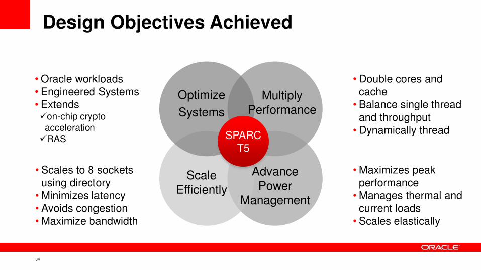
• Scales to 8 sockets
using directory
• Minimizes latency
• Avoids congestion
• Maximize bandwidth
• Double cores and
cache
• Balance single thread
and throughput
• Dynamically thread
• Oracle workloads
• Engineered Systems
• Extends on-chip crypto
acceleration RAS
• Maximizes peak
performance
• Manages thermal and
current loads
• Scales elastically
Optimize
Systems
Multiply
Performance
SPARC
T5
Scale
Efficiently
Advance
Power
Management
Design Objectives Achieved

35
Q&A
36

37