Software Defined S-Band Ground Station Transceiver for ... · PDF filefor Satellite...
77
Diploma Thesis Software Defined S-Band Ground Station Transceiver for Satellite Communications under the supervision of Dipl.-Ing. Michael Fischer and Univ.Prof.Dr. Arpad L. Scholtz Institute of Telecommunications, E389 Department of Electrical Engineering Vienna University of Technology by Alexandra Martínez Torío 1027385 Kandlgasse 30, 1070 Wien Wien, August 2011
Transcript of Software Defined S-Band Ground Station Transceiver for ... · PDF filefor Satellite...

Diploma Thesis
Software DefinedS-Band Ground Station Transceiver
for Satellite Communications
under the supervision of
Dipl.-Ing. Michael Fischer
and
Univ.Prof.Dr. Arpad L. Scholtz
Institute of Telecommunications, E389
Department of Electrical Engineering
Vienna University of Technology
by
Alexandra Martínez Torío1027385
Kandlgasse 30, 1070 Wien
Wien, August 2011

“Do not go where the path may lead,go instead where there is no path and leave a trail.”Ralph Waldo Emerson

Abstract
Satellite communications meant, in the last few decades, a reliably outstandingtechnical advance in different fields such as physics, astrophysics, geography, elec-tronics and communications. It became the most significant tool to ease humanscientific research for both Earth and deep space, whereas it is still giving supportto current commercial services.
The current project deals with the design and construction of a ground stationat the Institute of Telecommunications at the Vienna University of Technologywhich should handle three different low Earth orbiting satellite missions: MOST,COROT and BRITE constellation. They are aimed at the research in the scien-tific areas of the physics, asteroseismology and communications. Communicationis performed at S-band frequencies (2.00 - 2.45 GHz), UHF (435 - 438 MHz) andVHF (144 - 146 MHz).
This thesis is focused on the design and characterization of a front-end for thisground station by means of Software Defined Radio, using an USRP1 by Ettusas the main hardware component for up- and downconversion and analog-digitalconversion. The digital output is treated by the software tool GNU Radio. Payingspecial attention to the hardware employed and the modulation and demodula-tion block’s performance at the graphical software interface, a detailed studyof the complete system is carried out and the fundamentals for the prospectiveadaptation procedure for both hardware and software blocks to the final projectmission requirements, are consequently determined.
Resumen
En las últimas décadas, las comunicaciones por satélite han supuesto un granavance técnico fiable en sectores como la física, astrofísica, geografía, electrónicay comunicaciones; llegando así a ser una herramienta importante que facilita eldesarrollo científico tanto en la Tierra como en el espacio, a la vez que prestanotros servicios comerciales del día a día.
El proyecto que se está llevando a cabo, está centrado en el diseño y construcciónde una estación terrestre en el Instituto de Telecomunicación de la Universi-dad Técnica de Viena, la cual soportará tres misiones de satélites LEO: MOST,
iii

COROT y la constelación BRITE. Mediante enlaces en banda S (2.00 - 2.45 GHz),UHF (435 - 438 MHz) y VHF (144 - 146 MHz), el objetivo final de esta comuni-cación es la investigación científico-educacional en el área de la física, asteroseis-mología y de las comunicaciones.
Concretamente esta tesis se centra en el diseño y caracterización del terminal dedicha estación terrestre a través de Software Defined Radio, usando una USRP1como hardware básico para la conversión en frecuencia y para la conversiónanalógico-digital. La salida digital es tratada a través de una herramienta soft-ware propiedad de GNU Radio. Prestando especial atención a los componentesdel hardware y al funcionamiento de los bloques de modulación y demodulaciónen la interfaz gráfica del software empleado, se lleva a cabo un estudio detalladodel sistema completo, determinando así, las bases fundamentales para el posteriorproceso de adaptación tanto de software como hardware para así satisfacer losrequisitos establecidos por los satélites de dicho proyecto.
iv

Contents
1 Introduction 1
2 MOST, COROT and BRITE 42.1 Missions and Motivation . . . . . . . . . . . . . . . . . . . . . . . 42.2 Project Basic Requirements . . . . . . . . . . . . . . . . . . . . . 5
2.2.1 Frequency Ranges . . . . . . . . . . . . . . . . . . . . . . . 52.2.2 Equivalent Isotropically Radiated Power Values . . . . . . 52.2.3 Power Density . . . . . . . . . . . . . . . . . . . . . . . . . 62.2.4 Data Rate . . . . . . . . . . . . . . . . . . . . . . . . . . . 62.2.5 Modulation Standards . . . . . . . . . . . . . . . . . . . . 72.2.6 Other Parameters . . . . . . . . . . . . . . . . . . . . . . . 7
3 Ground Station 93.1 Background Project . . . . . . . . . . . . . . . . . . . . . . . . . . 93.2 A Software Defined Ground Station . . . . . . . . . . . . . . . . . 9
4 Hardware 154.1 Motherboard . . . . . . . . . . . . . . . . . . . . . . . . . . . . . 15
4.1.1 Block Diagram Description . . . . . . . . . . . . . . . . . . 154.1.2 Analog-to-Digital and Digital-to-Analog Converters . . . . 164.1.3 Clock Distribution . . . . . . . . . . . . . . . . . . . . . . 174.1.4 Field Programmable Gate Array . . . . . . . . . . . . . . . 17
4.2 Daughterboard “RFX2400” . . . . . . . . . . . . . . . . . . . . . . 194.2.1 Receiver Components . . . . . . . . . . . . . . . . . . . . . 204.2.2 Transmitter Components . . . . . . . . . . . . . . . . . . . 21
4.3 Auxiliary Ports . . . . . . . . . . . . . . . . . . . . . . . . . . . . 22
5 GNU Radio Companion Blocks 235.1 Reception Path . . . . . . . . . . . . . . . . . . . . . . . . . . . . 24
5.1.1 Measurement Setup . . . . . . . . . . . . . . . . . . . . . . 245.1.2 DPSK Demodulator . . . . . . . . . . . . . . . . . . . . . 25
5.2 Transmission Path . . . . . . . . . . . . . . . . . . . . . . . . . . 335.2.1 Measurement Setup . . . . . . . . . . . . . . . . . . . . . . 335.2.2 DPSK Modulator . . . . . . . . . . . . . . . . . . . . . . . 34
6 The QPSK Test Signals 386.1 Reception Path . . . . . . . . . . . . . . . . . . . . . . . . . . . . 38
v

Contents
6.1.1 Frequency and Power Level . . . . . . . . . . . . . . . . . 386.1.2 Modulation and Standards . . . . . . . . . . . . . . . . . . 38
6.2 Transmission Path . . . . . . . . . . . . . . . . . . . . . . . . . . 406.2.1 Frequency and Power Level . . . . . . . . . . . . . . . . . 416.2.2 Modulation and Standards . . . . . . . . . . . . . . . . . . 41
7 Measurements 437.1 Receiver . . . . . . . . . . . . . . . . . . . . . . . . . . . . . . . . 43
7.1.1 Frequency Response . . . . . . . . . . . . . . . . . . . . . 437.1.2 Dynamic Range and Attenuation Response . . . . . . . . . 447.1.3 Compression Point . . . . . . . . . . . . . . . . . . . . . . 457.1.4 Third Order Intercept Point . . . . . . . . . . . . . . . . . 467.1.5 Bit Error Rate vs Input Power Level . . . . . . . . . . . . 487.1.6 Error Distribution . . . . . . . . . . . . . . . . . . . . . . 49
7.2 Transmitter . . . . . . . . . . . . . . . . . . . . . . . . . . . . . . 517.2.1 Frequency Response . . . . . . . . . . . . . . . . . . . . . 527.2.2 Error Vector Magnitude . . . . . . . . . . . . . . . . . . . 53
7.3 Communication Example . . . . . . . . . . . . . . . . . . . . . . . 547.3.1 Reception Example . . . . . . . . . . . . . . . . . . . . . . 547.3.2 Transmission Example . . . . . . . . . . . . . . . . . . . . 58
8 Conclusions 61
Acknowledgments 63
Bibliography 64
List of Abbreviations and Symbols 67
List of Figures 69
List of Tables 71
vi

Chapter 1
Introduction
Since the Second World War II very different technologies were expanded, likemissiles and microwaves. And the combination of both of them brought to lifea new era, the era of a new form of communication, complementing the alreadyexisting ground radio-cabled networks, providing bigger ranges, capacities andaccess to areas that would not be possible by any other technology. Satellitecommunications era started with the launching of the Soviet Sputnik I, the firstartificial satellite working on 20.005 and 40.002 MHz, on October 4, 1957. Then,in 1962, AT&T launched Telstar, the world’s first true communications satellite.After that, innumerable satellites have been set into orbit supporting any kindof applications [1].
The use of satellites came up to fulfill the need of encountering difficulties dueto the congestion and low reliability on long distance cable networks, such astransoceanic routes, and they also provide a more advantageous communicationcompared to the cabled links [2]:
- they support point-to-multipoint communication;- they handle longer links without increasing the cost of the service;- they reach remote areas where it would be impossible to supply any service
with terrestrial routes and mobile terminals such as ships, aircrafts, etc;- they offer bigger channel capacities.
Any satellite communication is divided into space and ground segment as it canbe seen in Figure 1.1. The space segment is purely constituted by the artificialsatellites which are categorized depending on the orbit they are set into. Depend-ing on the altitude, they are classified into LEO1 satellites, MEO2 satellites, etc.Regarding the trajectory described, the classification is into elliptical inclined or-bit, polar orbit or circular equatorial orbit. The last type of satellites also knownas GEO3 satellites, have an equatorial orbit and their speed and direction makethem to be stationary relative to the Earth. But not only satellites define thespace segment, but also its on-board equipment and the telemetry, tracking andcontrol system.
1Low Earth Orbit2Medium Earth Orbit3Geostationary Earth Orbit
1

1 Introduction
The Earth or ground segment consists of the ground terminals and its equip-ment such as antennas, electronics and links to the service terrestrial networks.They can be fixed ground stations or can be mobile devices.
Figure 1.1: Satellite communications basic scenario [3].
This thesis describes a part of an ongoing project in satellite communicationsto build a ground station at the Institute of Telecommunication at the ViennaUniversity of Technology, using a software defined radio basis. The predefinedobjective is to get to know the hardware in detail and get deep into the softwareperformance of this front-end, so that a complete understanding of the systemand the signal treatment can be reached and the future steps can be clarified, inorder to set this front-end up and make it run for the missions considered in thisproject.
Hence, Chapter 2 describes the three different satellite missions – motivationof the project – with their own satellite segments parameters to which we wantto finally adapt our system. The common ground segment and its main featuresis given in Chapter 3.
In Chapter 4, there is a detailed description of the hardware employed for themixer, the different components on it and their functional contribution to themain goal. Meanwhile, the performance of the software running in the PC isanalyzed in Chapter 5, paying special attention to the modulation and demodu-lation blocks.
In order to get a proper understanding of the signal behavior along the sys-tem, Chapter 6 describes the signal flow, followed by Chapter 7, where it comesto a detailed characterization of the whole system and the explanation to theencountered anomalies.
And finally, in Chapter 8, the conclusions are seen and, as a complementary
2

1 Introduction
work, the future steps and objectives are established, based on the research ofthis thesis, in order to follow up with this project and achieve the desired goals.
3

Chapter 2
MOST, COROT and BRITE
2.1 Missions and Motivation
Every satellite communication is held by two segments: the space segment andthe Earth segment. The space segment is basically constituted by the artificialsatellite constellations.
The space astronomy missions which give incentive to this project are handledin three different satellite constellations: MOST, COROT and BRITE.
MOST: Under the acronym MOST stands the project Microvariability andOscillations of STars. It is a microsatellite space telescope mission led bythe Canadian Space Agency.The MOST satellite is a LEO satellite with an orbital period of 100 min,which handles the study of asteroseismology and its mission is to measurethe brightness variations in the stars during a 60-day period, to find outthe age of the stars and to discover exoplanets, in order to get to know theUniverse’s origin [4], [5].Our ground station on the roof of the Electrical Engineering building of theVienna University of Technology is planned to be one of the four groundstations working with this satellite, together with another ground stationin Vienna placed at the Institute of Astronomy and two more in Canada(Vancouver and Toronto).
COROT: COnvection ROtation and planetary Transits is the name of a missionconducted by the CNES, Centre National d’Études Spatiales and ESA,European Space Agency.Its mission consists of the search for exoplanets by detecting the stars’ lightfade out as the exoplanet cuts in front of the stars, and the calculation ofthe stars’ mass, age and chemical composition by means of asteroseismology[6], [7].The Earth segment is placed in different geographical areas around theworld. Our Vienna ground station also works as a secondary station forCOROT [4], [5].
BRITE: In order to explore massive luminous stars, which dominate the ecol-ogy of the Universe, by means of a precise differential photometry and
4
Chapter 2 MOST, COROT and BRITE
asteroseismology, the BRIght Target Explorer Constellation mission willbe carried out.A constellation of four nearly identical Austrian/Canadian LEO nanosatel-lites will allow a longer duty cycle of observation compared to the case ofhaving just one satellite. These are grouped in pairs in which each satellitefilters different spectral ranges, so that an spectral improvement is achieved.Different pairs of satellites are planned to be placed in different orbits [5].It is to mention, that the first Austrian satellite TUGSAT-1/BRITE-Austriafunded by the Austrian Space Program forms part of this mission [8], [9].The communication with our ground station will be full duplex.
2.2 Project Basic Requirements
In this subsection, a list of the main parameters of the different satellite constel-lations which make up the space segment of this project is given [4], [5], [8], [9].These parameters must be taken into account as requirements for our groundstation design and configuration.
2.2.1 Frequency Ranges
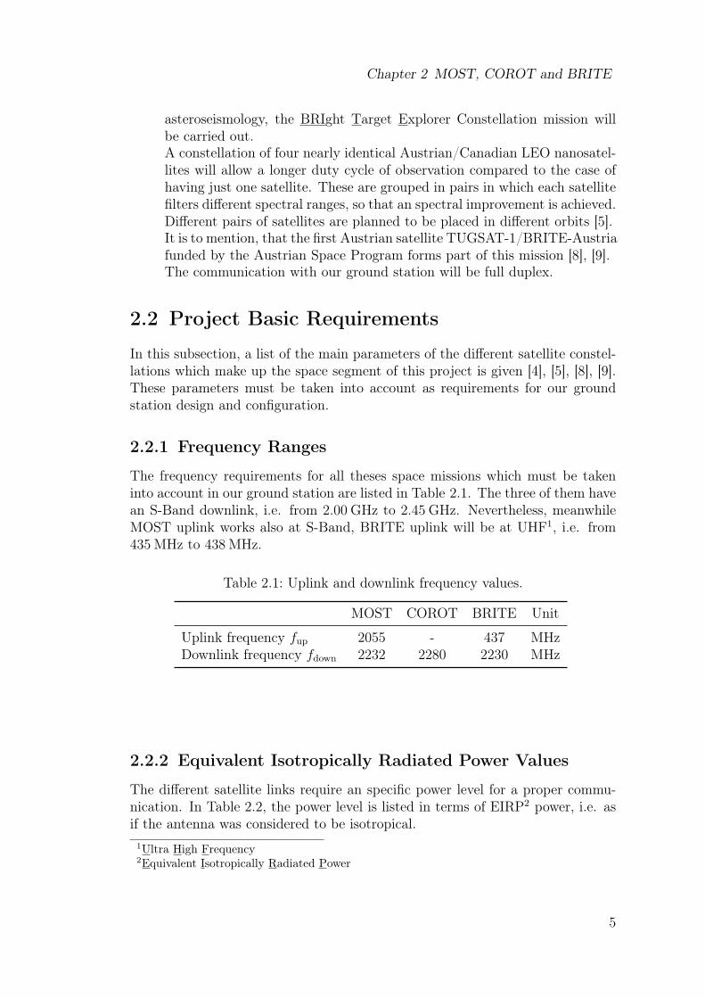
The frequency requirements for all theses space missions which must be takeninto account in our ground station are listed in Table 2.1. The three of them havean S-Band downlink, i.e. from 2.00 GHz to 2.45 GHz. Nevertheless, meanwhileMOST uplink works also at S-Band, BRITE uplink will be at UHF1, i.e. from435 MHz to 438 MHz.
Table 2.1: Uplink and downlink frequency values.
MOST COROT BRITE Unit
Uplink frequency fup 2055 - 437 MHzDownlink frequency fdown 2232 2280 2230 MHz
2.2.2 Equivalent Isotropically Radiated Power Values
The different satellite links require an specific power level for a proper commu-nication. In Table 2.2, the power level is listed in terms of EIRP2 power, i.e. asif the antenna was considered to be isotropical.
1Ultra High Frequency2Equivalent Isotropically Radiated Power
5

Chapter 2 MOST, COROT and BRITE
Table 2.2: Uplink and downlink power (EIRP) levels.
MOSTuplink MOSTdownlink COROT BRITEuplink BRITEdownlink Unit
69.5 25 37.7 50 27 dBm39.5 −5 7.7 20 −3 dBW
8912.5 0.32 5.85 100 0.5 W
2.2.3 Power Density
Another way to express the power requirements is as the power density. Incontrast with the power level, which is the power radiated in the link bandwidth,the power density is the power per 1 Hz. These values are shown in Table 2.3.
Table 2.3: Uplink and downlink power densities.
MOST COROT BRITE Unit
Uplink EIRP Pup −10.9 −25.4 dBW/HzDownlink EIRP Pdown −55.3 −60 dBW/Hz
2.2.4 Data Rate
The amount of data processed or conveyed per second for all the satellite links isshown in Table 2.4.
Table 2.4: Uplink and downlink data rates.
MOST COROT BRITE Unit
Uplink Rate Rup 9.6 4 kbpsDownlink Rate Rdown 38.4 838.9 32 to 256 kbps
6

Chapter 2 MOST, COROT and BRITE
2.2.5 Modulation Standards
The information needs to be modulated in order to be transmitted. The modu-lation standards (Table 2.5) employed by the different satellite missions, whichdoes not coincide in both uplink and downlink paths for the same satellite, canbe a GFSK3, QPSK4 or BPSK5. The only difference between them lays in theparameter of the carrier signal which holds the information, i.e. the frequencyfor FSK6 or the phase for PSK7.
Table 2.5: Uplink and downlink modulation standards.
MOST COROT BRITE
Uplink GFSK GFSKDownlink BPSK QPSK BPSK
2.2.6 Other Parameters
Other requirements of the three missions are the bandwidth BW and the band-width including the Doppler shift. In case of MOST, it uses also alternative fre-quencies for up- and downlink. The polarization can be linear (LP8) or circular,in this last case it can be right hand (RHCP9) or left hand circular polarization(LHCP10). All the parameters are shown in Table 2.6.
3Gaussian Frequency Shift Keying4Quadrature Phase Shift Keying5Binary Phase Shift Keying6Frequency Shift Keying7Phase Shift Keying8Linear Polarization9Right Handed Circular Polarization
10Left Handed Circular Polarization
7

Chapter 2 MOST, COROT and BRITE
Table 2.6: Other parameters of the satellite missions.
BW11 BW + Doppler Alternative Freq Polarization
Unit kHz kHz MHz -MOSTup 110 2045.9 RHCP
MOSTdown 2231.6 RHCPCOROT 2000 270 - RHCP&LHCP
BRITEupl 35 35 - LPBRITEdown 500 500 - LP
8

Chapter 3
Ground Station
A ground station can be defined as a group of components which performs anuplink and/or downlink path in order to establish a communication channel witha satellite. These components are basically an antenna, the element that radiatesand receives the radio waves; the tracking and the rotator, that takes care ofdetermining where the satellite is and helps the antenna to point towards it; atransmitter, which modulates, converts and amplifies the signal to be transmitted;the receiver, that takes the received signal from the satellite and demodulates itafter amplifying it; and last but not least, the power supply to provide the powerto make the other components work [3].
To establish a communication channel from a ground station to a satellite,information about the position and velocity of the satellite is required in orderto design the ground station equipment and structure. Outgoing from the in-formation about the MOST, COROT and BRITE missions in Chapter 2, thespecifications for the needed ground station are defined [4].
This chapter will describe the Earth or ground segment of this satellite com-munication project.
3.1 Background Project
As a previous project, the Vienna Ground Station (VGS) was built to fulfill theMOST mission. This ground station uses separated antennas for uplink anddownlink in order to mitigate crosstalk and to achieve an optimized downlinkperformance. At the downlink the signal is taken by a parabolic dish, while theuplink signal is radiated by a Yagi antenna group [4].
The core of the present project is located at the Institute of Telecommunica-tions, Vienna University of Technology.
3.2 A Software Defined Ground Station
The general components of a ground station are shown in the Figure 3.1 [3].
9

Chapter 3 Ground Station
Feeding Block [3]:
- Antenna: It sends the signal to the satellite and receives the one comingfrom the satellite. The antenna in our ground station is a 3.7 m dish.
- Duplexer: Element which allows to have a duplex communication using asingle antenna.
- LNA1 and power amplifier: The low-noise amplifier performs the amplifi-cation of weak received signals, and the power amplifier does the samewith the transmitted signals in order to reach the power level necessary.
USRP:
- Downconverter and upconverter: These elements take care of shifting thefrequency of the S-Band signal received to an IF2 and viceversa for thetransmitted signal. This function is done by the USRP3 (Figure 3.2), acomputer-hosted hardware developed by Ettus for allowing general pur-pose computers to work out as a software radio, using a daughterboard(Figure 3.3) specifically design for a certain bandwidth connected to themotherboard (Figure 3.4). This element includes the digital-analog con-verters, ADC4 and DAC5. In general terms, it serves as digital basebandand IF section for our ground station. This device will be on greater detailin Chapter 4 [10], [11].
PC:
In contrast to other radio communication systems, this ground station is aSoftware Defined Radio Station, where most of the components (e.g modu-lator, demodulator, coder, decoder, etc.), instead of being implemented inhardware, they are performed by means of a software on a personal com-puter. The software development toolkit chosen for this project is GNURadio which includes a user-friendly graphical interface called GRC6.- Demodulator and modulator: To demodulate and modulate the signals
at the intermediate frequency. It is usually performed by a modem.- Decoder and coder: The coding and decoding of the signals is usually
executed by a TNC7, a device which integrates the higher protocollayers, e.g. the AX.25 protocol [5].
The fact of using a certain open-source software instead of a dedicated TNC
2Intermediate Frequency3Universal Software Radio Peripheral4Analog-to-Digital Converter5Digital-to-Analog Converter6GNU Radio Companion7Terminal Node Controller
10

Chapter 3 Ground Station
or a modem, and combined with the flexible hardware provided by Ettuspermits a rapidly evolving platform for radio communication.
11

Chapter 3 Ground Station
Figure 3.1: Ground station diagram.
12

Chapter 3 Ground Station
Figure 3.2: Universal Software Radio Peripheral.
Figure 3.3: RFX2400 Daughterboard.
13

Chapter 3 Ground Station
Figure 3.4: USRP1 Motherboard.
14

Chapter 4
Hardware
The USRP offered by Ettus Research LLC, a subsidiary of National Instruments,is a hardware – working as the digital baseband and IF section of a radio groundstation – specifically designed to let simple general purpose personal computersor embedded computing devices to operate as a high bandwidth software radio.It performs the digital up and down conversion, decimation and interpolation,which are done in a high speed FPGA1 and the frequency shifting, in a specificdaughterboard depending on the application needs [11]. The intended purpose isto leave the signal processing, modulation and demodulation to be done on thehost computer, that it is connected through a high-speed USB link.
4.1 Motherboard
4.1.1 Block Diagram Description
The USRP used, the version 1, has 4 high-speed ADCs, each of them samplingat 64 Msamples/s and generating 12 bits/sample. There are also 4 DACs, work-ing at 128 Msamples/s and 14 bits/sample. Those are also the 4 inputs and 4outputs to an Altera Cyclone EPIC12 FPGA [12]. The FPGA is connected tothe Cypress FX2 USB2 Controller in order to connect through a high-speed USB2.0 interface with the computer [11]. The Figure 4.1 presents a block diagram ofthe motherboard of the USRP 1, and it is to say that the blue arrows representthe flux of data between the elements and the red ones the control signalling orauxiliary channels.
For the reception path, the received analog data comes from the daughter-boards where it was downconverted in frequency to IF and then it is convertedto digital domain in order to get into the FPGA and as the last step to leavethe USRP through the USB interface. On the other hand, for the transmissionpath, the digital signal coming from the computer gets into the FPGA and thenthe analog signal is constructed and it is shifted up in frequency in the daugh-terboards in order to be radiated. The performance of the different blocks willbe explained in the following sections [11], [13].
1Field Programmable Gate Array2Universal Serial Bus
15

Chapter 4 Hardware
Figure 4.1: USRP block diagram. Blue arrows are information flow and red ar-rows control signalling flow [11].
4.1.2 Analog-to-Digital and Digital-to-Analog Converters
At the reception path, there are 4 high-speed 12-bit ADCs, with a samplingrate of 64 MHz. Considering Nyquist’s theorem, a band as wide as 32 MHz canbe digitalized [11], [14]. The ADC uses bandpass-sample signals up to around200 MHz or even more if some decibels of loss is permitted [15]. Any time weare sampling signals which frequency, i.e. IF, is larger than 32 MHz, there willbe aliasing. Even though, we can sample signals at higher frequency as far as
16
Chapter 4 Hardware
the band of interest is not being degraded and keeping in mind that this band isgoing to be mapped somewhere between −32 MHz and 32 MHz. The higher theIF is, the more the SNR3 is spoiled by jitter. The recommended value for this IFis around 100 MHz [11].
There are also 4 high-speed 14-bit DACs for the transmition path. Here theclock used is at 128 MHz, so here Nyquist limit is set at 64 MHz [14]. For thereconstruction of the signal it is necessary to filter under this Nyquist limit [15].
4.1.3 Clock Distribution
As we are working with a synchronous digital system, one important section ofthe system is the clock distribution network or the clock tree. This networkdistributes the clock signal to the elements in the system that need it, in orderto define a time reference for the routing of data within the system.
In this particular system, the master clock signal is generated by a VoltageControlled Temperature Compensated Crystal Oscillator (VCTCXO4) of 64 MHz[16]. This signal, before being fed into the distribution network, can be modifiedin frequency, in order to get other clock frequencies [17], the 800 MHz ClockDistribution Divider AD9513 provides us with 3 different output clock signalswhich frequency is resulting from the division of the master clock frequency by aninteger factor and with a certain phase offset and delay compared to the masterclock. The current logical configuration of the motherboard clock distributionsection provides a non-divided signal clock in a bypass configuration at the threeoutputs, i.e. a 64 MHz signal [18]. Then, this signal not only governs the timereference in the FPGA but also reaches the daughterboards, in order to have auniversal common reference.
This clock signal is necessary for the VCO5 at the daughterboard. Neverthe-less, there is also the possibility to have an independent crystal oscillator at thedaughterboard instead of using the same time reference as in the motherboard[19].
4.1.4 Field Programmable Gate Array
A FPGA is an integrated circuit that can be configured or programmed using ahardware description language by the customer. They can implement any logicalfunction which can be performed by an application-specific integrated circuit [20].In our USRP, the FPGA holds the task to carry out high bandwidth math andadapt the data rate coming from the ADC to the one that can flow throughthe USB link, and the other way round. This block is directly connected to theUSB interface microcontroller – the Cypress FX2 [17]. The FPGA runs four
3Signal to Noise Ratio4Voltage Controlled Temperature Compensated Crystal Oscillator5Voltage Controlled Oscillator
17

Chapter 4 Hardware
DDC6s. Those converters are implemented with some stage CIC7 filters for addsand delays and 31 taps halfband filters placed in cascade with the CIC filters forthe spectral shaping and the rejection of signals out of band. For the transmitionpath, the two DUC8s are not included in the FPGA but only their CIC filters[11].
Digital Down Converter
The DDC downconverts the signal from the IF frequency to the baseband, mul-tiplying the input signal by a constant frequency generated from an NCO9 [11].
Then, the signal is decimated in order to adapt the data rate to the USB 2.0bounds of 32 MBytes/s. As the input signal is a complex signal at IF, sampledat a rate of 64 MHz, the output is still a complex signal centered at 0 Hz anddecimated with a factor N . The decimation procedure consists of a low-passfilter which selects the frequency band ranging from −Fs/N to Fs/N and a downsampler, to spread the spectrum to the new sampling frequency F ′
s = Fs/N .The decimation factor ranges from 8 to 256 [11]. The samples leaving the USBinterface are in 16-bit integers IQ format, which gives a value of 4 Bytes percomplex sample. If we have the full capacity of the USB link at our disposal, thehighest new sampling rate across the USB is 8 Msamples/s [11].
F ′s =
32 MBytes/s4 Bytes/sample
= 8 Msamples/s (4.1)
The decimation factor can be easily calculated as
F ′s =
Fs
N→ N =
Fs
F ′s
=64 MHz8 MHz
= 8. (4.2)
In case the full capacity of the USB is not needed, we would just need to increasethe decimation factor, to achieve lower sampling rates.
Figure 4.2 represents a simple scheme of the FPGA DDC.
Digital Up Converter
This block converts a baseband IQ sampled signal coming from the USB path tothe IF. This is proceeded in two steps, the first is complex multiplication with asignal generated by a fine NCO and a second coarse multiplication with a signalcoming from another NCO [11]. At the end the output signal is at the IF.
In between the two complex multiplications an interpolation is done with aprogrammable interpolation rate L, in order to restore the sampling rate used at
6Digital Down Converter7Cascaded Integrator-Comb8Digital Up Converter9Numerical-Controlled Oscillator
18

Chapter 4 Hardware
Figure 4.2: FPGA digital down converter [11]. Since the decimation is performedin two steps, the Ntotal=2N.
the DACs (128 MHz). It can be just seen as the reverse process of the DDC. Theinterpolation filters are two, first a 39-tap LPF10 followed by a 15-tap one [11].
In contrast to the DDC, the DUC is not performed by the FPGA but by aAD9862 CODEC chip [15], only the CIC interpolators are included in the FPGA.
Figure 4.3 represents the scheme of the USRP DUC.It is important to mention that the USB link allows full duplex mode, so the
maximum capacity of 32 MBytes/s is available for both paths.
4.2 Daughterboard “RFX2400”
For the analog down and up conversion in frequency, from and to IF, a daughter-board is needed, turning a USRP motherboard into a complete RF transceiversystem. The selection of the daughterboard depends on the frequency neces-sary for our application, power specifications, signal to noise requirements or ifwe need a MIMO11 capable board. There are simple boards for transmission orreception, but also transceiver boards [21].
10Low-Pass Filter11Multiple Input Multiple Output
19

Chapter 4 Hardware
Figure 4.3: USRP digital up converter [11].
The election of the board “RFX2400” lays basically on the need of a transceiverboard to work close to the spectral band ranging from 2 GHz to approximately2.5 GHz established by the three mission frequency requirements. The transmit-ted power is 50 mW typically and uses synthesizers for independent transmissionand reception frequencies, which are in the band from 2.3 GHz to 2.9 GHz. Theboard “RFX2200” also works around the frequency band needed but in a narrowerwindow so it does not cover all of them, only from 2 GHz to 2.4 GHz [21].
Analyzing either the “RFX2400” frequency response, dynamic range (sensitivityand saturation point) or any other behaviors, is the first step to get to know thisboard, checking how good it is for our purposes and how it can be adapted to fulfillour expectations (Chapter 7). The next sections are focused on the descriptionof the receiver and transmitter components of the “RFX2400”.
4.2.1 Receiver Components
Since there are two reception ports on the transceiver daughterboard, it is neces-sary to place a switch to decide which port is feeding the system with the receivedsignal. After this block, the S-Band signal is amplified by a GaAs MMIC12 low-noise amplifier (MGA82563) working at a center frequency of 2 GHz [19], [22].
12Monolithic Microwave Integrated Circuits
20

Chapter 4 Hardware
Once the signal is amplified, it flows to a quadrature demodulator (AD8347) de-signed to work with signals from 800 MHz to 2700 MHz [23], which mixes oursignal with a local oscillator signal coming from an integrated synthesizer andVCO block (ADF4360-0) in order to convert it to IF. This synthesizer designedfor a center frequency of 2.6 GHz generates an output from 2.4 GHz to 2.75 GHz[24]. The time reference is taken from the master clock from the motherboard orit can be taken from an additional and independent crystal oscillator.
The exact frequency value the synthesizer is generating, depends on the fre-quency we are receiving, set at the GRC tool. This frequency is always 4 MHzless than the RF13 signal we are receiving, i.e. the IF is 4 MHz. The problemis that the resolution of the synthesizer is generally around 25 kHz, so when thefrequency that the VCO should output is not a multiple of the resolution, thenit just downconverts approximately to the IF of 4 MHz. To correct this, at theDDC the NCO, since it is more flexible, downconverts this IF of approximately4 MHz to exactly baseband.
After the conversion to IF, finally the analog signal gets into the motherboard,and is processed as described in Section 4.1.
4.2.2 Transmitter Components
At the transmission path, the analog signal at IF from the motherboard reachesthe mixer AD8349 – prepared to work with signals from 700 MHz to 2700 MHz –which carries out the quadrature modulation to shift up the frequency to S-Band[26].
Again the local oscillator signal for the mixer is generated by a synthesizer andVCO block, ADF4360-0 [24].
As in the receiver path, the frequency value the synthesizer is generating,depends on the frequency we want to transmit. This is always set to be 4 MHzmore than the RF signal to be transmitted, i.e. the IF is 4 MHz. Due to thelimitted resolution of the VCO, it is only approximately 4 MHz. Once again, atthe DUC, the NCO corrects this coarse approach the VCO will perform, so atthe end, the expected RF value is reached.
Then, the signal is amplified by a GaAs MMIC amplifier (MGA82563) as at thereception path, and then it comes to another broadband high linearity amplifier[22].
The time reference can also be provided by the master clock from the mother-board, or in order to have other timing, a crystal oscillator can be added.
Before leaving the USRP, the signal passes through a microembedded band-pass filter which bandpass goes from 2400 MHz to 2483.5 MHz for ISM14 appli-cations such as Bluetooth or WLAN15 [19], [25]. This filter can be avoided with
13Radio Frequency14Industrial, Scientific, Medical15Wireless Local Area Network
21

Chapter 4 Hardware
a short circuit.In order to fit this daughterboard to our application frequency, the ADF4360-0
should be replaced by an ADF4360-2 which sweeps from 1850 MHz to 2170 MHz,so that we can take the interesting mission frequencies to the correct IF in whichthe aliasing consequences are at minimum level [27], and we have to bypass theISM filter.
4.3 Auxiliary Ports
The USRP has 64 bit high speed digital I/O ports, divided in 32 bit for each path.Those digital I/O pins are connected to the daughterboard interface connectors,and are controlled by certain FPGA registers, being read and written by software.Some pins are used to select the input port for the received signal, to control thepower supply for both paths, to detect the synthesizers locking, to carry out theautomatic gain control processing, etc, or just to debug the FPGA [11].
22

Chapter 5
GNU Radio Companion Blocks
GRC is a graphical tool which provides a user interface that lets us create signalflow graphs and activates its source code. This graphical interface, by means ofgraphical blocks, allows us to set the input parameters which are taken by thesource code of each block in order to generate a signal flow, and to visualize thesignal at every step of the block chain using graphical sinks.
There are mainly four kind of blocks:• Source: Their main functionality is to generate an output signal by means of
some input parameters. For this reason, these blocks have no input signal.There are many types of sources, depending on the number of output ports,data type, vector lengths, etc.
• Sink: In this case, there is no output signal. Sink blocks receive an inputsignal with a specific data type and length, and, using certain input param-eters, the input signal is stored in a vector, file or sent to a binded TCP1
or UDP2 socket.• Operation: These blocks use a configurable number of input signals with
configurable data types, to produce a certain number of output signals withspecific data types, using the input parameters to perform a certain opera-tion on the samples at the input. These operations can be modulations ordemodulations, coding operations, filters, synchronizations, type or streamconversions, etc. Among the different parameters needed to perform theoperation, the sampling rate stands always out so that a correct treatmentof the signal can be done.
• Visualization: These blocks can be classified as a type of sink block whichgenerates a graphical output from the input signals. In this group of blocks,I can mention scopes to provide a time domain representation, FFT3 for afrequency domain screening, constellation plots, etc.
For each of those blocks, the input parameters are introduced by means of aGUI4 defined in XML5. The different blocks are connected in a proper way so
1Transmission Control Protocol2User Datagram Protocol3Fast Fourier Transform4Graphical User Interface5eXtensible Markup Language
23

Chapter 5 GNU Radio Companion Blocks
that the signal data can flow along a chain, taking into account data types, vectorlengths, etc. The core functionality of each block is defined by Python or C++code.
For my measurements, I created two scenarios corresponding to both receptionand transmission front-ends.
5.1 Reception Path
To evaluate the USRP performance when receiving, I set three main blocks as itcan be seen in Figure 5.1.
Figure 5.1: GRC front-end receiver scenario.
5.1.1 Measurement Setup
USRP Source : This block, as the beginning of the chain, provides us thereceived signal coming through the USB link from the USRP motherboard.This signal is a complex digitalized signal with a sample rate of 250 kHz,downconverted to baseband.
24

Chapter 5 GNU Radio Companion Blocks
The input parameters basically set the S-Band receiving frequency (andits offset if it is required), gain and the decimation factor, which rangesfrom 8 to 256 and ensures us a proper use of the available 32 MBytes/sband-width at the USB interface. It is also needed to set the format forthe complex samples. In this case, samples are in 16 bit integers IQ format,that means 4 Bytes/sample.
DPSK Demodulator : This block takes care of the root raised cosine filteringand performs a differential coherent detection or phase shift demodulation.The input data consists of a complex sampled signal at baseband frequencyand the output is a big-endian stream of bits packed 1 bit/Byte.The parameters that are necessary here are the number of samples persymbol, the excess in bandwidth that refers to the roll-off factor of the rootraised cosine filter, the Costa’s alpha parameter, the mu factor and its gain,etc. These parameters will be explained on greater detail in this section.
File Sink : Graphically or in a file depending on its data format, sinks are usedto visualized the resulting signal at the end of the chain. Input parametersare depending on the kind of input data.Particularly in our scenario, since I want to screen the resulting byte-typedata after the demodulator block, I used a file sink where a binary file isrecorded for later processing.
For a proper understanding of the data output at the sink file and futureanalysis of bit error rates modifying certain parameters of the incoming signalsuch as power level, frequency ranges and offsets, in this section, the demodulationhierarchical block is going to be explained in further detail.
5.1.2 DPSK Demodulator
As it will be explained in Chapter 6, the incoming signal is a S-Band 2.5 GHzsignal with a differential QPSK modulation (which means 2 bits/symbol) using aMSAT6 standard which modulation scheme is also explained in Chapter 6. Thetransmission rate for the measurements is 10 kbps, this is to say, 5 ksymbols/s
10 kbits
2 bitsymbol
= 5ksymbols
s, (5.1)
and its filter is a root raised cosine with a roll-off factor of 0.6 .For that reason, the input parameters are DQPSK7, and an excess bandwidth
of 0.6 to match the signal filter. The number of samples/symbol is calculatedknowing that the data rate of the signal generated is 10 kbps. This signal issampled with a higher rate of 250 kHz, so that means, I have for each symboltransmitted 50 samples
6Mobile SATellite7Differential Quadrature Phase Shift Keying
25

Chapter 5 GNU Radio Companion Blocks
250 ksampless
5 ksymbolss
= 50samples
symbols. (5.2)
The complete functionality of the demodulator block is splitted up in differentsub-blocks or functions defined in C++ code which are connected by some Pythoncode. The signal is flowing in a chain of sub-blocks, so that the output of a sub-block is the input of the next one (Figure 5.2).
Figure 5.2: Data flow graph in the demodulation block.
In the upcoming sections, these sub-blocks will be explained in detail and itsinfluence on the signal at each step is illustrated, paying special attention to theinput and output items number, constellation schemes, etc.
In Figure 5.3 the input parameters for the demodulator block are listed.
Figure 5.3: Parameter settings for the demodulator block.
Scaling and Automatic Gain Control
In this block the signal is first multiplied by a constant to scale the signal fromfull-range to ±1 .
26

Chapter 5 GNU Radio Companion Blocks
Then an automatic gain control is performed. The procedure consists of a cal-culation of the maximum power level among the samples taken from a 16 samplewindow each time. For each window, samples are normalized to the maximumvalue and then multiply by 2 . Until this point, a simple rescaling is performed.The number of output items matches up with the number of input items. Allthese complex items undergo only a magnitude change, their phase does not suf-fer any change since the demodulator has not performed any synchronizationyet. Due to an unsynchronized sampling, i.e. samples are not being taken at thesame instants symbols are transmitted, instead of receiving phase values aroundthe constellation points transmitted, we are sampling mostly at the transitionsbetween points. For this reason, if the constellation is screened we can just seea rotating constellation (Figure 5.4). The transitions observed through the con-stellation’s origin are due to the transition between non-consecutive symbols.
Figure 5.4: Constellation output after the automatic gain control block.
Root Raised Cosine Filtering
After the scaling part, this sub-block performs the raised cosine filtering. In caseof having digital modulation, this filtering is required to minimize the ISI8, effectthat causes the smearing into adjacent time slots due to a symbol-pulse time-spreading [29]. Depending on the rolloff factor and the absolute bandwidth ofthe filter, it can guarantee a communication without ISI at a certain data rate[29]. Since the modulation standard in our case uses a root raised cosine and aroll-off factor of 0.6 and the filtering at the demodulation must be equal, I alsouse 0.6 at the demodulator.
8Inter-Symbol Interference
27

Chapter 5 GNU Radio Companion Blocks
This root raised cosine filter is implemented as an adaptive digital FIR9 filter,which filter coefficients or tap weights are calculated in a iterative procedure.
Apart from this functionality, this filter is also used to apply a second stepon the interpolation algorithm. The interpolation, as the reverse operation ofthe decimation, generates, in a first step which is called expansion or samplingrate expanding, intermediate samples in our received sampled signal in order toincrease the sampling rate by a factor of L, which stands for the interpolationfactor. In the frequency domain, the spectrum is compressed, producing morecopies of the spectrum concentrated in the same digital frequency span. In orderto preserve the energy, the filter gain should match up with L, as it can be seenin the Equation 5.3. In our case, the interpolation factor L is 1, that means thisfunctionality is not used. [28]
H1(ω) =
L |ω| ≤ π
L
0 |ω| ≥ πL
(5.3)
Any synchronization has not been performed yet and the output constellationis still rotating (Figure 5.5).
Figure 5.5: Constellation output after the root raised cosine filter.
Synchronization
Since we are taking samples at the transition between symbols instead of at thecorrect instant the symbols are transmitted, we are getting incorrect informa-tion. Synchronization is one of the most important stages for the demodulationperformance.
9Finite Impulse Response
28

Chapter 5 GNU Radio Companion Blocks
Basically, synchronization is done in two different steps:Decimation : Reducing 50 samples/symbol to 1 sample/symbol. If I am taking
several samples per symbol one after the other, we are going to keep onsampling at transition points. Once 49 samples for each symbol are deleted,the constellation at the output is a non-rotating constellation and the pointsat the output can still be de-phased with respect to the expected symbolphase. The reason of this lays on the need of a phase synchronization. Assome samples are being discarded, the sampling rate is decreased by thedecimation factor M = 50, producing an expansion in the spectrum. Inorder to preserve the spectral energy, it is necessary to rescale the signalspectrum with a gain factor of 1
M[28].
XD(ω) =1
M
M∑i=0
X(ω
M− 2πi
M) (5.4)
Phase synchronization : This synchronization requires to use a reference QPSKconstellation. This is a constellation in which phase 0 means symbol 0 ,phase π
2means symbol 1 , phase π means symbol 2 and phase −π
2means
symbol 3 . The phase error is calculated following the next criteria:
Error =
if |Re(x)| > |Im(x)|
−Im(x) if Re(x) > 0Im(x) if Re(x) < 0
if |Re(x)| < |Im(x)|
Re(x) if Im(x) > 0−Re(x) if Im(x) < 0
(5.5)
If the absolute value of the real part is bigger than the absolute value ofthe imaginary part, if the real part is negative, then the phase error isthe imaginary part, and if the real part is negative, the phase error is thenegative imaginary part. If the absolute value of the imaginary part isbigger than the one from the real part, then the phase errors are the realpart, in case of a positive imaginary part, the phase error change its sign ifthe imaginary part is negative.Once this phase error is obtained, the sample per symbol we receive eachtime is approximated to the closest point in the reference constellation,until the phase error is reduced maximally.Nevertheless, it can easily be observed that there is an implicit error thatthe synchronization block cannot fix by itself. The constellation pointsare close to the values in phase expected but they are not perfectly fit-ting. This error is due to the frequency offset between signal generator andUSRP, and a frequency error in a time-span entails a phase error. In thisexperimental setup I manually turned the generator to aid the Costa’s loopto synchronize.
The output from this block are basically synchronized signal samples as shownin Figure 5.6, but this time the number of output items is lower than the number
29

Chapter 5 GNU Radio Companion Blocks
of input items, since 49 of each 50 samples are dismissed to get 1 sample/symbol.In this case the magnitude and phase of the input samples are corrected too.
Figure 5.6: Constellation output after synchronization.
Decoding
The demodulation standard employed by the GNU Radio Companion is a dif-ferential demodulation. So as a first part of the block, the differential value inphase between consecutive samples is calculated. So at this point the outputsare no longer samples, but undecoded symbols.
Then, a reference constellation is created. In this reference constellation, thephase 0 means symbol 0 , phase π
2means symbol 1 , phase π means symbol 2 and
phase −π2
means symbol 3 . This constellation can be rotated, but it is not in ourcase. The output of this constellation function is a complex vector in which thecomponents are the different constellation points and each element position in thevector corresponds to their symbol’s number, i.e. symb_ref =[Aej0, Aej
π2 ,Aejπ,
Ae−j π2 ].
At this point, the different distances between each of the calculated undecodedsymbols (input data) and each of the symbols from the reference constellation(d_sym_position) are calculated using the Euclidean norm, that means the dis-tances are obtained as the length of the vectors connecting the reference symbolsand the received ones.
When the lowest distance is obtained, the undecoded symbol is associated tothe vector position of the symbol from the reference constellation which gaveus this lowest distance, i.e. which it is apparently closer to the value of the
30

Chapter 5 GNU Radio Companion Blocks
undecoded symbol. In this way, every difference in phase (input data) is decodedwith a number from 0 to 3 (output data).
An example can be seen in Figure 5.7. It shows the different distances betweenan undecoded received symbol (in red) and each of the symbols from the referenceconstellation (in blue). Since the lowest distance is d1, i.e. the closest referencepoint is sym_ref [1], and the decoded output value is 1.
Figure 5.7: Calculated distances from an undecoded received symbol to each ofthe reference points.
The number of output items matches up with the number of input items, butnow the output items are decoded symbols.
This block also takes care of the calculation of the EVM10 as the sum of allroot-mean-square differences between the input data and the closest point fromthe constellation reference assumed to be the correct one, for each transmittedsymbols (total_error), divided by the number of transmitted symbols, which isalso the number of output items (noutput_items) [30]
EVM =total_error
noutput_items. (5.6)
Until this point, the output values are decoded not-mapped symbols. In theFigure 5.8, the constellation at the decoding block output is screened.
Mapping and Unpacking
This block associates two bits per symbol in order to get a binary output signal.Depending if we need a Gray code or a Non-Gray one, symbols 2 and 3 are10Error Vector Magnitude
31

Chapter 5 GNU Radio Companion Blocks
Figure 5.8: Constellation output after decoding.
differently mapped. In case of Gray code, number 2 is mapped with 11 and 3with 10 , and it is the other way round in case of Non-Gray code.
At the output, we have a binary sequence of bits packed as 2 bits/symbol. Nowthe output is no longer a complex signal, but of byte type. Since the sequencehas been treated as packets of two bits each, it is necessary to unpack it, to havea fluent sequence of unpacked bits. After unpacking, we have twice the numberof items before unpacking, because now a pair of bits is not longer treated asunity or symbol, but is split into two bytes with either 0x00 or 0x01 each.
The Table 5.1 shows a summary of the mapping and unpacking block for eitherGray or Non-Gray coding.
Table 5.1: Mapping and unpacking summary.
Input Gray-Mapping Gray Output Non-Gray Mapping Non-Gray Output
0 0 0x00 0x00 0 0x00 0x001 1 0x00 0x01 1 0x00 0x012 3 0x01 0x01 2 0x01 0x003 2 0x01 0x00 3 0x01 0x01
32

Chapter 5 GNU Radio Companion Blocks
5.2 Transmission Path
For the transmission path, the scenario set up is basically constituted of threemain different blocks as it is shown in Figure 5.9:
Figure 5.9: GRC front-end transmitter scenario.
5.2.1 Measurement Setup
Random Source : This block, as the beginning of the chain, generates a ran-dom digital signal. It provides us a certain number of byte type samples,which values range from 0 to, in our case, 128 – these number is notsignificant for the meaning of the measurements.Since it is a data source, it has no data input but one output port. As theoutput are bytes, it is necessary to perform a unpacking from bytes to a2-bit vector, i.e. groups of 2-bit chunks, as the number of bits per symbolsis 2, to treat the signal bits properly in the demodulation process.
DPSK Modulator : This block takes care of the root raised cosine filteringand performs a phase shift modulation. The input data consists of a bytestream coming from the source and the output is a complex modulatedsignal at baseband.
33

Chapter 5 GNU Radio Companion Blocks
The parameters that are necessary here are the number of samples persymbol and the excess in bandwidth that refers to the roll-off factor of theroot raised cosine filter. These parameters will be explained on greaterdetail in this section.
USRP Sink : The sink used here is taking the baseband complex sampled signalat the modulator block output in order to transmit it through the USB linkto the USRP motherboard. The sample rate before this block is 250 kHzand taking into account the sampling rate at the DAC converters which isof 128 MHz, it is necessary to set an interpolation factor of 512 .Basically, the parameters set the S-Band transmitting frequency to whichthe baseband carrier is going to be upconverted, a frequency offset if it isrequired, the gain and the interpolation factor to ensure a proper use of the32 MBytes/s band-width at the USB interface.
To facilitate the understanding of the modulated data output at the USRPsink and to comprehend the transmitted signal, in this section, the modulatorhierarchical block is going to be explained in further details.
5.2.2 DPSK Modulator
In order to understand the behavior of the modulation block, the random sourceis replaced by a vector source so that we can introduce a known binary data.The aim is to transmit a modulated S-Band signal at 2.5 GHz with a differen-tial QPSK modulation (which means 2 bits/symbol) using a certain modulationscheme which will be explained in further detail. The vector source generatesa binary sequence from a list of byte type numbers with no predefined timing.The timing is set at the USRP sink and the demodulator block, by means of thesample rate and the factor of samples/symbol. That is to say, for a sample rate of250 kHz at the USRP sink and a factor of 2 samples/symbol for the interpolationfilter at the modulation block, the symbol rate of the source is defined, and itsvalue is 125 ksymbols/s
250 ksampless
2 samplessymbol
= 125ksymbols
s(5.7)
The filter considered for any possible demodulation is a root raised cosine witha roll-off factor of 0.6 .
For that reason, the input parameters are DQPSK and an excess bandwidthof 0.6 to match it the signal filter. The number of samples/symbol is set to 2 toprovide a signal with symbol rate of 125 ksymbols/s.
The complete functionality of the modulator block can be easily divided in dif-ferent sub-blocks or functions defined in C++ code and connected with Pythoncode. The signal is flowing in a chain of sub-blocks, as it can be seen in Figure 5.10.
34

Chapter 5 GNU Radio Companion Blocks
Figure 5.10: Data flow graph in the modulation block.
In the next sections, these sub-blocks will be explained in great detail and itsinfluence on the signal at each step is shown. In Figure 5.11 the input parametersfor the modulator block are listed.
Figure 5.11: Parameter settings for the modulator block.
Unpacking and Mapping
Since the signal at the output of the random source are packed bytes, it is nec-essary to convert it into a 2-bit-chunk stream in order to perform a proper iden-tification and treatment of the symbols.
After the unpacking, the mapping process on the chunks is executed. In thissubblock a binary sequence is mapped to symbols. As the the Gray code ischosen, the mapping to the 2-bit chunks of 11 and 10 corresponds to 0x02 and0x03, respectively, while 00 and 01 are mapped to 0x00 and 0x01.
The data type is still being byte type at the output.
Coding
The modulation standard used in GNU Radio Companion is a differential mod-ulation. In a differential modulation, the different binary chunks add a certain
35

Chapter 5 GNU Radio Companion Blocks
change in phase to the current phase in the carrier signal. That means that theytake the previous phase into account. During the encoding process, the outputresults from the addition of the mapped binary 2-bit chunks to the previous out-put in a iterative process and is divided by the modulus which is 4, getting a cyclewhere 0x100 corresponds to 0x00 again. The output is still a binary sequencewhich values are directly related to the phase changes in the carrier signal – theoutput has the differential information included where the coding information forthe carrier phase modification is directly associated to the 2-bit chunks withoutthe need of considering the previous output. To complete the differential codingjust an assignment of a complex value to the different 2-bit chunks at the outputis needed.
Then, a reference constellation is created. In this reference constellation, thephase 0 means symbol 0 , phase π
2means symbol 1 , phase π means symbol 2 and
phase −π2
means symbol 3 . This constellation is rotated in this case, multiplyingthe constellation by 0.707+0.707j, which is equivalent to rotate the constellationby 45 o. The output of this constellation function is a complex vector in which thecomponents are the different constellation points and each element’s position inthe vector corresponds to their symbol’s number, i.e. symb_ref =[Ae0.707+0.707j,Ae−0.707+0.707j,Ae−0.707−0.707j, Ae0.707−0.707j].
To finalize the coding process, the 2-bit chunks obtained are assigned to acomplex value of the reference vector where the index of its position in the vectorcorresponds to the decimal value of the chunk.
In this concrete case, having a differential output chunk of 0x00 is like trans-mitting a carrier with a phase of 45 o, a chunk of 0x01 is like transmitting witha phase of 135 o, if it is 0x11 the phase transmitted is 225 o and a differentialoutput of 0x10 is related to a phase of 315 o.
The constellation after the coding block can be seen in the Figure 5.12.The outputs are sampled symbols (1 sample per chunk) and reflect the change
in phase of the carrier to be transmitted, i.e. the modulated signal.
Root Raised Cosine Filter
Once the modulated signal is obtained, a raised cosine filtering is carried out.As it was explained in the Section 5.1.2, this filtering is required to minimizethe ISI, which causes a smearing into adjacent time slots due to a symbol-pulsetime-spreading in a real system. Since the demodulation standard considered inour case uses a root raised cosine pulse shape and a roll-off factor of 0.6 , thefiltering at the modulation must be equal.
In a parallel procedure to the demodulator, this filter is implemented as anadaptive digital FIR filter, which filter coefficients or tap weights are calculated ina iterative algorithm. Then the filtering is performed without any interpolation,i.e. L = 1.
At the output we have the complex filtered samples of a baseband carrier readyto be transmitted.
36

Chapter 5 GNU Radio Companion Blocks
Figure 5.12: Constellation output after coding.
37

Chapter 6
The QPSK Test Signals
This chapter gives a short description of the signal chosen for the simulationand measurements, according to the requirements of the hardware and the finalproject expectations, in order to get useful information.
6.1 Reception Path
The generator used to produce a signal for our purposes is the SME-06 fromRohde&Schwarz.
The R&S SME generates the complex signals required for the manufacturingof digital radio receivers. It can supply the signals with specific standards ofmodulation, data format, TDMA1 structure and frequency sweep patterns. Theversion 06 of SME covers the frequency range from 5 kHz to 6 GHz [32].
In order to get interesting results aiming at the final purposes of the project,the characteristics of the signal generated are properly chosen.
6.1.1 Frequency and Power Level
Since the frequency values for our application missions are in the range between2 GHz and 2.5 GHz, and the USRP is working in a frequency span from 2.3 GHz to2.9 GHz, the selected frequency for our measurements among all the possibilitiesis 2.5 GHz.
The power level chosen is an input power within the dynamic range limits andfar from the compression point level. Ideally, it is required to work in a linearbehavior range. Since the USRP is not perfectly linear, we will consider linearenough the dynamic range input values. For all those reasons, the input powerlevels selected are from −20 dBm to −15 dBm.
6.1.2 Modulation and Standards
Among all the digital modulation standards the three mission systems are us-ing, our measurements will be oriented to get to know the most common one,
1Time Division Multiple Access
38
Chapter 6 The QPSK Test Signals
the QPSK modulation. The Rohde&Schwarz SME-06 QPSK digital modulationsupports different modulation standards such as INMARSAT2, MSAT, TETRA3,NADC4, etc. The differences between them lay basically on the type of QPSKmodulation and the constellation scheme employed for coding.
There are different variants of the original QPSK modulation, where the infor-mation is placed in the phase value of the carrier signal (only 4 different phasevalues are supported) and coded into 4 different symbols. One of those is DQPSK.In this case, the information is in the differential value between two consecutivephases of the carrier signal, i.e. in how much the signal phase changes regard-ing the previous value. One example of such a standard using this modulationscheme is MSAT. Another variant of the original QPSK is π
4-DQPSK, employed
by the NADC, PDC5, TFTS6, TETRA and APCO257 standards. π4-DQPSK is
pretty similar to the differential one, but here there are two identical symbolconstellations rotated π
4respectively to each other; even symbols select points at
one of the constellations and the odd ones from the other constellation, so thatthe maximum phase shift is reduced to 135 o. And last but not least, there is theOQPSK8 where the I and Q data are shifted in time from each other, entailingthat both bits are not changing at the same time, avoiding symbol changes from0x00 to 0x11 or 0x01 to 0x10. This last standard requires more linearity in theamplification of the signal but with less power level, higher SNR is reached, sincethere are no crossings through the center of the constellation. The commercialstandard INMARSAT uses the modulation OQPSK.
Due to the GRC modulation block standard, which is DQPSK, the selectedmodulation scheme for the signal generated is MSAT. Its default settings employsa bit rate of 6.75 kbits/s and a root raised cosine filter with a roll-off factor of 0.6.In order to ease things at the demodulation block, the bit rate is set to 10 kbits/s,which gives us a symbol rate of 5 ksymbols/s (see Chapter 5).
The constellation scheme used at the modulator in the Rohde&Schwarz SME-06 signal generator can be seen in the Figure 6.1. Transmitting a differentialvalue of 0x00 between consecutive pairs of bits with a cycle module of 4, meanstransmitting a 0 phase; when transmitting a differential value of 0x01, thischanges the phase to −π
2and for 0x10 to π
2. If the differential value 0x11 is
transmitted, the carrier phase changes to π.Comparing to the constellation scheme used by the GNU Radio Companion
graphical tool, that can be seen in Figure 6.2, we should take into account thatthe demodulated decoded binary sequence of 0x10 does not mean a phase changeof π and that 0x11 was transmitted, instead, it means a decrease of π
2in phase,
2INternational MARitime SATellite3TErrestrial Trunked RAdio4North American Digital Cellular5Personal Digital Cellular6Time and Frequency Transfer Standard7Association of Public Safety Communication Officials - Project 258Offset Quadrature Phase Shift Keying
39

Chapter 6 The QPSK Test Signals
Figure 6.1: MSAT modulation constellation scheme.
and consequently a transmission of 0x11 and viceversa. In order to proceed withthe measurements and error testings, every received 0x11 should be replaced for0x10 and viceversa.
Figure 6.2: GRC demodulation constellation scheme.
Until this point, the transmitted signal is matching the conditions expectedat the demodulation block at the GNU Radio Companion, or at worst cases, wealready have enough information to completely understand its working procedure.
6.2 Transmission Path
When analyzing a transmission scenario, the signal is generated through the GRCsoftware tool. In this software, as it was shown in the Chapter 5, a random sourceor a vector source generates a binary sequence from a decimal vector input, witha symbol rate given by the sample rate at the USRP sink and the symbols persample factor at the modulation block.
The next subsections explain the characteristics of the transmitted signal andthe modulations parameters to comprehend the transmission path.
40

Chapter 6 The QPSK Test Signals
6.2.1 Frequency and Power Level
According to both our application mission frequency ranges and the USRP one,the selected frequency for our measurements among all the possibilities is 2.45 GHz.
The power level cannot be controlled through the software tool, and its value ispurely given by the active elements at the hardware. The measured transmittedvalue is around 0 dBm.
6.2.2 Modulation and Standards
Due to a parallel reasoning to the reception path, the modulation standard cho-sen for the analysis is DQPSK which is also the only standard GRC currentlysupports.
The ideal settings at the modulation block in order to establish a consistentanalysis with the reception measurements, make us set the roll-off factor to 0.6and select Gray code. Setting up a sample rate of 500 kHz, which forces to usean interpolation factor of 256 , and a samples per symbol factor of 5 , the symbolrate is 100 kHz.
In order to proceed with the measurements it is necessary to use the VSA9 FSQ-70 from Rohde&Schwarz. The R&S FSQ digitalizes the analog received signal inorder to measure its magnitude and phase and calculate the EVM, using somepredefined modulation standards. These modulation standards, are also classifiedinto QPSK, DQPSK, OQPSK and π
4-DQPSK, such as INMARSAT, TETRA, etc
[33].Due to the GRC modulation standard, the selected modulation scheme at the
VSA for the demodulation and digitalization of the signal is INMARSAT whichin this case is a DQPSK standard. Setting here the symbol rate to 100 kHz, theroll-off factor to 0.6 after choosing a root raised cosine filter and also correctingthe central frequency to 2.45 GHz, it is possible to proceed with the demodulationand observe the constellation and the binary sequence.
Nevertheless, the constellation schemes employed at the software and the VSAare not the same, although both are using DQPSK.
The constellation scheme handled at the modulation in the GNU Radio Com-panion graphical tool can be seen in the Figure 6.3. Transmitting a differen-tial value of 0x00 between consecutive pairs of bits with a cycle module of 4means transmitting a π
4phase; when transmitting a differential value of 0x01,
this changes the phase to 3π4
and for 0x10, to π4. If the differential value 0x11 is
transmitted, the carrier phase changes to 5π4
.Comparing this to the constellation scheme used by Rohde&Schwarz FSQ-70
VSA that can be seen in Figure 6.4, we should take into account that receiving nochange in phase is receiving a 0x01, when the change is by π
2, a 0x00 is received.
9Vector Signal Analyzer
41

Chapter 6 The QPSK Test Signals
Figure 6.3: GRC modulation constellation scheme.
When the phase changes by π, the received sequence is 0x10 and when the phaseis decreased by π
2, that implies a 0x11 reception.
Figure 6.4: INMARSAT demodulation constellation scheme.
With all this information, transmission and reception can be easily under-stood.
42

Chapter 7
Measurements
Once the hardware and software is fully explained and the ideal characteristicsof the testing signal in order to get the most useful results for prospective stepsin this project is also described, the next important step is measuring the digitalbehavior of the transmitter and the receiver, and analyze the treatment of thegiven signal along the complete front-end. From this measurements, importantconclusions can be taken.
7.1 Receiver
For a complete characterization of the receiver performance in the digital domain,measurements concerning its frequency response, dynamic range, attenuation re-sponse and the bit error rate were taken. Concerning the bit error rate, themost important factors which can affect this figure in a receiver comprise thesynchronization between signal generator and the USRP and the SNR of thesignal. It should be mentioned, that the measurements concerning the outputpower when receiving where taken using two different tools. The tool employedfor the frequency response (Figure 7.1) was a standalone FFT solution of GNURadio which applies a 45 dB gain, and the tool used for the attenuation response,compression point and IIP31 measurements, was the FFT block included in GNURadio Companion, which gain is around 15 dB. So that, the gain factors cannotbe compared.
7.1.1 Frequency Response
For the reception path, the pass-band (Figure 7.1) is pretty similar than theexpected one. It actually extends a bit wider. The test signal is generated usingthe Rohde&Schwarz signal generator SME-06, where a −20 dBm signal sweepfrom 2 GHz to 3 GHz is produced. Using an FFT in GRC the frequency responseis measured.
1Third order Input Intercept Point
43

Chapter 7 Measurements
Figure 7.1: Frequency response of the USRP for reception. The power repre-sented is after downconversion, demodulation and FFT. This mea-surement was taken using a standalone FFT which applied a 45 dBgain factor.
7.1.2 Dynamic Range and Attenuation Response
One of the most important parameters to characterize a system is its dynamicrange, the range of power levels it can properly work in. The higher level ofthis range is usually given by the most sensitive element in the system to highpower levels. Looking up in the USRP specifications, the power level restrictionfor an input impedance of 50 Ω is 3 Vpp for the USRP without daughterboard[11], which is 13.5 dBm for sinusoidal signals. Nevertheless, in order to have adetailed study of the signal power at the different main stages of the daugh-terboard components chain, Table 7.1 gathers the information with the powerrestrictions, gain, noise figures and compression and third order intercept pointsof the three main components the signal has to go through until the differentialoutput on the daughterboard, which are basically a switch (HMC174MS8), anLNA (MGA82563) and the downconverter (AD8347).
As it can be seen from Table 7.1, the most restrictive element is the quadra-ture modulator responsible of the downconversion. Its maximum power level is10 dBm. Considering the total gain of the previous components (+11.7 dB), the
44

Chapter 7 Measurements
Table 7.1: Maximum power, gain, IIP3, CP and noise figure of the main elementsis the receiver chain [22], [23], [34].
HMC174MS8 Switch MGA82563 Amplifier AD8347 Mixer Unit
Max. Power - 13 10 dBmGain −0.8 12.25 −30 dBIIP3 56 17.75 10.5 dBmCP2 36 4.85 −2 dBm
Noise Figure 0.8 2.1 - dB
maximum power level at the input cannot be 13.5 dBm but −1.5 dBm not tobreak the downconverter. However, in order to avoid saturation at the mixer,since the compression point of this downconverter is −2 dBm, and from thisvalue on the mixer is not longer linearly working, the maximum power level toguarantee a proper performance of the system must be approximately −10 dBm,taking into account the gain of the LNA and the losses of the switch and the linesbetween components.
The minimum power level of this range is given by the sensitivity, which is thelowest input power level for which there is a detectable output change after theUSRP in GRC. To determine this value, the attenuation response is studied –the output processed power while the input power is being decreased. The lastinput power value that would cause any detectable output is around −75 dBmapproximately. So the dynamic range goes from −10 dBm to −75 dBm, approx.
As it can be seen in the Figure 7.2, the attenuation response can be approxi-mated by a lineal response for the input power span from −10 dBm to −70 dBm,approximately. For higher input power levels, the function is no longer linearbut it bends, producing a curve. This is due to the non-linearity behavior of theUSRP for all the input values. After some break point, the USRP is no longerable to output the required power to preserve a linear response. This point isknown as compression point [35].
7.1.3 Compression Point
Nonlinear devices, such as amplifiers, do not have a linear response for any inputvalues, and at some point they are not longer outputing any change at the power.This point, where the device does no longer output a consistent output powerfor a certain input level and the gain response is reduced by a certain amount,is called compression point. Typically, it is recoursed to 1 dB-compression point,the criterion followed is to consider the compression point at the input level forwhich the output is 1 dB less than expected [35].
45

Chapter 7 Measurements
Figure 7.2: Attenuation response for the dynamic range analysis. The powerrepresented is after downconversion, demodulation and FFT whenthe input frequency is 2.5 GHz. This measurement was taken usingthe GRC FFT block, which applied a 15 dB gain factor.
As shown in the Figure 7.3 and considering the attenuation response linear inthe dynamic range, the compression point is somewhere around −9 dBm wherethe output response to the input breaks down. This value is an estimation dueto a non-perfectly-linear measured gain, so it makes sense if we consider theinformation posted in Table 7.1, where it is said that the most sensitive elementin terms of compression point is the mixer, which starts to compress with an inputpower of −2 dBm, that means −13.45 dBm at the very input of the front-end ifjust taking into account the ideal gain of the switch and the LNA.
It is recommended to work at input levels far away from this compressionpoint. That is why most of the measurements are taken with input power levelsof −20 dBm or −15 dBm.
7.1.4 Third Order Intercept Point
Another quality measurement for nonlinear systems is the IIP3. This parametermeasures the nonlinearity of devices regarding the power level of the intermod-ulation products generated when there is more than a sinusoidal signal at the
46

Chapter 7 Measurements
Figure 7.3: Gain response and compression point. The power represented is afterdownconversion, demodulation and FFT when the input frequency is2.5 GHz. This measurement was taken using the GRC FFT block,which applied a 15 dB gain factor.
input. This point refers to the input power level to the system which producesan equally output power level in both channels and third order intermodulationproducts [35].
In order to establish the proper settings for this measurement, the bandwidthof the system must be firstly determined. Manually shifting the frequency sep-aration between both channels, for an input power of −13 dBm per tone, thefrequency offset limit in order to notice the third order intermodulation productsis 80 kHz due to local oscillator phase noise. For a perfect and defined measure-ment, the chosen frequency separation is 160 kHz. A recording from GNU Radiocan be seen in Figure 7.4.
Then, Figure 7.5 is obtained by measuring, for different input power values,the output for both channels and the intermodulation products. It is importantnot to exceed the input power of −1.5 dBm in order not to damage the mixer.For that reason the points seen at Figure 7.5 represent the real measured points.Since it is not possible to exceed this limit, the IIP3 is obtained by interpolatingthe real measured values to that forbidden region.
47

Chapter 7 Measurements
Figure 7.4: Intermodulation products of two-tone measurement. This measure-ment was taken using the GRC FFT block which applied a 15 dB gainfactor.
The result is an IIP3 of approximately +3 dBm, value which is again a roughestimation that might fit into the expected theoretical one of −1 dBm, result ofconsidering again the most restrictive element, the mixer, which IIP3 is 10.5 dBmand the total gain applied at the previous components in the receiver chain of11.5 dB.
7.1.5 Bit Error Rate vs Input Power Level
Another way to characterize a receiver, is measuring the BER3 for a certain groupof input power values (Figure 7.6), like simulating different physical distances ofthe satellite. For this purpose, a received sequence of 500000 bits, which are250000 symbols, is recorded. Simply performing a correlation with MatLab, thesequence recorded is compared to the sent one, and the bit error rate is obtainedas the quotient from dividing the number of erroneous bits over the total amountof bits received [36]. It is important to clarify that the number of bits recorded isnot long enough in order to provide a reliable and consistent BER, but the valuesobtained can give us an idea of the behavior of the receiver when the power isbeing reduced.
As it can be seen from Figure 7.6, the lower the input signal power is, thehigher the bit error rate is. This is basically due to the fact that the receivedsignal has not enough SNR in order to distinguish the symbols transmitted.
3Bit Error Rate
48

Chapter 7 Measurements
Figure 7.5: Third order intercept point. The input power represents the powerper tone. The power represented is after downconversion and FFT.This measurement was taken using the GRC FFT block which applieda 15 dB gain factor.
7.1.6 Error Distribution
Once the rate of errors recorded for each power level is analyzed, the positionof these errors in the full-recorded sequence, whether they appear in a burst offlawed bits or discrete bits along the sequence, is also providing very importantinformation about the receiver’s block behavior. For certain power levels, thebit error distribution is plotted. For the most powerful values, where the BERis low enough to consider a good behavior, the only errors found are at theend of the sequence. This is due to the cutting processed by MatLab on thesequence recorded in order to make the sequence of exactly 500000 bits. Wherethe behavior in terms of errors of our system is not so good, it can be seen thatthe flawed bits are equally distributed along the sequence (Figure 7.8).
49

Chapter 7 Measurements
Figure 7.6: Bit error rate depending on the input power.
Bit Error Rate vs Frequency Offset
It is also interesting to know, how the frequency offset affects the number of flawedreceived bits. If the transmitted signal from the satellite is centered at 2.5 GHz,due to atmospheric effects, Doppler shifts and other causes, the signal reachingthe ground station may have experienced some shift in frequency. Depending onthe value of this frequency offset, the bit error rate can be seen in Figure 7.9.
As it is shown, the receiver supports a bandwidth of approximately 1610 Hz inwhich it can receive the signal with a proper enough BER. Outside this band,the Costa’s Loop – used for carrier phase recovery at the demodulation blockin the software tool gets unlocked and the demodulation block is not longersynchronized with the received signal.
The fact that this bandwidth is not centered at 2.5 GHz, and there is an offsetof 29.5 kHz, is due to the missing external synchronization between the signalgenerator and the USRP. The master clock signal at the USRP is a 64 MHzsignal [17] and the internal clock at the signal generator is an independent signalwith a TTL4 level of 10 MHz [32], so external synchronization was not used.
The phase recovery is done by the synchronization procedure at the demodu-lation block in the GRC software, which performs sort of a Costa’s Loop in order
4Transistor-Transistor Logic
50

Chapter 7 Measurements
Figure 7.7: Logarithmic graph of the bit error rate.
to lock in phase and perform a proper sampling and demodulation. As a PLL5,this can be characterized by two parameters: lock and capture ranges:
-Lock range: It is the frequency range of the reference signal in which the PLLcan stay locked. This value depends on the VCO.
-Capture range: Considering the PLL unlocked, it is the frequency range thePLL is able to get locked. This value depends on the phase detector and itis usually smaller.
The performed measurements provide us estimated values for those ranges asit can be seen in Figure 7.10.
7.2 Transmitter
In order to characterize the performance at the transmission path in the digitaldomain, the frequency response and the Error Vector Magnitude were the pa-rameters chosen to be analyzed. The only interesting parameters that can beeasily changed by the software tool is the frequency, but there is no possibilityto modify the power transmitted. Hence, the EVM is given as a single value.
5Phase-Locked Loop
51

Chapter 7 Measurements
Figure 7.8: Bit error distribution.
7.2.1 Frequency Response
In order to characterize the frequency response of the USRP when transmitting,the frequency of the S-Band carrier is shifted by software from approximately2 GHz to 3 GHz. It is observable at the Figure 7.11, that the covered band is notexactly the expected one from 2.3 GHz to 2.9 GHz, instead the pass-band rangesfrom 2400 MHz to 2483.5 MHz. This is due to the band-pass filter explained inChapter 4, which frequency response can be seen in Figure 7.12. As it was said,this effect can be removed by turning the filter into a shortcircuit.
52

Chapter 7 Measurements
Figure 7.9: Bit error rate depending on the frequency offset.
Figure 7.10: Lock and capture frequency ranges.
7.2.2 Error Vector Magnitude
The Error Vector Magnitude is a parameter used to quantify the quality of adigital radio transmission or reception. It measures the deviation from the pointsreceived comparing to reference constellation points. This deviation can be theconsequence of multiple facts such as phase noise, leakage, etc [30].
In our case, using the Vector Signal Analyzer FSQ-70 from Rohde & Schwarz,the EVM is obtained to quantify the quality of the performance when transmit-ting. The measurement is shown in Figure 7.13. The measured EVM is 11.9 %.
53
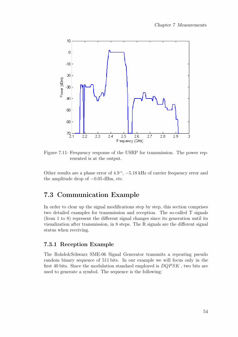
Chapter 7 Measurements
Figure 7.11: Frequency response of the USRP for transmission. The power rep-resented is at the output.
Other results are a phase error of 4.9 o, −5.18 kHz of carrier frequency error andthe amplitude drop of −0.05 dBm, etc.
7.3 Communication Example
In order to clear up the signal modifications step by step, this section comprisestwo detailed examples for transmission and reception. The so-called T signals(from 1 to 8) represent the different signal changes since its generation until itsvisualization after transmission, in 8 steps. The R signals are the different signalstatus when receiving.
7.3.1 Reception Example
The Rohde&Schwarz SME-06 Signal Generator transmits a repeating pseudorandom binary sequence of 511 bits. In our example we will focus only in thefirst 40 bits. Since the modulation standard employed is DQPSK , two bits areused to generate a symbol. The sequence is the following:
54

Chapter 7 Measurements
Figure 7.12: Filter frequency response [31].
R1
Generated sequence: 11 11 11 11 10 00 00 11 11 01 11 11 00 01 01 11 0011 00 10
Considering the generator is using Gray code, and that the procedure to pro-duce the differential sequence is adding each pair of bits at the input to a ac-cumulative 4-modulus cyclical sum, the generated sequence comes as shown insteps R2, R3 and R4:
R2
In decimal (Gray coding): 2 2 2 2 3 0 0 2 2 1 2 2 0 1 1 2 0 2 0 3
R3
Accumulative sum: 2 4 6 8 11 11 11 13 15 16 18 20 20 21 22 24 24 2626 29
55
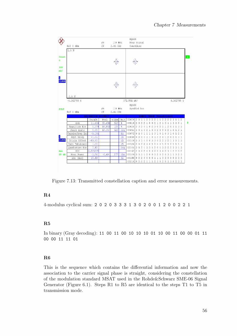
Chapter 7 Measurements
Figure 7.13: Transmitted constellation caption and error measurements.
R4
4-modulus cyclical sum: 2 0 2 0 3 3 3 1 3 0 2 0 0 1 2 0 0 2 2 1
R5
In binary (Gray decoding): 11 00 11 00 10 10 10 01 10 00 11 00 00 01 1100 00 11 11 01
R6
This is the sequence which contains the differential information and now theassociation to the carrier signal phase is straight, considering the constellationof the modulation standard MSAT used in the Rohde&Schwarz SME-06 SignalGenerator (Figure 6.1). Steps R1 to R5 are identical to the steps T1 to T5 intransmission mode.
56

Chapter 7 Measurements
Phase sequence: π 0 π 0 π2
π2
π2
−π2
π2
0 π 0 0 −π2
π 0 0 π π −π2
R7
This phase sequence in the carrier signal passes through the USRP and reachesthe demodulation block of the GRC. This block first produces an output sequenceresulting of calculating the difference between each phase value and the previousone, as follows:
Differential phase sequence: π π π π π2
0 0 π π −π2
π π 0 −π2
−π2
π 0 π0 π
2
R8
Decoding this sequence with the constellation diagram used in GNU Radio Com-panion (Figure 6.2) and using Gray coding results in:
Decoded binary sequence: 11 11 11 11 01 00 00 11 11 10 11 11 00 1010 11 00 11 00 01
Comparing transmitted and received sequence, it is easily proved the onlychange due to the unmatching constellations is solved by interchanging 0x01 and0x10, respectively.
All the steps can be seen in the next summary table (Table 7.2).
Table 7.2: Summary table for received signal treatment steps.
R1 11 11 11 11 10 00 00 11 11 01 11 11 00 01 01 ...R2 2 2 2 2 3 0 0 2 2 1 2 2 0 1 1 ...R3 2 4 6 8 11 11 11 13 15 16 18 20 20 21 22 ...R4 2 0 2 0 3 3 3 1 3 0 2 0 0 1 2 ...R5 11 00 11 00 10 10 10 01 10 00 11 00 00 01 11 ...R6 π 0 π 0 π
2π2
π2
−π2
π2
0 π 0 0 −π2
π ...R7 π π π π π
20 0 π π −π
2π π 0 −π
2−π2
...R8 11 11 11 11 01 00 00 11 11 10 11 11 00 10 10 ...
57
Chapter 7 Measurements
7.3.2 Transmission Example
T1
When transmitting a signal with GRC, the inserted decimal sequence in thevector source should be 255, 131, 223, 23 and 50, in order to get the next binaryoutputted sequence:
Generated sequence: 11 11 11 11 10 00 00 11 11 01 11 11 00 01 01 1100 11 00 10
T2
Considering the modulator at the GRC uses Gray coding, and that the procedureto code the sequence is adding each pair of bits at the input to a accumulative4-modulus cyclical sum, the produced sequence is obtain in steps T2, T3 and T4:
In decimal (Gray coding): 2 2 2 2 3 0 0 2 2 1 2 2 0 1 1 2 0 2 0 3
T3
Accumulative sum: 2 4 6 8 11 11 11 13 15 16 18 20 20 21 22 24 24 2626 29
T4
4-modulus cyclical sum: 2 0 2 0 3 3 3 1 3 0 2 0 0 1 2 0 0 2 2 1
T5
In binary (Gray decoding): 11 00 11 00 10 10 10 01 10 00 11 00 00 01 1100 00 11 11 01
T6
This sequence already contains the differential information, so just assigning di-rectly the phase value for each group of 2 bits, considering the constellationscheme employed by the GNU Radio Companion modulation block (Figure 6.3),the carrier phase sequence is:
Phase sequence: 5π4
π4
5π4
π4
7π4
7π4
7π4
3π4
7π4
π4
5π4
π4
π4
3π4
5π4
π4
π4
5π4
5π4
3π4
58

Chapter 7 Measurements
T7
This phase sequence in the carrier signal passes through the USRP and reachesthe Rohde&Schwarz FSQ-70 vector signal analyzer, where an output sequenceresulting of calculating the difference between each phase value and the previousone is obtained:
Differential phase sequence: π π π −π2
0 0 π π π2
π π 0 π2
π2
π 0 π 0 −π2
T8
Decoding this sequence with the constellation diagram used in the Rohde&SchwarzFSQ-70 vector signal analyzer (Figure 6.4):
Decoded binary sequence: 10 10 10 11 01 01 10 10 00 10 10 01 00 0010 01 10 01 11
Since the coding used to display the received symbols at the VSA is Non-Gray,the visible sequence is (Figure 7.14):2 2 2 3 1 1 2 2 0 2 2 1 0 0 2 1 2 1 3
Figure 7.14: Real transmitted sequence.
All the steps can be seen in the next summary table (Table 7.3).
59

Chapter 7 Measurements
Table 7.3: Summary table for transmitted signal treatment steps.
T1 11 11 11 11 10 00 00 11 11 01 11 11 00 01 01 ...T2 2 2 2 2 3 0 0 2 2 1 2 2 0 1 1 ...T3 2 4 6 8 11 11 11 13 15 16 18 20 20 21 22 ...T4 2 0 2 0 3 3 3 1 3 0 2 0 0 1 2 ...T5 11 00 11 00 10 10 10 01 10 00 11 00 00 01 11 ...T6 5π
4π4
5π4
π4
−π4
−π4
−π4
3π4
−π4
π4
5π4
π4
π4
3π4
5π4
...T7 π π π −π
20 0 π π π
2π π 0 π
2π2
...T8 10 10 10 11 01 01 10 10 00 10 10 01 00 00 ...
60

Chapter 8
Conclusions
In this thesis, I investigated the possible use of the software defined radio USRP1by Ettus as the main hardware component for an RF front-end for the satelliteground station at the Institute of Telecommunications at the Vienna University ofTechnology. After summarizing the parameters required of the satellite missionsconsidered and the ground station layout envisioned in Chapter 2 and Chapter 3,I analyzed the USRP hardware in Chapter 4 and the corresponding GNU RadioCompanion software in Chapter 5. For the transmission and reception measure-ments on the system, I selected a specific QPSK signal which I have described inChapter 6. The measurements are presented in Chapter 7.
I fully characterized the system for the transmission path from the digital sideto the RF output and for the reception path from RF input to the digital out-put in Chapter 7. Before the measurements I investigated the expected limitsin Chapter 4. The measurements include frequency response, gain, EVM, com-pression point, IIP3, dynamic range and BER. Since lots of the measurementscharacterize the system on a specific QPSK signal, I investigated the modula-tion and demodulation steps and give great details in Chapter 5, Chapter 6 andChapter 7.3.
For the final purpose of this ongoing project, which is the satellite communi-cation with the MOST, COROT and BRITE missions, an adaptation procedurehas to be carried out. In terms of frequency, as a first step, in order to enablethe full bandwidth when transmitting, the filter for ISM applications must be re-moved. Once both transmission and reception bands are fully available from 2.3to 2.9 GHz, the next task is to shift the frequency band covered to the satellites’working spectrum. Considering a fixed IF in the range from 100 MHz to approx-imately 500 MHz, the synthesizer used, the ADF4360-0, should be replaced foran ADF4360-2 in order to cover the band of interest from 2.00 GHz to 2.45 GHz.Further, amplifiers are necessary to adapt the signal power range of the USRPto the power levels of the satellites. When necessary, also modifications to theGRC blocks are possible, to provide different modulation schemes. After thesemodifications a deployment of the USRP in the ground station is possible.
Another prospective future application for the USRP is the use of the “RFX2400”daughterboard in a standalone configuration as the analog RF front-end to ex-isting modems. Here an adapter is necessary. This adapter has to provide both
61

Chapter 8 Conclusions
input and output interfaces for digital and analog signals, replacing the digitaland analog connections between daughterboard and motherboard. A microcon-troller is then necessary to set up daughterboard and the power has to be pro-vided by a separate power supply. This adapter would further enable an exclusivemeasurement of the daughterboard’s performance without the motherboard andGRC.
62

Acknowledgments
I would like to thank my supervisors Michael Fischer and Arpad L. Scholtzfor their patience and perseverance, and for their helpful guidance and supportthroughout this enriching diploma thesis. I am really glad of having come toVienna and having decided to take this thesis with them, which meant alreadyan asset for my prospective plans. This work has also been financially supportedby the Hochschuljubiläumsstiftung der Stadt Wien.
Thanks also to my labmates: To Javier Rodas for the knowledge transfer whenI really needed it, which helped me so much. And to my dear Amalia Lorca,my daily mate at laboratory, lunch, “semmel” and dinner time from Monday toSunday – because it was a pleasure being two desks away from her, eating so manylasagnas together and sharing either technical knowledge or personal experiences,and because we always found out the way to burst out laughing without apparentreason. She always helped me to have a more easygoing working period.
To all the friends I met during my Erasmus time in Vienna, especially men-tioning Ferrán Corzo, Rubén García, Elena López, María Gomeza, María Molina,Juan Guerra and Marta Montes. Thanks to them for believing in me and for thoseuncountable moments they were there for me with some cherish words, stupidjokes and never-ending smiles in their faces, which made me realize so many timeshow easy it is having a challenging project ahead when you have such friends byyour side. Particularly, to Xavier Escayola, nobody has encouraged me more thanhim, with his perfectly idealized and sometimes comically exaggerated image ofmyself. He gave me the confidence I needed, from the first to the last day of mywork, though at the end he was already gone.
I would like also to mention Guillermo Díez, a very important person for me,who, in spite of everything, was always willing to support me and help me fromthe beginning of my studies till the very end.
Y sobre todo lo demás, a las personas más importantes de mi vida, las quehan contribuido a todo esto desde que llegué a este mundo hasta ahora, 23 añosdespués. Porque de vosotros aprendí a ser la persona que soy, me despertasteistodas las inquietudes que he tenido y tengo, y me habéis apoyado en cada unade las decisiones que he tomado. Porque siempre lo habéis hecho todo por y paramí, me lo habéis dado todo, lo tuvierais o no y habéis creído en que si alguien escapaz de hacer algo, esa persona soy yo. Gracias Papá y Mamá. Y desde luegogracias a ti, Rober, porque desde pequeñín me hiciste sentir grande con tu vivamirada de admiración. Y a mi Yaya, quien en su cabeza, ya me ve como a unaastronauta.
63

Bibliography
[1] G. Maral, M. Bousquet, Satellite Communications Systems. Systems, Tech-niques and Technology, Leipzig, Verlag B.G. Teubner, 1992.
[2] David Calcutt, Laurie Tetley, Satellite Communications. Principles & Ap-plications, London, Melbourne, Auckland, Edward Arnold 1994.
[3] Alberto Martín Recuenco, SSETI Groundstation, Diploma Thesis, ViennaUniversity of Technology, 2008
[4] Werner Keim, Scientific Satellite Ground Station at 2 GHz in Urban Envi-ronment, Dissertation, Vienna University of Technology, 2004
[5] Ainhona Solana Estéban, Front-End Design for a Multi-Mission, Multi-Standard Satellite Ground Station, Diploma Thesis, Vienna University ofTechnology, 2010
[6] European Space Agency, ESA COROT, URL:http://www.esa.int/SPECIALS/COROT/, Last access in June 2011.
[7] Centre Nationale D’Études Spatiales, CNES COROT, URL:http://smsc.cnes.fr/COROT/index.htm, Last access in June 2011.
[8] Koudelka O., Egger G., Josseck B., Scholtz A., Deschamp N., CordellGrant C., Foisy D., Zee R., Weiss W., Keim W., Kuschnig R., TUGSAT-1/BRITEAustria – The First Austrian Nanosatellite, Acta Astronautica,Volume 64, Issues 11-12, June-July 2009, Pages 1144-1149.
[9] W.W. Weiss, J.M. Matthews, A.F.J. Moffat, MOST and BRITE Constel-lation, University of Vienna (Austria) & Austrian COROT, MOST andBRITE Constellation Consortia, University British Columbia & MOST Mis-sion Scientist, Universite de Montreal & Canadian BRITE-ConstellationConsortium.
[10] Ettus Research, Universal Software Radio Peripheral. The Foundation forComplete Software Radio Systems, Data Sheet, Mountain View, CA 94043
[11] Firas Abbas Hamza, The USRP under 1.5X Magnifying Lens!, Rev. 1.0,Last update: 12-June-2008.
[12] Altera, Altera Cyclone FPGA Family Overview, URL:http://www.altera.com/products/devices/cyclone/overview/
cyc-overview.html, 2010[13] Javier Rodas, José A. García-Naya, Carlos J. Escudero, Luis Castedo, GNU
RADIO. A New Paradigm for Software Defined Radio, University of ACoruña, A Coruña, Spain, 2010.
[14] Robert D. Strum, Donald E. Kirk, Discrete Systems and Digital Signal Pro-cessing, Addison Wesley, Massachusets, 1988
64

Bibliography
[15] Analog Devices, Mixed-Signal Front-End Processor for Broadband Commu-nications AD9860/AD9862*, URL:http://www.analog.com/static/imported-files/data_sheets/
AD9860_9862.pdf, Data Sheet, 2010[16] Mercury, Voltage Controlled Temperature Compensated Crystal Oscillators
VCTCXO, VM57T Series, CMOS Output, URL:http://www.mecxtal.com/pdf/vctcxo_vm57t.pdf, Data Sheet, 2008
[17] Ettus Research, USRP1 Schematics, Schematics, Mountain View, CA, 2005[18] Analog Devices, 800 MHz Clock Distribution IC, Dividers, Delay Adjust,
Three Outputs AD9513, URL:http://www.analog.com/static/imported-files/data_sheets/AD9513.pdf,Data Sheet, 2005
[19] Ettus Research, Flex2400 Schematics, Schematics, Mountain View, CA, 2006[20] Uwe Meyer-Baese, Digital Signal Processing with Field Programmable Gate
Arrays, Springer-Verlag, Florida, USA, 2007[21] Ettus Research, TX and RX Daughterboards. For the USRP Software Radio
System, Data Sheet, Mountain View, CA 94043[22] Avago Technologies, MGA-82563 0.1-6 GHz, 3 V, 17 dBm Amplifier, URL:
http://www1.futureelectronics.com/doc/AVAGO%20TECHNOLOGIES/
MGA-82563-BLKG.pdf, Data Sheet, 2006[23] Analog Devices, 0.8 GHz to 2.7 GHz Direct Conversion Quadrature Demod-
ulator AD8347, URL:http://www.analog.com/static/imported-files/data_sheets/AD8347.pdf,Data Sheet, 2005
[24] Analog Devices, Integrated Synthesizer and VCO ADF4360-0, URL:http://www.analog.com/static/imported-files/data_sheets/ADF4360-0.pdf,Data Sheet, 2004
[25] David D. Coleman, David A. Westcott, CWNA Certified Wireless NetworkAdministrator Official Study Guide, Sybex, Indiana, 2009
[26] Analog Devices, 700 MHz to 2700 MHz Quadrature Modulator AD8349,URL: http://www.analog.com/static/imported-files/data_sheets/AD8349.pdf, Data Sheet, 2004
[27] Analog Devices, Integrated Synthesizer and VCO ADF4360-2, URL:http://www.analog.com/static/imported-files/data_sheets/ADF4360-2.pdf,Data Sheet, 2006
[28] Glenn Zelniker, Fred J. Taylor, Advanced Digital Signal Processing. Theoryand Applications., Marcel Dekker, Inc., New York, Basel, Hong Kong, 1993
[29] Leon W. Couch, Digital and Analog Communication Systems, MaxwellMacmillan, International, 1990
[30] Ku Hyunchul, J.S. Kenney, Estimation of error vector magnitude using two-tone intermodulation distortion measurements, Microwave Symposium Di-gest, 2001 IEEE MTT-S International, Phoenix, AZ , USA, 2001
65

Bibliography
[31] Sawtek, 2441.8 MHz SAW Filte, URL:https://code.google.com/p/microembedded/downloads/detail?name=SAWTEK855916.pdf, Data Sheet
[32] Rohde & Schwarz, SME Signal Generator, URL:http://www2.rohde-schwarz.com/file_5530/sme_14e.pdf, Operating Man-ual, 1998
[33] Rohde & Schwarz, FSQ-K70/FSMR/FSU-B73 Application Firmware VSAExtension, URL:http://www2.rohde-schwarz.com/file_2898/FSQ-K70_SWManual_en.pdf, Soft-ware Manual, 2008
[34] Hittite, HMC174MS8 / 174MS8E GaAs MMIC T/R SWITCH DC - 3 GHz,URL:http://www.hittite.com/content/documents/data_sheet/hmc174ms8.pdf,Data Sheet
[35] Michael Fischer, 2, 6 GHz radio frequency front end for rapid prototyping,Diploma Thesis, Vienna University of Technology, 2006
[36] K. V. K. K. Prasad, Principles of digital communication systems and com-puter networks, Charles River Media, Massachusetts, 2004
66

List of Abbreviations
ADC Analog-to-Digital ConverterAPCO25 Association of Public Safety Communication Officials - Project
25BER Bit Error RateBPSK Binary Phase Shift KeyingBRITE BRIght Target ExplorerBW BandWidthCIC Cascaded Integrator-CombCOROT COnvection ROtation and planetary TransitsCP Compression PointDAC Digital-to-Analog ConverterDDC Digital Down ConverterDPSK Differential Phase Shift KeyingDQPSK Differential Quadrature Phase Shift KeyingDUC Digital Up ConverterEIRP Equivalent Isotropically Radiated PowerEVM Error Vector MagnitudeFFT Fast Fourier TransformFIR Finite Impulse ResponseFPGA Field Programmable Gate ArrayFSK Frequency Shift KeyingGEO Geostationary Earth OrbitGFSK Gaussian Frequency Shift KeyingGRC GNU Radio CompanionGUI Graphical User InterfaceIF Intermediate FrequencyIIP3 Third order Input Intercept PointINMARSAT INternational MARitime SATelliteISM Industrial, Scientific, MedicalISI Inter-Symbol InterferenceLEO Low Earth OrbitLHCP Left Handed Circular PolarizationLNA Low Noise AmplifierLP Linear PolarizationLPF Low-Pass FilterLSB Least Significant BitMEO Medium Earth Orbit
67

Bibliography
MIMO Multiple Input Multiple OutputMMIC Monolithic Microwave Integrated CircuitsMOST Microvariability and Oscillations of STarsMSAT Mobile SATelliteMSB Most Significant BitNADC North American Digital CellularNCO Numerical-Controlled OscillatorOQPSK Offset Quadrature Phase Shift KeyingPDC Personal Digital CellularPLL Phase-Locked LoopPSK Phase Shift KeyingQPSK Quadrature Phase Shift KeyingRF Radio FrequencyRHCP Right Handed Circular PolarizationRRC Root Raised CosineSMA Sub-Miniature version ASNR Signal to Noise RatioTCP Transmission Control ProtocolTDMA Time Division Multiple AccessTETRA TErrestrial Trunked RAdioTFTS Time and Frequency Transfer StandardTNC Terminal Node ControllerTTL Transistor-Transistor LogicUDP User Datagram ProtocolUHF Ultra High FrequencyUSB Universal Serial BusUSRP Universal Software Radio PeripheralVCO Voltage Controlled OscillatorVCTCXO Voltage Controlled Temperature Compensated Crystal
OscillatorVGS Vienna Ground StationVHF Very High FrequencyVSA Vector Signal AnalyzerWLAN Wireless Local Area NetworkXML eXtensible Markup Language
68

List of Figures
1.1 Satellite communications basic scenario . . . . . . . . . . . . . . . 2
3.1 Ground station diagram . . . . . . . . . . . . . . . . . . . . . . . 123.2 Universal Software Radio Peripheral . . . . . . . . . . . . . . . . . 133.3 RFX2400 Daughterboard . . . . . . . . . . . . . . . . . . . . . . . 133.4 USRP1 Motherboard . . . . . . . . . . . . . . . . . . . . . . . . . 14
4.1 USRP block diagram. . . . . . . . . . . . . . . . . . . . . . . . . . 164.2 FPGA digital down converter . . . . . . . . . . . . . . . . . . . . 194.3 FPGA digital up converter . . . . . . . . . . . . . . . . . . . . . . 20
5.1 GRC front-end receiver scenario . . . . . . . . . . . . . . . . . . . 245.2 Data flow graph in the demodulation block . . . . . . . . . . . . . 265.3 Parameter settings for the demodulator block . . . . . . . . . . . 265.4 Constellation output after the automatic gain control block . . . . 275.5 Constellation output after the root raised cosine filter . . . . . . . 285.6 Constellation output after synchronization . . . . . . . . . . . . . 305.7 Calculated distances from an undecoded received symbol to each
of the reference points . . . . . . . . . . . . . . . . . . . . . . . . 315.8 Constellation output after decoding . . . . . . . . . . . . . . . . . 325.9 GRC front-end transmitter scenario . . . . . . . . . . . . . . . . . 335.10 Data flow graph in the modulation block . . . . . . . . . . . . . . 355.11 Parameter settings for the modulator block . . . . . . . . . . . . . 355.12 Constellation output after coding . . . . . . . . . . . . . . . . . . 37
6.1 MSAT modulation constellation scheme . . . . . . . . . . . . . . . 406.2 GRC demodulation constellation scheme . . . . . . . . . . . . . . 406.3 GRC modulation constellation scheme . . . . . . . . . . . . . . . 426.4 INMARSAT demodulation constellation scheme . . . . . . . . . . 42
7.1 Frequency response of the USRP for reception . . . . . . . . . . . 447.2 Attenuation response for the dynamic range analysis . . . . . . . 467.3 Gain response and compression point . . . . . . . . . . . . . . . . 477.4 Intermodulation products of two-tone measurement . . . . . . . . 487.5 Third order intercept point . . . . . . . . . . . . . . . . . . . . . . 497.6 Bit error rate depending on the input power . . . . . . . . . . . . 507.7 Logarithmic graph of the bit error rate . . . . . . . . . . . . . . . 517.8 Bit error distribution . . . . . . . . . . . . . . . . . . . . . . . . . 52
69

List of Figures
7.9 Bit error rate depending on the frequency offset . . . . . . . . . . 537.10 Lock and capture frequency ranges . . . . . . . . . . . . . . . . . 537.11 Frequency response of the USRP for transmission . . . . . . . . . 547.12 Filter frequency response . . . . . . . . . . . . . . . . . . . . . . . 557.13 Transmitted constellation caption and error measurements . . . . 567.14 Real transmitted sequence . . . . . . . . . . . . . . . . . . . . . . 59
70

List of Tables
2.1 Uplink and downlink frequency values . . . . . . . . . . . . . . . . 52.2 Uplink and downlink power (EIRP) levels . . . . . . . . . . . . . 62.3 Uplink and downlink power densities . . . . . . . . . . . . . . . . 62.4 Uplink and downlink data rates . . . . . . . . . . . . . . . . . . . 62.5 Uplink and downlink modulation standards . . . . . . . . . . . . . 72.6 Other parameters of the satellite missions . . . . . . . . . . . . . . 8
5.1 Mapping and unpacking summary . . . . . . . . . . . . . . . . . . 32
7.1 Maximum power, gain, IIP3, CP and noise figure of the mainelements is the receiver chain . . . . . . . . . . . . . . . . . . . . 45
7.2 Summary table for received signal treatment steps . . . . . . . . . 577.3 Summary table for transmitted signal treatment steps . . . . . . . 60
71


![A New Stereo Benchmarking Dataset for Satellite Images · ests) in San Fernando, Argentina, as defined in the IARPA’s MVS Challenge dataset [7]. That challenge dataset, span-ning](https://static.fdocuments.net/doc/165x107/60a2bbf95511a421c422480a/a-new-stereo-benchmarking-dataset-for-satellite-images-ests-in-san-fernando-argentina.jpg)