Soft-Switching, Interleaved Inverter for High Density Applications · 2020-01-22 ·...
55
Soft-Switching, Interleaved Inverter for High Density Applications Rachael G. Born Thesis submitted to the faculty of the Virginia Polytechnic Institute and State University in partial fulfillment of the requirements for the degree of Master of Science In Electrical Engineering Jih-Sheng Lai, Chair Qiang Li Daniel Sable September 14 th , 2016 Blacksburg, Virginia Keywords: soft-switching, wide bandgap, DC-AC Copyright 2016 Rachael G. Born
Transcript of Soft-Switching, Interleaved Inverter for High Density Applications · 2020-01-22 ·...
Soft-Switching, Interleaved Inverter for High
Density Applications
Rachael G. Born
Thesis submitted to the faculty of the
Virginia Polytechnic Institute and State University
in partial fulfillment of the requirements for the degree of
Master of Science
In
Electrical Engineering
Jih-Sheng Lai, Chair
Qiang Li
Daniel Sable
September 14th
, 2016
Blacksburg, Virginia
Keywords: soft-switching, wide bandgap, DC-AC
Copyright 2016 Rachael G. Born

Soft-Switching, Interleaved Inverter for High Density
Applications
Rachael G. Born
Abstract
Power density has become increasingly important for applications where weight and
space are limited. Power density is a unique challenge requiring the latest transistor technology
to push switching frequency to shrink passive filter size. Furthermore, while high efficiency is an
important thermal handling strategy, it must be weighed against increases in component size.
Google’s Little Box Challenge shone light on these challenges in pushing the power density of a
2kW inverter. The rise in electric vehicle infrastructure and demand represents a unique
application for power electronics: pushing the power handling capability and functionality of bi-
directional, on-board electric vehicle chargers for faster charging while simultaneously shrinking
them in size.
New wide-bandgap (WBG) devices, combined with soft-switching, now allow inverters
to shrink in size by pushing to higher switching frequencies while maintaining efficiency. Classic
H-Bridge topologies have limited switching frequency due to hard switching. Soft switching
allows inverters to operate at higher frequency while minimizing switching loss. Concurrently,
interleaving can reduce current handling stress and conduction loss better than simply paralleling
two transistors.
A novel interleaved auxiliary resonant snubber for high-frequency soft-switching is
introduced. The design of an auxiliary resonant snubber is discussed; this allows the main GaN
MOSFETs to achieve zero voltage switching (ZVS). The auxiliary switches and SiC diodes
achieve zero current switching (ZCS). This soft-switching strategy can be applied to any
modulation scheme. Here, it is applied to an asymmetrical unipolar H-bridge with two high
frequency legs interleaved. While soft-switching minimizes switching loss, conduction loss is
simultaneously reduced for high-power applications by interleaving two high frequency legs.
This topology is chosen for its conduction loss reduction and bi-directional capability.

Soft-Switching, Interleaved Inverter for High Density
Applications
Rachael G. Born
General Audience Abstract
Electric vehicles have become a unique application for power electronics where battery
chargers must both handle higher power and shrink in size and weight. The latest transistor
technology allows the designer to push switching frequency, shrinking the size of components
and increasing the power density. In 2014, Google’s Little Box Challenge shone light on the
design trade-offs of high power density design with new transistor technology for a 2kW
inverter.
New semi-conductor materials now allow transistors to switch at higher frequency with
less loss. To take advantage of these features, a new switching method is developed. The main
power transistors are brought to zero voltage before turn-on with auxiliary switches and resonant
current. Interleaving is added for better efficiency and power handling. With further control, this
method could prove attractive for new, high-density power electronic designs. Applications for
this include bi-directional chargers for electric vehicles in the 6kW range.

iv
Acknowledgements
First, I would like to express my deep appreciation to my advisor, Dr. Jih-Sheng Lai. Dr. Lai
has been instrumental in opening up new avenues for me to learn and develop myself as an
electrical engineer in the field of power electronics. With his guidance, I have learned far more
than any classroom could teach, preparing me for a career beyond school. I would also like to
thank Dr. Sable and Dr. Li for being some of the best professors I have had at Virginia Tech and
for serving on my committee and providing helpful suggestions and support.
To everyone at Future Energy Electronics Center (FEEC) who mentored and befriended me,
thank you for your kindness and passion. The insight and knowledge I have gained from
discussions with all of you have been absolutely invaluable. For their help and support I would
like to thank Lanhua Zhang, Xiaonan Zhao, Jason Dominic, Thomas LaBella, Chih-Shen Yeh,
Baifeng Chen, Ben York, Nathan Kees, Eric Faraci, Seungryul Moon, Hidekazu Miwa, and Gary
Kerr. I would also like to thank Mr. Curt Maxey for introducing me to the world of electrical
engineering during my internship at Oak Ridge National Lab.
Finally, I would like to thank my Dad for his unerring support and encouragement
throughout all of my crazy plans and all of the hurdles we have faced together.

v
Table of Contents
1 Introduction ........................................................................................................................... 1
1.1 Level 2 EV charging ........................................................................................................ 1
1.2 Achieving High Power Density and Google’s Little Box Challenge............................... 3
1.3 Achieving Zero Voltage Switching ................................................................................ 11
1.4 Goal and Scope of Thesis ............................................................................................... 17
2 Inverter Operation .............................................................................................................. 18
2.1 ZVS Operation ............................................................................................................... 18
3 Design Tradeoffs and Prototype Hardware Selection ...................................................... 24
3.1 Dead Time and the Resonant Circuit ............................................................................. 24
3.2 Resonant Component Design Tradeoffs ........................................................................ 26
3.3 Switching frequency ....................................................................................................... 27
3.4 DC Bus Voltage ............................................................................................................. 28
3.5 Auxiliary Active Component Selection ......................................................................... 29
3.6 Main Switch Selection for High Frequency Legs .......................................................... 30
3.7 Challenges in Driving GaN ............................................................................................ 31
3.8 Main Switch Selection for Low Frequency Leg ............................................................ 34
3.9 Output Filter .................................................................................................................... 34
4 Design Summary .................................................................................................................. 36
4.1 Hardware Test Setup ....................................................................................................... 36
4.2 Soft-switching ................................................................................................................. 38
4.3 Power Density ................................................................................................................ 38
4.4 Zero Crossing Issue ........................................................................................................ 40
5 Conclusion ............................................................................................................................ 45
6 Citations ................................................................................................................................ 46

vi
List of Figures
Figure 1. On-board and off-board charging infrastructure. CC/CV means that batteries are
charged with either constant current or constant voltage .................................................... 3
Figure 2. Summary of FEEC Little Box Challenge Results ........................................................... 4
Figure 3. Hard switching interleaved inverter topology ................................................................. 4
Figure 4. Operation of full bridge inverter with asymmetrical unipolar modulation ..................... 6
Figure 5. Operation of unipolar, full-bridge inverter with synchronous rectification .................... 8
Figure 6. Hard switching interleaved inverter with unipolar modulation ..................................... 10
Figure 7. Auxiliary Resonant Snubber requires bipolar switching ............................................... 12
Figure 8. Auxiliary Resonant Snubber with single coupled inductor ........................................... 13
Figure 9. Auxiliary resonant snubber with two coupled inductors ............................................... 14
Figure 10. Google Little Box Challenge Team auxiliary soft-switching design .......................... 15
Figure 11. In simulation, a current loop developed between the two auxiliary legs of this ZVS
design ................................................................................................................................ 16
Figure 12. Proposed soft-switching interleaved inverter topology ............................................... 18
Figure 13. Topological and timing circuit operation. ................................................................... 22
Figure 14. Output current direction and magnitude impact on natural ZVS ................................ 23
Figure 15. Equivalent circuit during resonant period ................................................................... 25
Figure 16. Resonant Current over high frequency leg switching period ...................................... 29
Figure 17. Equivalent electrical configuration of Silicon Labs gate driver signal input .............. 31
Figure 18. Layout for added reliability of gate drive circuit ......................................................... 31
Figure 19. Gating and Switch layout for Little Box Challenge PCB ............................................ 32
Figure 20. Modified bootstrap circuit for GaN transistor gate voltage supply ............................. 33
Figure 21. Altium PC Board layout .............................................................................................. 37
Figure 22. Assembled prototype for testing .................................................................................. 37
Figure 23. Auxiliary resonant circuit assists main switch to achieve ZVS .................................. 38
Figure 24. Autocad model of soft-switching interleaved inverter ................................................ 39
Figure 25. PCB size for hard switching topology (left) and soft switching topology (right) ....... 40
Figure 26. Synchronized turn-on and turn-off of gate signals at zero crossing points. ................ 41
Figure 27. Zero crossing waveforms as a result of synchronized turn-on/off. ............................. 42

vii
Figure 28. Modified gating waveforms at zero crossing. The yellow and red waveforms control
the low frequency legs and the green and blue waveforms control the main switches of a
single high frequency leg. ................................................................................................. 43
Figure 29. Spikes in current remain despite the simplified gating around the zero crossing ....... 43
Figure 30. Level of spiking on input and output current waveforms (bright and dark green,
respectively) relative to level of current. The blue waveform is drain-source voltage of a
low frequency switch and the red is the drain-source voltage of a high frequency switch.
........................................................................................................................................... 44

viii
List of Tables
Table 1. Electric Vehicle Charging Categories............................................................................... 1
Table 2. Prototype Specifications ................................................................................................. 24
Table 3. Core Material Options for Resonant Inductor ................................................................ 27
Table 4. Switching frequency design tradeoffs ............................................................................. 28
Table 5. Summary of prototype design ......................................................................................... 36

1
1 Introduction
Power density has become increasingly important in high-power applications such as electric
vehicles, more-electric aircraft, and solar power. When space and weight are limited, design
must focus on balancing both efficiency and component size.
As active components have continued to decrease in size while increasing in functionality,
passive components – i.e. inductors and capacitors - have remained mostly unchanged. Reducing
passive component size requires operating at higher frequencies. To push efficient inverters into
switching at hundreds of kilohertz, both wide-bandgap devices and soft-switching schemes must
be implemented. Wide-bandgap devices, such as GaN and SiC, offer faster turn-on and turn-off
times, less turn-off loss, and a decrease in parasitic capacitance – all while shrinking package
size [1].
First, an outline of several considerations in selecting a topology is presented; then, the
detailed workings and control of one solution is introduced: an interleaved inverter with auxiliary
resonant snubber.
1.1 Level 2 EV charging
Plug-in Hybrid Electric Vehicles (PHEV) and Electric Vehicles (EV) are on the cusp of
becoming significant elements of world-wide auto sales. In addition to Tesla’s 400,000 pre-
orders for their upcoming Model 3 [2], traditional auto makers are entering the market with
GM’s Chevy Bolt, Nissan’s extended range Leaf, and Ford’s expected Model E – all of which
plan to offer 200 mile range at around $35,000 [3].
EV and PHEV batteries can be charged at a variety of a speeds, depending on the power
level. These speeds are generally grouped into three categories and are described in Table 1.
Table 1. Electric Vehicle Charging Categories [4]
Supply Voltage Power Level Charging Speed
Level 1 Charger 120 V AC 1.2kW 2-5 miles / 1 hour of charging
Level 2 Charger 208-240 V AC 3.3kW-20kW 10-20 miles/ 1 hour of charging
DC Fast Charger DC up to 480V 20kW – 120kW 50-70 miles/ 20 min of charging

2
Level 1 charging is akin to plugging an electric vehicle into a normal 120V outlet at the car
owner’s home or work. While slow, this method requires no extra hardware and can successfully
charge a vehicle overnight. Level 2 charging can charge a vehicle in half the time as level 1
charging but requires plugging the car into a 240V outlet, though this is also commonly available
in households for high-power appliances like dryers and hot water heaters. The ability to plug an
electric vehicle directly into an outlet requires an on-board charger to convert the AC power of
the grid to the proper DC voltage and current for battery charging. While convenient, this
onboard charger consumes precious weight and space on the vehicle. Thus, level 2 charging is
limited by the level of power the on-board charger can handle: 3.3kW for most PHEV’s and
6.6kW-10kW for most EV’s [5]. Without external charging equipment, charging speed is limited
by the on-board charger’s power handling capability.
DC fast charging stations offer a wide range of faster charging times: from a couple of hours
to a couple of minutes. The high power levels for fast charging require significant investment in
a hardware off-board charger and may reduce the battery life if done regularly. These charging
stations are for commercial applications to allow drivers to quickly recharge during longer road
trips.
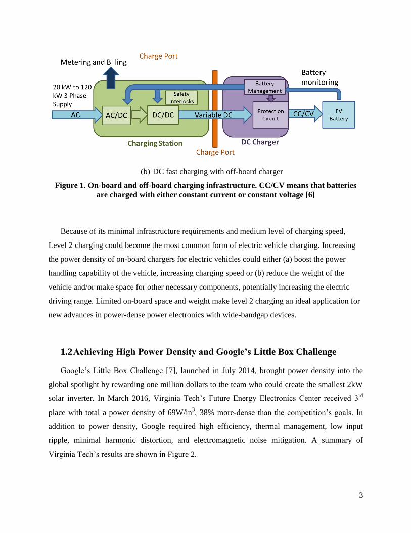
The different hardware requirements for on-board and off-board charging methods are
summarized in Figure 1. While the main purpose of EV chargers is delivering power from the
grid to the car batteries, bi-directional capabilities may be useful in the future for grid
stabilization and even back-up power.
(a) Level 1 and 2 charging with on-board charger
3
(b) DC fast charging with off-board charger
Figure 1. On-board and off-board charging infrastructure. CC/CV means that batteries
are charged with either constant current or constant voltage [6]
Because of its minimal infrastructure requirements and medium level of charging speed,
Level 2 charging could become the most common form of electric vehicle charging. Increasing
the power density of on-board chargers for electric vehicles could either (a) boost the power
handling capability of the vehicle, increasing charging speed or (b) reduce the weight of the
vehicle and/or make space for other necessary components, potentially increasing the electric
driving range. Limited on-board space and weight make level 2 charging an ideal application for
new advances in power-dense power electronics with wide-bandgap devices.
1.2 Achieving High Power Density and Google’s Little Box Challenge
Google’s Little Box Challenge [7], launched in July 2014, brought power density into the
global spotlight by rewarding one million dollars to the team who could create the smallest 2kW
solar inverter. In March 2016, Virginia Tech’s Future Energy Electronics Center received 3rd
place with total a power density of 69W/in3, 38% more-dense than the competition’s goals. In
addition to power density, Google required high efficiency, thermal management, low input
ripple, minimal harmonic distortion, and electromagnetic noise mitigation. A summary of
Virginia Tech’s results are shown in Figure 2.

4
Figure 2. Summary of FEEC Little Box Challenge Results
To achieve these objectives, two stages were used: a DC/DC stage to control the input ripple
and decrease bus voltage and a DC/AC stage to convert the input DC voltage to AC power
suitable for the grid. Furthermore, wide-bandgap (WBG) devices such as Gallium Nitride (GaN)
and Silicon Carbide (SiC) provided new opportunities to efficiently push power density.
Mechanically, CAD software ensured full utilization of space with components selected by both
electrical and form-fitting requirements. GaN switches for the DC/DC stage and DC/AC stage
were directly heat-sinked to the lid and case, respectively, allowing the copper case to double as
a heat sink and keeping hotter areas toward the surface for easier dissipation.
For the DC to AC stage, a high-efficiency interleaved inverter was developed to push power
density in a 2kW solar inverter for Google’s little box challenge [8] as seen in Figure 3. Here,
Q1-Q4 were switched at high frequency and the two legs interleaved. Q5 and Q6 were switched
at line frequency. By interleaving two high frequency legs, this topology reduces current stress
on the main power MOSFETs, minimizing conduction losses while shrinking output inductor
size requirements. Furthermore, GaN MOSFETs eliminated reverse recovery losses during hard
switching, allowing the inverter stage to reach over 99% efficiency with 60kHz switching.
Figure 3. Hard switching interleaved inverter topology [8]

5
The following sections will detail the origins, benefits, and operation of the interleaved inverter.
a) Full bridge inverter with asymmetrical unipolar modulation
The design introduced in Figure 3 is based on a full-bridge inverter topology with
asymmetrical unipolar modulation [9]. The operation of the full bridge topology is described in
Figure 4. Two 60Hz reference waveforms are compared with a triangle carrier at the desired high
switching frequency to produce the proper duty cycle. During the first half cycle, S1 switches at
a high frequency while S3 is continuously on. When S1 is on, current travels through the
MOSFET, charges the output filter inductor, and travels through S3. When S1 is off, the body
diode of the bottom high frequency device (S2) conducts and the inductor discharges in a current
loop. During the second half cycle, this operation is mirrored in the other two devices. S2
switches at a high frequency while S5 is continuously on. When S2 is on, current travels through
S5, charges the output filter inductor, and travels through S2. When S2 is off, the body diode of
the top high frequency device (S1) conducts and the inductor discharges through the current
loop.

6
(a) Positive half cycle operation
(b) Negative half cycle operation
Figure 4. Operation of full bridge inverter with asymmetrical unipolar modulation
Because of the unipolar modulation, the voltage between the mid-point of the two legs,
Vab, has three levels and requires a smaller output filter than bipolar modulation.

7
a) Synchronous rectification of H-bridge
The modulation in Figure 4 relies heavily on the MOSFET’s body diode, which can have
undesirable characteristics. In silicon devices, the forward drop of the body diode can be less
than a volt. With GaN devices, the body diode has the advantage of zero reverse recovery charge
but the disadvantage of a forward voltage drop of at least 2V – depending on the manufacturer
and current level, the voltage drop could be even higher than 6V. One common way to improve
the efficiency of this design is to introduce synchronous rectification. Here, instead of the body
diode conducting when the partner high frequency switch is off, the MOSFET is turned on and
conducts through the channel. This method can also help the inverter handle non-unity power
factor loads by allowing current to flow in either the positive or negative direction if the voltage
and current waveforms are out of phase. Handling non-unity power factor loads was one of the
requirements of Google’s Little Box Challenge and is necessary for connecting PV to the grid. It
also ensures that the inverter can operate bi-directionally (given the proper control feedback) as
either an inverter or rectifier. The resultant change in gate signals and operation can be seen in
Figure 5.

8
(a) Positive half cycle operation
(b) Negative half cycle operation
Figure 5 Operation of unipolar, full-bridge inverter with synchronous rectification
b) Operation of hard-switching, interleaved inverter
The final alteration to the basic H-bridge topology introduced in sections (a) and (b) to
achieve the design of Figure 3 is to add a second high frequency leg. For high current
G1
G1
G2
G2

9
applications, it is common to parallel two MOSFETs together to share the current load and cut
the conduction loss in half. While this technique reduces conduction loss in the MOSFETs
themselves, it does not impact the conduction loss or size of the output filter inductor.
Interleaving two high frequency legs effectively splits the full load current between two
legs, impacting not just the MOSFETs but also the output filter. Interleaving can theoretically cut
the overall MOSFET conduction loss in half and the overall filter inductor conduction loss in
half. The filter inductor wire can also be sized to handle a smaller current, allowing for the use of
two smaller inductors instead of one large one and potentially shrinking the overall volume of
the inductors. Furthermore, to interleave the two legs, the triangle carriers for the two high
frequency legs are placed 180 degrees apart. The ripple on the two output current waveforms is
also 180 degrees out of phase and cancels each other, further reducing output filter size
requirements.
Thus, when compared with just paralleling two devices, interleaving offers better
efficiency and a reduced output filter size with no additional components. Operation of the
inverter with two interleaved high frequency legs and synchronous rectification is summarized in
Figure 6.

10
(a) Interleaved inverter topology
(b) Modulation waveforms for interleaved inverter topology with unipolar modulation.
The three PWM signals control the top switch for the two high frequency legs (red for
S1 and dark red for S3) and the top switch of the low frequency leg (S5 in orange).
Figure 6. Hard switching interleaved inverter with unipolar modulation
Google’s Little Box Challenge (LBC) pushed the power density for a 2kW solar inverter,
which is about the power level required for a typical home PV installation of eight panels. Yet
the volume of solar panels themselves and decreasing solar power system costs make the power
density of the inverter itself less of a critical factor. Yet, lessons from the LBC can be applied to
an area where weight and volume are critical: on-board electric vehicle charging.
G1 G2
G3 G4
11
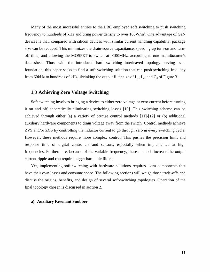
Many of the most successful entries to the LBC employed soft switching to push switching
frequency to hundreds of kHz and bring power density to over 100W/in3. One advantage of GaN
devices is that, compared with silicon devices with similar current handling capability, package
size can be reduced. This minimizes the drain-source capacitance, speeding up turn-on and turn-
off time, and allowing the MOSFET to switch at >100MHz, according to one manufacturer’s
data sheet. Thus, with the introduced hard switching interleaved topology serving as a
foundation, this paper seeks to find a soft-switching solution that can push switching frequeny
from 60kHz to hundreds of kHz, shrinking the output filter size of L1, L2, and Co of Figure 3 .
1.3 Achieving Zero Voltage Switching
Soft switching involves bringing a device to either zero voltage or zero current before turning
it on and off, theoretically eliminating switching losses [10]. This switching scheme can be
achieved through either (a) a variety of precise control methods [11]-[12] or (b) additional
auxiliary hardware components to drain voltage away from the switch. Control methods achieve
ZVS and/or ZCS by controlling the inductor current to go through zero in every switching cycle.
However, these methods require more complex control. This pushes the precision limit and
response time of digital controllers and sensors, especially when implemented at high
frequencies. Furthermore, because of the variable frequency, these methods increase the output
current ripple and can require bigger harmonic filters.
Yet, implementing soft-switching with hardware solutions requires extra components that
have their own losses and consume space. The following sections will weigh those trade-offs and
discuss the origins, benefits, and design of several soft-switching topologies. Operation of the
final topology chosen is discussed in section 2.
a) Auxiliary Resonant Snubber
12
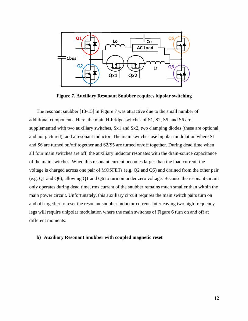
Figure 7. Auxiliary Resonant Snubber requires bipolar switching
The resonant snubber [13-15] in Figure 7 was attractive due to the small number of
additional components. Here, the main H-bridge switches of S1, S2, S5, and S6 are
supplemented with two auxiliary switches, Sx1 and Sx2, two clamping diodes (these are optional
and not pictured), and a resonant inductor. The main switches use bipolar modulation where S1
and S6 are turned on/off together and S2/S5 are turned on/off together. During dead time when
all four main switches are off, the auxiliary inductor resonates with the drain-source capacitance
of the main switches. When this resonant current becomes larger than the load current, the
voltage is charged across one pair of MOSFETs (e.g. Q2 and Q5) and drained from the other pair
(e.g. Q1 and Q6), allowing Q1 and Q6 to turn on under zero voltage. Because the resonant circuit
only operates during dead time, rms current of the snubber remains much smaller than within the
main power circuit. Unfortunately, this auxiliary circuit requires the main switch pairs turn on
and off together to reset the resonant snubber inductor current. Interleaving two high frequency
legs will require unipolar modulation where the main switches of Figure 6 turn on and off at
different moments.
b) Auxiliary Resonant Snubber with coupled magnetic reset
13
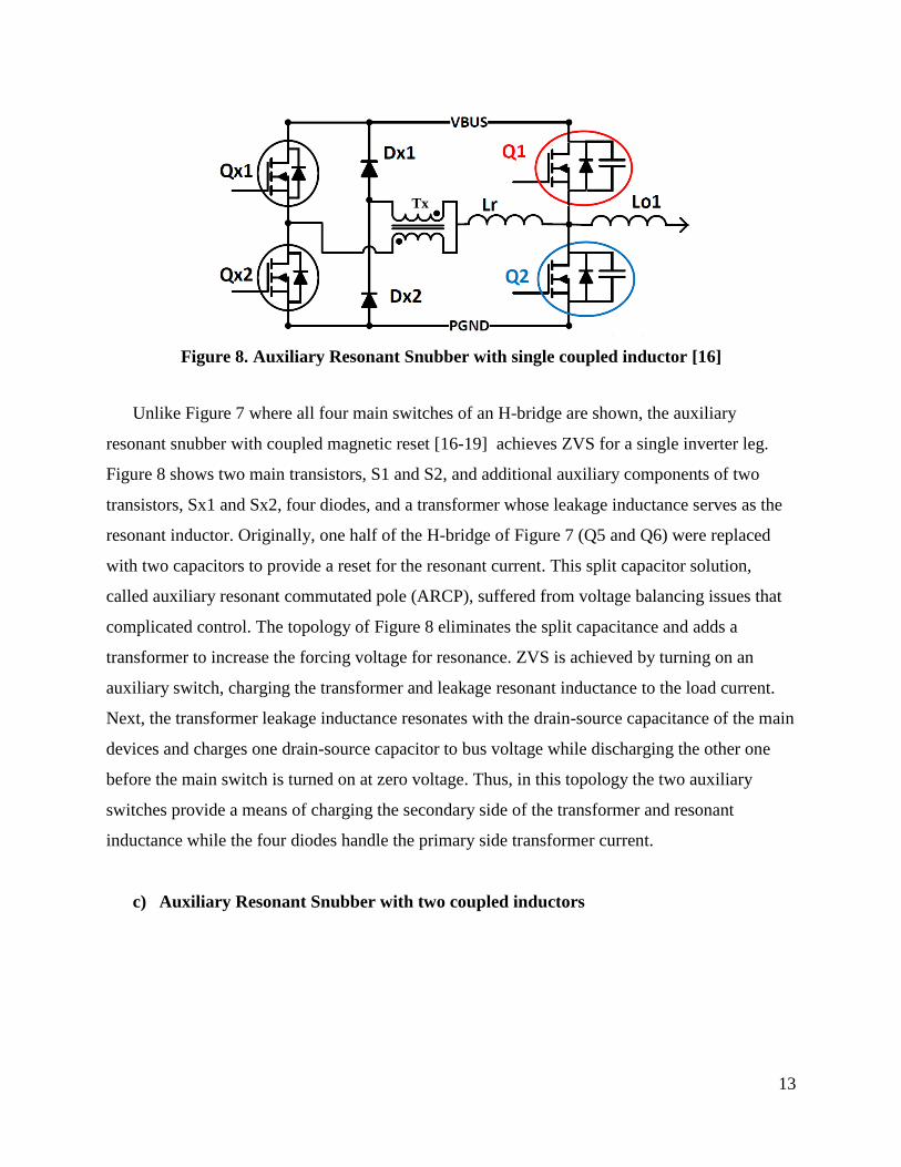
Figure 8. Auxiliary Resonant Snubber with single coupled inductor [16]
Unlike Figure 7 where all four main switches of an H-bridge are shown, the auxiliary
resonant snubber with coupled magnetic reset [16-19] achieves ZVS for a single inverter leg.
Figure 8 shows two main transistors, S1 and S2, and additional auxiliary components of two
transistors, Sx1 and Sx2, four diodes, and a transformer whose leakage inductance serves as the
resonant inductor. Originally, one half of the H-bridge of Figure 7 (Q5 and Q6) were replaced
with two capacitors to provide a reset for the resonant current. This split capacitor solution,
called auxiliary resonant commutated pole (ARCP), suffered from voltage balancing issues that
complicated control. The topology of Figure 8 eliminates the split capacitance and adds a
transformer to increase the forcing voltage for resonance. ZVS is achieved by turning on an
auxiliary switch, charging the transformer and leakage resonant inductance to the load current.
Next, the transformer leakage inductance resonates with the drain-source capacitance of the main
devices and charges one drain-source capacitor to bus voltage while discharging the other one
before the main switch is turned on at zero voltage. Thus, in this topology the two auxiliary
switches provide a means of charging the secondary side of the transformer and resonant
inductance while the four diodes handle the primary side transformer current.
c) Auxiliary Resonant Snubber with two coupled inductors
Tx

14
Figure 9 Auxiliary resonant snubber with two coupled inductors [20]
One problem with the auxiliary resonant snubber with one coupled inductor, resulting in the
proposal of the topology in Figure 9, is that if the magnetizing current is not fully reset the
transformer core may saturate. The auxiliary resonant snubber with two coupled magnetics [20,
21] solves this issue by implementing two coupled inductors for faster and more reliable
magnetizing current reset. As in the single transformer configuration, the two auxiliary switches
drive the resonance while four diodes conduct the primary side of the transformer. This
configuration has been demonstrated to be highly reliable and efficient, demonstrating in [20]
over 99% CEC efficiency for a 4kW PV application.
While pushing to higher frequencies reduces the output filter size, the size of the auxiliary
elements is related to dead time and will add to the overall size of the inverter regardless of
switching frequency. Thus, the additional size of auxiliary components must be weighed against
any size reduction achieved by reaching higher frequencies. Topology (c) is both efficient and
reliable at low frequencies. However, the resonant inductance of the auxiliary resonant snubber
with either single or double transformers is generated by the leakage inductance of the
transformer. To generate enough leakage inductance for resonance, magnetizing inductance must
be significantly larger. With higher switching frequencies, the two transformers do not change in
size and can become much larger than the output filter inductor.
d) Little Box Challenge AMR team

15
Figure 10. Google Little Box Challenge Team auxiliary soft-switching design
The AMR team of the little box challenge [22] came up with a dc-dc converter topology that
eliminates the large transformer that plagued the power density of the topologies introduced in
(b) and (c). Instead, smaller inductors are directly used for resonance. Although the passive
component size is decreased, the total number of auxiliary components remain unchanged: two
transistors, 4 diodes, and two inductors.
Another advantage of the topology in Figure 10 is that the resonant current should only be
present during dead time. This reduces conduction loss and eliminates the worry of magnetic
current reset timing. The auxiliary resonant snubber with coupled inductors in sections (b) and
(c) allowed resonant current to flow during both dead time and normal operation, forcing current
reset to occur quickly within the dead time.
Yet, in simulations of Figure 10 it was found that the resonant current never returned to zero
and continued to circulate beyond the dead time. This could increase the rms current and losses
in the auxiliary circuit. As shown in Figure 11, during dead time if the top auxiliary switch Qx1
is turned on, D4 blocks the full bus voltage and the inductor current of L2 begins to charge to the
load current. During resonance, when auxiliary current surpasses output current, some current
also begins to flow through L1 and D2, charging Qx2 from zero to the bus voltage at the same
time Q2 is being charged. Even after Q1 turns on under ZVS, the two auxiliary inductors are still
charged and continue to circulate current through a loop where the voltage across Qx1 and Qx2
is slightly larger than the voltage across Q2, according to the simulation results.

16
(a) Simulation waveform shows unwanted current continues to flow in auxiliary circuit
outside of dead time. The dark blue waveform of I(Lx2) begins conducting current
during the resonant period even though the current through I(Lx1) is the only
assistant current needed for ZVS. During normal operation after dead time, as the
output current (brown I Lo1) begins to ramp up, the current through I(Q1) remains
larger to supply both the output and unwanted current loop
(b) Circuit diagram of unwanted current loop
Figure 11. Current loop between the two auxiliary legs of this ZVS design allowed current
to flow through auxiliary circuit beyond dead time.

17
To prevent this, two inductors are reduced to one and D2 and D3 become linked. Now, when
Qx1 is turned on, D4 and Qx2 immediately block the bus voltage. Furthermore, during resonance
current can only flow through the inductor in one direction, preventing the unwanted current
loop from developing. Paring two auxiliary inductors down to one further reduces the size of this
ZVS method. The single auxiliary inductor does not conduct twice as much current, but rather is
used for ZVS for the entire 60Hz cycle rather than for half a cycle. A more detailed discussion of
circuit operation will be held in Section 2.
1.4 Goal and Scope of Thesis
The goal of this thesis is to push the power density of the inverter stage of a level two, on-
board electric vehicle charger.
While Figure 1 shows the flow of power of an on-board electric vehicle charger in one
direction (from the grid to the battery) research is increasingly looking toward bi-directional
electric vehicle chargers to provide power to the future smart grid in peak demand moments.
Here, for ease in comparison to the previously developed hard-switching inverter (described in
section 1.2), this topology is tested as an inverter. Because the topology can handle bi-directional
power flow, future control loop design will allow it to operate as a traditional rectifier. As a
rectifier, “asymmetrical unipolar” modulation (discussed in section 1.2 part a) is more commonly
referred to as a “totem pole PFC”.
The scope of this thesis is to prove the functionality of a novel soft-switching method by
designing, simulating, building, and testing an inverter prototype. This soft switching method can
be used on any half bridge leg, regardless of modulation method. The auxiliary resonant snubber
is combined with a new interleaved topology developed for the little box challenge and switching
frequency is pushed to hundreds of kilohertz.
The following sections will detail operation of the inverter, design tradeoffs and
considerations, and experimental results from prototype testing.

18
2 Inverter Operation
An interleaved auxiliary resonant inverter is able to achieve significant advances in power
density by pushing the switching frequency of wide-bandgap devices, with the help of soft
switching, to hundreds of kilohertz. The ZVS method could be appropriate for a range of inverter
power levels, but when combined with interleaving can be efficiently used for inverters in the
2kW-6.6kW range.
Hard switching operation of the interleaved inverter with unipolar switching was
discussed in section 1.2. The two high frequency legs, shown as Q1-Q4 in Figure 12, achieve
ZVS by adding the auxiliary components discussed in section 1.3. The low frequency leg
switches at 60Hz where switching losses are significantly smaller than conduction losses and the
additional hardware for ZVS is not as beneficial. The final proposed topology is presented in
Figure 12.
Lx1 and Lx2 are auxiliary inductors that resonate with the drain-source capacitance of the
main switches. The main MOSFET switches are Q1 and Q2 for leg 1 and Q3 and Q4 for leg 2.
Qx1, Qx2, Qx3, and Qx4 are auxiliary MOSFETs and Dx1-Dx8 are auxiliary diodes that assist the
main switches in achieving zero voltage switching (ZVS). These auxiliary devices also operate at
zero current switching (ZCS). Q5 and Q6 are low frequency MOSFETs..
2.1 ZVS Operation
As discussed in section 1.2 and shown in Figure 6, the two high frequency legs, Q1, Q2 and
Q3, Q4 share the same references but with carriers separated 180 degrees out of phase. The low
High Frequency Leg 1
Figure 12. Proposed soft-switching interleaved inverter topology
High Frequency Leg 2 Low Frequency Leg

19
frequency leg switches at line frequency. The auxiliary components used to achieve ZVS operate
only during dead time. Thus, on the larger 60Hz scale, the modulation waveforms of Figure 6
remain true, while on a smaller time scale the nanoseconds of deadtime between main switch
turn-off and turn-on where ZVS is achieved is detailed below. The operation of the ZVS circuit
is described in Figure 13. Here, five stages are shown between when the bottom switch Q2 is
turned off, the auxiliary circuit is enabled, and the top switch Q1 is turned on under ZVS. The
same procedure can be mirrored to achieve ZVS at turn-on of the bottom switch, Q2. Operation
in the second, interleaved high frequency leg is the same. For clarity, the gate signal, voltage
across, and current through each device are kept the same color as the diagram symbol e.g. all
waveforms related to Q1 are red.
[t0]: At t0 the bottom switch Q2 turns off with zero voltage. The anti-parallel diode of Q2 temporarily
conducts the current, leaving the full bus voltage across Q1 with output current unchanged
(a) Operation between [t1,t2]
[t1-t2]: At t1 the auxiliary switch Qx1 turns on and current begins to flow through Qx1 and Dx4, linearly
increasing auxiliary current as Lx1 charges. Simultaneously the current through Q2’s anti-parrallel
diode decreases linearly as the auxiliary current takes over providing the output current to L1.
Gat
e V
olt
s A
mp
s
t0 t1 t2 t3 t4 t5

20
(b) Operation between [t2,t3]
[t2-t3]: At t2 the auxiliary current matches the output current and Q2’s anti-parrallel diode no longer
conducts any current. Now, a sinusoidal resonance current forms between the auxiliary inductor Lx1
and the drain-source capacitance of the main switches Q1 and Q2. The resonance current exceeds the
output current to discharge Q1 capacitor voltage and charge Q2 capacitor voltage to the bus voltage.
No current flows through Dx3 as the voltage across both Dx2 and Qx2 is the bus voltage.
(c) Operation between [t3,t4]
[t3-t4]: Between t3 and t4 Q1 voltage is completely drained and the MOSFET is turned on under zero
voltage. The excess auxiliary resonant current momentarily travels through Q1’s anti-parallel diode
before turn-on and then through the channel after turn-on.
Gat
e V
olt
s A
mp
s
t0 t1 t2 t3 t4 t5
Gat
e V
olt
s A
mp
s
t0 t1 t2 t3 t4 t5

21
(d) Operation between [t4,t5]
[t4-t5]: At t4 the auxiliary switch turns off, Dx2 begins to conduct, and the resonant current decreases
non-linearly until it is equal to the output current. Then, auxiliary current decreases linearly to zero
while the current through Q1 becomes positive and increases linearly.
Gat
e V
olt
s A
mp
s
t0 t1 t2 t3 t4 t5

22
(e) Operation from t5 until the next switching period
[t5]: At t5 the auxiliary current reaches zero, Dx4 begins blocking voltage and none of the auxiliary
components are conducting current or turned on. The full output current for this leg is now handled by
Q1 for the remainder of the switching period.
Figure 13. Topological and timing circuit operation.
(For clarity, the gate signal, voltage across, and current through each device are kept the same color as
the diagram symbol e.g. all waveforms related to Q1 are red.)
Gat
e V
olt
s A
mp
s
t0 t1 t2 t3 t4 t5

23
When output current is large enough, the bottom switch (when output current is positive) and
the top switch (when output current is negative) can naturally achieve ZVS during dead time
without the assistance of the auxiliary switches. This is because the output current can naturally
drain away the voltage across the main switch drain-source capacitor. To further improve
efficiency, auxiliary switching can be turned off for a switch while it naturally achieves ZVS,
reducing switching loss. This is summarized in Figure 14.
Figure 14 Output current direction and magnitude impact on natural ZVS

24
3 Design Tradeoffs and Prototype Hardware Selection
To verify the workings of this topology and prove that significant gains in power density can
be made, a prototype was designed, built, and tested. The most common on-board electric
vehicle charger is rated for 6.6kW so this was the power level chosen for the prototype. The
prototype specifications are summarized in Table 2. While this stage would normally operate as
a rectifier for EV charging, this topology will eventually be implemented with bi-directional
capabilities and implementing it here as an inverter will allow for a simpler comparison with the
hard-switching inverter developed for Google’s Little Box Challenge.
Table 2. Prototype Specifications
Parameter Value
Input Voltage 400V
Output Voltage 220Vac
Power Level 6.6kW
3.1 Dead Time and the Resonant Circuit
A linear period and a resonant period of time are required for the auxiliary current to assist
the main switch in achieving ZVS. The linear period, [t1-t2] in Figure 13, occurs as the inductor
current charges linearly to the load current level. This timing is dependent on the bus voltage,
auxiliary inductance, and load current, and is obtained by:
𝑽𝑳𝒙𝟏= 𝑳𝒙𝟏
∆𝒊𝒂𝒖𝒙
∆𝒕 ( 1 )
𝑽𝒃𝒖𝒔 = 𝑳𝒙𝟏𝑰𝒍𝒐𝒂𝒅
𝒕𝒍𝒊𝒏𝒆𝒂𝒓 ( 2 )
𝒕𝒍𝒊𝒏𝒆𝒂𝒓 =𝑳𝒙𝟏𝑰𝒍𝒐𝒂𝒅
𝑽𝒃𝒖𝒔 ( 3 )
The resonant period is defined as when auxiliary current surpasses output current at t2 and
auxiliary current drops back below output current between t4 and t5 in Figure 13. The equivalent
resonant circuit during this time is shown in Figure 15.

25
Figure 15. Equivalent circuit during resonant period
The time period [t2-t3] to reach ZVS can be described as:
𝒕𝒁𝑽𝑺 =𝝅
𝝎𝒓𝒆𝒔 ( 4 )
where
𝝎𝒓𝒆𝒔 = 𝟏√𝑳𝒓𝒆𝒔𝑪𝒓𝒆𝒔
⁄ = 𝟏√𝑳𝒙𝟏(𝑪𝑸𝟏 + 𝑪𝑸𝟐)⁄ ( 5 )
Thus, the amount of dead time required to achieve ZVS is summarized as:
𝒕𝒅𝒆𝒂𝒅 𝒕𝒊𝒎𝒆 = 𝒕𝒍𝒊𝒏𝒆𝒂𝒓 + 𝒕𝒁𝑽𝑺
=𝑳𝒙𝟏𝑰𝒍𝒐𝒂𝒅
𝑽𝒃𝒖𝒔+ 𝝅√𝑳𝒙𝟏(𝑪𝑸𝟏 + 𝑪𝑸𝟐) ( 6 )
Based on Equation (6), the linear period of dead time increases with load while the
resonant period of dead time to achieve ZVS is constant regardless of load. By monitoring the
output current for high frequency legs 1 and 2, dead time can be adjusted to accommodate
changes in load, maintaining soft-switching from light load to full load. A minimum dead time is
set based on the required resonant time, tZVS, which can be measured and calibrated on a
prototype for guaranteed ZVS. Then, the linear dead time required can be updated with each
current sensor sample to allow the system to easily adapt to different load conditions while
minimizing dead-time related losses. As shown in Figure 6 (b), the peak duty cycle value occurs
when output current is largest while the minimum duty cycle value occurs when the output
current is smallest. Thus, adapting to changing levels of output current minimizes the impact of
dead time on duty cycle as well: when output current is large, the duty cycle is longer and better
able to handle the extra dead time required for ZVS; when output current is small, dead time can
be scaled back to the minimum and consume less of the small on-time of the switch.
26
In actuality, with the implementation of adaptive dead time, loss of ZVS is less related to
load current; instead, as switching frequency is pushed higher, dead time needs to be controlled
to a small percentage of the switching period. Although, ZVS may be given up near the
minimum duty cycle where on-time of the switch could be smaller than the necessary dead time.
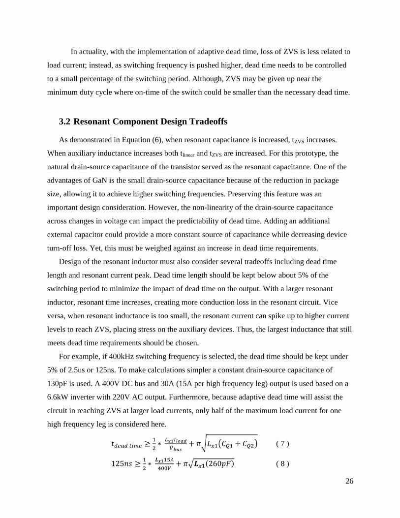
3.2 Resonant Component Design Tradeoffs
As demonstrated in Equation (6), when resonant capacitance is increased, tZVS increases.
When auxiliary inductance increases both tlinear and tZVS are increased. For this prototype, the
natural drain-source capacitance of the transistor served as the resonant capacitance. One of the
advantages of GaN is the small drain-source capacitance because of the reduction in package
size, allowing it to achieve higher switching frequencies. Preserving this feature was an
important design consideration. However, the non-linearity of the drain-source capacitance
across changes in voltage can impact the predictability of dead time. Adding an additional
external capacitor could provide a more constant source of capacitance while decreasing device
turn-off loss. Yet, this must be weighed against an increase in dead time requirements.
Design of the resonant inductor must also consider several tradeoffs including dead time
length and resonant current peak. Dead time length should be kept below about 5% of the
switching period to minimize the impact of dead time on the output. With a larger resonant
inductor, resonant time increases, creating more conduction loss in the resonant circuit. Vice
versa, when resonant inductance is too small, the resonant current can spike up to higher current
levels to reach ZVS, placing stress on the auxiliary devices. Thus, the largest inductance that still
meets dead time requirements should be chosen.
For example, if 400kHz switching frequency is selected, the dead time should be kept under
5% of 2.5us or 125ns. To make calculations simpler a constant drain-source capacitance of
130pF is used. A 400V DC bus and 30A (15A per high frequency leg) output is used based on a
6.6kW inverter with 220V AC output. Furthermore, because adaptive dead time will assist the
circuit in reaching ZVS at larger load currents, only half of the maximum load current for one
high frequency leg is considered here.
𝑡𝑑𝑒𝑎𝑑 𝑡𝑖𝑚𝑒 ≥1
2∗
𝐿𝑥1𝐼𝑙𝑜𝑎𝑑
𝑉𝑏𝑢𝑠+ 𝜋√𝐿𝑥1(𝐶𝑄1 + 𝐶𝑄2) ( 7 )
125𝑛𝑠 ≥1
2∗
𝑳𝒙𝟏15𝐴
400𝑉+ 𝜋√𝑳𝒙𝟏(260𝑝𝐹) ( 8 )

27
With these considerations, a 2.5uH auxiliary inductor is suitable, though further refinement
through prototyping is necessary for confirmation.
At such small resonant values, material constraints can also come into play. The resonant
frequency can be defined as ωres/2π (as in equation 5). Continuing with the above example, if
resonant capacitance is 130pF and resonant inductance is 2.5uH, the resonant frequency is
approximately 8.8MHz. To be fair, the true resonant current frequency could be less than that as
the current will experience both linear and resonant time periods during dead time. Yet, this
frequency range still proved difficult to find suitable ferrite cores. A summary of potential
materials is listed in Table 3.
Table 3. Core Material Options for Resonant Inductor
Name Manufacturer Ferrite Type Max Frequency
3F5 FerroxCube MnZn 5MHz
P61 Acme MnZn 6MHz
4F1 FerroxCube NiZn 10MHz
In addition, many litz wire distributors will only rate their thinnest wire “up to 2MHz”,
implying that these inductors will suffer from skin-effect related conduction losses or require
more precisely-designed PCB windings. Of course, many more factors enter into magnetics
design, but material limitations should be considered when weighing design tradeoffs.
For this prototype, P61 RM6 core samples were obtained and the resonant inductance
was boosted slightly to try to remain within the 6MHz cutoff.
3.3 Switching frequency
Switching frequency is one of the most important factors in pushing power density. Soft-
switching and GaN devices are implemented to push switching frequency while minimizing
losses. While the auxiliary snubber will increase the PCB size with additional active
components, passive components can be shrunk significantly to decrease the overall size.
Yet, dead time requirements and switching losses must be considered as well. Table 4 below
provides a snapshot of these tradeoffs: as switching frequency is increased, the required filter
inductance decreases but so does the available dead time for ZVS. For simpler comparison, the

28
table assumes that dead time constitutes 5% of the switching period and that the output filter
capacitance is 1uF with a cutoff frequency one decade below the switching frequency. Of course,
many other parameters are influential in a final design.
Table 4 Switching frequency design tradeoffs
Switching Frequency Available Dead Time Output Filter Inductance
200kHz 250ns 63.3uH
300kHz 166ns 28.1uH
400kHz 125ns 15.8uH
500kHz 100ns 10uH
For this prototype, 300kHz is selected for testing and verification of design. With further thermal
handling and efficiency optimization, this design could be pushed further to between 400kHz –
500kHz for higher power densities.
3.4 DC Bus Voltage
While the specifications in Table 2 list a 400V DC bus, the final implementation of the
inverter will include a dc/dc stage to interface with the electric vehicle batteries, provide double
line ripple rejection, and boost/buck the voltage for the dc/ac stage if necessary. Keeping the
voltage lower can allow the modulation index to be higher, allowing for optimal efficiency.
Furthermore, a lower voltage permits the use of smaller 400V or 450V rated capacitors for the
bus. However, it should be noted that the linear period of resonant current during dead time may
take longer due to the decrease in available forcing voltage. Equations 9 and 10 below show the
modulation index calculation.
𝐷𝑚𝑎𝑥 = 1 − 𝑡𝑑𝑒𝑎𝑑 𝑡𝑖𝑚𝑒 ∗ 𝑓𝑠 (9)
𝑣𝑜
𝑣𝑑𝑐= 𝑀 = 2𝐷𝑚𝑎𝑥 − 1 (10)
With a rounded-up dead time of 170ns, a switching frequency of 300kHz, and an output
voltage of 220Vrms (311Vpk), the bus voltage must be larger than 345V. For additional margin,
testing is performed between 350V-360Vdc.

29
3.5 Auxiliary Active Component Selection
The auxiliary switch is chosen to meet voltage, current, and switching requirements. While
the auxiliary switch should face fewer stresses than a main switch, the two must operate at the
same high frequency, which ultimately proves to be the largest constraint on device selection. If
the input is a maximum of 400V, with lifetime and safety de-ratings, a transistor with at least
600V blocking capability should be selected.
Across the switching period, the resonant current (and thus the current through the auxiliary
switch) spikes to just above the load current level during dead time and then remains off for the
rest of the period. This produces a relatively large peak current but an overall small rms current,
as shown in Figure 16. This makes selecting a transistor with the proper current rating somewhat
challenging as most specify a maximum continuous current while being able to handle
significantly larger pulse currents. Furthermore, because the auxiliary rms current is low, the on-
state resistance of the device selected is not a driving factor for selection.
Figure 16 Resonant Current over high frequency leg switching period
Ultimately, turn-on and turn-off of the transistor was one of the most important elements
in ensuring the device could turn on and off quickly within the small dead time window. This
factor alone eliminated the option of IGBTs. While Si-MOSFETs have significantly faster turn-
on/off times, many still consume tens of nanoseconds. Switching losses will also be the majority
of losses for these auxiliary devices and Coss, Eon/Eoff should be considered.
GaN System’s GS66508P is chosen as the auxiliary switch. It is rated for 650VDS, 30A
continuous current, 50mΩ drain-source on resistance, and rise and fall times of under 6ns. For
cost savings, a silicon MOSFET could also be used here.

30
Auxiliary diodes must conform to the same criteria as the auxiliary switch in terms of
blocking voltage and current handling. Like GaN, SiC offers zero reverse recovery, minimizing
switching loss. The Cree Sic C3D1P7060Q 600V, 1.7A rated Schottky diode is selected for all
four auxiliary diodes. Again, though the stated current rating is small, the diode also specifies
that its peak forward current pulse rating is 40A for 10us – both this current and time duration
are larger than our application will require. This diode also has an attractive small QFN package
size, minimizing parasitic capacitance and reducing the impact of additional auxiliary
components on PCB size.
3.6 Main Switch Selection for High Frequency Legs
The main switch is chosen to meet voltage, current, and switching requirements of the
interleaved inverter high frequency legs. These switches must handle the main power of the
inverter. At 6.6kW and 220Vac output, the total output rms current will be 30A. Ideally, this
current is shared by the two interleaved legs so each transistor must handle 15Arms. A small on-
state resistance will help reduce conduction loss. The minimum voltage rating of the device
should be 600V.
While previously there were very few high-voltage GaN devices available with many
proving unreliable or hard to work with, the technology is beginning to mature and more devices
with more voltages from more companies are beginning to emerge. In 2014, GaN Systems
became the first company to release a 650V rated GaN enhancement mode transistor. Their
unique method of manufacturing significantly reduced parasitic inductance for reduced noise
when switching. This project chose GS66516T 650V, 60A, 25mΩ E-mode transistor. This same
device was chosen for FEEC’s entry into the Little Box Challenge and survived 100 hours of
testing for both our team and the first place finisher’s.
Importantly, this device’s thermal pad is on the top of the package. Because the package is so
thin, all main switches can be attached to the bottom of the PCB and directly connected to a
larger heat sink while gating and other components populate the top of the PCB. At the peak
power of 6.6kW, each transistor must dissipate 5.6W of loss, which may prove difficult for such
a small package. Direct heat-sinking to spread the heat will be crucial.

31
3.7 Challenges in Driving GaN
One challenge in using GaN was design of the gate-driving circuit. Fast switching transition
noise coupled with parasitics can interfere with the control circuit, at time falsely turning on or
off the transistor. To combat this in FEEC’s entry to the Little Box Challenge, a Silicon Lab
Si8261BAC driver and a custom-designed 12V to 7V isolated power supply was used for each
device. An opto-coupler based gated driver is good for common mode noise immunity, but it
occupies a lot of space and introduces propagation delay. The Silicon Lab gate driver chip
instead employs an LED emulator that mimics the operation of a traditional optocoupler but
within a smaller volume and with shorter delays.
Yet, even with these features, it was found that the false turn-on/off persisted. Thus, a new
configuration is set up between the PWM signal of the dsp and the input to the gate driver chip.
This operation is shown in Figure 17 and Figure 18 and is originally described by the creator in
[8].
Figure 17. Equivalent electrical configuration of Silicon Labs gate driver signal input
Figure 18. Layout for added reliability of gate drive circuit
The DSP PWM signals A and B are used to drive a half-bridge with complementary
switching. Thus, when gate signal A is high, B must be low and vice versa. Thus, in Figure 18,
when the EPWM1A signal is high, the EPWM1B signal must be low and the gate driver U4 is
enabled with positive voltage. When EPWM1B is high and EPWM1A is low, U4 is disabled

32
with negative voltage and the reverse diode of U4, shown in Figure 17, conducts the reverse
current. The output pins Vo on U4 then connect to turn-on/off resistors and then to G1. While
two PWM signals are input into the circuit for error reduction, only one transistor is driven with
each gate drive circuit. Compared to the original design where K is connected to ground, this
method has proven to be more reliable.
Figure 19 shows the gating and transistor layout on the PCB for the Little Box Challenge. To
minimize noise and parasitics, top and bottom switches within a half-bridge leg should be placed
as close together as possible. The gate drive signal should also be placed as close to the gate as
possible, with any potential ground loops shrunk in length.
Figure 19 Gating and Switch layout for Little Box Challenge PCB
The GaN Systems device requires a gate voltage of between 6.5V-7V, which proves
complicated to achieve as traditional gate power supplies are not available at that voltage, not
isolated, or not precise enough. Too small a gate voltage and the transistor is not fully turned on;

33
too large a gate voltage and the transistor can fail. For the little box challenge, custom isolated
12V to 7V power supplies were created (shown in Figure 19) that provided power for each
transistor.
For the eight GaN transistors used in the two high frequency legs for the soft-switching
topology introduced in section 2, the volume of eight isolated power supplies began to become
too large. A solution was found in a newly released GaN Systems evaluation board’s schematic,
shown in Figure 20. A bootstrap gate driver is a common solution for a high-side switch where
the source pin is not connected to ground and a floating ground must be used for the associated
power supply and gate driver. When the bottom transistor is on, the source pin of the top switch
is pulled to ground and a capacitor is charged to the gate voltage. When the bottom transistor is
turned off and the top switch is signaled to turn on, the capacitor discharges to provide a voltage
to the gate driver while a diode blocks any current from flowing back to the charging source.
Because of the variable nature of a voltage source being a discharging capacitor, this option
would normally not be precise enough to reliably drive a GaN switch. Cleverly, the evaluation
board solves this issue by bootstrapping a small IC buck converter with internal comparator to
reliably supply the desired gate voltage despite fluctuations in the input voltage.
Figure 20. Modified bootstrap circuit for GaN transistor gate voltage supply

34
The designed prototype combines these two approaches by using an isolated power supply
for each leg of the inverter and a modified bootstrap circuit for the high-side switches within that
leg. This method has proven to be just as reliable while consuming less space. The modified
bootstrap method also allows for a greater level of control and freedom when selecting a precise
gate drive voltage. This allows the designer to both better protect the GaN transistor while
ensuring full turn-on.
3.8 Main Switch Selection for Low Frequency Leg
The low frequency leg is much more simplistic in design. At 60Hz, switching losses are
minimal. However, this leg must bear the full power current load of 30A. Infineon’s
IPW65R019C7 is selected for its low on-state resistance of 17mΩ. This silicon MOSFET is rated
for 650V and 75A. Yet at full power, a single TO-247 switch would have to dissipate at least
15W of loss. To assist with thermal handling and improve efficiency, two Infineon MOSFETs
are placed in parallel to cut the conduction loss in half. To further aid in thermal dissipation, the
four MOSFETs are hung off the edge of the PC board and directly attached to the same heatsink
as the main switches on the high frequency leg.
3.9 Output Filter
The output inductor-capacitor low pass filter takes in the unipolar square wave, filters out the
switching frequency and its harmonics, and outputs a smooth AC waveform. As in Table 4, the
corner frequency of the filter can be first designed as one decade below the switching frequency.
At heart, greater power density comes from pushing this corner frequency to higher frequencies
and reducing the size of the filter. Using GaN, implementing ZVS, and pushing the switching
frequency to hundreds of kHz was all implemented in an effort to shrink the volume of bulky
passive components.
Equation 11 below summarizes the relationship between the output filter values and the
cutoff frequency. For the capacitance, surface mount ceramic or film capacitors are preferred
over bulkier or less reliable other materials. For now, 1uF is chosen as either a standard value of
film capacitor could be used or ten 0.1uF 650 COG could be placed in parallel on the PCB.

35
While film capacitors are attractive because of their reliability and the safeguard of their fail as
open circuit, ceramic capacitors are smaller in size and can be easily surface mounted to the
PCB.
𝑓𝑐 =1
2𝜋√𝐿𝑜𝐶𝑜 (11)
Thus, assuming a corner frequency of one decade below the switching frequency, the output
filter inductor should be 28.1uF. Each output inductor of the two high frequency legs would need
to be this inductance. In testing, this value can be further refined. For example, having a larger
current ripple could reduce zvs time as the auxiliary current would not have to charge to as high
of a load current. Harmonic noise requirements and efficiency should also be considered.
Unipolar modulation and interleaving should reduce filtering requirements.

36
4 Design Summary
A prototype was constructed to verify the design. The input bus voltage is 350V DC and
400/450V DC electrolytic capacitors are used in lieu of the dc/dc stage for double-line ripple
suppression. The inverter is designed for 6.6kW with 220V AC output with a switching
frequency of 300kHz.
Table 5. Summary of prototype design
Power level 6.6kW
Input DC Voltage 350V
Output AC Voltage 220V
Switching Frequency 300kHz
Main High Frequency switch 650V GaN MOSFET
Auxiliary switch 650V GaN MOSFET
Auxiliary Diode 1.7A SiC Schottky
Low Frequency Leg switch 650V Si MOSFET
Auxiliary inductor 3uH in P61 RM6 core
Output inductor 24uH in 3F3 RM12 core
4.1 Hardware Test Setup
With the components of Table 5, a PCB is designed and built to test the interleaved auxiliary
resonant inverter. The PCB comprised of four layers of three-ounce copper for better current
handling capability. Only the main GaN switches were mounted to the bottom of the PCB while
the remaining components were mounted to the top of the PCB. Power components maintained a
clear gap between the low voltage gating. High current areas were given large traces interlaced
with one another such that most high power areas run in parallel across three or all of the four
layers. To reduce parasitic inductance, high and low side switches were placed close to one
another. The PCB design and populated board for testing are shown in Figure 21 and Figure 22,
respectively. For sensor processing, fault detection, and gate control, a second in-house-designed
board is attached to the main power PCB with a TI DSP TMS320F28069.

37
Figure 21 Altium PC Board layout
Figure 22. Assembled prototype for testing

38
4.2 Soft-switching
As shown in Figure 23, the red curve represents drain-source voltage starting at 350V before
the auxiliary resonant current discharges VDS to 0V. While there was some noise at the gate
(yellow curve), possibly coupling noise from the probe itself, the gate does not turn on until after
the voltage is drained, achieving ZVS. The resonant current begins at 0A and returns there
shortly after the end of the dead time period, ensuring ZCS for the auxiliary switches.
Figure 23. Auxiliary resonant circuit assists main switch to achieve ZVS
This result confirms the operation principles of the auxiliary soft switching topology
described in section 2 of this paper.
4.3 Power Density
Achieving soft switching required doubling the number of MOSFETs, adding several diodes,
and two auxiliary inductors. Yet the extra diodes and transistors are active elements that are
small and continue to decrease in size while increasing in functionality. Thus, power density
relies on minimization of the output filter, keeping the auxiliary inductor small, form-factor
awareness, and simplified thermal management.
Figure 22 shows the assembled prototype. The DSP PCB, current sensor, and input
capacitors are all 1” tall. The resonant inductor is small enough to be directly anchored to the
board. The output inductors will be placed on a platform sitting on top of the low profile areas of
the PCB. The low frequency devices are hung over the side to provide easier access to the heat
sink. The main high frequency switches are “top-cooled” and are attached to the bottom of the
VDS=350V
ILo1 Vgate: 0 to 7V
ILx1
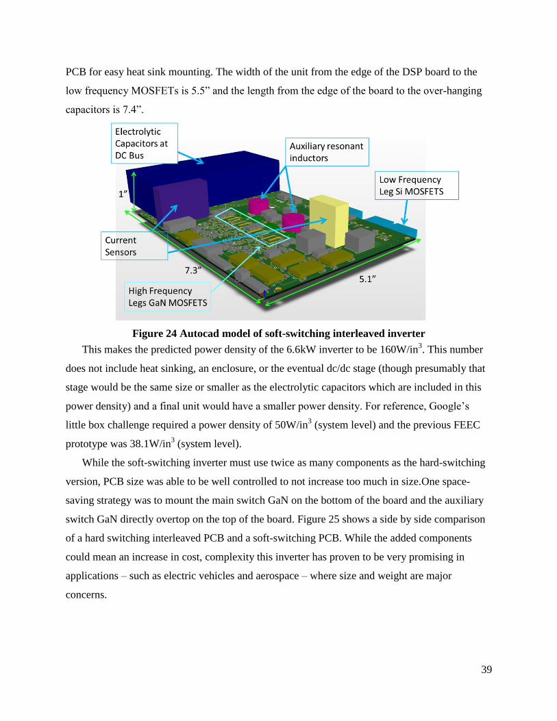
39
PCB for easy heat sink mounting. The width of the unit from the edge of the DSP board to the
low frequency MOSFETs is 5.5” and the length from the edge of the board to the over-hanging
capacitors is 7.4”.
Figure 24 Autocad model of soft-switching interleaved inverter
This makes the predicted power density of the 6.6kW inverter to be 160W/in3. This number
does not include heat sinking, an enclosure, or the eventual dc/dc stage (though presumably that
stage would be the same size or smaller as the electrolytic capacitors which are included in this
power density) and a final unit would have a smaller power density. For reference, Google’s
little box challenge required a power density of 50W/in3 (system level) and the previous FEEC
prototype was 38.1W/in3 (system level).
While the soft-switching inverter must use twice as many components as the hard-switching
version, PCB size was able to be well controlled to not increase too much in size.One space-
saving strategy was to mount the main switch GaN on the bottom of the board and the auxiliary
switch GaN directly overtop on the top of the board. Figure 25 shows a side by side comparison
of a hard switching interleaved PCB and a soft-switching PCB. While the added components
could mean an increase in cost, complexity this inverter has proven to be very promising in
applications – such as electric vehicles and aerospace – where size and weight are major
concerns.

40
Figure 25 PCB size for hard switching topology (left) and soft switching topology (right)
4.4 Zero Crossing Issue
Unfortunately, an issue emerged that halted further power handling testing, efficiency
examinations, and design parameter refinement. When the output AC waveforms crossed zero
from either positive to negative or negative to positive, significant ringing occurs. This noise is
short-lived but large – often larger than the output waveform itself. At even low power and
voltage input, a protection circuit was consistently tripped, the zero crossing spike so significant
the protection believed it was a shoot-through event. While perhaps the protection level could
simply be boosted (it is already at twice the rated current), this could leave the sensitive (and
pricey) GaN devices vulnerable while doing little to solve the real issue at hand.
First, ZVS and full-voltage handling capabilities were confirmed by keeping duty cycle
constant and creating a DC output voltage instead of the desired AC waveform. The zero
crossing spiking is also present in the hard switching interleaved inverter and does not seem to be
impacted by the soft-switching circuit.
It must be noted that at the zero crossing, several drastic gating signal changes are made in
one moment. A low frequency device turns off, followed by dead time and the other low
frequency device turning on. The main switches of the interleaved high frequency legs change
from the minimum duty cycle to a complementary signal at the largest duty cycle. This makes it

41
difficult to determine the origin of this spiking: unsynchronized switching, the change from low
to high duty cycle and vice versa of the high frequency main switches, the drain-source
capacitance of the low frequency leg resonating during dead time, or that with zero load current,
spikes occur to quickly charge the low frequency leg drain-capacitance during turn-on.
First, the gate signals were fully synchronized at the zero crossing to test if this was the
origin of the spiking. Synchronization requires more complex code because all of the main
switching signals must be signaled to turn off together, despite differences in phase, remain off
for the duration of the dead time, and then turn on together and return to their proper duty cycle
and phase. The resulting synchronized gate signals are shown in Figure 26.
(a) Turn-off of top low frequency switch
(b) Turn-on of top low frequency switch
Figure 26 Synchronized turn-on and turn-off of gate signals at zero crossing points.
The yellow waveform is the top low frequency switch, blue is the bottom low frequency
switch, red the top main switch of the first high frequency leg, and the green is the top main
switch of the second high frequency leg
When compared with other strategies such as allowing the main switches to continue
turning on/off during dead time, turning main switches on/off slightly before the low frequency’s
signal to turn on/off, etc, synchronizes switching showed the most improvement. Yet, the
resonance remained, as shown in Figure 27. Though the image makes the noise appear somewhat
small, the input voltage was only 10V and the input current spiked to more than double the peak
of the rest of the waveform. As input voltage and output power increased, this relationship
remained continued to harmful levels.
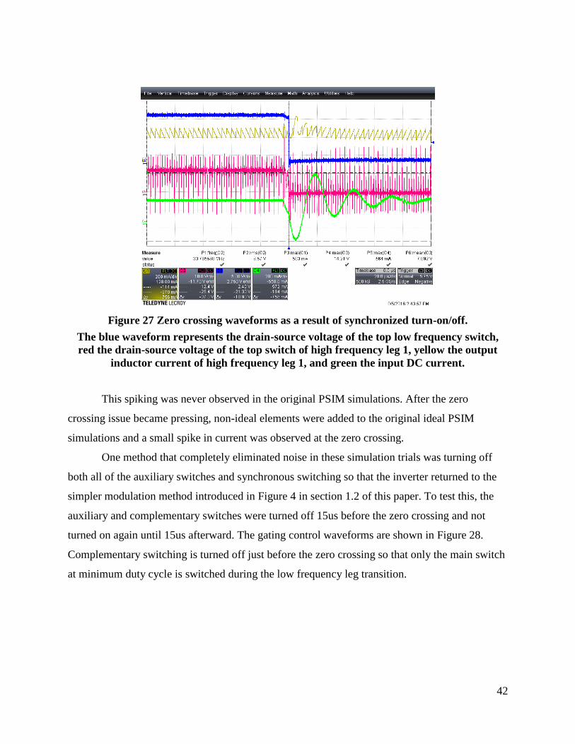
42
Figure 27 Zero crossing waveforms as a result of synchronized turn-on/off.
The blue waveform represents the drain-source voltage of the top low frequency switch,
red the drain-source voltage of the top switch of high frequency leg 1, yellow the output
inductor current of high frequency leg 1, and green the input DC current.
This spiking was never observed in the original PSIM simulations. After the zero
crossing issue became pressing, non-ideal elements were added to the original ideal PSIM
simulations and a small spike in current was observed at the zero crossing.
One method that completely eliminated noise in these simulation trials was turning off
both all of the auxiliary switches and synchronous switching so that the inverter returned to the
simpler modulation method introduced in Figure 4 in section 1.2 of this paper. To test this, the
auxiliary and complementary switches were turned off 15us before the zero crossing and not
turned on again until 15us afterward. The gating control waveforms are shown in Figure 28.
Complementary switching is turned off just before the zero crossing so that only the main switch
at minimum duty cycle is switched during the low frequency leg transition.

43
Figure 28 Modified gating waveforms at zero crossing. The yellow and red waveforms
control the low frequency legs and the green and blue waveforms control the main switches
of a single high frequency leg.
Unfortunately, while still smaller than other methods tried, the zero crossing issue
remained at a level relatively unchanged from the previous configuration in Figure 27, as shown
in Figure 29 and Figure 30.
Figure 29 Spikes in current remain despite the simplified gating around the zero crossing
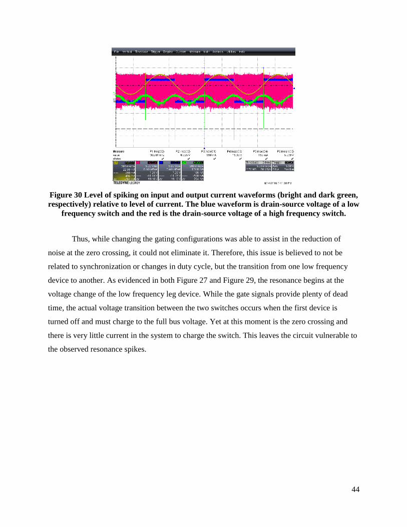
44
Figure 30 Level of spiking on input and output current waveforms (bright and dark green,
respectively) relative to level of current. The blue waveform is drain-source voltage of a low
frequency switch and the red is the drain-source voltage of a high frequency switch.
Thus, while changing the gating configurations was able to assist in the reduction of
noise at the zero crossing, it could not eliminate it. Therefore, this issue is believed to not be
related to synchronization or changes in duty cycle, but the transition from one low frequency
device to another. As evidenced in both Figure 27 and Figure 29, the resonance begins at the
voltage change of the low frequency leg device. While the gate signals provide plenty of dead
time, the actual voltage transition between the two switches occurs when the first device is
turned off and must charge to the full bus voltage. Yet at this moment is the zero crossing and
there is very little current in the system to charge the switch. This leaves the circuit vulnerable to
the observed resonance spikes.

45
5 Conclusion
The setback in managing the zero crossing must be further investigated and solved. While
this paper focused on managing gate signal timing, perhaps other avenues of control such as
hardware changes or closing the control loop may prove more fruitful.
If the zero crossing issue is solved, this topology shows incredible promise for pushing
inverters to higher densities. Because several parameters could not be further refined through
testing, several avenues of future work exist with this topology. Switching frequency can be
pushed even further to 500kHz, though the impact on efficiency and available dead time should
be closely monitored. Optimizing the auxiliary resonant inductor/capacitor relationship for
achieving ZVS also requires further study. Finally, the combination of high switching frequency
and soft-switching should minimize the necessary size of EMI filters, but must be tested and
compared with the hard switching version.
A novel interleaved, soft-switching inverter is proposed. The mechanisms of interleaving are
discussed as well as the decision making process for finding a soft-switching solution. The
resonant circuit is analyzed to optimize the resonant components, find a suitable dead time
length, and achieve ZVS across load conditions. Finally, a 6.6kW prototype was introduced that
could reach 160W/in3 power density.

46
6 Citations
[1] Z. Liu, X. Huang, W. Zhang, F. C. Lee, and Q. Li, "Evaluation of high-voltage cascode GaN
HEMT in different packages," in 2014 IEEE Applied Power Electronics Conference and
Exposition - APEC 2014, 2014, pp. 168-173.
[2] T. Warren. (2016). Tesla has received almost 400,000 preorders for the Model 3.
[3] B. Howard. (2016). Model E: Now Ford plans a 200-mile electric vehicle.
[4] Developing Infrastructure to Charge Plug-In Electric Vehicles.
[5] Z. Shahan. (2015). Electric Car Charging 101 — Types of Charging, Charging Networks,
Apps, & More!
[6] Electric Vehicle Charging Infrastructure.
[7] COOLER-SIZED ISN'T COOL. Available: https://www.littleboxchallenge.com/
[8] L. Zhang, R. Born, X. Zhao, and J. S. Lai, "A high efficiency inverter design for Google little
box challenge," in Wide Bandgap Power Devices and Applications (WiPDA), 2015 IEEE 3rd
Workshop on, 2015, pp. 319-322.
[9] J. Dominic, "Comparison and Design of High Efficiency Microinverters for Photovoltaic
Applications," M.S., Electrical and Computer Engineering, Virginia Tech, 2015.
[10] D. M. Divan and G. Skibinski, "Zero-switching-loss inverters for high-power
applications," IEEE Transactions on Industry Applications, vol. 25, pp. 634-643, 1989.
[11] Q. Zhang, H. Hu, D. Zhang, X. Fang, Z. J. Shen, and I. Bartarseh, "A Controlled-Type
ZVS Technique Without Auxiliary Components for the Low Power DC/AC Inverter," IEEE
Transactions on Power Electronics, vol. 28, pp. 3287-3296, 2013.
[12] W. Chien-Ming, "Nonlinear-controlled strategy for soft-switched series-resonant DC/AC
inverter without auxiliary switches," IEEE Transactions on Power Electronics, vol. 18, pp.
764-774, 2003.
[13] E. Faraci, "Design of a Resonant Snubber Inverter for
Photovoltaic Inverter Systems," M.S., Electrical and Computer Engineering, Virginia Tech,
2014.
[14] J. S. Lai, R. W. Young, D. Chen, M. B. Scudiere, G. W. Ott, C. P. White, et al.,
"Resonant snubber inverter," ed: Google Patents, 1997.

47
[15] J. S. Lai, R. W. Young, G. W. Ott, C. P. White, J. W. McKeever, and D. Chen, "A novel
resonant snubber based soft-switching inverter," in Applied Power Electronics Conference
and Exposition, 1995. APEC '95. Conference Proceedings 1995., Tenth Annual, 1995, pp.
797-803 vol.2.
[16] I. Barbi and D. C. Martins, "A true PWM zero-voltage switching pole, with very low
additional RMS current stress," in Power Electronics Specialists Conference, 1991. PESC
'91 Record., 22nd Annual IEEE, 1991, pp. 261-267.
[17] J. s. Lai, J. Zhang, H. Yu, and H. Kouns, "Source and Load Adaptive Design for a High-
Power Soft-Switching Inverter," IEEE Transactions on Power Electronics, vol. 21, pp. 1667-
1675, 2006.
[18] K. M. Smith and K. M. Smedley, "A comparison of voltage-mode soft-switching
methods for PWM converters," IEEE Transactions on Power Electronics, vol. 12, pp. 376-
386, 1997.
[19] Y. Xiaoming and I. Barbi, "Analysis, designing, and experimentation of a transformer-
assisted PWM zero-voltage switching pole inverter," IEEE Transactions on Power
Electronics, vol. 15, pp. 72-82, 2000.
[20] B. Chen, J. S. Lai, C. L. Chen, W. Yu, N. Kees, C. Zheng, et al., "Design and
optimization of 99% CEC efficiency soft-switching photovoltaic inverter," in Applied Power
Electronics Conference and Exposition (APEC), 2013 Twenty-Eighth Annual IEEE, 2013,
pp. 946-951.
[21] W. Yu, J. S. Lai, and S. Y. Park, "An Improved Zero-Voltage Switching Inverter Using
Two Coupled Magnetics in One Resonant Pole," IEEE Transactions on Power Electronics,
vol. 25, pp. 952-961, 2010.
[22] A. Reibel, "Little Box Challenge Technical Approach Document," 2015.