SNLS130C – MARCH 1999– REVISED MARCH 2013 … · · 2016-09-12 SNLS130C – MARCH 1999–...
27
DS90CR285, DS90CR286 www.ti.com SNLS130C – MARCH 1999 – REVISED MARCH 2013 DS90CR285/DS90CR286 +3.3V Rising Edge Data Strobe LVDS 28-Bit Channel Link-66 MHz Check for Samples: DS90CR285, DS90CR286 1FEATURES DESCRIPTION The DS90CR285 transmitter converts 28 bits of 2• Single +3.3V Supply LVCMOS/LVTTL data into four LVDS (Low Voltage • Chipset (Tx + Rx) Power Consumption <250 Differential Signaling) data streams. A phase-locked mW (typ) transmit clock is transmitted in parallel with the data • Power-Down Mode (<0.5 mW total) streams over a fifth LVDS link. Every cycle of the transmit clock 28 bits of input data are sampled and • Up to 231 Megabytes/sec Bandwidth transmitted. The DS90CR286 receiver converts the • Up to 1.848 Gbps Data Throughput LVDS data streams back into 28 bits of • Narrow Bus Reduces Cable Size LVCMOS/LVTTL data. At a transmit clock frequency of 66 MHz, 28 bits of TTL data are transmitted at a • 290 mV Swing LVDS Devices for Low EMI rate of 462 Mbps per LVDS data channel. Using a 66 • +1V Common Mode Range (Around +1.2V) MHz clock, the data throughput is 1.848 Gbit/s (231 • PLL Requires no External Components Mbytes/s). • Both Devices are Offered in a Low Profile 56- The multiplexing of the data lines provides a Lead TSSOP Package substantial cable reduction. Long distance parallel • Rising Edge Data Strobe single-ended buses typically require a ground wire per active signal (and have very limited noise • Compatible with TIA/EIA-644 LVDS Standard rejection capability). Thus, for a 28-bit wide data and • ESD Rating > 7 kV one clock, up to 58 conductors are required. With the • Operating Temperature: −40°C to +85°C Channel Link chipset as few as 11 conductors (4 data pairs, 1 clock pair and a minimum of one ground) are needed. This provides a 80% reduction in required cable width, which provides a system cost savings, reduces connector physical size and cost, and reduces shielding requirements due to the cables' smaller form factor. The 28 LVCMOS/LVTTL inputs can support a variety of signal combinations. For example, seven 4-bit nibbles or three 9-bit (byte + parity) and 1 control. 1 Please be aware that an important notice concerning availability, standard warranty, and use in critical applications of Texas Instruments semiconductor products and disclaimers thereto appears at the end of this data sheet. 2All trademarks are the property of their respective owners. PRODUCTION DATA information is current as of publication date. Copyright © 1999–2013, Texas Instruments Incorporated Products conform to specifications per the terms of the Texas Instruments standard warranty. Production processing does not necessarily include testing of all parameters.
Transcript of SNLS130C – MARCH 1999– REVISED MARCH 2013 … · · 2016-09-12 SNLS130C – MARCH 1999–...

DS90CR285, DS90CR286
www.ti.com SNLS130C –MARCH 1999–REVISED MARCH 2013
DS90CR285/DS90CR286 +3.3V Rising Edge Data Strobe LVDS 28-Bit Channel Link-66 MHzCheck for Samples: DS90CR285, DS90CR286
1FEATURES DESCRIPTIONThe DS90CR285 transmitter converts 28 bits of
2• Single +3.3V SupplyLVCMOS/LVTTL data into four LVDS (Low Voltage
• Chipset (Tx + Rx) Power Consumption <250 Differential Signaling) data streams. A phase-lockedmW (typ) transmit clock is transmitted in parallel with the data
• Power-Down Mode (<0.5 mW total) streams over a fifth LVDS link. Every cycle of thetransmit clock 28 bits of input data are sampled and• Up to 231 Megabytes/sec Bandwidthtransmitted. The DS90CR286 receiver converts the
• Up to 1.848 Gbps Data Throughput LVDS data streams back into 28 bits of• Narrow Bus Reduces Cable Size LVCMOS/LVTTL data. At a transmit clock frequency
of 66 MHz, 28 bits of TTL data are transmitted at a• 290 mV Swing LVDS Devices for Low EMIrate of 462 Mbps per LVDS data channel. Using a 66• +1V Common Mode Range (Around +1.2V) MHz clock, the data throughput is 1.848 Gbit/s (231
• PLL Requires no External Components Mbytes/s).• Both Devices are Offered in a Low Profile 56- The multiplexing of the data lines provides a
Lead TSSOP Package substantial cable reduction. Long distance parallel• Rising Edge Data Strobe single-ended buses typically require a ground wire
per active signal (and have very limited noise• Compatible with TIA/EIA-644 LVDS Standardrejection capability). Thus, for a 28-bit wide data and
• ESD Rating > 7 kV one clock, up to 58 conductors are required. With the• Operating Temperature: −40°C to +85°C Channel Link chipset as few as 11 conductors (4 data
pairs, 1 clock pair and a minimum of one ground) areneeded. This provides a 80% reduction in requiredcable width, which provides a system cost savings,reduces connector physical size and cost, andreduces shielding requirements due to the cables'smaller form factor.
The 28 LVCMOS/LVTTL inputs can support a varietyof signal combinations. For example, seven 4-bitnibbles or three 9-bit (byte + parity) and 1 control.
1
Please be aware that an important notice concerning availability, standard warranty, and use in critical applications ofTexas Instruments semiconductor products and disclaimers thereto appears at the end of this data sheet.
2All trademarks are the property of their respective owners.
PRODUCTION DATA information is current as of publication date. Copyright © 1999–2013, Texas Instruments IncorporatedProducts conform to specifications per the terms of the TexasInstruments standard warranty. Production processing does notnecessarily include testing of all parameters.

DS90CR285, DS90CR286
SNLS130C –MARCH 1999–REVISED MARCH 2013 www.ti.com
Block Diagram
Figure 1. DS90CR285 - 56-Lead TSSOP Figure 2. DS90CR285 - 56-Lead TSSOPSee Package Number DGG0056A See Package Number DGG0056A
Pin Diagrams for TSSOP Packages
Figure 3. DS90CR285 Figure 4. DS90CR286See Package Number DGG (R-PDSO-G56) See Package Number DGG (R-PDSO-G56)
2 Submit Documentation Feedback Copyright © 1999–2013, Texas Instruments Incorporated
Product Folder Links: DS90CR285 DS90CR286

DS90CR285, DS90CR286
www.ti.com SNLS130C –MARCH 1999–REVISED MARCH 2013
Typical Application
These devices have limited built-in ESD protection. The leads should be shorted together or the device placed in conductive foamduring storage or handling to prevent electrostatic damage to the MOS gates.
Absolute Maximum Ratings (1) (2)
Supply Voltage (VCC) −0.3V to +4V
CMOS/TTL Input Voltage −0.3V to (VCC + 0.3V)
CMOS/TTL Output Voltage −0.3V to (VCC + 0.3V)
LVDS Receiver Input Voltage −0.3V to (VCC + 0.3V)
LVDS Driver Output Voltage −0.3V to (VCC + 0.3V)
LVDS Output Short Circuit Duration Continuous
Junction Temperature +150°C
Storage Temperature −65°C to +150°C
Lead Temperature (Soldering, 4 sec.) +260°C
Solder Reflow Temperature Maximum Package Power DS90CR285MTD 1.63 WDissipation @ +25°C DS90CR286MTD 1.61 W
Package Derating: DS90CR285MTD 12.5 mW/°C above +25°C
DS90CR286MTD 12.4 mW/°C above +25°C
ESD Rating (HBM, 1.5 kΩ, 100 pF) > 7 kV
(1) “Absolute Maximum Ratings” are those values beyond which the safety of the device cannot be guaranteed. They are not meant toimply that the device should be operated at these limits. “Electrical Characteristics” specify conditions for device operation.
(2) If Military/Aerospace specified devices are required, please contact the TI Sales Office/ Distributors for availability and specifications.
Recommended Operating ConditionsMin Nom Max Units
Supply Voltage (VCC) 3.0 3.3 3.6 V
Operating Free Air Temperature (TA) −40 +25 +85 °C
Receiver Input Range 0 2.4 V
Supply Noise Voltage (VCC) 100 mVPP
Copyright © 1999–2013, Texas Instruments Incorporated Submit Documentation Feedback 3
Product Folder Links: DS90CR285 DS90CR286

DS90CR285, DS90CR286
SNLS130C –MARCH 1999–REVISED MARCH 2013 www.ti.com
Electrical CharacteristicsOver recommended operating supply and temperature ranges unless otherwise specified
Symbol Parameter Conditions Min Typ Max Units
LVCMOS/LVTTL DC SPECIFICATIONS
VIH High Level Input Voltage 2.0 VCC V
VIL Low Level Input Voltage GND 0.8 V
VOH High Level Output Voltage IOH = −0.4 mA 2.7 3.3 V
VOL Low Level Output Voltage IOL = 2 mA 0.06 0.3 V
VCL Input Clamp Voltage ICL = −18 mA −0.79 −1.5 V
IIN Input Current VIN = VCC, GND, 2.5V or 0.4V ±5.1 ±10 μA
IOS Output Short Circuit Current VOUT = 0V −60 −120 mA
LVDS DRIVER DC SPECIFICATIONS
VOD Differential Output Voltage RL = 100Ω 250 290 450 mV
ΔVOD Change in VOD between Complimentary Output 35 mVStates
VOS Offset Voltage (1) 1.125 1.25 1.375 V
ΔVOS Change in VOS between Complimentary Output 35 mVStates
IOS Output Short Circuit Current VOUT = 0V, RL = 100Ω −3.5 −5 mA
IOZ Output TRI-STATE Current PWR DWN = 0V, ±1 ±10 μA
VOUT = 0V or VCC
LVDS RECEIVER DC SPECIFICATIONS
VTH Differential Input High Threshold VCM = +1.2V +100 mV
VTL Differential Input Low Threshold −100 mV
IIN Input Current VIN = +2.4V, VCC = 3.6V ±10 μA
VIN = 0V, VCC = 3.6V ±10 μA
TRANSMITTER SUPPLY CURRENT
ICCTW Transmitter Supply Current Worst Case (with RL = 100Ω, f = 32.5 MHz 31 45 mALoads) CL = 5 pF, f = 37.5 MHz 32 50 mA
Worst Case Patternf = 66 MHz 37 55 mA(Figure 5 Figure 6)
, TA = −10°C to +70°C
RL = 100Ω, f = 40 MHz 38 51 mACL = 5 pF, f = 66 MHz 42 55 mAWorst Case Pattern(Figure 5 Figure 6), TA = −40°C to +85°C
ICCTZ Transmitter Supply Current Power Down PWR DWN = Low 10 55 μADriver Outputs in TRI-STATEunder Powerdown Mode
RECEIVER SUPPLY CURRENT
ICCRW Receiver Supply Current Worst Case CL = 8 pF, f = 32.5 MHz 49 65 mAWorst Case Pattern f = 37.5 MHz 53 70 mA(Figure 5 Figure 7)
f = 66 MHz 78 105 mA, TA = −10°C to +70°C
CL = 8 pF, f = 40 MHz 55 82 mAWorst Case Pattern f = 66 MHz 78 105 mA(Figure 5 Figure 7), TA = −40°C to +85°C
ICCRZ Receiver Supply Current Power Down PWR DWN = Low 10 55 μAReceiver Outputs Stay Low duringPowerdown Mode
(1) VOS previously referred as VCM.
4 Submit Documentation Feedback Copyright © 1999–2013, Texas Instruments Incorporated
Product Folder Links: DS90CR285 DS90CR286

DS90CR285, DS90CR286
www.ti.com SNLS130C –MARCH 1999–REVISED MARCH 2013
Transmitter Switching CharacteristicsOver recommended operating supply and −40°C to +85°C ranges unless otherwise specified
Symbol Parameter Min Typ Max Units
LLHT LVDS Low-to-High Transition Time (Figure 6) 0.5 1.5 ns
LHLT LVDS High-to-Low Transition Time (Figure 6) 0.5 1.5 ns
TCIT TxCLK IN Transition Time (Figure 8) 5 ns
TCCS TxOUT Channel-to-Channel Skew (Figure 9) 250 ps
TPPos0 Transmitter Output Pulse Position for Bit0 f = 40 MHz −0.4 0 0.4 ns(1)(Figure 20)
TPPos1 Transmitter Output Pulse Position for Bit1 3.1 3.3 4.0 ns
TPPos2 Transmitter Output Pulse Position for Bit2 6.5 6.8 7.6 ns
TPPos3 Transmitter Output Pulse Position for Bit3 10.2 10.4 11.0 ns
TPPos4 Transmitter Output Pulse Position for Bit4 13.7 13.9 14.6 ns
TPPos5 Transmitter Output Pulse Position for Bit5 17.3 17.6 18.2 ns
TPPos6 Transmitter Output Pulse Position for Bit6 21.0 21.2 21.8 ns
TPPos0 Transmitter Output Pulse Position for Bit0 f = 66 MHz −0.4 0 0.3 ns(2)(Figure 20)
TPPos1 Transmitter Output Pulse Position for Bit1 1.8 2.2 2.5 ns
TPPos2 Transmitter Output Pulse Position for Bit2 4.0 4.4 4.7 ns
TPPos3 Transmitter Output Pulse Position for Bit3 6.2 6.6 6.9 ns
TPPos4 Transmitter Output Pulse Position for Bit4 8.4 8.8 9.1 ns
TPPos5 Transmitter Output Pulse Position for Bit5 10.6 11.0 11.3 ns
TPPos6 Transmitter Output Pulse Position for Bit6 12.8 13.2 13.5 ns
TCIP TxCLK IN Period (Figure 10 ) 15 T 50 ns
TCIH TxCLK IN High Time (Figure 10) 0.35T 0.5T 0.65T ns
TCIL TxCLK IN Low Time (Figure 10) 0.35T 0.5T 0.65T ns
TSTC TxIN Setup to TxCLK IN (Figure 10) 2.5 ns
THTC TxIN Hold to TxCLK IN (Figure 10) 0 ns
TCCD TxCLK IN to TxCLK OUT Delay @ 25°C,VCC=3.3V (Figure 12) 3 3.7 5.5 ns
TPLLS Transmitter Phase Lock Loop Set (Figure 14) 10 ms
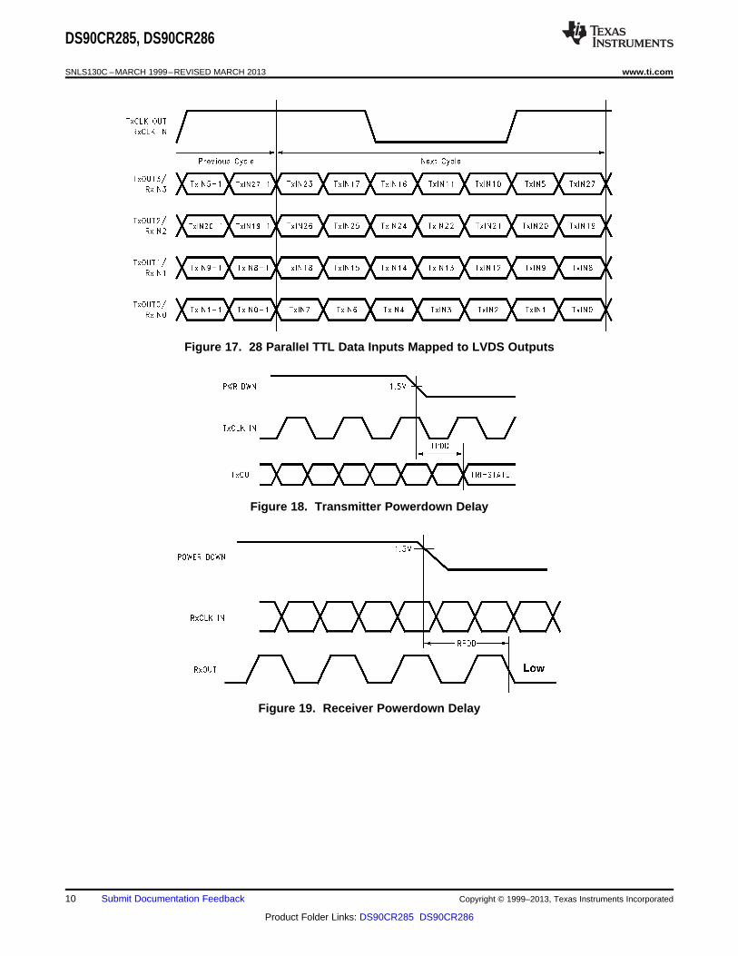
TPDD Transmitter Powerdown Delay (Figure 18) 100 ns
(1) The min. and max. are based on the actual bit position of each of the 7 bits within the LVDS data stream across PVT.(2) The min. and max. limits are based on the worst bit by applying a −400ps/+300ps shift from ideal position.
Receiver Switching CharacteristicsOver recommended operating supply and −40°C to +85°C ranges unless otherwise specified
Symbol Parameter Min Typ Max Units
CLHT CMOS/TTL Low-to-High Transition Time (Figure 7) 2.2 5.0 ns
CHLT CMOS/TTL High-to-Low Transition Time (Figure 7) 2.2 5.0 ns
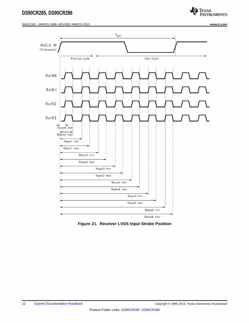
RSPos0 Receiver Input Strobe Position for Bit 0 (1)(Figure 21) f = 40 MHz 1.0 1.4 2.15 ns
RSPos1 Receiver Input Strobe Position for Bit 1 4.5 5.0 5.8 ns
RSPos2 Receiver Input Strobe Position for Bit 2 8.1 8.5 9.15 ns
RSPos3 Receiver Input Strobe Position for Bit 3 11.6 11.9 12.6 ns
RSPos4 Receiver Input Strobe Position for Bit 4 15.1 15.6 16.3 ns
RSPos5 Receiver Input Strobe Position for Bit 5 18.8 19.2 19.9 ns
RSPos6 Receiver Input Strobe Position for Bit 6 22.5 22.9 23.6 ns
(1) The min. and max. are based on the actual bit position of each of the 7 bits within the LVDS data stream across PVT.
Copyright © 1999–2013, Texas Instruments Incorporated Submit Documentation Feedback 5
Product Folder Links: DS90CR285 DS90CR286

DS90CR285, DS90CR286
SNLS130C –MARCH 1999–REVISED MARCH 2013 www.ti.com
Receiver Switching Characteristics (continued)Over recommended operating supply and −40°C to +85°C ranges unless otherwise specified
Symbol Parameter Min Typ Max Units
RSPos0 Receiver Input Strobe Position for Bit 0 (2)(Figure 21) f = 66 MHz 0.7 1.1 1.4 ns
RSPos1 Receiver Input Strobe Position for Bit 1 2.9 3.3 3.6 ns
RSPos2 Receiver Input Strobe Position for Bit 2 5.1 5.5 5.8 ns
RSPos3 Receiver Input Strobe Position for Bit 3 7.3 7.7 8.0 ns
RSPos4 Receiver Input Strobe Position for Bit 4 9.5 9.9 10.2 ns
RSPos5 Receiver Input Strobe Position for Bit 5 11.7 12.1 12.4 ns
RSPos6 Receiver Input Strobe Position for Bit 6 13.9 14.3 14.6 ns
RSKM RxIN Skew Margin (3)(Figure 22) f = 40 MHz 490 ps
f = 66 MHz 400 ps
RCOP RxCLK OUT Period (Figure 11) 15 T 50 ns
RCOH RxCLK OUT High Time (Figure 11) f = 40 MHz 6.0 10.0 ns
f = 66 MHz 4.0 6.1 ns
RCOL RxCLK OUT Low Time (Figure 11) f = 40 MHz 10.0 13.0 ns
f = 66 MHz 6.0 7.8 ns
RSRC RxOUT Setup to RxCLK OUT (Figure 11) f = 40 MHz 6.5 14.0 ns
f = 66 MHz 2.5 8.0 ns
RHRC RxOUT Hold to RxCLK OUT (Figure 11) f = 40 MHz 6.0 8.0 ns
f = 66 MHz 2.5 4.0 ns
RCCD RxCLK IN to RxCLK OUT Delay (Figure 13) f = 40 MHz 4.0 6.7 8.0 ns
f = 66 MHz 5.0 6.6 9.0 ns
RPLLS Receiver Phase Lock Loop Set (Figure 15) 10 ms
RPDD Receiver Powerdown Delay (Figure 19) 1 μs
(2) The min. and max. limits are based on the worst bit by applying a −400ps/+300ps shift from ideal position.(3) Receiver Skew Margin is defined as the valid data sampling region at the receiver inputs. This margin takes into account the transmitter
pulse positions (min and max) and the receiver input setup and hold time (internal data sampling window). This margin allows LVDSinterconnect skew, inter-symbol interference (both dependent on type/length of cable), and clock jitter less than 250 ps).
AC TIMING DIAGRAMS
Figure 5. “Worst Case” Test Pattern
6 Submit Documentation Feedback Copyright © 1999–2013, Texas Instruments Incorporated
Product Folder Links: DS90CR285 DS90CR286

DS90CR285, DS90CR286
www.ti.com SNLS130C –MARCH 1999–REVISED MARCH 2013
Figure 6. DS90CR285 (Transmitter) LVDS Output Load and Transition Times
Figure 7. DS90CR286 (Receiver) CMOS/TTL Output Load and Transition Times
Figure 8. DS90CR285 (Transmitter) Input Clock Transition Time
(1) Measurements at VDIFF = 0V
(2) TCCS measured between earliest and latest LVDS edges.
(3) TxCLK Differential Low→High Edge
Figure 9. DS90CR285 (Transmitter) Channel-to-Channel Skew
Copyright © 1999–2013, Texas Instruments Incorporated Submit Documentation Feedback 7
Product Folder Links: DS90CR285 DS90CR286

DS90CR285, DS90CR286
SNLS130C –MARCH 1999–REVISED MARCH 2013 www.ti.com
Figure 10. DS90CR285 (Transmitter) Setup/Hold and High/Low Times
Figure 11. DS90CR286 (Receiver) Setup/Hold and High/Low Times
Figure 12. DS90CR285 (Transmitter) Clock In to Clock Out Delay
Figure 13. DS90CR286 (Receiver) Clock In to Clock Out Delay
8 Submit Documentation Feedback Copyright © 1999–2013, Texas Instruments Incorporated
Product Folder Links: DS90CR285 DS90CR286

DS90CR285, DS90CR286
www.ti.com SNLS130C –MARCH 1999–REVISED MARCH 2013
Figure 14. DS90CR285 (Transmitter) Phase Lock Loop Set Time
Figure 15. DS90CR286 (Receiver) Phase Lock Loop Set Time
Figure 16. Seven Bits of LVDS in Once Clock Cycle
Copyright © 1999–2013, Texas Instruments Incorporated Submit Documentation Feedback 9
Product Folder Links: DS90CR285 DS90CR286
DS90CR285, DS90CR286
SNLS130C –MARCH 1999–REVISED MARCH 2013 www.ti.com
Figure 17. 28 ParalIeI TTL Data Inputs Mapped to LVDS Outputs
Figure 18. Transmitter Powerdown DeIay
Figure 19. Receiver Powerdown Delay
10 Submit Documentation Feedback Copyright © 1999–2013, Texas Instruments Incorporated
Product Folder Links: DS90CR285 DS90CR286

DS90CR285, DS90CR286
www.ti.com SNLS130C –MARCH 1999–REVISED MARCH 2013
Figure 20. Transmitter LVDS Output Pulse Position Measurement
Copyright © 1999–2013, Texas Instruments Incorporated Submit Documentation Feedback 11
Product Folder Links: DS90CR285 DS90CR286
DS90CR285, DS90CR286
SNLS130C –MARCH 1999–REVISED MARCH 2013 www.ti.com
Figure 21. Receiver LVDS Input Strobe Position
12 Submit Documentation Feedback Copyright © 1999–2013, Texas Instruments Incorporated
Product Folder Links: DS90CR285 DS90CR286

DS90CR285, DS90CR286
www.ti.com SNLS130C –MARCH 1999–REVISED MARCH 2013
C—Setup and Hold Time (Internal data sampling window) defined by Rspos (receiver input strobe position) min andmaxTppos—Transmitter output pulse position (min and max)RSKM ≥ Cable Skew (type, length) + Source Clock Jitter (cycle to cycle) + ISI (Inter-symbol interference)Cable Skew—typically 10 ps–40 ps per foot, media dependent
(1) Cycle-to-cycle jitter is less than 250 ps
(2) ISI is dependent on interconnect length; may be zero
Figure 22. Receiver LVDS Input Skew Margin
Copyright © 1999–2013, Texas Instruments Incorporated Submit Documentation Feedback 13
Product Folder Links: DS90CR285 DS90CR286

DS90CR285, DS90CR286
SNLS130C –MARCH 1999–REVISED MARCH 2013 www.ti.com
DS90CR285 DGG (TSSOP) Package Pin Description — Channel Link TransmitterPin Name I/O No. Description
TxIN I 28 TTL level input.
TxOUT+ O 4 Positive LVDS differential data output.
TxOUT− O 4 Negative LVDS differential data output.
TxCLK IN I 1 TTL IeveI clock input. The rising edge acts as data strobe. Pin name TxCLK IN.
TxCLK OUT+ O 1 Positive LVDS differential clock output.
TxCLK OUT− O 1 Negative LVDS differential clock output.
PWR DWN I 1 TTL level input. Assertion (low input) TRI-STATES the outputs, ensuring low current at power down.
VCC I 4 Power supply pins for TTL inputs.
GND I 5 Ground pins for TTL inputs.
PLL VCC I 1 Power supply pin for PLL.
PLL GND I 2 Ground pins for PLL.
LVDS VCC I 1 Power supply pin for LVDS outputs.
LVDS GND I 3 Ground pins for LVDS outputs.
DS90CR286 DGG (TSSOP) Package Pin Description — Channel Link ReceiverPin Name I/O No. Description
RxIN+ I 4 Positive LVDS differential data inputs.
RxIN− I 4 Negative LVDS differential data inputs.
RxOUT O 28 TTL level data outputs.
RxCLK IN+ I 1 Positive LVDS differential clock input.
RxCLK IN− I 1 Negative LVDS differential clock input.
RxCLK OUT O 1 TTL level clock output. The rising edge acts as data strobe. Pin name RxCLK OUT.
PWR DWN I 1 TTL level input.When asserted (low input) the receiver outputs are low.
VCC I 4 Power supply pins for TTL outputs.
GND I 5 Ground pins for TTL outputs.
PLL VCC I 1 Power supply for PLL.
PLL GND I 2 Ground pin for PLL.
LVDS VCC I 1 Power supply pin for LVDS inputs.
LVDS GND I 3 Ground pins for LVDS inputs.
14 Submit Documentation Feedback Copyright © 1999–2013, Texas Instruments Incorporated
Product Folder Links: DS90CR285 DS90CR286

DS90CR285, DS90CR286
www.ti.com SNLS130C –MARCH 1999–REVISED MARCH 2013
APPLICATIONS INFORMATION
The Channel Link devices are intended to be used in a wide variety of data transmission applications. Dependingupon the application the interconnecting media may vary. For example, for lower data rate (clock rate) andshorter cable lengths (< 2m), the media electrical performance is less critical. For higher speed/long distanceapplications the media's performance becomes more critical. Certain cable constructions provide tighter skew(matched electrical length between the conductors and pairs). Twin-coax for example, has been demonstrated atdistances as great as 5 meters and with the maximum data transfer of 1.848 Gbit/s. Additional applicationsinformation can be found in the following Interface Application Notes:
AN = #### Topic
AN-1041 Introduction to Channel Link(SNLA218)
AN-1108 Channel Link PCB and Interconnect Design-In(SNLA008) Guidelines
AN-806 Transmission Line Theory(SNLA026)
AN-905 Transmission Line Calculations and Differential(SNSNLA035L ImpedanceA008)
AN-916 Cable Information(SNLA219)
CABLES
A cable interface between the transmitter and receiver needs to support the differential LVDS pairs. The 21-bitCHANNEL LINK chipset (DS90CR215/216) requires four pairs of signal wires and the 28-bit CHANNEL LINKchipset (DS90CR285/286) requires five pairs of signal wires. The ideal cable/connector interface would have aconstant 100Ω differential impedance throughout the path. It is also recommended that cable skew remain below150 ps (@ 66 MHz clock rate) to maintain a sufficient data sampling window at the receiver.
In addition to the four or five cable pairs that carry data and clock, it is recommended to provide at least oneadditional conductor (or pair) which connects ground between the transmitter and receiver. This low impedanceground provides a common mode return path for the two devices. Some of the more commonly used cable typesfor point-to-point applications include flat ribbon, flex, twisted pair and Twin-Coax. All are available in a variety ofconfigurations and options. Flat ribbon cable, flex and twisted pair generally perform well in short point-to-pointapplications while Twin-Coax is good for short and long applications. When using ribbon cable, it isrecommended to place a ground line between each differential pair to act as a barrier to noise coupling betweenadjacent pairs. For Twin-Coax cable applications, it is recommended to utilize a shield on each cable pair. Allextended point-to-point applications should also employ an overall shield surrounding all cable pairs regardlessof the cable type. This overall shield results in improved transmission parameters such as faster attainablespeeds, longer distances between transmitter and receiver and reduced problems associated with EMS or EMI.
The high-speed transport of LVDS signals has been demonstrated on several types of cables with excellentresults. However, the best overall performance has been seen when using Twin-Coax cable. Twin-Coax has verylow cable skew and EMI due to its construction and double shielding. All of the design considerations discussedhere and listed in the supplemental application notes provide the subsystem communications designer with manyuseful guidelines. It is recommended that the designer assess the tradeoffs of each application thoroughly toarrive at a reliable and economical cable solution.
BOARD LAYOUT
To obtain the maximum benefit from the noise and EMI reductions of LVDS, attention should be paid to thelayout of differential lines. Lines of a differential pair should always be adjacent to eliminate noise interferencefrom other signals and take full advantage of the noise canceling of the differential signals. The board designershould also try to maintain equal length on signal traces for a given differential pair. As with any high speeddesign, the impedance discontinuities should be limited (reduce the numbers of vias and no 90 degree angles ontraces). Any discontinuities which do occur on one signal line should be mirrored in the other line of thedifferential pair. Care should be taken to ensure that the differential trace impedance match the differential
Copyright © 1999–2013, Texas Instruments Incorporated Submit Documentation Feedback 15
Product Folder Links: DS90CR285 DS90CR286

DS90CR285, DS90CR286
SNLS130C –MARCH 1999–REVISED MARCH 2013 www.ti.com
impedance of the selected physical media (this impedance should also match the value of the terminationresistor that is connected across the differential pair at the receiver's input). Finally, the location of the CHANNELLINK TxOUT/RxIN pins should be as close as possible to the board edge so as to eliminate excessive pcb runs.All of these considerations will limit reflections and crosstalk which adversely effect high frequency performanceand EMI.
UNUSED INPUTS
All unused inputs at the TxIN inputs of the transmitter must be tied to ground. All unused outputs at the RxOUToutputs of the receiver must then be left floating.
INPUTS
The TxIN and control inputs are compatible with LVCMOS and LVTTL levels. These pins are not 5V tolerant.
TERMINATION
Use of current mode drivers requires a terminating resistor across the receiver inputs. The CHANNEL LINKchipset will normally require a single 100Ω resistor between the true and complement lines on each differentialpair of the receiver input. The actual value of the termination resistor should be selected to match the differentialmode characteristic impedance (90Ω to 120Ω typical) of the cable. Figure 23 shows an example. No additionalpull-up or pull-down resistors are necessary as with some other differential technologies such as PECL. Surfacemount resistors are recommended to avoid the additional inductance that accompanies leaded resistors. Theseresistors should be placed as close as possible to the receiver input pins to reduce stubs and effectivelyterminate the differential lines.
DECOUPLING CAPACITORS
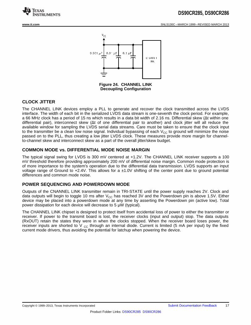
Bypassing capacitors are needed to reduce the impact of switching noise which could limit performance. For aconservative approach three parallel-connected decoupling capacitors (Multi-Layered Ceramic type in surfacemount form factor) between each VCC and the ground plane(s) are recommended. The three capacitor values are0.1 μF, 0.01μF and 0.001 μF. An example is shown in Figure 24. The designer should employ wide traces forpower and ground and ensure each capacitor has its own via to the ground plane. If board space is limiting thenumber of bypass capacitors, the PLL VCC should receive the most filtering/bypassing. Next would be the LVDSVCC pins and finally the logic VCC pins.
Figure 23. LVDS Serialized Link Termination
16 Submit Documentation Feedback Copyright © 1999–2013, Texas Instruments Incorporated
Product Folder Links: DS90CR285 DS90CR286
DS90CR285, DS90CR286
www.ti.com SNLS130C –MARCH 1999–REVISED MARCH 2013
Figure 24. CHANNEL LINKDecoupling Configuration
CLOCK JITTER
The CHANNEL LINK devices employ a PLL to generate and recover the clock transmitted across the LVDSinterface. The width of each bit in the serialized LVDS data stream is one-seventh the clock period. For example,a 66 MHz clock has a period of 15 ns which results in a data bit width of 2.16 ns. Differential skew (Δt within onedifferential pair), interconnect skew (Δt of one differential pair to another) and clock jitter will all reduce theavailable window for sampling the LVDS serial data streams. Care must be taken to ensure that the clock inputto the transmitter be a clean low noise signal. Individual bypassing of each VCC to ground will minimize the noisepassed on to the PLL, thus creating a low jitter LVDS clock. These measures provide more margin for channel-to-channel skew and interconnect skew as a part of the overall jitter/skew budget.
COMMON MODE vs. DIFFERENTIAL MODE NOISE MARGIN
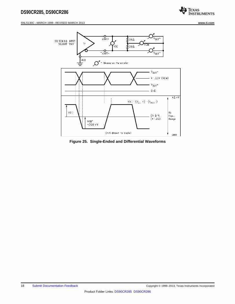
The typical signal swing for LVDS is 300 mV centered at +1.2V. The CHANNEL LINK receiver supports a 100mV threshold therefore providing approximately 200 mV of differential noise margin. Common mode protection isof more importance to the system's operation due to the differential data transmission. LVDS supports an inputvoltage range of Ground to +2.4V. This allows for a ±1.0V shifting of the center point due to ground potentialdifferences and common mode noise.
POWER SEQUENCING AND POWERDOWN MODE
Outputs of the CNANNEL LINK transmitter remain in TRI-STATE until the power supply reaches 2V. Clock anddata outputs will begin to toggle 10 ms after VCC has reached 3V and the Powerdown pin is above 1.5V. Eitherdevice may be placed into a powerdown mode at any time by asserting the Powerdown pin (active low). Totalpower dissipation for each device will decrease to 5 μW (typical).
The CHANNEL LINK chipset is designed to protect itself from accidental loss of power to either the transmitter orreceiver. If power to the transmit board is lost, the receiver clocks (input and output) stop. The data outputs(RxOUT) retain the states they were in when the clocks stopped. When the receiver board loses power, thereceiver inputs are shorted to V CC through an internal diode. Current is limited (5 mA per input) by the fixedcurrent mode drivers, thus avoiding the potential for latchup when powering the device.
Copyright © 1999–2013, Texas Instruments Incorporated Submit Documentation Feedback 17
Product Folder Links: DS90CR285 DS90CR286
DS90CR285, DS90CR286
SNLS130C –MARCH 1999–REVISED MARCH 2013 www.ti.com
Figure 25. Single-Ended and Differential Waveforms
18 Submit Documentation Feedback Copyright © 1999–2013, Texas Instruments Incorporated
Product Folder Links: DS90CR285 DS90CR286

DS90CR285, DS90CR286
www.ti.com SNLS130C –MARCH 1999–REVISED MARCH 2013
REVISION HISTORY
Changes from Revision B (March 2013) to Revision C Page
• Changed layout of National Data Sheet to TI format .......................................................................................................... 18
Copyright © 1999–2013, Texas Instruments Incorporated Submit Documentation Feedback 19
Product Folder Links: DS90CR285 DS90CR286
PACKAGE OPTION ADDENDUM
www.ti.com 1-Nov-2013
Addendum-Page 1
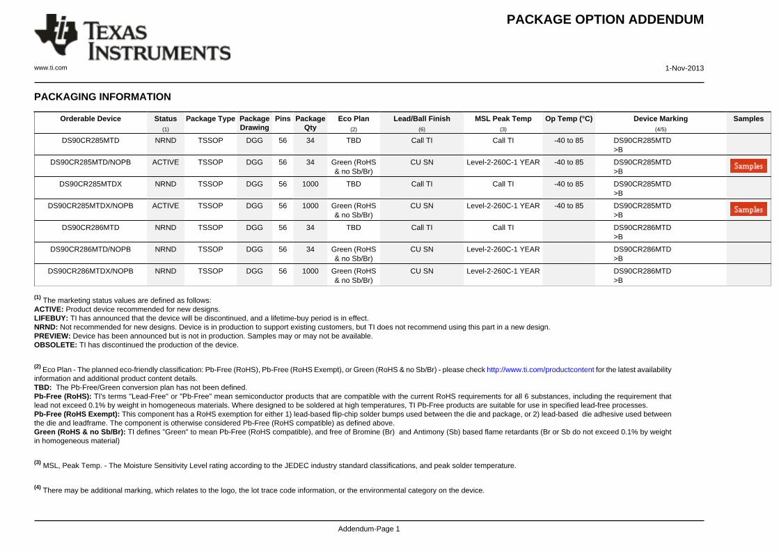
PACKAGING INFORMATION
Orderable Device Status(1)
Package Type PackageDrawing
Pins PackageQty
Eco Plan(2)
Lead/Ball Finish(6)
MSL Peak Temp(3)
Op Temp (°C) Device Marking(4/5)
Samples
DS90CR285MTD NRND TSSOP DGG 56 34 TBD Call TI Call TI -40 to 85 DS90CR285MTD>B
DS90CR285MTD/NOPB ACTIVE TSSOP DGG 56 34 Green (RoHS& no Sb/Br)
CU SN Level-2-260C-1 YEAR -40 to 85 DS90CR285MTD>B
DS90CR285MTDX NRND TSSOP DGG 56 1000 TBD Call TI Call TI -40 to 85 DS90CR285MTD>B
DS90CR285MTDX/NOPB ACTIVE TSSOP DGG 56 1000 Green (RoHS& no Sb/Br)
CU SN Level-2-260C-1 YEAR -40 to 85 DS90CR285MTD>B
DS90CR286MTD NRND TSSOP DGG 56 34 TBD Call TI Call TI DS90CR286MTD>B
DS90CR286MTD/NOPB NRND TSSOP DGG 56 34 Green (RoHS& no Sb/Br)
CU SN Level-2-260C-1 YEAR DS90CR286MTD>B
DS90CR286MTDX/NOPB NRND TSSOP DGG 56 1000 Green (RoHS& no Sb/Br)
CU SN Level-2-260C-1 YEAR DS90CR286MTD>B
(1) The marketing status values are defined as follows:ACTIVE: Product device recommended for new designs.LIFEBUY: TI has announced that the device will be discontinued, and a lifetime-buy period is in effect.NRND: Not recommended for new designs. Device is in production to support existing customers, but TI does not recommend using this part in a new design.PREVIEW: Device has been announced but is not in production. Samples may or may not be available.OBSOLETE: TI has discontinued the production of the device.
(2) Eco Plan - The planned eco-friendly classification: Pb-Free (RoHS), Pb-Free (RoHS Exempt), or Green (RoHS & no Sb/Br) - please check http://www.ti.com/productcontent for the latest availabilityinformation and additional product content details.TBD: The Pb-Free/Green conversion plan has not been defined.Pb-Free (RoHS): TI's terms "Lead-Free" or "Pb-Free" mean semiconductor products that are compatible with the current RoHS requirements for all 6 substances, including the requirement thatlead not exceed 0.1% by weight in homogeneous materials. Where designed to be soldered at high temperatures, TI Pb-Free products are suitable for use in specified lead-free processes.Pb-Free (RoHS Exempt): This component has a RoHS exemption for either 1) lead-based flip-chip solder bumps used between the die and package, or 2) lead-based die adhesive used betweenthe die and leadframe. The component is otherwise considered Pb-Free (RoHS compatible) as defined above.Green (RoHS & no Sb/Br): TI defines "Green" to mean Pb-Free (RoHS compatible), and free of Bromine (Br) and Antimony (Sb) based flame retardants (Br or Sb do not exceed 0.1% by weightin homogeneous material)
(3) MSL, Peak Temp. - The Moisture Sensitivity Level rating according to the JEDEC industry standard classifications, and peak solder temperature.
(4) There may be additional marking, which relates to the logo, the lot trace code information, or the environmental category on the device.

PACKAGE OPTION ADDENDUM
www.ti.com 1-Nov-2013
Addendum-Page 2
(5) Multiple Device Markings will be inside parentheses. Only one Device Marking contained in parentheses and separated by a "~" will appear on a device. If a line is indented then it is a continuationof the previous line and the two combined represent the entire Device Marking for that device.
(6) Lead/Ball Finish - Orderable Devices may have multiple material finish options. Finish options are separated by a vertical ruled line. Lead/Ball Finish values may wrap to two lines if the finishvalue exceeds the maximum column width.
Important Information and Disclaimer:The information provided on this page represents TI's knowledge and belief as of the date that it is provided. TI bases its knowledge and belief on informationprovided by third parties, and makes no representation or warranty as to the accuracy of such information. Efforts are underway to better integrate information from third parties. TI has taken andcontinues to take reasonable steps to provide representative and accurate information but may not have conducted destructive testing or chemical analysis on incoming materials and chemicals.TI and TI suppliers consider certain information to be proprietary, and thus CAS numbers and other limited information may not be available for release.
In no event shall TI's liability arising out of such information exceed the total purchase price of the TI part(s) at issue in this document sold by TI to Customer on an annual basis.
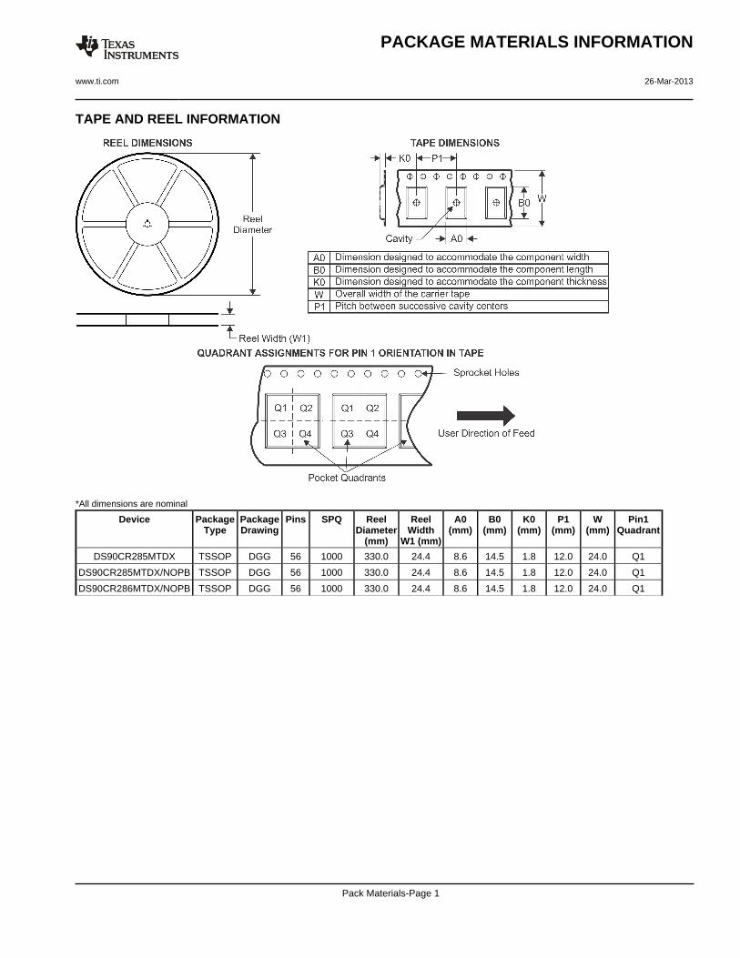
TAPE AND REEL INFORMATION
*All dimensions are nominal
Device PackageType
PackageDrawing
Pins SPQ ReelDiameter
(mm)
ReelWidth
W1 (mm)
A0(mm)
B0(mm)
K0(mm)
P1(mm)
W(mm)
Pin1Quadrant
DS90CR285MTDX TSSOP DGG 56 1000 330.0 24.4 8.6 14.5 1.8 12.0 24.0 Q1
DS90CR285MTDX/NOPB TSSOP DGG 56 1000 330.0 24.4 8.6 14.5 1.8 12.0 24.0 Q1
DS90CR286MTDX/NOPB TSSOP DGG 56 1000 330.0 24.4 8.6 14.5 1.8 12.0 24.0 Q1
PACKAGE MATERIALS INFORMATION
www.ti.com 26-Mar-2013
Pack Materials-Page 1

*All dimensions are nominal
Device Package Type Package Drawing Pins SPQ Length (mm) Width (mm) Height (mm)
DS90CR285MTDX TSSOP DGG 56 1000 367.0 367.0 45.0
DS90CR285MTDX/NOPB TSSOP DGG 56 1000 367.0 367.0 45.0
DS90CR286MTDX/NOPB TSSOP DGG 56 1000 367.0 367.0 45.0
PACKAGE MATERIALS INFORMATION
www.ti.com 26-Mar-2013
Pack Materials-Page 2

www.ti.com
PACKAGE OUTLINE
C
TYP8.37.9
1.2 MAX
54X 0.5
56X 0.270.17
2X13.5
(0.15) TYP
0 - 80.150.05
0.25GAGE PLANE
0.750.50
A
NOTE 3
14.113.9
B 6.26.0
4222167/A 07/2015
TSSOP - 1.2 mm max heightDGG0056ASMALL OUTLINE PACKAGE
NOTES: 1. All linear dimensions are in millimeters. Any dimensions in parenthesis are for reference only. Dimensioning and tolerancing per ASME Y14.5M. 2. This drawing is subject to change without notice. 3. This dimension does not include mold flash, protrusions, or gate burrs. Mold flash, protrusions, or gate burrs shall not exceed 0.15 mm per side.4. Reference JEDEC registration MO-153.
156
0.08 C A B
2928
PIN 1 IDAREA
SEATING PLANE
0.1 C
SEE DETAIL A
DETAIL ATYPICAL
SCALE 1.200

www.ti.com
EXAMPLE BOARD LAYOUT
(7.5)
0.05 MAXALL AROUND
0.05 MINALL AROUND
56X (1.5)
56X (0.3)
54X (0.5)
(R )TYP
0.05
4222167/A 07/2015
TSSOP - 1.2 mm max heightDGG0056ASMALL OUTLINE PACKAGE
SYMM
SYMM
LAND PATTERN EXAMPLESCALE:6X
1
28 29
56
NOTES: (continued) 5. Publication IPC-7351 may have alternate designs. 6. Solder mask tolerances between and around signal pads can vary based on board fabrication site.
METALSOLDER MASKOPENING
NON SOLDER MASKDEFINED
SOLDER MASK DETAILS
SOLDER MASKOPENING
METAL UNDERSOLDER MASK
SOLDER MASKDEFINED

www.ti.com
EXAMPLE STENCIL DESIGN
(7.5)
54X (0.5)
56X (0.3)
56X (1.5)
(R ) TYP0.05
4222167/A 07/2015
TSSOP - 1.2 mm max heightDGG0056ASMALL OUTLINE PACKAGE
NOTES: (continued) 7. Laser cutting apertures with trapezoidal walls and rounded corners may offer better paste release. IPC-7525 may have alternate design recommendations. 8. Board assembly site may have different recommendations for stencil design.
SYMM
SYMM
1
28 29
56
SOLDER PASTE EXAMPLEBASED ON 0.125 mm THICK STENCIL
SCALE:6X

IMPORTANT NOTICE
Texas Instruments Incorporated and its subsidiaries (TI) reserve the right to make corrections, enhancements, improvements and otherchanges to its semiconductor products and services per JESD46, latest issue, and to discontinue any product or service per JESD48, latestissue. Buyers should obtain the latest relevant information before placing orders and should verify that such information is current andcomplete. All semiconductor products (also referred to herein as “components”) are sold subject to TI’s terms and conditions of salesupplied at the time of order acknowledgment.TI warrants performance of its components to the specifications applicable at the time of sale, in accordance with the warranty in TI’s termsand conditions of sale of semiconductor products. Testing and other quality control techniques are used to the extent TI deems necessaryto support this warranty. Except where mandated by applicable law, testing of all parameters of each component is not necessarilyperformed.TI assumes no liability for applications assistance or the design of Buyers’ products. Buyers are responsible for their products andapplications using TI components. To minimize the risks associated with Buyers’ products and applications, Buyers should provideadequate design and operating safeguards.TI does not warrant or represent that any license, either express or implied, is granted under any patent right, copyright, mask work right, orother intellectual property right relating to any combination, machine, or process in which TI components or services are used. Informationpublished by TI regarding third-party products or services does not constitute a license to use such products or services or a warranty orendorsement thereof. Use of such information may require a license from a third party under the patents or other intellectual property of thethird party, or a license from TI under the patents or other intellectual property of TI.Reproduction of significant portions of TI information in TI data books or data sheets is permissible only if reproduction is without alterationand is accompanied by all associated warranties, conditions, limitations, and notices. TI is not responsible or liable for such altereddocumentation. Information of third parties may be subject to additional restrictions.Resale of TI components or services with statements different from or beyond the parameters stated by TI for that component or servicevoids all express and any implied warranties for the associated TI component or service and is an unfair and deceptive business practice.TI is not responsible or liable for any such statements.Buyer acknowledges and agrees that it is solely responsible for compliance with all legal, regulatory and safety-related requirementsconcerning its products, and any use of TI components in its applications, notwithstanding any applications-related information or supportthat may be provided by TI. Buyer represents and agrees that it has all the necessary expertise to create and implement safeguards whichanticipate dangerous consequences of failures, monitor failures and their consequences, lessen the likelihood of failures that might causeharm and take appropriate remedial actions. Buyer will fully indemnify TI and its representatives against any damages arising out of the useof any TI components in safety-critical applications.In some cases, TI components may be promoted specifically to facilitate safety-related applications. With such components, TI’s goal is tohelp enable customers to design and create their own end-product solutions that meet applicable functional safety standards andrequirements. Nonetheless, such components are subject to these terms.No TI components are authorized for use in FDA Class III (or similar life-critical medical equipment) unless authorized officers of the partieshave executed a special agreement specifically governing such use.Only those TI components which TI has specifically designated as military grade or “enhanced plastic” are designed and intended for use inmilitary/aerospace applications or environments. Buyer acknowledges and agrees that any military or aerospace use of TI componentswhich have not been so designated is solely at the Buyer's risk, and that Buyer is solely responsible for compliance with all legal andregulatory requirements in connection with such use.TI has specifically designated certain components as meeting ISO/TS16949 requirements, mainly for automotive use. In any case of use ofnon-designated products, TI will not be responsible for any failure to meet ISO/TS16949.
Products ApplicationsAudio www.ti.com/audio Automotive and Transportation www.ti.com/automotiveAmplifiers amplifier.ti.com Communications and Telecom www.ti.com/communicationsData Converters dataconverter.ti.com Computers and Peripherals www.ti.com/computersDLP® Products www.dlp.com Consumer Electronics www.ti.com/consumer-appsDSP dsp.ti.com Energy and Lighting www.ti.com/energyClocks and Timers www.ti.com/clocks Industrial www.ti.com/industrialInterface interface.ti.com Medical www.ti.com/medicalLogic logic.ti.com Security www.ti.com/securityPower Mgmt power.ti.com Space, Avionics and Defense www.ti.com/space-avionics-defenseMicrocontrollers microcontroller.ti.com Video and Imaging www.ti.com/videoRFID www.ti-rfid.comOMAP Applications Processors www.ti.com/omap TI E2E Community e2e.ti.comWireless Connectivity www.ti.com/wirelessconnectivity
Mailing Address: Texas Instruments, Post Office Box 655303, Dallas, Texas 75265Copyright © 2016, Texas Instruments Incorporated