![PEP I1 16-Channel Corrector Controller Using BITBUS'/67531/metadc689960/m2/1/high_re… · BITBUS, a subset of SDLC [2]. The individual packet length is limited to 43 bytes due to](https://static.fdocuments.net/doc/165x107/5ebb7a858772db18c74d18fa/pep-i1-16-channel-corrector-controller-using-bitbus-67531metadc689960m21highre.jpg)
SN74LVC861A 10-BITBUS TRANSCEIVER WITH 3-STATEOUTPUTS · This 10-bitbus transceiver is designed for...
16
www.ti.com FEATURES DB, DGV, DW, NS, OR PW PACKAGE (TOP VIEW) 1 2 3 4 5 6 7 8 9 10 11 12 24 23 22 21 20 19 18 17 16 15 14 13 OEBA A1 A2 A3 A4 A5 A6 A7 A8 A9 A10 GND V CC B1 B2 B3 B4 B5 B6 B7 B8 B9 B10 OEAB DESCRIPTION/ORDERING INFORMATION SN74LVC861A 10-BIT BUS TRANSCEIVER WITH 3-STATE OUTPUTS SCAS309I – MARCH 1993 – REVISED FEBRUARY 2005 • Operates From 1.65 V to 3.6 V • Inputs Accept Voltages to 5.5 V • Max t pd of 6.4 ns at 3.3 V • Typical V OLP (Output Ground Bounce) <0.8 V at V CC = 3.3 V, T A = 25°C • Typical V OHV (Output V OH Undershoot) >2 V at V CC = 3.3 V, T A = 25°C • Supports Mixed-Mode Signal Operation on All Ports (5-V Input/Output Voltage With 3.3-V V CC ) • I off Supports Partial-Power-Down Mode Operation • Latch-Up Performance Exceeds 250 mA Per JESD 17 • ESD Protection Exceeds JESD 22 – 2000-V Human-Body Model (A114-A) – 200-V Machine Model (A115-A) – 1000-V Charged-Device Model (C101) This 10-bit bus transceiver is designed for 1.65-V to 3.6-V V CC operation. The SN74LVC861A is designed for asynchronous communication between data buses. The control-function implementation allows for maximum flexibility in timing. This device allows data transmission from the A bus to the B bus or from the B bus to the A bus, depending on the logic levels at the output-enable (OEAB and OEBA) inputs. Inputs can be driven from either 3.3-V or 5-V devices. This feature allows the use of this device as a translator in a mixed 3.3-V/5-V system environment. To ensure the high-impedance state during power up or power down, OE should be tied to V CC through a pullup resistor; the minimum value of the resistor is determined by the current-sinking capability of the driver. This device is fully specified for partial-power-down applications using I off . The I off circuitry disables the outputs, preventing damaging current backflow through the device when it is powered down. ORDERING INFORMATION T A PACKAGE (1) ORDERABLE PART NUMBER TOP-SIDE MARKING Tube of 25 SN74LVC861ADW SOIC – DW LVC861A Reel of 2000 SN74LVC861ADWR SOP – NS Reel of 2000 SN74LVC861ANSR LVC861A SSOP – DB Reel of 2000 SN74LVC861ADBR LC861A –40°C to 85°C Tube of 60 SN74LVC861APW TSSOP – PW Reel of 2000 SN74LVC861APWR LC861A Reel of 250 SN74LVC861APWT TVSOP – DGV Reel of 2000 SN74LVC861ADGVR LC861A (1) Package drawings, standard packing quantities, thermal data, symbolization, and PCB design guidelines are available at www.ti.com/sc/package. Please be aware that an important notice concerning availability, standard warranty, and use in critical applications of Texas Instruments semiconductor products and disclaimers thereto appears at the end of this data sheet. PRODUCTION DATA information is current as of publication date. Copyright © 1993–2005, Texas Instruments Incorporated Products conform to specifications per the terms of the Texas Instruments standard warranty. Production processing does not necessarily include testing of all parameters.
Transcript of SN74LVC861A 10-BITBUS TRANSCEIVER WITH 3-STATEOUTPUTS · This 10-bitbus transceiver is designed for...

www.ti.com
FEATURESDB, DGV, DW, NS, OR PW PACKAGE
(TOP VIEW)
1
2
3
4
5
6
7
8
9
10
11
12
24
23
22
21
20
19
18
17
16
15
14
13
OEBAA1A2A3A4A5A6A7A8A9
A10GND
VCC
B1B2B3B4B5B6B7B8B9B10OEAB
DESCRIPTION/ORDERING INFORMATION
SN74LVC861A10-BIT BUS TRANSCEIVER
WITH 3-STATE OUTPUTSSCAS309I–MARCH 1993–REVISED FEBRUARY 2005
• Operates From 1.65 V to 3.6 V• Inputs Accept Voltages to 5.5 V• Max tpd of 6.4 ns at 3.3 V• Typical VOLP (Output Ground Bounce)
<0.8 V at VCC = 3.3 V, TA = 25°C• Typical VOHV (Output VOH Undershoot)
>2 V at VCC = 3.3 V, TA = 25°C• Supports Mixed-Mode Signal Operation on
All Ports (5-V Input/Output Voltage With3.3-V VCC)
• Ioff Supports Partial-Power-Down ModeOperation
• Latch-Up Performance Exceeds 250 mA PerJESD 17
• ESD Protection Exceeds JESD 22– 2000-V Human-Body Model (A114-A)– 200-V Machine Model (A115-A)– 1000-V Charged-Device Model (C101)
This 10-bit bus transceiver is designed for 1.65-V to 3.6-V VCC operation.
The SN74LVC861A is designed for asynchronous communication between data buses. The control-functionimplementation allows for maximum flexibility in timing.
This device allows data transmission from the A bus to the B bus or from the B bus to the A bus, depending onthe logic levels at the output-enable (OEAB and OEBA) inputs.
Inputs can be driven from either 3.3-V or 5-V devices. This feature allows the use of this device as a translator ina mixed 3.3-V/5-V system environment.
To ensure the high-impedance state during power up or power down, OE should be tied to VCC through a pullupresistor; the minimum value of the resistor is determined by the current-sinking capability of the driver.
This device is fully specified for partial-power-down applications using Ioff. The Ioff circuitry disables the outputs,preventing damaging current backflow through the device when it is powered down.
ORDERING INFORMATION
TA PACKAGE (1) ORDERABLE PART NUMBER TOP-SIDE MARKING
Tube of 25 SN74LVC861ADWSOIC – DW LVC861A
Reel of 2000 SN74LVC861ADWR
SOP – NS Reel of 2000 SN74LVC861ANSR LVC861A
SSOP – DB Reel of 2000 SN74LVC861ADBR LC861A–40°C to 85°C
Tube of 60 SN74LVC861APW
TSSOP – PW Reel of 2000 SN74LVC861APWR LC861A
Reel of 250 SN74LVC861APWT
TVSOP – DGV Reel of 2000 SN74LVC861ADGVR LC861A
(1) Package drawings, standard packing quantities, thermal data, symbolization, and PCB design guidelines are available atwww.ti.com/sc/package.
Please be aware that an important notice concerning availability, standard warranty, and use in critical applications of TexasInstruments semiconductor products and disclaimers thereto appears at the end of this data sheet.
PRODUCTION DATA information is current as of publication date. Copyright © 1993–2005, Texas Instruments IncorporatedProducts conform to specifications per the terms of the TexasInstruments standard warranty. Production processing does notnecessarily include testing of all parameters.

www.ti.com
A1 B1
OEBA
OEAB
To Nine Other Channels
1
13
2 23
SN74LVC861A10-BIT BUS TRANSCEIVERWITH 3-STATE OUTPUTSSCAS309I–MARCH 1993–REVISED FEBRUARY 2005
FUNCTION TABLE
INPUTSOPERATION
OEAB OEBA
L H A data to B bus
H L B data to A bus
H H Isolation
Latch A and BL L (A = B)
LOGIC DIAGRAM (POSITIVE LOGIC)
2
www.ti.com
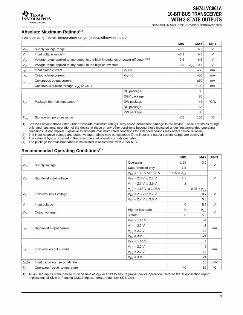
Absolute Maximum Ratings (1)
Recommended Operating Conditions (1)
SN74LVC861A10-BIT BUS TRANSCEIVER
WITH 3-STATE OUTPUTSSCAS309I–MARCH 1993–REVISED FEBRUARY 2005
over operating free-air temperature range (unless otherwise noted)
MIN MAX UNIT
VCC Supply voltage range –0.5 6.5 V
VI Input voltage range (2) –0.5 6.5 V
VO Voltage range applied to any output in the high-impedance or power-off state (2) (3) –0.5 6.5 V
VO Voltage range applied to any output in the high or low state –0.5 VCC + 0.5 V
IIK Input clamp current VI < 0 –50 mA
IOK Output clamp current VO < 0 –50 mA
IO Continuous output current ±50 mA
Continuous current through VCC or GND ±100 mA
DB package 63
DGV package 86
θJA Package thermal impedance (4) DW package 46 °C/W
NS package 65
PW package 88
Tstg Storage temperature range –65 150 °C
(1) Stresses beyond those listed under "absolute maximum ratings" may cause permanent damage to the device. These are stress ratingsonly, and functional operation of the device at these or any other conditions beyond those indicated under "recommended operatingconditions" is not implied. Exposure to absolute-maximum-rated conditions for extended periods may affect device reliability.
(2) The input negative-voltage and output voltage ratings may be exceeded if the input and output current ratings are observed.(3) The value of VCC is provided in the recommended operating conditions table.(4) The package thermal impedance is calculated in accordance with JESD 51-7.
MIN MAX UNIT
Operating 1.65 3.6VCC Supply voltage V
Data retention only 1.5
VCC = 1.65 V to 1.95 V 0.65 × VCC
VIH High-level input voltage VCC = 2.3 V to 2.7 V 1.7 V
VCC = 2.7 V to 3.6 V 2
VCC = 1.65 V to 1.95 V 0.35 × VCC
VIL Low-level input voltage VCC = 2.3 V to 2.7 V 0.7 V
VCC = 2.7 V to 3.6 V 0.8
VI Input voltage 0 5.5 V
High or low state 0 VCCVO Output voltage V
3-state 0 5.5
VCC = 1.65 V –4
VCC = 2.3 V –8IOH High-level output current mA
VCC = 2.7 V –12
VCC = 3 V –24
VCC = 1.65 V 4
VCC = 2.3 V 8IOL Low-level output current mA
VCC = 2.7 V 12
VCC = 3 V 24
∆t/∆v Input transition rise or fall rate 10 ns/V
TA Operating free-air temperature –40 85 °C
(1) All unused inputs of the device must be held at VCC or GND to ensure proper device operation. Refer to the TI application report,Implications of Slow or Floating CMOS Inputs, literature number SCBA004.
3
www.ti.com
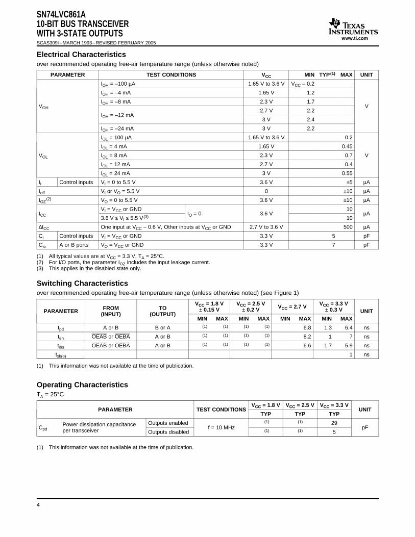
Electrical Characteristics
Switching Characteristics
Operating Characteristics
SN74LVC861A10-BIT BUS TRANSCEIVERWITH 3-STATE OUTPUTSSCAS309I–MARCH 1993–REVISED FEBRUARY 2005
over recommended operating free-air temperature range (unless otherwise noted)
PARAMETER TEST CONDITIONS VCC MIN TYP (1) MAX UNIT
IOH = –100 µA 1.65 V to 3.6 V VCC – 0.2
IOH = –4 mA 1.65 V 1.2
IOH = –8 mA 2.3 V 1.7VOH V
2.7 V 2.2IOH = –12 mA
3 V 2.4
IOH = –24 mA 3 V 2.2
IOL = 100 µA 1.65 V to 3.6 V 0.2
IOL = 4 mA 1.65 V 0.45
VOL IOL = 8 mA 2.3 V 0.7 V
IOL = 12 mA 2.7 V 0.4
IOL = 24 mA 3 V 0.55
II Control inputs VI = 0 to 5.5 V 3.6 V ±5 µA
Ioff VI or VO = 5.5 V 0 ±10 µA
IOZ(2) VO = 0 to 5.5 V 3.6 V ±10 µA
VI = VCC or GND 10ICC IO = 0 3.6 V µA
3.6 V ≤ VI ≤ 5.5 V (3) 10
∆ICC One input at VCC – 0.6 V, Other inputs at VCC or GND 2.7 V to 3.6 V 500 µA
Ci Control inputs VI = VCC or GND 3.3 V 5 pF
Cio A or B ports VO = VCC or GND 3.3 V 7 pF
(1) All typical values are at VCC = 3.3 V, TA = 25°C.(2) For I/O ports, the parameter IOZ includes the input leakage current.(3) This applies in the disabled state only.
over recommended operating free-air temperature range (unless otherwise noted) (see Figure 1)
VCC = 1.8 V VCC = 2.5 V VCC = 3.3 VVCC = 2.7 VFROM TO ± 0.15 V ± 0.2 V ± 0.3 VPARAMETER UNIT(INPUT) (OUTPUT)MIN MAX MIN MAX MIN MAX MIN MAX
tpd A or B B or A (1) (1) (1) (1) 6.8 1.3 6.4 ns
ten OEAB or OEBA A or B (1) (1) (1) (1) 8.2 1 7 ns
tdis OEAB or OEBA A or B (1) (1) (1) (1) 6.6 1.7 5.9 ns
tsk(o) 1 ns
(1) This information was not available at the time of publication.
TA = 25°C
VCC = 1.8 V VCC = 2.5 V VCC = 3.3 VPARAMETER TEST CONDITIONS UNIT
TYP TYP TYP
Outputs enabled (1) (1) 29Power dissipation capacitanceCpd f = 10 MHz pFper transceiver Outputs disabled (1) (1) 5
(1) This information was not available at the time of publication.
4
www.ti.com
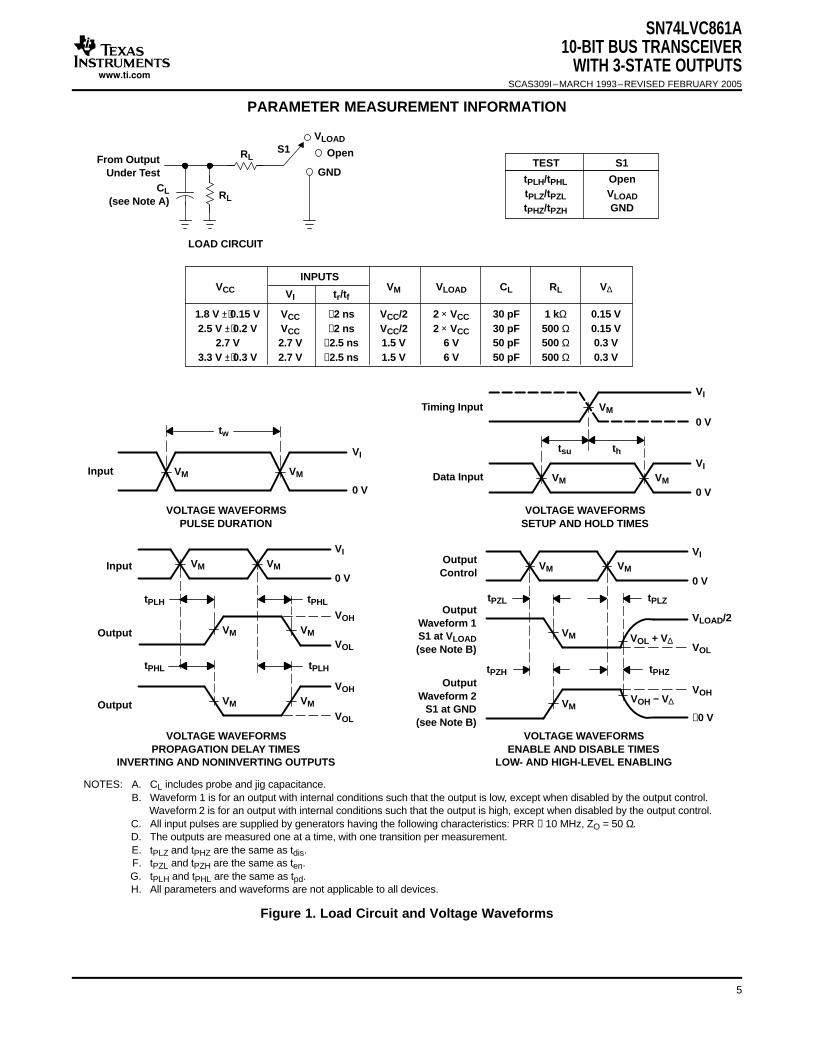
PARAMETER MEASUREMENT INFORMATION
VM
thtsu
From OutputUnder Test
CL(see Note A)
LOAD CIRCUIT
S1VLOAD
Open
GND
RL
RL
Data Input
Timing InputVI
0 V
VI
0 V0 V
tw
Input
VOLTAGE WAVEFORMSSETUP AND HOLD TIMES
VOLTAGE WAVEFORMSPROPAGATION DELAY TIMES
INVERTING AND NONINVERTING OUTPUTS
VOLTAGE WAVEFORMSPULSE DURATION
tPLH
tPHL
tPHL
tPLH
VOH
VOH
VOL
VOL
VI
0 VInput
OutputWaveform 1S1 at VLOAD(see Note B)
OutputWaveform 2
S1 at GND(see Note B)
VOL
VOH
tPZL
tPZH
tPLZ
tPHZ
VLOAD/2
0 V
VOL + V∆
VOH − V∆
≈0 V
VI
VOLTAGE WAVEFORMSENABLE AND DISABLE TIMES
LOW- AND HIGH-LEVEL ENABLING
Output
Output
tPLH/tPHLtPLZ/tPZLtPHZ/tPZH
OpenVLOADGND
TEST S1
NOTES: A. CL includes probe and jig capacitance.B. Waveform 1 is for an output with internal conditions such that the output is low, except when disabled by the output control.
Waveform 2 is for an output with internal conditions such that the output is high, except when disabled by the output control.C. All input pulses are supplied by generators having the following characteristics: PRR ≤ 10 MHz, ZO = 50 Ω.D. The outputs are measured one at a time, with one transition per measurement.E. tPLZ and tPHZ are the same as tdis.F. tPZL and tPZH are the same as ten.G. tPLH and tPHL are the same as tpd.H. All parameters and waveforms are not applicable to all devices.
OutputControl
VM VM
VM VM
VM VM
VM
VM VM
VM
VM
VM
VI
VM
VM
1.8 V ± 0.15 V2.5 V ± 0.2 V
2.7 V3.3 V ± 0.3 V
1 kΩ500 Ω500 Ω500 Ω
VCC RL
2 × VCC2 × VCC
6 V6 V
VLOAD CL
30 pF30 pF50 pF50 pF
0.15 V0.15 V0.3 V0.3 V
V∆
VCCVCC2.7 V2.7 V
VI
VCC/2VCC/21.5 V1.5 V
VMtr/tf
≤2 ns≤2 ns
≤2.5 ns≤2.5 ns
INPUTS
SN74LVC861A10-BIT BUS TRANSCEIVER
WITH 3-STATE OUTPUTSSCAS309I–MARCH 1993–REVISED FEBRUARY 2005
Figure 1. Load Circuit and Voltage Waveforms
5
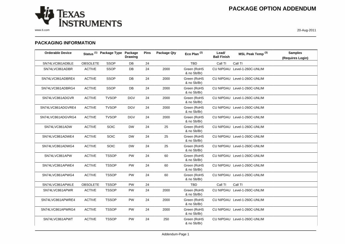
PACKAGE OPTION ADDENDUM
www.ti.com 20-Aug-2011
Addendum-Page 1
PACKAGING INFORMATION
Orderable Device Status (1) Package Type PackageDrawing
Pins Package Qty Eco Plan (2) Lead/Ball Finish
MSL Peak Temp (3) Samples
(Requires Login)
SN74LVC861ADBLE OBSOLETE SSOP DB 24 TBD Call TI Call TI
SN74LVC861ADBR ACTIVE SSOP DB 24 2000 Green (RoHS& no Sb/Br)
CU NIPDAU Level-1-260C-UNLIM
SN74LVC861ADBRE4 ACTIVE SSOP DB 24 2000 Green (RoHS& no Sb/Br)
CU NIPDAU Level-1-260C-UNLIM
SN74LVC861ADBRG4 ACTIVE SSOP DB 24 2000 Green (RoHS& no Sb/Br)
CU NIPDAU Level-1-260C-UNLIM
SN74LVC861ADGVR ACTIVE TVSOP DGV 24 2000 Green (RoHS& no Sb/Br)
CU NIPDAU Level-1-260C-UNLIM
SN74LVC861ADGVRE4 ACTIVE TVSOP DGV 24 2000 Green (RoHS& no Sb/Br)
CU NIPDAU Level-1-260C-UNLIM
SN74LVC861ADGVRG4 ACTIVE TVSOP DGV 24 2000 Green (RoHS& no Sb/Br)
CU NIPDAU Level-1-260C-UNLIM
SN74LVC861ADW ACTIVE SOIC DW 24 25 Green (RoHS& no Sb/Br)
CU NIPDAU Level-1-260C-UNLIM
SN74LVC861ADWE4 ACTIVE SOIC DW 24 25 Green (RoHS& no Sb/Br)
CU NIPDAU Level-1-260C-UNLIM
SN74LVC861ADWG4 ACTIVE SOIC DW 24 25 Green (RoHS& no Sb/Br)
CU NIPDAU Level-1-260C-UNLIM
SN74LVC861APW ACTIVE TSSOP PW 24 60 Green (RoHS& no Sb/Br)
CU NIPDAU Level-1-260C-UNLIM
SN74LVC861APWE4 ACTIVE TSSOP PW 24 60 Green (RoHS& no Sb/Br)
CU NIPDAU Level-1-260C-UNLIM
SN74LVC861APWG4 ACTIVE TSSOP PW 24 60 Green (RoHS& no Sb/Br)
CU NIPDAU Level-1-260C-UNLIM
SN74LVC861APWLE OBSOLETE TSSOP PW 24 TBD Call TI Call TI
SN74LVC861APWR ACTIVE TSSOP PW 24 2000 Green (RoHS& no Sb/Br)
CU NIPDAU Level-1-260C-UNLIM
SN74LVC861APWRE4 ACTIVE TSSOP PW 24 2000 Green (RoHS& no Sb/Br)
CU NIPDAU Level-1-260C-UNLIM
SN74LVC861APWRG4 ACTIVE TSSOP PW 24 2000 Green (RoHS& no Sb/Br)
CU NIPDAU Level-1-260C-UNLIM
SN74LVC861APWT ACTIVE TSSOP PW 24 250 Green (RoHS& no Sb/Br)
CU NIPDAU Level-1-260C-UNLIM

PACKAGE OPTION ADDENDUM
www.ti.com 20-Aug-2011
Addendum-Page 2
Orderable Device Status (1) Package Type PackageDrawing
Pins Package Qty Eco Plan (2) Lead/Ball Finish
MSL Peak Temp (3) Samples
(Requires Login)
SN74LVC861APWTE4 ACTIVE TSSOP PW 24 250 Green (RoHS& no Sb/Br)
CU NIPDAU Level-1-260C-UNLIM
SN74LVC861APWTG4 ACTIVE TSSOP PW 24 250 Green (RoHS& no Sb/Br)
CU NIPDAU Level-1-260C-UNLIM
(1) The marketing status values are defined as follows:ACTIVE: Product device recommended for new designs.LIFEBUY: TI has announced that the device will be discontinued, and a lifetime-buy period is in effect.NRND: Not recommended for new designs. Device is in production to support existing customers, but TI does not recommend using this part in a new design.PREVIEW: Device has been announced but is not in production. Samples may or may not be available.OBSOLETE: TI has discontinued the production of the device.
(2) Eco Plan - The planned eco-friendly classification: Pb-Free (RoHS), Pb-Free (RoHS Exempt), or Green (RoHS & no Sb/Br) - please check http://www.ti.com/productcontent for the latest availabilityinformation and additional product content details.TBD: The Pb-Free/Green conversion plan has not been defined.Pb-Free (RoHS): TI's terms "Lead-Free" or "Pb-Free" mean semiconductor products that are compatible with the current RoHS requirements for all 6 substances, including the requirement thatlead not exceed 0.1% by weight in homogeneous materials. Where designed to be soldered at high temperatures, TI Pb-Free products are suitable for use in specified lead-free processes.Pb-Free (RoHS Exempt): This component has a RoHS exemption for either 1) lead-based flip-chip solder bumps used between the die and package, or 2) lead-based die adhesive used betweenthe die and leadframe. The component is otherwise considered Pb-Free (RoHS compatible) as defined above.Green (RoHS & no Sb/Br): TI defines "Green" to mean Pb-Free (RoHS compatible), and free of Bromine (Br) and Antimony (Sb) based flame retardants (Br or Sb do not exceed 0.1% by weightin homogeneous material)
(3) MSL, Peak Temp. -- The Moisture Sensitivity Level rating according to the JEDEC industry standard classifications, and peak solder temperature.
Important Information and Disclaimer:The information provided on this page represents TI's knowledge and belief as of the date that it is provided. TI bases its knowledge and belief on informationprovided by third parties, and makes no representation or warranty as to the accuracy of such information. Efforts are underway to better integrate information from third parties. TI has taken andcontinues to take reasonable steps to provide representative and accurate information but may not have conducted destructive testing or chemical analysis on incoming materials and chemicals.TI and TI suppliers consider certain information to be proprietary, and thus CAS numbers and other limited information may not be available for release.
In no event shall TI's liability arising out of such information exceed the total purchase price of the TI part(s) at issue in this document sold by TI to Customer on an annual basis.
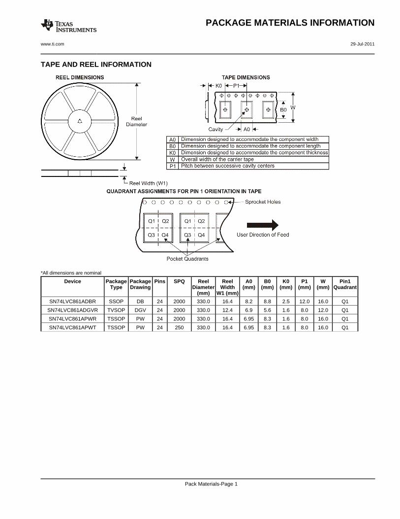
TAPE AND REEL INFORMATION
*All dimensions are nominal
Device PackageType
PackageDrawing
Pins SPQ ReelDiameter
(mm)
ReelWidth
W1 (mm)
A0(mm)
B0(mm)
K0(mm)
P1(mm)
W(mm)
Pin1Quadrant
SN74LVC861ADBR SSOP DB 24 2000 330.0 16.4 8.2 8.8 2.5 12.0 16.0 Q1
SN74LVC861ADGVR TVSOP DGV 24 2000 330.0 12.4 6.9 5.6 1.6 8.0 12.0 Q1
SN74LVC861APWR TSSOP PW 24 2000 330.0 16.4 6.95 8.3 1.6 8.0 16.0 Q1
SN74LVC861APWT TSSOP PW 24 250 330.0 16.4 6.95 8.3 1.6 8.0 16.0 Q1
PACKAGE MATERIALS INFORMATION
www.ti.com 29-Jul-2011
Pack Materials-Page 1

*All dimensions are nominal
Device Package Type Package Drawing Pins SPQ Length (mm) Width (mm) Height (mm)
SN74LVC861ADBR SSOP DB 24 2000 346.0 346.0 33.0
SN74LVC861ADGVR TVSOP DGV 24 2000 346.0 346.0 29.0
SN74LVC861APWR TSSOP PW 24 2000 346.0 346.0 33.0
SN74LVC861APWT TSSOP PW 24 250 346.0 346.0 33.0
PACKAGE MATERIALS INFORMATION
www.ti.com 29-Jul-2011
Pack Materials-Page 2
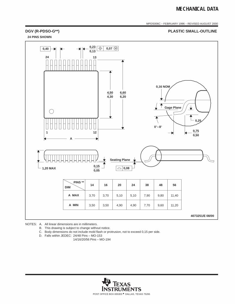
MECHANICAL DATA
MPDS006C – FEBRUARY 1996 – REVISED AUGUST 2000
POST OFFICE BOX 655303 • DALLAS, TEXAS 75265
DGV (R-PDSO-G**) PLASTIC SMALL-OUTLINE 24 PINS SHOWN
14
3,70
3,50 4,90
5,10
20DIM
PINS **
4073251/E 08/00
1,20 MAX
Seating Plane
0,050,15
0,25
0,500,75
0,230,13
1 12
24 13
4,304,50
0,16 NOM
Gage Plane
A
7,90
7,70
382416
4,90
5,103,70
3,50
A MAX
A MIN
6,606,20
11,20
11,40
56
9,60
9,80
48
0,08
M0,070,40
0°–8°
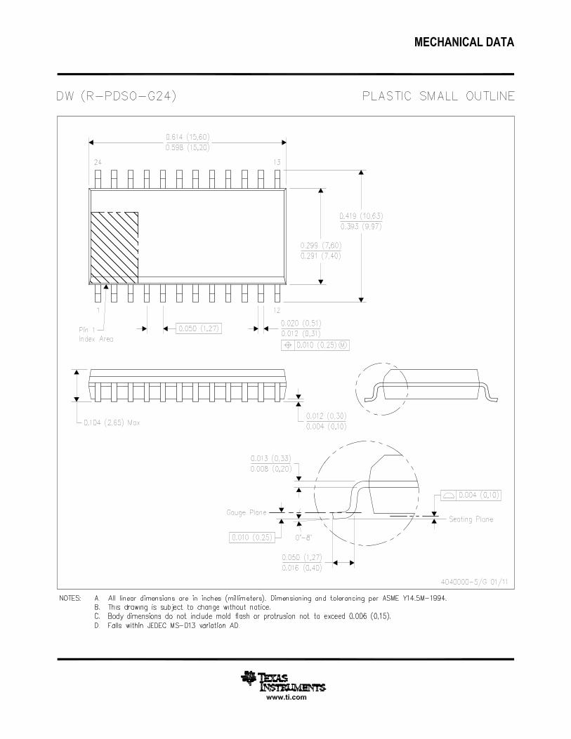
NOTES: A. All linear dimensions are in millimeters.B. This drawing is subject to change without notice.C. Body dimensions do not include mold flash or protrusion, not to exceed 0,15 per side.D. Falls within JEDEC: 24/48 Pins – MO-153
14/16/20/56 Pins – MO-194


MECHANICAL DATA
MSSO002E – JANUARY 1995 – REVISED DECEMBER 2001
POST OFFICE BOX 655303 • DALLAS, TEXAS 75265
DB (R-PDSO-G**) PLASTIC SMALL-OUTLINE
4040065 /E 12/01
28 PINS SHOWN
Gage Plane
8,207,40
0,550,95
0,25
38
12,90
12,30
28
10,50
24
8,50
Seating Plane
9,907,90
30
10,50
9,90
0,38
5,605,00
15
0,22
14
A
28
1
2016
6,506,50
14
0,05 MIN
5,905,90
DIM
A MAX
A MIN
PINS **
2,00 MAX
6,90
7,50
0,65 M0,15
0°–8°
0,10
0,090,25
NOTES: A. All linear dimensions are in millimeters.B. This drawing is subject to change without notice.C. Body dimensions do not include mold flash or protrusion not to exceed 0,15.D. Falls within JEDEC MO-150
IMPORTANT NOTICE
Texas Instruments Incorporated and its subsidiaries (TI) reserve the right to make corrections, modifications, enhancements, improvements,and other changes to its products and services at any time and to discontinue any product or service without notice. Customers shouldobtain the latest relevant information before placing orders and should verify that such information is current and complete. All products aresold subject to TI’s terms and conditions of sale supplied at the time of order acknowledgment.
TI warrants performance of its hardware products to the specifications applicable at the time of sale in accordance with TI’s standardwarranty. Testing and other quality control techniques are used to the extent TI deems necessary to support this warranty. Except wheremandated by government requirements, testing of all parameters of each product is not necessarily performed.
TI assumes no liability for applications assistance or customer product design. Customers are responsible for their products andapplications using TI components. To minimize the risks associated with customer products and applications, customers should provideadequate design and operating safeguards.
TI does not warrant or represent that any license, either express or implied, is granted under any TI patent right, copyright, mask work right,or other TI intellectual property right relating to any combination, machine, or process in which TI products or services are used. Informationpublished by TI regarding third-party products or services does not constitute a license from TI to use such products or services or awarranty or endorsement thereof. Use of such information may require a license from a third party under the patents or other intellectualproperty of the third party, or a license from TI under the patents or other intellectual property of TI.
Reproduction of TI information in TI data books or data sheets is permissible only if reproduction is without alteration and is accompaniedby all associated warranties, conditions, limitations, and notices. Reproduction of this information with alteration is an unfair and deceptivebusiness practice. TI is not responsible or liable for such altered documentation. Information of third parties may be subject to additionalrestrictions.
Resale of TI products or services with statements different from or beyond the parameters stated by TI for that product or service voids allexpress and any implied warranties for the associated TI product or service and is an unfair and deceptive business practice. TI is notresponsible or liable for any such statements.
TI products are not authorized for use in safety-critical applications (such as life support) where a failure of the TI product would reasonablybe expected to cause severe personal injury or death, unless officers of the parties have executed an agreement specifically governingsuch use. Buyers represent that they have all necessary expertise in the safety and regulatory ramifications of their applications, andacknowledge and agree that they are solely responsible for all legal, regulatory and safety-related requirements concerning their productsand any use of TI products in such safety-critical applications, notwithstanding any applications-related information or support that may beprovided by TI. Further, Buyers must fully indemnify TI and its representatives against any damages arising out of the use of TI products insuch safety-critical applications.
TI products are neither designed nor intended for use in military/aerospace applications or environments unless the TI products arespecifically designated by TI as military-grade or "enhanced plastic." Only products designated by TI as military-grade meet militaryspecifications. Buyers acknowledge and agree that any such use of TI products which TI has not designated as military-grade is solely atthe Buyer's risk, and that they are solely responsible for compliance with all legal and regulatory requirements in connection with such use.
TI products are neither designed nor intended for use in automotive applications or environments unless the specific TI products aredesignated by TI as compliant with ISO/TS 16949 requirements. Buyers acknowledge and agree that, if they use any non-designatedproducts in automotive applications, TI will not be responsible for any failure to meet such requirements.
Following are URLs where you can obtain information on other Texas Instruments products and application solutions:
Products Applications
Audio www.ti.com/audio Communications and Telecom www.ti.com/communications
Amplifiers amplifier.ti.com Computers and Peripherals www.ti.com/computers
Data Converters dataconverter.ti.com Consumer Electronics www.ti.com/consumer-apps
DLP® Products www.dlp.com Energy and Lighting www.ti.com/energy
DSP dsp.ti.com Industrial www.ti.com/industrial
Clocks and Timers www.ti.com/clocks Medical www.ti.com/medical
Interface interface.ti.com Security www.ti.com/security
Logic logic.ti.com Space, Avionics and Defense www.ti.com/space-avionics-defense
Power Mgmt power.ti.com Transportation and Automotive www.ti.com/automotive
Microcontrollers microcontroller.ti.com Video and Imaging www.ti.com/video
RFID www.ti-rfid.com
OMAP Mobile Processors www.ti.com/omap
Wireless Connctivity www.ti.com/wirelessconnectivity
TI E2E Community Home Page e2e.ti.com
Mailing Address: Texas Instruments, Post Office Box 655303, Dallas, Texas 75265Copyright © 2011, Texas Instruments Incorporated