
SmartLEWISTM TRX TDA5340 Evaluation Board and Explorer ...
52
Wireless Control SmartLEWIS TM TRX User Guide Rev1.0, 30/03/2012 TDA5340 Evaluation Board and Explorer Software Tooling
Transcript of SmartLEWISTM TRX TDA5340 Evaluation Board and Explorer ...

Wireless Control
SmartLEWISTM
TRX
User Guide
Rev1.0, 30/03/2012
TDA5340 Evaluation Board and Explorer Software Tooling

Edition 30/03/2012
Published by Infineon Technologies AG 81726 Munich, Germany
© 2012 Infineon Technologies AG All Rights Reserved.
LEGAL DISCLAIMER
THE INFORMATION GIVEN IN THIS APPLICATION NOTE IS GIVEN AS A HINT FOR THE IMPLEMENTATION OF THE INFINEON TECHNOLOGIES COMPONENT ONLY AND SHALL NOT BE REGARDED AS ANY DESCRIPTION OR WARRANTY OF A CERTAIN FUNCTIONALITY, CONDITION OR QUALITY OF THE INFINEON TECHNOLOGIES COMPONENT. THE RECIPIENT OF THIS APPLICATION NOTE MUST VERIFY ANY FUNCTION DESCRIBED HEREIN IN THE REAL APPLICATION. INFINEON TECHNOLOGIES HEREBY DISCLAIMS ANY AND ALL WARRANTIES AND LIABILITIES OF ANY KIND (INCLUDING WITHOUT LIMITATION WARRANTIES OF NON-INFRINGEMENT OF INTELLECTUAL PROPERTY RIGHTS OF ANY THIRD PARTY) WITH RESPECT TO ANY AND ALL INFORMATION GIVEN IN THIS APPLICATION NOTE.
Information
For further information on technology, delivery terms and conditions and prices, please contact the nearest Infineon Technologies Office (www.infineon.com).
Warnings
Due to technical requirements, components may contain dangerous substances. For information on the types in question, please contact the nearest Infineon Technologies Office.
Infineon Technologies components may be used in life-support devices or systems only with the express written approval of Infineon Technologies, if a failure of such components can reasonably be expected to cause the failure of that life-support device or system or to affect the safety or effectiveness of that device or system. Life support devices or systems are intended to be implanted in the human body or to support and/or maintain and sustain and/or protect human life. If they fail, it is reasonable to assume that the health of the user or other persons may be endangered.

TDA5340 Evaluation Board and Explorer - User Guide
Protocol Examples
Revision History: 30/03/2012, Rev 1.0
Previous Revision:
Page Subjects (major changes since last revision)
Rev 1.0 Initial version
Trademarks of Infineon Technologies AG
AURIX™, C166™, CanPAK™, CIPOS™, CIPURSE™, EconoPACK™, CoolMOS™, CoolSET™,CORECONTROL™, CROSSAVE™, DAVE™, EasyPIM™, EconoBRIDGE™, EconoDUAL™, EconoPIM™,EiceDRIVER™, eupec™, FCOS™, HITFET™, HybridPACK™, I²RF™, ISOFACE™, IsoPACK™, MIPAQ™,ModSTACK™, my-d™, NovalithIC™, OptiMOS™, ORIGA™, PRIMARION™, PrimePACK™, PrimeSTACK™,PRO-SIL™, PROFET™, RASIC™, ReverSave™, SatRIC™, SIEGET™, SINDRION™, SIPMOS™,SmartLEWIS™, SOLID FLASH™, TEMPFET™, thinQ!™, TRENCHSTOP™, TriCore™.
Other Trademarks
Advance Design System™ (ADS) of Agilent Technologies, AMBA™, ARM™, MULTI-ICE™, KEIL™,PRIMECELL™, REALVIEW™, THUMB™, µVision™ of ARM Limited, UK. AUTOSAR™ is licensed by AUTOSARdevelopment partnership. Bluetooth™ of Bluetooth SIG Inc. CAT-iq™ of DECT Forum. COLOSSUS™,FirstGPS™ of Trimble Navigation Ltd. EMV™ of EMVCo, LLC (Visa Holdings Inc.). EPCOS™ of Epcos AG.FLEXGO™ of Microsoft Corporation. FlexRay™ is licensed by FlexRay Consortium. HYPERTERMINAL™ of Hilgraeve Incorporated. IEC™ of Commission Electrotechnique Internationale. IrDA™ of Infrared Data
Association Corporation. ISO™ of INTERNATIONAL ORGANIZATION FOR STANDARDIZATION. MATLAB™ of MathWorks, Inc. MAXIM™ of Maxim Integrated Products, Inc. MICROTEC™, NUCLEUS™ of Mentor Graphics Corporation. Mifare™ of NXP. MIPI™ of MIPI Alliance, Inc. MIPS™ of MIPS Technologies, Inc., USA. muRata™ of MURATA MANUFACTURING CO., MICROWAVE OFFICE™ (MWO) of Applied Wave Research Inc., OmniVision™ of OmniVision Technologies, Inc. Openwave™ Openwave Systems Inc. RED HAT™ Red Hat, Inc. RFMD™ RF Micro Devices, Inc. SIRIUS™ of Sirius Satellite Radio Inc. SOLARIS™ of Sun Microsystems, Inc. SPANSION™ of Spansion LLC Ltd. Symbian™ of Symbian Software Limited. TAIYO YUDEN™ of Taiyo Yuden Co. TEAKLITE™ of CEVA, Inc. TEKTRONIX™ of Tektronix Inc. TOKO™ of TOKO KABUSHIKI KAISHA TA. UNIX™ of X/Open Company Limited. VERILOG™, PALLADIUM™ of Cadence Design Systems, Inc. VLYNQ™ of Texas Instruments Incorporated. VXWORKS™, WIND RIVER™ of WIND RIVER SYSTEMS, INC. ZETEX™ of Diodes Zetex Limited.
Last Trademarks Update 2011-02-24

TDA5340 Evaluation Board and Explorer - User Guide
Table of Contents
User Guide 4 Rev 1.0, 30/03/2012
Table of Contents
1 Introduction ........................................................................................................................................ 5 1.1 Content of TDA5340 Evaluation Kit ..................................................................................................... 5
2 TDA5340 Evaluation Board Hardware Setup ................................................................................... 6
3 Explorer Tooling ................................................................................................................................. 6 3.1 Hardware and Software Components .................................................................................................. 6 3.2 Installation of Software ......................................................................................................................... 7 3.3 Installing SIB 2.0 Server ....................................................................................................................... 9 3.4 SibServer DLL .................................................................................................................................... 11 3.5 User Interface and Getting Started .................................................................................................... 11 3.6 TDA5340 Explorer Tooling description .............................................................................................. 13 3.7 Register patch list ............................................................................................................................... 50 3.8 Logging ............................................................................................................................................... 51

TDA5340 Evaluation Board and Explorer - User Guide
TDA5340 Evaluation Board Hardware Setup
User Guide 5 Rev 1.0, 30/03/2012
1 Introduction
The TDA5340 Evaluation Kit is an enhanced development tool for the SmartLEWIS™ transceiver and will support developing and debugging of Wireless Control Applications. The TDA5340 RF Evaluation Board allows easy access to all pins for detailed measurements. Furthermore, the Evaluation Kit can be used as interface for programming external prototypes.
Figure 1 TDA5340 Evaluation Board + UWLINK interface board
1.1 Content of TDA5340 Evaluation Kit
TDA5340 Evaluation Board: frequency optimization is stated on the board either as sticker or written to the foreseen location on the PCB.
UWLINK: USB interface board
¼ lambda antenna: reduced size with 50 Ohm SMA connector
2 additional TDA5340 samples
Quick start guide

TDA5340 Evaluation Board and Explorer - User Guide
TDA5340 Evaluation Board Hardware Setup
User Guide 6 Rev 1.0, 30/03/2012
2 TDA5340 Evaluation Board Hardware Setup
The most important components of the TDA5340 Evaluation board are illustrated in the figure below:
Figure 2 TDA5340 Evaluation Board Details
The detailed schematic, layout and Bill of material of the evaluation board can be found in the Data Sheet on page 55 to 60.
3 Explorer Tooling
The Explorer is used to configure the TDA5340 and to generate register settings. The tool provides a wizard with a set of pages to configure the TDA5340. Each functional block of the transceiver is logically grouped together and represented in a separate dialog. The tool allows the user to save all the changes made in the configuration and retrieve these changes later on.
3.1 Hardware and Software Components
For a fully functional system, the following hardware components are required:
- PC with Microsoft Windows Vista, Microsoft Windows 7, Microsoft Windows XP or Windows 2000 operating system
- Minimum graphical screen resolution – 1024 x 768
Additionally, the following software components are needed:
- Microsoft .Net Framework Version 2 or above. Make sure it is installed on your computer correctly, if it is not you can download it from http://www.microsoft.com/downloads/details.aspx?displaylang=de&FamilyID=0856eacb-4362-4b0d-8edd-aab15c5e04f5
Optional are the following software components:
- Infineon SIB Server Package.
USB Connector to PC
Controller Interface
Signals
RF Input / Output
Matching Network
Power Amplifier
Supply Supply current
jumper
Supply
selection
UWLink Interface Board
Evaluation
Board
Matching Frequency
Variant Marking

TDA5340 Evaluation Board and Explorer - User Guide
Explorer Tooling
User Guide 7 Rev 1.0, 30/03/2012
3.2 Installation of Software
Before installing the software please remove all previous versions of it. It is recommended to uninstall the Explorer via the start menu link “Uninstall Configuration Utility” in the “Infineon Technologies” start menu group. If uninstalling fails for some reason please try following options to remove the Windows Installer entry for the Explorer:
1. Uninstall by using the “Add/Remove Programs” function in the control panel. 2. Use the Windows Install Clean Up tool. This tool is provided by Microsoft and can be downloaded from
their homepage for free. Select the TDA5340 entry of the product list and press remove. 3. If none of the proposed methods work please open the Windows registry (regedit.exe) and navigate to
the folder “HKEY_CURRENT_USER\Software\Microsoft\Installer\Products”. Find the subfolder that contains the ProductKey “TDA5340 Explorer” and delete the folder. Then remove the folder “Infineon Technologies\TDA Explorer” in the program files folder of your system.
Please follow the sequence below to install the Software:
1. Start your PC and Microsoft Windows. 2. Install the DAS Server from Infineon web page: www.infineon.com/DAS 3. Execute the “TDA5340 Explorer.y.xx.exe” installer package. 4. The setup wizard appears. Press the “Next” button to proceed with the installation.
5. Read the license agreement carefully and accept it to proceed with the installation. Select the radio button “I agree” and press the “Next” button to proceed. Confirm the installation by pressing the “Next” button again.

TDA5340 Evaluation Board and Explorer - User Guide
Explorer Tooling
User Guide 8 Rev 1.0, 30/03/2012
6. If custom installation path is desired, enter it now. Press the next button to proceed with the installation.
7. Press Next to finish the installation
8. A progress bar indicates the setup progress now. After the installation procedure has finished, consider the displayed information please. Press the “Next” button to come to the last page of the setup. After pressing the “Close” button the setup application terminates. If a Sib Server setup was desired, the Sib Server setup application starts now.
TDA5340 Evaluation Board and Explorer - User Guide
Explorer Tooling
User Guide 9 Rev 1.0, 30/03/2012
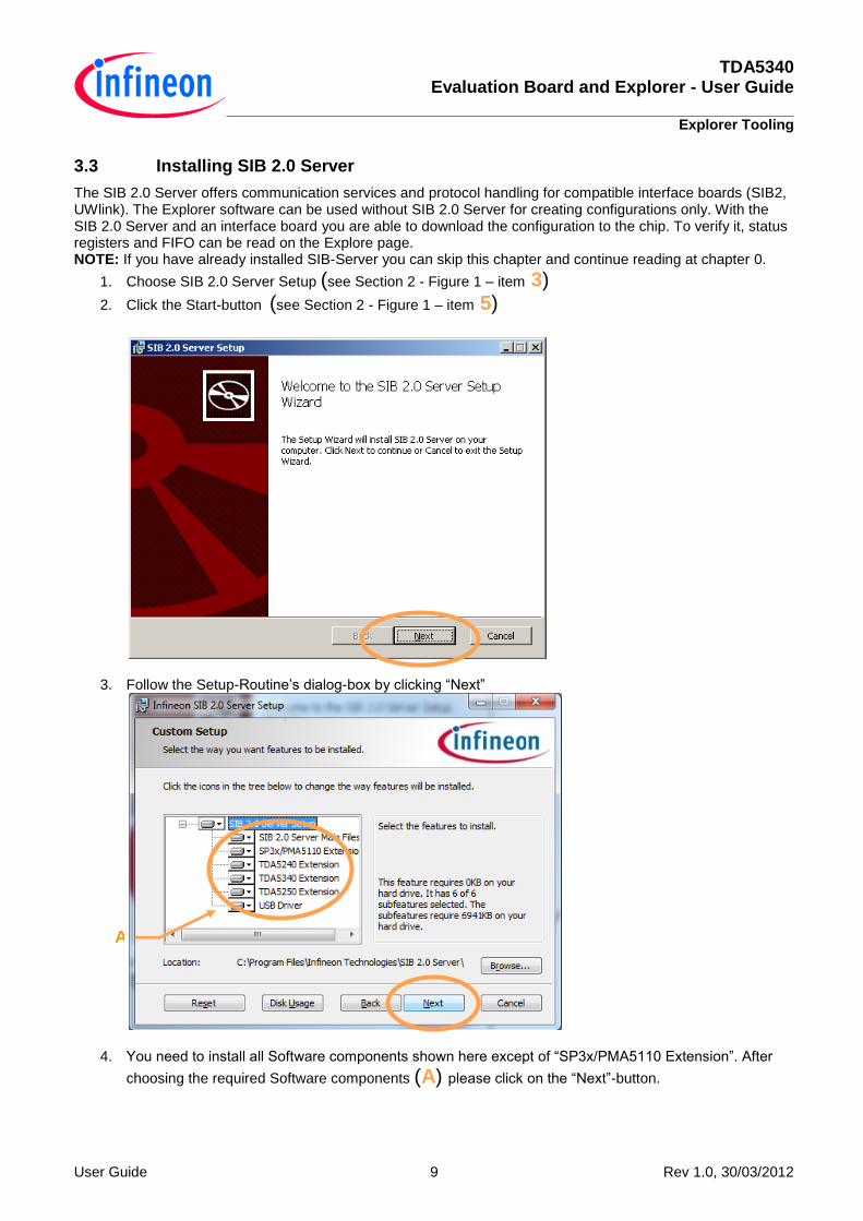
3.3 Installing SIB 2.0 Server
The SIB 2.0 Server offers communication services and protocol handling for compatible interface boards (SIB2, UWlink). The Explorer software can be used without SIB 2.0 Server for creating configurations only. With the SIB 2.0 Server and an interface board you are able to download the configuration to the chip. To verify it, status registers and FIFO can be read on the Explore page. NOTE: If you have already installed SIB-Server you can skip this chapter and continue reading at chapter 0.
1. Choose SIB 2.0 Server Setup (see Section 2 - Figure 1 – item 3)
2. Click the Start-button (see Section 2 - Figure 1 – item 5)
3. Follow the Setup-Routine‟s dialog-box by clicking “Next”
4. You need to install all Software components shown here except of “SP3x/PMA5110 Extension”. After
choosing the required Software components (A) please click on the “Next”-button.
A

TDA5340 Evaluation Board and Explorer - User Guide
Explorer Tooling
User Guide 10 Rev 1.0, 30/03/2012
5. Click on the “Install”-Button to install the software on your computer
6. Setup will be completed by clicking the “Finish”-Button

TDA5340 Evaluation Board and Explorer - User Guide
Explorer Tooling
User Guide 11 Rev 1.0, 30/03/2012
3.4 SibServer DLL
The Installed Sib server may have not the latest Software plug in to run the TDA5340 Explorer. This Chapter will guide you through the steps to update your SibServer with the latest Software plugins.
1. Close the SiB Server if it is running.
2. Copy from the Explorer installation folder SibServerPlugin the content to the SibServer installation folder
3.5 User Interface and Getting Started
To start configuration utility choose the application loader executable (NextGenLoader.exe) from the start menu (Start -> Programs -> Infineon Technologies -> Configuration Utility Loader). The loader pad offers a runtime environment for installed applications. Optionally it is possible to start the Explorer directly via the start menu by using the shortcut in the TDA Explorer subfolder (Start -> Programs -> Infineon Technologies -> TDA5340 -> TDA53xx Explorer).

TDA5340 Evaluation Board and Explorer - User Guide
Explorer Tooling
User Guide 12 Rev 1.0, 30/03/2012
3.5.1 Infineon Evaluation Software Startup Screen
Figure 3 Figure 1: NEXTGENLOADER
1. Close-Button
2. Minimize-button
3. SIB 2.0 Server Setup
4. TDA5340 Explorer
5. Start-Button
3.5.2 Starting Explorer
1. Choose “TDA5340 Explorer” on the NEXTGENLOADER pad (4)
2. Click the Start-button (5)
3. A splash-screen is displayed during application loading
1
2
3
4
5

TDA5340 Evaluation Board and Explorer - User Guide
Explorer Tooling
User Guide 13 Rev 1.0, 30/03/2012
3.6 TDA5340 Explorer Tooling description
Figure 4 Figure 2: General Start page / main tabs
1. General tab: general chip settings
2. TX tab: only visible if one of the configurations is used in TX Mode!
3. RX tab: only visible if one of the configurations is used in RX Mode!
4. Registers tab (see chapter 3.6.8)
5. Explore tab (see chapter 3.6.7)
6. LOG tab: for viewing the log-file (Chapter 4)
7. About tab
7
1
2
3
4
5
6

TDA5340 Evaluation Board and Explorer - User Guide
Explorer Tooling
User Guide 14 Rev 1.0, 30/03/2012
3.6.1 Getting additional information about available functions
Figure 5 Figure 3: Valuable Functions - Tooltips
Many input and output fields will give additional tooltip information, a while after moving the cursor over this field. This function is available on the Wizard-Tab, on the Register-Tab and on the Explore-Tab.

TDA5340 Evaluation Board and Explorer - User Guide
Explorer Tooling
User Guide 15 Rev 1.0, 30/03/2012
3.6.2 General Chip Control
Figure 6 Figure 4: General Control
1. SIB & Evaluation board selection
2. Virtual status indication LED
3. Register control buttons
Note:
Functions from the Chip control selection (1) can be chosen from
“SIB2 menu bar”.
Functions from the Register control buttons (3) can be chosen from “Register menu bar”.
The address format of the evaluation hardware is defined as follows: SIB2::<master board ID>::<sub board ID> If the master-board should be addressed directly the sub-board ID has to be replaced by the key “BOARD”.
2 1
3

TDA5340 Evaluation Board and Explorer - User Guide
Explorer Tooling
User Guide 16 Rev 1.0, 30/03/2012
3.6.2.1 Sib Server / Evaluation board detection
If the desired Evaluation board is not detected correctly or the connection is lost the following instructions will establish a new connection to the evaluation board.
Note: The TDA5340 will be default configuration set due to a hardware reset.
Do a right mouse click on the SIB icon in the Task bar (see picture below) and select “Recreate Device List”
Afterwards the detection of the master board and Sub board should be successful. If not the Evaluation board should be disconnected from the USB and connected again. The “Recreate Device List” action should be performed again.
In case if the TDA5340 Explorer is already running with a modified configuration set. The chip control should be closed and opened again.
3.6.2.2 Chip Control
Choose your sub-board from the chip control-Selection combo-box (1). If a SIB board is connected when
the Explorer runs already you have to press the Refresh button to update the combo-box.
3.6.2.3 SIB (System Interface Board) Status
Press the “Open”-Button. If the virtual LED (2) turns from red to green, your board will be ready to use.
Communication with the chip is only possible when opening a sub-board device (sub board ID must not be “BOARD”). A sub board can be identified by the sub-board serial key.
The SIB connection procedure performs following operations:
Establishing a connection to the SIB server. If the SIB server process is not started, it will be started now. If the SIB server start takes longer than the Explorer start or a UWLink board has been connected after starting the Explorer you may have to refresh the device list by pressing the “Refresh” button
The UWLink hardware is verified. If a wrong sub-board is connected or an outdated SIB server plug-in for the target device is installed, the connection fails. If you are sure about using the correct firmware, please try to plug the sub-board off and on to force a firmware update and press the “Refresh” button followed by the “Open” button again.
After the connection to the UWLink hardware has been established successfully, the message “Device SIB2::MASTERBD::SUBBOARD/TDA53xx initialized” will be displayed. The chip variant is being verified and compared to the running Explorer variant. If the chip variant does not match the

TDA5340 Evaluation Board and Explorer - User Guide
Explorer Tooling
User Guide 17 Rev 1.0, 30/03/2012
running Explorer variant, a correct operation is not guaranteed and a warning will be displayed in the SIB status box.
A message box appears and you will be asked whether you want to reload the actual Explorer configuration to the chip. Choose “Yes” to download the settings of the actual configuration. This will bring the chip to a state where its settings represent exactly the settings of the Explorer software. If you choose “No” the chip will be reset, but no configuration is transferred to it. The configuration of the Explorer will be set to the default register settings. Any former setting gets lost unless you saved it to a SPI configuration file.
When downloading the register settings the first time, a set of registers is written additionally to these which were affected by the settings you made. These registers are listed in the chapter 3.7 (Register patch list) and they are written to equalize the default state of hardware and software. All write operations done by the Explorer are mapped to the SPI configuration file, therefore all settings you produce while experimenting using the Explorer are available in the output file regardless how often you change and download a setting to the chip.
3.6.2.4 Updating Registers
Changes in the configuration can be transferred to the chip by pressing the “Write Registers” button. If there is any difference in the actual configuration between the user interface and the hardware, the LED “Updated” indicated this by a red color. After a successful update of the registers the color of the LED changes to green. If the color of the LED is dark grey, a connection to the evaluation hardware is not yet established.
The default download mode for writing registers uses the SPI burst command. All differences of registers between the user interface and the chip are grouped block wise and a SPI burst command is executed for each block separately. If an initial switch to the sleep/hold mode is necessary a separate standard SPI write command is used. You can force the usage of standard SPI write commands for all registers by un-checking the “Use Burst Mode” checkbox. The content of read-only registers can be updated by pressing the “Read Registers” button. All controls in the configuration user interface that represents the content of a read-only register will be updated automatically and the register list in the “Registers” tab will be set to the new values.
Important: Only read-only registers are affected, you cannot perform read operations on writeable register!

TDA5340 Evaluation Board and Explorer - User Guide
Explorer Tooling
User Guide 18 Rev 1.0, 30/03/2012
3.6.3 Tab Navigation Hints
If you are running this software for the first time it is recommended to use the RX/TX and General tab to generate your first configuration. Please apply the sub tabs in sequential order because input values of following sub tabs can depend on values from previous tabs. The Explorer offers you easy access to the registers of the and makes your first steps more comfortable.
Figure 7 Figure 5: Control Hints
1. Subtab selection
2. Configuration selection tab
The has a multi-configuration capability. Some register settings describe the same functions, but they take effect only if the configuration they belong to becomes active. In the sub tabs all configuration-dependent settings are framed by a configuration selection tab. The tab header changes in dependency of the active configurations. Whenever you change the active page of the configuration tab (2) the content of the tab page is updated to the settings of the new configuration selection. Switching to another sub tab retains the active configuration. Calculations which forces recalculations on other sub tabs than the active one are performed for the actual configuration only.
Some sub tabs offer interactive configuration support, which will be described in detail for each page of the sub tab. These are features like automatic enabling/disabling of controls in dependency of different operating mode, appliance of limits, calculations and dependency updates over multiple sub tabs. In the
1
2

TDA5340 Evaluation Board and Explorer - User Guide
Explorer Tooling
User Guide 19 Rev 1.0, 30/03/2012
following subsections for each sub tab the available calculations and dependencies are explained in the associated paragraphs.
The data management of the Explorer configuration software is concentrated at the register grid on the Registers tab. Individual sub tabs communicate with the register grid to exchange register content. Whenever the content of the register grid changes, the affected controls will be automatically updated (passive dependencies).
Note: It is not recommended to apply manual changes on the Register Tab, as these changes are not subject to input validation. Otherwise inconsistent settings might be generated.
Beside this data exchange the necessity of reacting to the change of input variables of calculations is given. These changes have impact on registers and the result of a calculation can have impact to registers on other sub tabs. Whenever an input variable of a calculation targets a register setting of another sub tab, a calculation will be initiated automatically (active dependency).
To restore a configuration, loading the register values of the is not enough. Due to the fact that several calculation inputs have impact on a set of registers to summarize the complexity of the registers, these inputs cannot be reproduced from the register values directly. To guarantee exact restoring of the saved configuration such input variables are stored separately in the configuration file (3.6.9) as persistent variables (for each configuration by appending A/B/C/D to the variable name). Beside numeric values (e.g. data-rate) also textual values will be stored (e.g. TSI pattern name) in the configuration file. Existing persistent variables are described in the chapter of the corresponding sub tabs.
3.6.4 General Tab
3.6.4.1 Main Configuration
Figure 8 Figure 6: General tab / Main Configuration sub tab
Within this Main Configuration the usage of the different Configuration sets of the TDA5340 is defined. The operating mode choices are RX, TX and Not Used. If no configuration is set to RX or TX also the corresponding main tab is hidden.
Be aware if the receiver should work in self polling mode, the RX configurations must start at Configuration A and have to be concatenated.

TDA5340 Evaluation Board and Explorer - User Guide
Explorer Tooling
User Guide 20 Rev 1.0, 30/03/2012
3.6.4.2 Crystal Oscillator and System Clock
Figure 9 Figure 7: General – Crystal Oscillator and System Clock
This sub-tab allows you to configure:
XTAL Calibration / Trimming for fine trimming the crystal frequency
External Clock Generation
For information beyond the quick help / tooltip (moving the mouse pointer on a selected item) refer to the datasheet / manual.
TDA5340 Evaluation Board and Explorer - User Guide
Explorer Tooling
User Guide 21 Rev 1.0, 30/03/2012
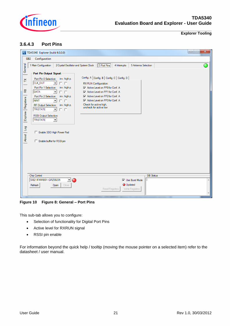
3.6.4.3 Port Pins
Figure 10 Figure 8: General – Port Pins
This sub-tab allows you to configure:
Selection of functionality for Digital Port Pins
Active level for RXRUN signal
RSSI pin enable
For information beyond the quick help / tooltip (moving the mouse pointer on a selected item) refer to the datasheet / user manual.
TDA5340 Evaluation Board and Explorer - User Guide
Explorer Tooling
User Guide 22 Rev 1.0, 30/03/2012
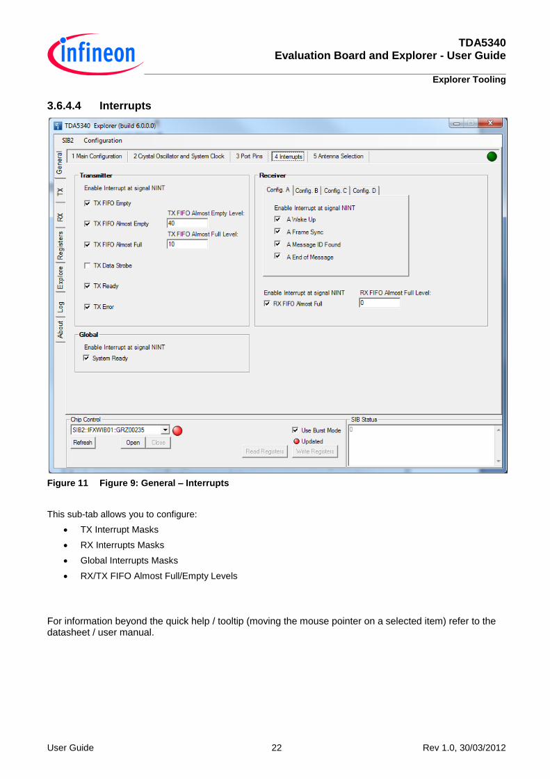
3.6.4.4 Interrupts
Figure 11 Figure 9: General – Interrupts
This sub-tab allows you to configure:
TX Interrupt Masks
RX Interrupts Masks
Global Interrupts Masks
RX/TX FIFO Almost Full/Empty Levels
For information beyond the quick help / tooltip (moving the mouse pointer on a selected item) refer to the datasheet / user manual.

TDA5340 Evaluation Board and Explorer - User Guide
Explorer Tooling
User Guide 23 Rev 1.0, 30/03/2012
3.6.4.5 Antenna Selection
Figure 12 Figure 10: General – Antenna Selection
This sub-tab allows you to configure:
The position of the internal and external antenna switches for RX and TX Mode
Antenna Diversity on RSSI (ADR) switching thresholds and freeze conditions
For information beyond the quick help / tooltip (moving the mouse pointer on a selected item) refer to the datasheet / user manual.

TDA5340 Evaluation Board and Explorer - User Guide
Explorer Tooling
User Guide 24 Rev 1.0, 30/03/2012
3.6.5 RX Tab
3.6.5.1 Master Control
Figure 13 Figure 11: RX 1 - Master Control Unit
This tab allows you to configure:
Modulation type selection
RX FIFO options
RF/IF Front End
For information beyond the quick help / tooltip (moving the mouse pointer on a selected item) refer to the official datasheet.
Dependencies
The Digital RX tab depends on the Master Control Unit. A change of the modulation type selection or a change of the external data processing selection has an impact on the calculation of the register values for the data-rate. At least one of the port pins must be set to output “DATA” to make the setting for the raw data slicer available on Digital RX tab. The buttons “Force

TDA5340 Evaluation Board and Explorer - User Guide
Explorer Tooling
User Guide 25 Rev 1.0, 30/03/2012
EOM” and “Force TOTIM” on the Explore page are operational only if external data processing is set to “Chip Data” or “MF Data”.
Interactivity
The available configurations and modulation types depend on the selected operating mode. Only the currently possible configurations and modulation types are visible and enabled. If the option “Lock Data FIFO at EOM” is checked, the option “Init of FIFO at Cycle Start” gets inactive and vice versa.
3.6.5.2 RF PLL
Figure 14 Figure 12: RX 2 - RF PLL
This sub-tab allows you to configure:
RF PLL channels
Conversion Mode and LO injection side
PLL loop filter settings (PLL bandwidth)
For information beyond the quick help / tooltip (moving the mouse pointer on a selected item) refer to the official datasheet.

TDA5340 Evaluation Board and Explorer - User Guide
Explorer Tooling
User Guide 26 Rev 1.0, 30/03/2012
Dependencies
This page does not have direct dependencies on other pages - excepting the visibility of channels (the operating mode selection has impact on the number of active channels).
Calculations
This page allows you to configure the SD-PLL just by entering the desired frequency in one of the textboxes for up to three channels. The results are displayed on the “Registers” tab at the corresponding registers. Consider that all active channels must be set to a frequency within the same frequency band. If this is not the case, the application will indicate it with the “Out of band” LED.
Switching the sideband or conversion selection also initiates a recalculation of the RF settings.
The input frequency is compared to the selected sideband and a warning message will be displayed next to the frequency input textbox if the optimal sideband is not chosen.
Interactivity
Some input fields for the frequency are hidden if they are not needed in the actual configuration. If you enter an input frequency, the band selection is set automatically, but only when all active channels are set to a valid frequency within the same frequency band. If you change the actual frequency band selection and the active channels are not located within the new band, the frequency of all channels is set to the default value of the new frequency band.

TDA5340 Evaluation Board and Explorer - User Guide
Explorer Tooling
User Guide 27 Rev 1.0, 30/03/2012
3.6.5.3 Digital RX
Figure 15 Figure 13: RX 3 - Digital Receiving Unit
This sub-tab allows you to configure:
Datarate
Resulting FSK/ASK Settings
Filter Settings
RSSI Slope and Offset Compensation
Peak Memory Filter (PMF)
RAW Data Slicer (DATA output)
Digital Receiver functions
For information beyond the quick help / tooltip (moving the mouse pointer on a selected item) refer to the official datasheet.
Dependencies

TDA5340 Evaluation Board and Explorer - User Guide
Explorer Tooling
User Guide 28 Rev 1.0, 30/03/2012
The RX RX 9 - AGC AFC depends on the RX RX 3 - Digital Receiving Unit.
Most calculations on this page and enabling/disabling of some controls depend on the selected modulation type on page RX RX 1 - Master Control Unit.
Calculations
By entering a value in the data-rate field the recalculation of all related registers is initiated. A new value becomes valid when you enter the data-rate and press the return key afterwards, when you change the data-rate by pressing the up or down button, or if you entered the data-rate and the input field looses the focus. The calculation is not done during entering number in the data-rate field.
Input variables for the data-rate calculation are:
The data-rate input field
The chips-per-bit switch
The modulation type setting
Analog and digital filter settings
External processing selection (DATA (matched filter) output mode)
Changing one of the input variables for the data-rate calculation will also force a recalculation.
The automatic calculation of the best fitting digital filter bandwidth is done by default. If you want to select the digital filter bandwidth manually you have to uncheck the “Auto Configure Filters” checkbox.
The settings of the RSSI slope and RSSI offset compensation are translated to the corresponding register values.
Calculating the peak memory filter is supported in two directions. You can either enter the desired attack and decay time in dimensions of bit or you can select the attack and decay factor. When auto configuring is enabled, entering a time will configure the proper factor in respect of the actual data-rate. The best factor will be chosen although the entered time may not fit the calculated factor ideally. Only the value for the attack and decay factor is saved and not the value of the attack and decay time. Therefore whenever this wizard page is opened again, the values for the attack and decay time will be back calculated. This may cause slightly different time values than you have entered before.
Interactivity
The input fields for the configuration of the signal and noise detector will be enabled or disabled in dependency of the selected signal and noise detector mode. Settings not needed for configuring the selected mode will be disabled and are not accessible.
The raw data slicer group-box is displayed only if at least one of the port pins is set to the output signal “DATA”.
The anti-aliasing-filter can be configured only if automatic filter configuration is disabled and the anti-aliasing filter is not bypassed for the RSSI pin.
If the actual filter and data-rate setting does not follow the Carson bandwidth rule, an alert message box pops up.
Persistent variables
Beside the content of the registers affected by this page, these inputs will be stored additionally in the configuration file:
CHIPSPERBIT: Chips per bit selection below the data-rate input field (default is 2 chip/bit)
AUTOCONF: Activation of auto-filter-configuration (default is activated)

TDA5340 Evaluation Board and Explorer - User Guide
Explorer Tooling
User Guide 29 Rev 1.0, 30/03/2012
FDEV: Expected max. FSK deviation (default is +/- 64 kHz)
FDEVMIN: Expected min. FSK deviation (default is +/- 10 kHz)
DATARATE: Data-rate input (default is 2000 bit/s)
Wizard_4_Digital_Receiving_UnitAUTOCONF: Automatic configuration of filters in the analog and digital frontend (default is enabled)
Wizard_5_RF_IF_FrontendAUTOCONF: Automatic configuration of peak memory filter attack and decay time (default is enabled)
AUTOCONF_SLICER: Automatic configuration of the RAW data slicer (default is enabled)
STIME: Settling time of RAW data slicer (default is 15 bit)
3.6.5.4 Signal Recognition
Figure 16 Figure 14: RX 4 – Signal Recognition
This sub-tab allows you to configure:
Signal Recognition Thresholds (Signal Detector, FSK Noise Detector)

TDA5340 Evaluation Board and Explorer - User Guide
Explorer Tooling
User Guide 30 Rev 1.0, 30/03/2012
3.6.5.5 Clock Data Recovery
Figure 17 Figure 15: RX 5 - Clock Data Recovery (CDR)
This sub-tab allows you to configure:
P Loop configuration
I Loop Configuration
CDR Runin & Dutycycle / Data rate acceptance
Maximum number of code violations
Zero Tube / Slicer
For information beyond the quick help / tooltip (moving the mouse pointer on a selected item) refer to the official datasheet.
Dependencies
This page does not have dependencies on other pages - excepting the TSI settings of RX6- Framer that influences the result of the timing violation window length register.
2
1
TDA5340 Evaluation Board and Explorer - User Guide
Explorer Tooling
User Guide 31 Rev 1.0, 30/03/2012
Calculations
The time violation window length register value will be calculated according to the formula in the official datasheet. Inputs of the calculation are the TSI mode (existence of a gap), the user input for the maximum length of a code violation within a data-packet and the number of equal bits (code violations) at the end of the TSI pattern.
Interactivity
For this page predefined „easy‟ settings exist that cover most of all common protocol scenarios, so the
complexity of the CDR configuration is broken down to three possible settings (2). This „easy‟ mode is the recommended default mode for this unit. If you want to configure the CDR manually the page mode can be
changed from easy to advanced (1).
The two extremes are:
Fast: For high data-rate and duty-cycle variations; long gaps within the protocol
Slow: For high accuracy in data-rate and duty-cycle; at least 6 bit run-in required
Whenever you change to this page, the actual settings are compared to the presets and if one of the
presets matches the option box (2) is set to this preset. This means, if you change a CDR setting manually in the registers tab or in a SPI configuration file, the corresponding preset will be detected automatically. If no preset fits the actual setting the page mode changes from easy to advanced.
Persistent variables
Beside the content of the registers affected by this page, these inputs will be stored additionally in the configuration file:
CV: Maximum length of code violation within data-packet (default is 1 bit)

TDA5340 Evaluation Board and Explorer - User Guide
Explorer Tooling
User Guide 32 Rev 1.0, 30/03/2012
3.6.5.6 Frame Synchronization Unit (Framer)
Figure 18 Figure 16: RX 6 - Frame Synchronization Unit (Framer)
This sub-tab allows you to configure the TSI modes:
16 Bit TSI Mode
8 Bit Parallel TSI Mode
8 Bit Extended TSI Mode
8 Bit TSI Gap Mode
For information beyond the quick help / tooltip (moving the mouse pointer on a selected item) refer to the official datasheet.
Dependencies
This page does not have dependencies on other pages.
Calculations
For the 8 Bit TSI Gap Mode the value of the gap-time register will be calculated from the entered time in units of bit. The register can be configured manually by checking the override manually checkbox.

TDA5340 Evaluation Board and Explorer - User Guide
Explorer Tooling
User Guide 33 Rev 1.0, 30/03/2012
Interactivity
The active TSI mode can be selected by switching to a tab page. The selected tab page defines the active TSI mode. The patterns for the different TSI modes are stored separately during run-time. Only data of the active TSI mode is saved in the configuration file (see Registers tab). That means that you can configure a TSI mode and then change pattern of another TSI mode without touching the configuration of the previous TSI mode, even if the same register has been modified. The configuration of a TSI mode page will be reloaded when you switch to the page. If actually no configuration was done for the TSI mode page you selected (so the page was never selected before), the default register values will be used to fill the input controls. The output field Pattern (A/B) summarizes the entered TSI configuration and displays the expected TSI pattern.
Persistent variables
Beside the content of the registers affected by this page, these inputs will be stored additionally in the configuration file:
PROTOCOL_NAME: Name of the protocol input field (default is empty)
PATTERN16: 16 bit TSI mode pattern
PATTERNA1: 8 bit parallel TSI mode pattern A
PATTERNB1: 8 bit parallel TSI mode pattern B
PATTERNA2: 8 bit TSI gap mode pattern A
PATTERNB2: 8 bit TSI gap mode pattern B
PATTERNA3: 8 bit extended TSI mode pattern A
PATTERNB3: 8 bit extended TSI mode pattern B
GAPTIME: Transmitted gap time input field for TSI gap mode (default is zero)
TSIGAPOVERRIDE: Override checkbox to enabled TSI gap register values manually (default is unchecked)
TSILENA: TSI length for TSIA
TSILENB: TSI length for TSIA
WCA: Wildcards at the end of TSIA
DLLIMIT: Payload Data Length Limit for TSIA
DLLIMITB: Payload Data Length Limit for TSIB
The TSI patterns are stored as persistent variables to allow comfortable entering of different TSI modes for testing purpose during run-time of the software. Patterns are stored independently of the entered TSI length. It is allowed to enter different patterns for different TSI modes, but only the pattern information for the active TSI mode will be store to a configuration file. The TSI pattern for the active TSI mode is reflected in the register settings. On a change of the TSI mode the affected registers are set to the new values. If no pattern information was found in the loaded configuration file, the default value for the TSI pattern will be set using the TSI pattern register content.

TDA5340 Evaluation Board and Explorer - User Guide
Explorer Tooling
User Guide 34 Rev 1.0, 30/03/2012
3.6.5.7 Message ID
Figure 19 Figure 17: RX 7 - Message ID
This sub-tab allows you to configure:
Message IDs with different Byte Organization modes
For information beyond the quick help / tooltip (moving the mouse pointer on a selected item) refer to the official datasheet.
Dependencies
This page does not have dependencies on other pages.

TDA5340 Evaluation Board and Explorer - User Guide
Explorer Tooling
User Guide 35 Rev 1.0, 30/03/2012
3.6.5.8 Timer Unit
Figure 20 Figure 18: RX 8a - Timer
This sub-tab allows you to configure:
ON and OFF Timing
Timer for autonomous chip operation mode
For information beyond the quick help / tooltip (moving the mouse pointer on a selected item) refer to the datasheet / user manual.
Dependencies
The number of selected RF channels per configuration has influence to the calculated polling period.
The value for register SYSRCTO is calculated from the selected number of RUNIN chips from RX 5 – Clock Data Recovery.
Calculations

TDA5340 Evaluation Board and Explorer - User Guide
Explorer Tooling
User Guide 36 Rev 1.0, 30/03/2012
This page integrates calculations for the polling timer unit, the register values for the wake-up level observation time, the Sync Search Time-out and the time-out timers.
The input field of the timing group allows you to configure the on/off-timing, whereas these timer values are multiple of the reference timer. If the reference timer changes, the values for the on-time are set to the next higher time that fits and the value for the off-time is set to the next lower time that fits. The resulting polling period field shows the time TMasterPeriod which is calculated as described in the figures of the Polling Timer Unit chapter of the official datasheet.
Interactivity
The on-time input fields are displayed in dependency of the active configurations and the selected self polling mode.
The available input field of the wake-up detection group depends on the selection of the wake-up criterion and if a data criterion is selected also on the activation of ultra-fast fallback to sleep.
3.6.5.9 Wakeup Unit
Figure 21 Figure 19: RX 8b – Wake up
This sub-tab allows you to configure:
Self Polling Mode
Wake up detection

TDA5340 Evaluation Board and Explorer - User Guide
Explorer Tooling
User Guide 37 Rev 1.0, 30/03/2012
For information beyond the quick help / tooltip (moving the mouse pointer on a selected item) refer to the datasheet / user manual.
Dependencies
This page does not have dependencies on other pages.
Interactivity
The available input field of the wake-up detection group depends on the selection of the wake-up criterion and if a data criterion is selected also on the activation of ultra-fast fallback to sleep.
3.6.5.10 AGC AFC
Figure 22 Figure 20: RX 9 - AGC AFC
This sub-tab allows you to configure:
AFC (Automatic Frequency Control) Settings
AGC (Automatic Gain Control) Settings

TDA5340 Evaluation Board and Explorer - User Guide
Explorer Tooling
User Guide 38 Rev 1.0, 30/03/2012
For information beyond the quick help / tooltip (moving the mouse pointer on a selected item) refer to the official datasheet.
This page is the last page of the wizard. If this page is reached the configuration is ready to be written to the chip. This can be done by pressing the “Write Registers” button in the chip control area.
Dependencies
The data-rate setting of RX 3 – Digital RX is used for the calculation of the AFC filter coefficients.
Calculations
If the auto-configuration of the AFC filters is activated you can configure the AFC filter coefficients by choosing one of the predefined settling time values.
Interactivity
Changes of the AFC/AGC settings can be done only if the AFC/AGC unit is not switched off.
Persistent variables
Beside the content of the registers affected by this page, these inputs will be stored additionally in the configuration file:
AUTOCONF: Automatic configuration of AFC filter setting enable (default is enabled)
ST: AFC filter settling time (default is fast)
TDA5340 Evaluation Board and Explorer - User Guide
Explorer Tooling
User Guide 39 Rev 1.0, 30/03/2012
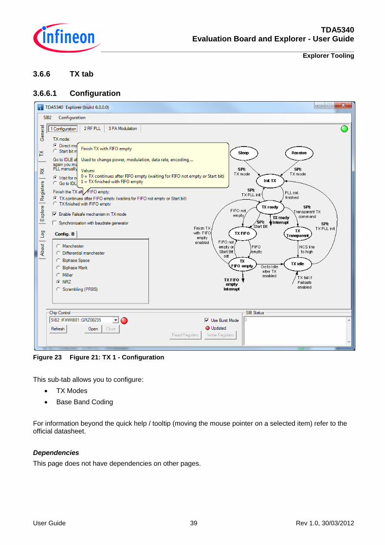
3.6.6 TX tab
3.6.6.1 Configuration
Figure 23 Figure 21: TX 1 - Configuration
This sub-tab allows you to configure:
TX Modes
Base Band Coding
For information beyond the quick help / tooltip (moving the mouse pointer on a selected item) refer to the official datasheet.
Dependencies
This page does not have dependencies on other pages.

TDA5340 Evaluation Board and Explorer - User Guide
Explorer Tooling
User Guide 40 Rev 1.0, 30/03/2012
3.6.6.2 RF PLL
Figure 24 Figure 22: TX 2 – RF PLL
This sub-tab allows you to configure:
RF Bands and Channels
PLL Loop Filter Bandwidth
PLL Lock Dectector
For information beyond the quick help / tooltip (moving the mouse pointer on a selected item) refer to the official datasheet.
Dependencies
This page does not have dependencies on other pages.

TDA5340 Evaluation Board and Explorer - User Guide
Explorer Tooling
User Guide 41 Rev 1.0, 30/03/2012
3.6.6.3 PA Modulation
Figure 25 Figure 23: TX 3 – PA Modulation
This sub-tab allows you to configure:
TX Data Rate
Modulation Schema
PA Output Stages (Output power)
For information beyond the quick help / tooltip (moving the mouse pointer on a selected item) refer to the official datasheet.
Dependencies
This page does not have dependencies on other pages.
3.6.7 Explore
The Explore tab integrates basic functionality for interactive chip control. In contrast to the main tab pages a reasonable usage of the Explore page is possible with connected evaluation hardware only.
TDA5340 Evaluation Board and Explorer - User Guide
Explorer Tooling
User Guide 42 Rev 1.0, 30/03/2012
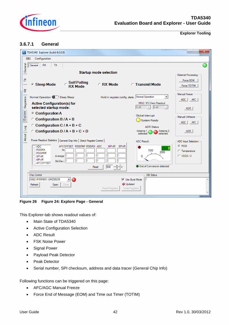
3.6.7.1 General
Figure 26 Figure 24: Explore Page - General
This Explorer-tab shows readout values of:
Main State of TDA5340
Active Configuration Selection
ADC Result
FSK Noise Power
Signal Power
Payload Peak Detector
Peak Detector
Serial number, SPI checksum, address and data tracer (General Chip Info)
Following functions can be triggered on this page:
AFC/AGC Manual Freeze
Force End of Message (EOM) and Time out Timer (TOTIM)

TDA5340 Evaluation Board and Explorer - User Guide
Explorer Tooling
User Guide 43 Rev 1.0, 30/03/2012
Readout
The controls are updated on each press of the “Read Registers” button in the chip control area. Reading registers is possible with connected and opened evaluation hardware only. You can perform a continuous readout of the registers shown within the Readout group-box by checking the box “Continuous readout”. Continuous readout is stopped by uncheck the box or when the interface board connection has been closed.
Power Readout Statistics
This section provides statistical information on different selectable signal sources (e.g. Signal and Noise Power SPWR, NPWR). All registers check marked in the list on the left side will be read.
By pressing the “Read” button the selected count of readings of the selected power readout registers are done and the average and standard deviation of the results are displayed (readout may take some time!). This can be used for evaluation of threshold values. For further information about using those results to configure the signal and noise detector refer datasheet or refer to the application note for signal and noise detector threshold settings.
Direct Register Control
In this area registers can be directly addressed. You can either read or write a single register, or you can enter a sequence of registers that should be written in one run.
To verify the success of a single register write operation change to the general chip info tab and press the “Read Registers” button in the Chip Control section. The address and data tracer registers will display the recently written address and value.
Sequences for batch write operations consist of one or more lines of a register name followed by the register value and delimited by a colon (<address:value>). The result of a batch write operation is shown in the SIB status box.
A direct register write access does also an update of the register grid in the Registers tab and this in succession initiates an update of all affected controls in the configuration interface.
Note: Manual changes in the register list are allowed in principle, but not subject to input validation, therefore an inconsistent setting might be generated!

TDA5340 Evaluation Board and Explorer - User Guide
Explorer Tooling
User Guide 44 Rev 1.0, 30/03/2012
3.6.7.2 RX
Figure 27 Figure 25: Explore Page - RX
This Explorer-tab shows readout values of:
FSK Noise Power
Signal Power
Payload Peak Detector
Peak Detector
Interrupts of Receiver portion
Run Section
This group can be used to simulate a simple application case. When starting the interrupt detection, the correct NINT port pin will be configured from the actual configuration. Press the switch to turn the interrupt detection on. Whenever an interrupt is recognized by the interface board, the counter “Received interrupts” increases and a readout of the interrupt status registers is done. If at least one configuration indicates an end of message, the FIFO of the TDA5340 is read and the payload peak value in the corresponding textbox is updated. A successful read FIFO operation is indicated by increasing the “Processed messages” counter. The resulting data of the read FIFO operation is displayed in textbox as HEX string (“0x”) and the

TDA5340 Evaluation Board and Explorer - User Guide
Explorer Tooling
User Guide 45 Rev 1.0, 30/03/2012
same data is displayed as binary string (“0b”). It is possible to compare the incoming data with a predefined payload pattern. Just enter the expected payload in the corresponding textbox in hexadecimal format and specify the number of bits of the incoming data. If a data packet has been received, it will be compared automatically and the result of the comparison is visualized by an increment of the “Correctly received payload data” counter on success. Up to 512 incoming packets can be buffered by the Explorer software. The packet history can be reviewed by selecting a packet in the received packets combo-box.
3.6.7.3 TX
Figure 28 Figure 26: Explore Page - TX
This Explorer-tab shows readout values of:
Interrupts of Transmitter section
And also input values for
TX FIFO almost full and empty levels
o Depending Data Rate the almost empty level must be adjusted to give the interface time to reload the data.
o 10-20 if data rate is up to 10kBit
o 20-50 if data rate is up to 100kBit

TDA5340 Evaluation Board and Explorer - User Guide
Explorer Tooling
User Guide 46 Rev 1.0, 30/03/2012
Following functions can be triggered on this page:
Initialization of TX FIFO
Initialization of PLL
Sent TX start bit
Load TX FIFO with predefined data pattern
Send PRPS stream (generates random Data)
Transmit Continuous Wave (generates all one Data)
o Note: is only CW if Coding is set to NRZ!
3.6.8 Registers Tab
1. Register view/(selection) area
2. Scroll bar
3. File Control
4. Find register area
Figure 29 Figure 27: Registers Tab
1 2
3
4

TDA5340 Evaluation Board and Explorer - User Guide
Explorer Tooling
User Guide 47 Rev 1.0, 30/03/2012
3.6.8.1 Register Selection Area (Register Grid)
This area gives you full access to all available registers. Each marker (checkbox for a bit) can be set or deleted by clicking on it. All changes you make in the wizard will also be made in the register tab and vice versa.
Note: Manual changes in the register list are allowed in principle, but not subject to input validation, therefore an inconsistent setting might be generated!
The register grid offers you several possibilities to perform settings and access registers.
Grid sort: Click the header of a column to sort the registers by name or address
Leave the mouse pointer above a column of the grid to popup a tooltip containing the full name of the register
Double-click the content of the “Value” column to enter the edit mode of the value of a register. Enter a valid hexadecimal number (in c-style format, with a leading 0x) to set the register to a new value.
Click into the columns 0 to 7 to change a single bit of a register. The hexadecimal value field will be updated automatically.
Whenever a register value is changed on one of the wizard pages the pointer in the register list is set to the corresponding register address. You can check the setting by switching from the wizard page to the register page after entering a value on a wizard page. If an input forces a calculation and/or more than a single register is affected, then the pointer marks the last register that was affected by the operation.
3.6.8.2 Scroll Bar
The register set is very large, scroll up and down in normal Microsoft Windows behavior.
3.6.8.3 File Control
Saving and loading of register sets can be done here. You have several options by selecting the drop down menu:
Save Active All differences between the active configurations (A, B, C, D) of the setting and the reset values of the chip are saved. Only patched registers of the active configurations will be saved. When reloading a configuration that has been save using this mode the patched registers for the inactive configurations are merged with the loaded registers.
Note: When using the operating mode run-mode slave only the actual active configuration will be saved. If more than one configuration is used, it is recommended to use the save modes “Save Difference” or “Save All” to preserve all settings.
Save Difference All differences between the actual setting and the reset values of the chip are saved. It will not be considered whether a configuration is active or not active in this setting. This method includes all patched registers as listed in the appendix.
Save All All registers displayed in the register list are saved.
Save configuration page (_A_, _B_, _C_, _D_)
All registers of a specific configuration are saved, even if they are not touched by the actual setting. This mode can‟t be used to retrieve an operational SPI configuration.
Regardless of the save mode selection the chip mode control register is written as first (sleep mode) and as last write command of the output file.

TDA5340 Evaluation Board and Explorer - User Guide
Explorer Tooling
User Guide 48 Rev 1.0, 30/03/2012
A short description for the configuration can be entered in the textbox below the file selection box.
To open a configuration from a file press the left button, to save a configuration to a file press the right button. In the appearing open or save file dialog box the path and name of the target file can be selected.
Choose the desired type of file using the “Files of type” or the “Save as type” dropdown box. Enter a filename or select a file in the pane above to open or save a configuration.
These types of configuration files are supported:
_spi.def – Standard configuration file format: This is the default output of the . The register settings are saved using an address-independent format. A sample SPI configuration file can be found in the appendix. The output does not generate page switches explicitly - a page switch is implicitly coded by using register names. The Explorer software generates page switches automatically when downloading. If the SPI configuration is used in custom software you have to ensure the correct insertion of page switches.
.txt – Configuration Address Data: Write commands and addresses are converted to the corresponding hexadecimal values. Whenever a page switch is necessary the write command including the new page value for the switch are inserted.
C-Header File: Generates a two-dimensional constant field, containing pairs of register-names and values. Using an appropriate SFR header file is necessary to define the register addresses. The Explorer can generate this header file automatically (press the “Save Mapping File” button on the Registers page). The generated file contains meta-information needed by the Explorer to read back the settings.
Figure 30 Figure 28: Types of Configuration Files
3.6.9 SPI Configuration File Format
The standard file format for saving and loading configurations has an easy-to-parse format for direct usage in target applications and is formatted as plain ASCII text. The output consists of a header section and a SPI write command section. Changes of the header are not allowed if you indent to reuse the file with the Explorer software. It is allowed to add comments to the SPI write command section, but for changes of the register values it has to be considered that they are not subject to input validation and therefore an inconsistent setting might be generated.
TDA5340 Evaluation Board and Explorer - User Guide
Explorer Tooling
User Guide 49 Rev 1.0, 30/03/2012
The header section starts with the parser version information, the login name of the current user and a timestamp that shows when the configuration file has been created. The next line gives information about the software that was used to create this file and the target product this configuration file is valid for. The three placeholders (LastChangedDate/Rev/Author) are inserted for inserting information automatically when utilizing versioning tools. The text between the SPI_CONFIGURATION_METAINFO tag and the SPI_CONFIGURATION_SETTINGS tag is the setting description that has been entered when saving the SPI configuration file in the Explorer software.
All lines after the SPI_CONFIGURATION_SETTINGS tag and before the END tag are considered as persistent variables. They are composed of the Wizard page name, followed by the variable name and the configuration (A/B/C/D) the variable belongs to. After the colon as delimiter the ASCII representation of the variable value is suffixed.
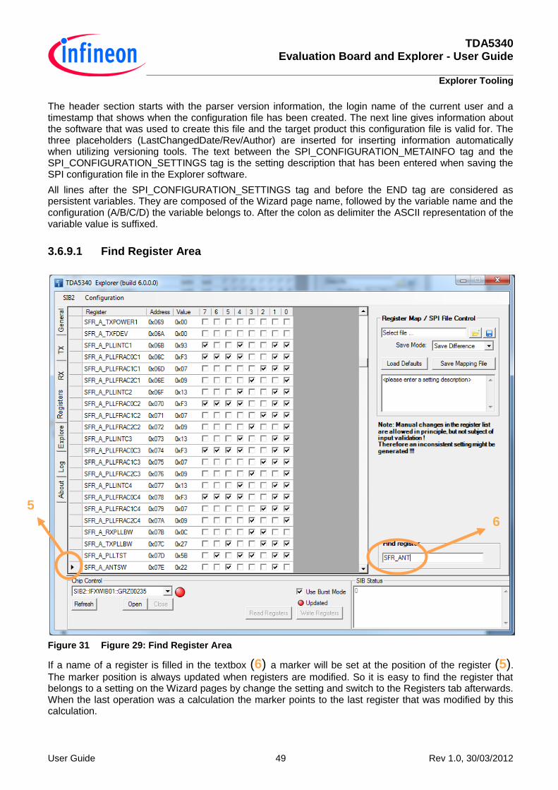
3.6.9.1 Find Register Area
Figure 31 Figure 29: Find Register Area
If a name of a register is filled in the textbox (6) a marker will be set at the position of the register (5).
The marker position is always updated when registers are modified. So it is easy to find the register that belongs to a setting on the Wizard pages by change the setting and switch to the Registers tab afterwards. When the last operation was a calculation the marker points to the last register that was modified by this calculation.
5
6

TDA5340 Evaluation Board and Explorer - User Guide
Explorer Tooling
User Guide 50 Rev 1.0, 30/03/2012
3.7 Register patch list
The following register values are written down from the Explorer Tooling to equalize the Explorer default setting and the TDA5340 SFR register list.
SFR_A_CDRCFG0 0x048 0x8C
SFR_B_CDRCFG0 0x148 0x8C
SFR_C_CDRCFG0 0x248 0x8C
SFR_D_CDRCFG0 0x348 0x8C
SFR_A_TSILENA 0x04E 0x01
SFR_B_TSILENA 0x14E 0x01
SFR_C_TSILENA 0x24E 0x01
SFR_D_TSILENA 0x34E 0x01
SFR_A_SYSRCTO 0x026 0x7C
SFR_B_SYSRCTO 0x126 0x7C
SFR_C_SYSRCTO 0x226 0x7C
SFR_D_SYSRCTO 0x326 0x7C
SFR_A_PDECF 0x03D 0x10
SFR_A_PDECSCFSK 0x03E 0x2A
SFR_A_PDECSCASK 0x03F 0x28
SFR_A_SRC 0x040 0x02
SFR_A_EXTSLC0 0x041 0x0B
SFR_B_PDECF 0x13D 0x10
SFR_B_PDECSCFSK 0x13E 0x2A
SFR_B_PDECSCASK 0x13F 0x28
SFR_B_SRC 0x140 0x02
SFR_B_EXTSLC0 0x141 0x0B
SFR_C_PDECF 0x23D 0x10
SFR_C_PDECSCFSK 0x23E 0x2A
SFR_C_PDECSCASK 0x23F 0x28
SFR_C_SRC 0x240 0x02
SFR_C_EXTSLC0 0x241 0x0B
SFR_D_PDECF 0x33D 0x10
SFR_D_PDECSCFSK 0x33E 0x2A
SFR_D_PDECSCASK 0x33F 0x28
SFR_D_SRC 0x340 0x02
SFR_D_EXTSLC0 0x341 0x0B
SFR_A_AFCKCFG0 0x033 0x50
SFR_B_AFCKCFG0 0x133 0x50
SFR_C_AFCKCFG0 0x233 0x50
SFR_D_AFCKCFG0 0x333 0x50
SFR_A_AFCKCFG1 0x034 0xC0
SFR_B_AFCKCFG1 0x134 0xC0
SFR_C_AFCKCFG1 0x234 0xC0
SFR_D_AFCKCFG1 0x334 0xC0
SFR_TXFIFOAEL 0x0CF 0x28
SFR_TXFIFOAFL 0x0D0 0x0A
SFR_IM2 0x0B9 0x20

TDA5340 Evaluation Board and Explorer - User Guide
Explorer Tooling
User Guide 51 Rev 1.0, 30/03/2012
3.8 Logging
Figure 32 Figure 30: Logging
Logging information and warnings are displayed here. Use the context menu of the NextGen Repository item in the tree view to change the warning-level.

w w w . i n f i n e o n . c o m
Published by Infineon Technologies AG