Small Signal Model • Bias Circuits • Field Effect ... · PDF file• Field Effect...
16
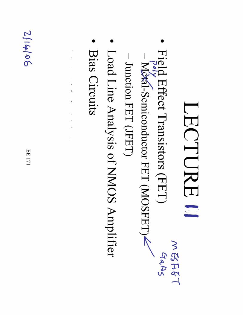
Feb 3, 2005 EE 171 LECTURE 8 • Field Effect Transistors (FET) – Metal-Semiconductor FET (MOSFET) – Junction FET (JFET) • Load Line Analysis of NMOS Amplifier • Bias Circuits • Small Signal Model
-
Upload
duongduong -
Category
Documents
-
view
219 -
download
2
Transcript of Small Signal Model • Bias Circuits • Field Effect ... · PDF file• Field Effect...
Feb 3,2005EE 171
LECTU
RE 8
•Field Effect Transistors (FET)–
Metal-Sem
iconductor FET (MO
SFET)–
Junction FET (JFET)•
Load Line Analysis of N
MO
S Am
plifier•
Bias C
ircuits•
Small Signal M
odel
Feb 3,2005EE 171
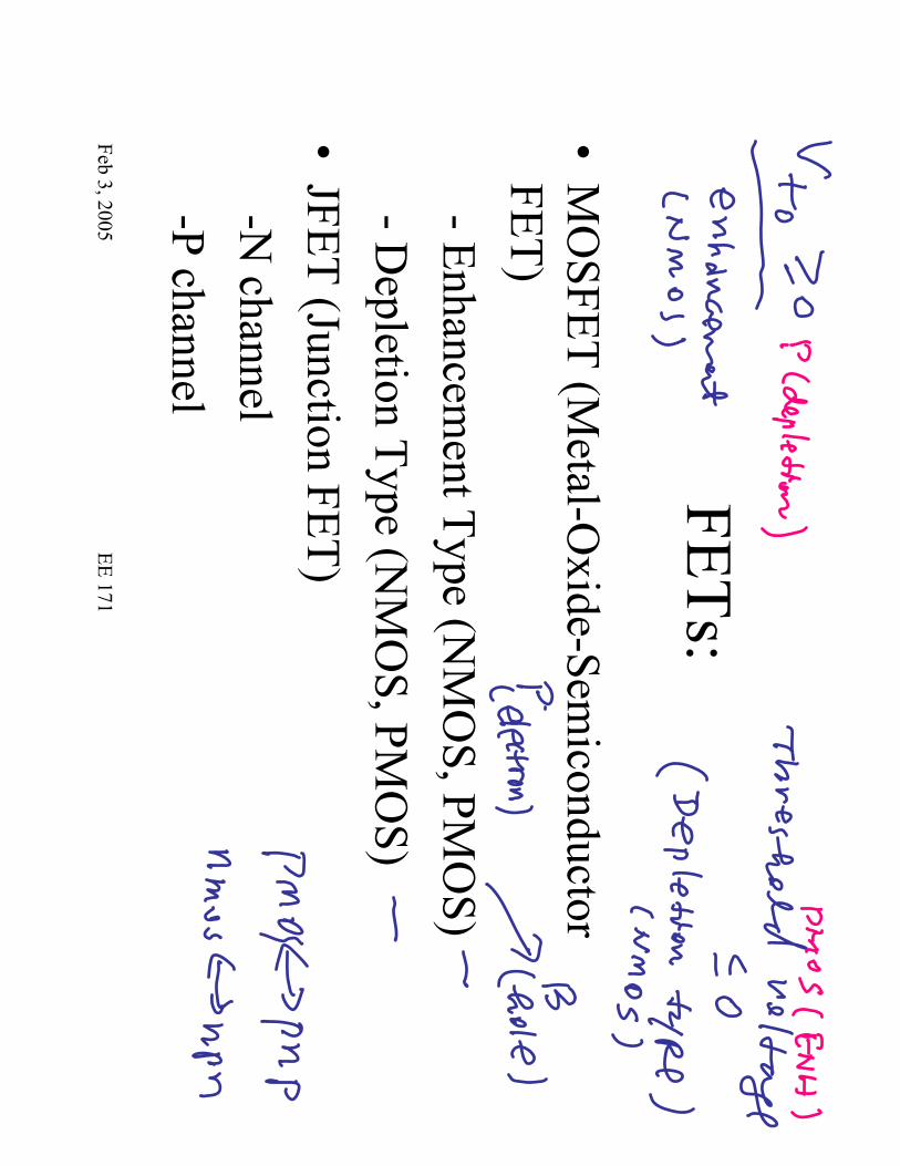
FETs:
•M
OSFET (M
etal-Oxide-Sem
iconductor FET)
-Enhancement Type (N
MO
S, PMO
S)-D
epletion Type (NM
OS, PM
OS)
•JFET (Junction FET)
-N channel
-P channel
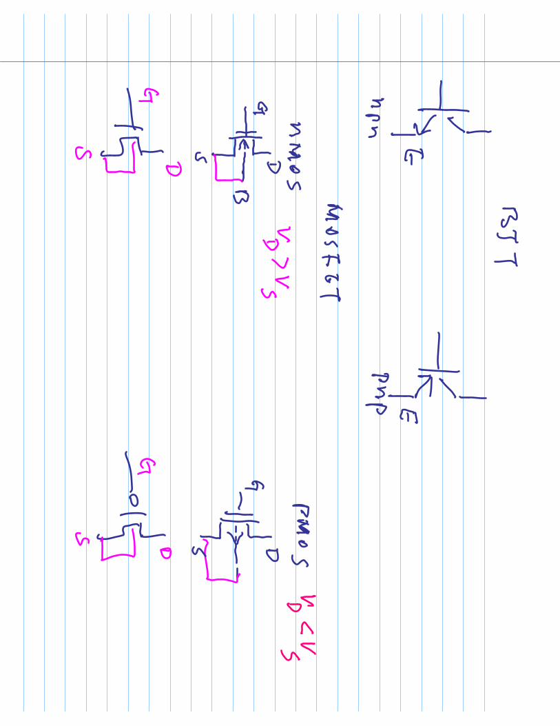
Feb 3,2005EE 171
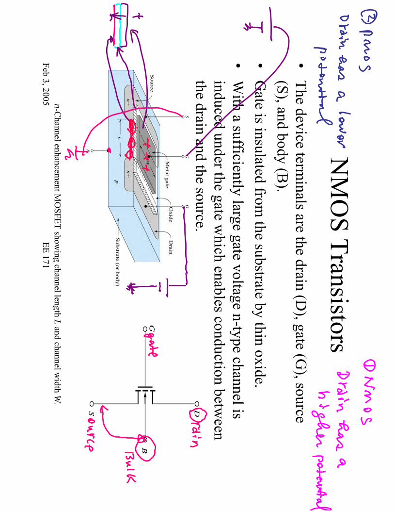
n-Channel enhancem
ent MO
SFET showing channel length L
and channel width W
.
NM
OS Transistors
•The device term
inals are the drain (D), gate (G
), source (S), and body (B
).•
Gate is insulated from
the substrate by thin oxide.•
With a sufficiently large gate voltage n-type channel is
induced under the gate which enables conduction betw
een the drain and the source.
Feb 3,2005EE 171
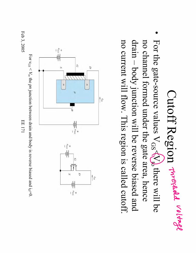
For vG
S < Vto the pn
junction between drain and body is reverse biased and iD =0.
Cutoff R
egion•
For the gate-source values VG
S <Vto there w
ill be no channel form
ed under the gate area, hence drain –
body junction will be reverse biased and
no current will flow
. This region is called cutoff.
Feb 3,2005EE 171
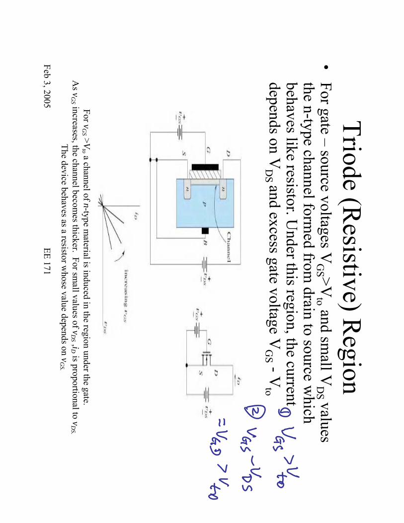
For vG
S >Vto a channel of n-type m
aterial is induced in the region under the gate. A
s vG
S increases, the channel becomes thicker. For sm
all values of vD
S ,iDis proportional to v
DS.
The device behaves as a resistor whose value depends on v
GS.
Triode (Resistive) R
egion•
For gate –source voltages V
GS >V
to and small V
DS values
the n-type channel formed from
drain to source which
behaves like resistor. Under this region, the current
depends on VD
S and excess gate voltage VG
S -Vto
Feb 3,2005EE 171
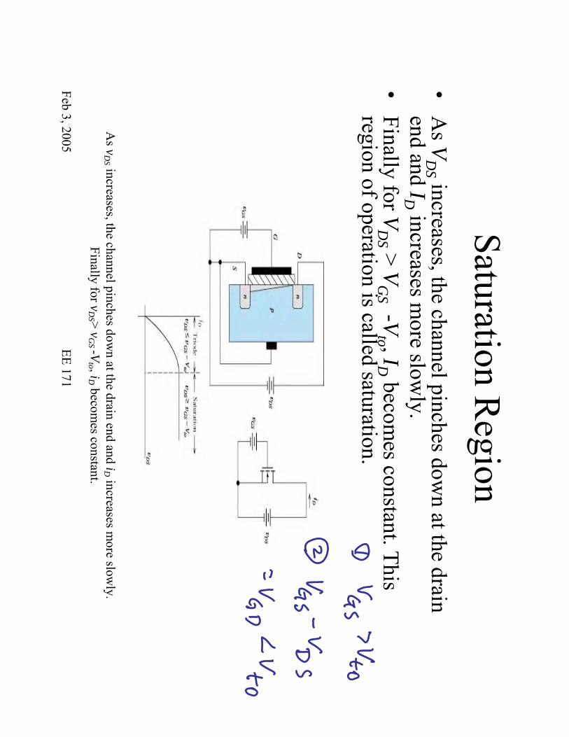
As v
DS increases, the channel pinches dow
n at the drain end and iDincreases m
ore slowly.
Finally for vD
S > vG
S -Vto , iD
becomes constant.
Saturation Region
•A
s VD
S increases, the channel pinches down at the drain
end and IDincreases m
ore slowly.
•Finally for V
DS > V
GS
-Vto , ID
becomes constant. This
region of operation is called saturation.
Feb 3,2005EE 171
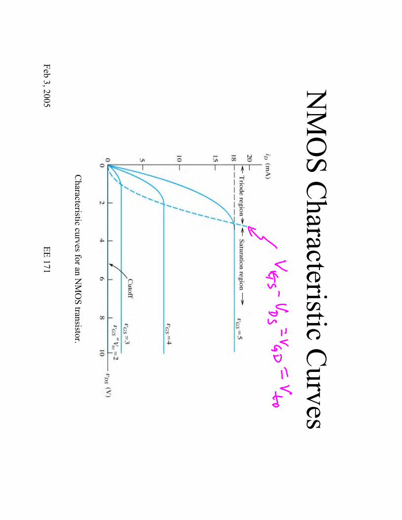
Characteristic curves for an N
MO
S transistor.
NM
OS C
haracteristic Curves
Feb 3,2005EE 171
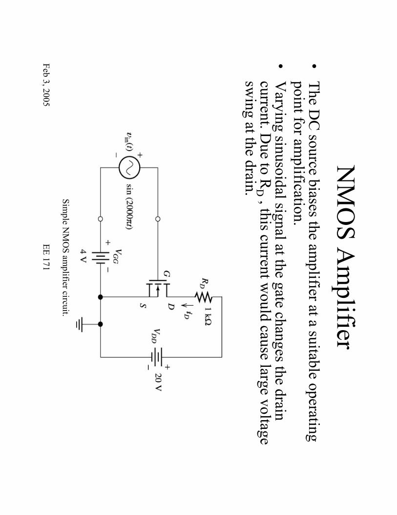
Simple N
MO
S amplifier circuit.
NM
OS A
mplifier
•The D
C source biases the am
plifier at a suitable operating point for am
plification.•
Varying sinusoidal signal at the gate changes the drain
current. Due to R
D, this current w
ould cause large voltage sw
ing at the drain.
Feb 3,2005EE 171
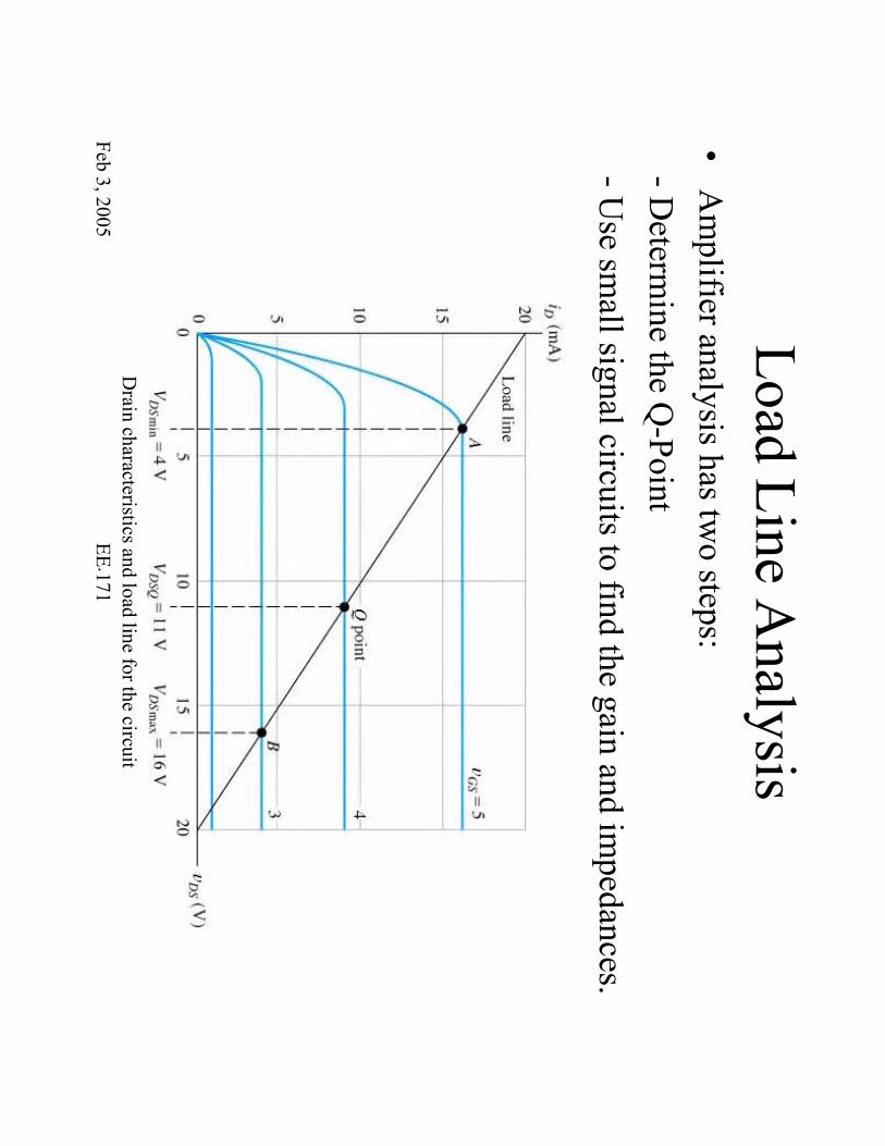
Drain characteristics and load line for the circuit
.
Load Line Analysis
•A
mplifier analysis has tw
o steps:-D
etermine the Q
-Point-U
se small signal circuits to find the gain and im
pedances.

Feb 3,2005EE 171
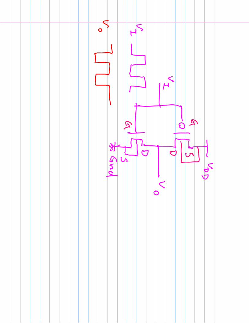
Fixed-plus self-bias circuit.
Biasing
•Fixed-plus self-bias is generally applied to establish Q
-points that are relatively independent of device param
eters.
Feb 3,2005EE 171
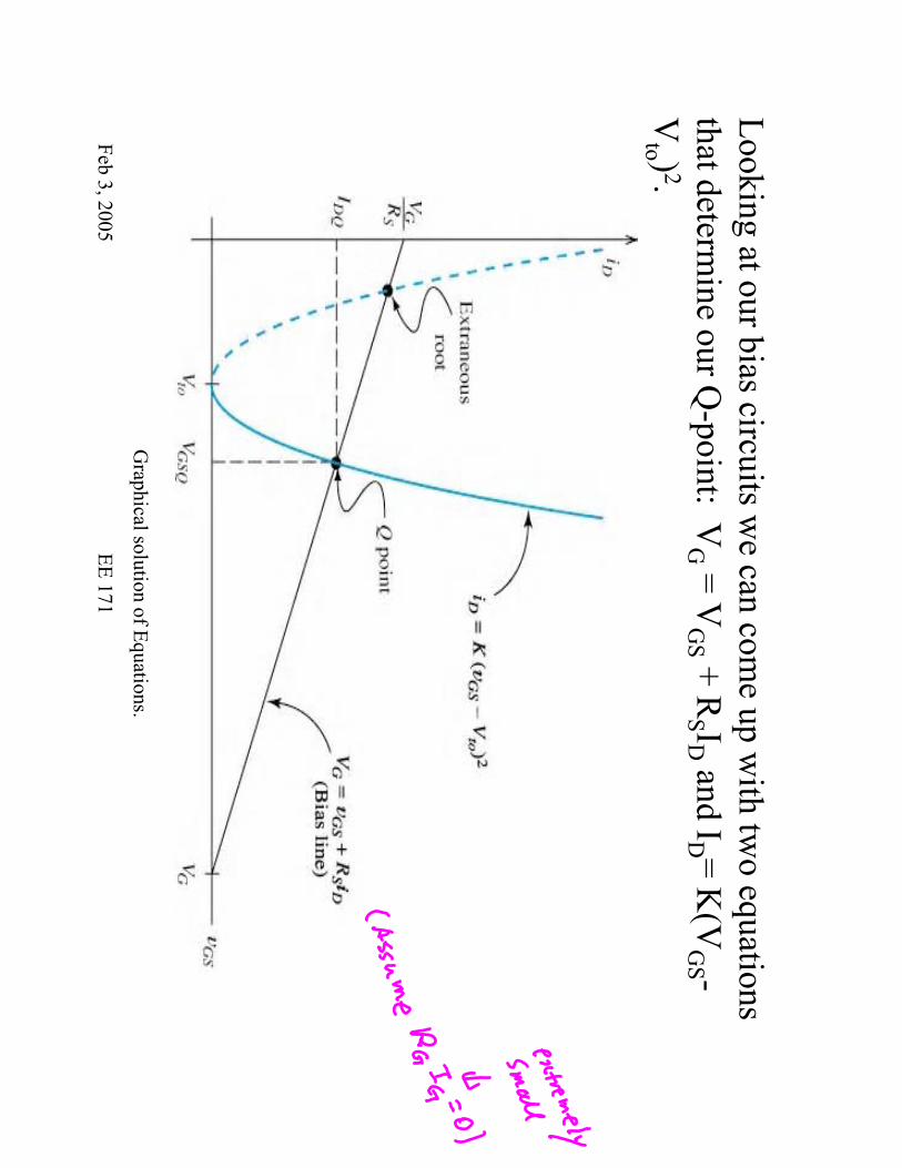
Graphical solution of Equations.
Looking at our bias circuits we can com
e up with tw
o equations that determ
ine our Q-point: V
G= V
GS + R
S IDand ID = K
(VG
S -V
to ) 2.
Feb 3,2005EE 171
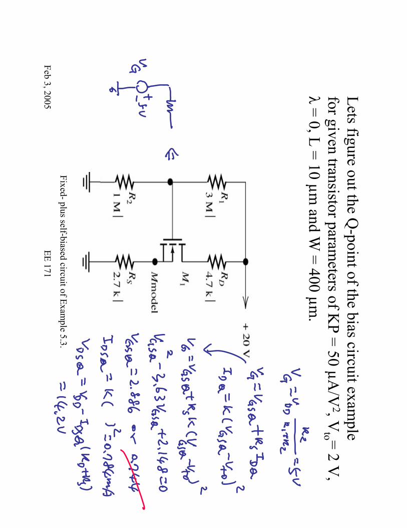
Fixed-plus self-biased circuit of Example 5.3.
Lets figure out the Q-point of the bias circuit exam
ple for given transistor param
eters of KP = 50 µA
/V2, V
to = 2 V,
λ= 0, L = 10 µm
and W = 400 µm
.
Feb 3,2005EE 171
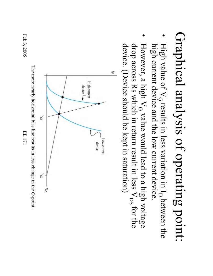
The more nearly horizontal bias line results in less change in the Q
-point.
Graphical analysis of operating point:
•H
igh value of VG
results in less variation in ID betw
een the high current device and the low
current device.•
How
ever, a high VG
value would lead to a high voltage
drop across Rsw
hich in return result in less VD
S for the device. (D
evice should be kept in saturation)