Small PIM module (M728/M732) Evaluation Board · Supported modules : Small PIM (M728/M732) solder...
24
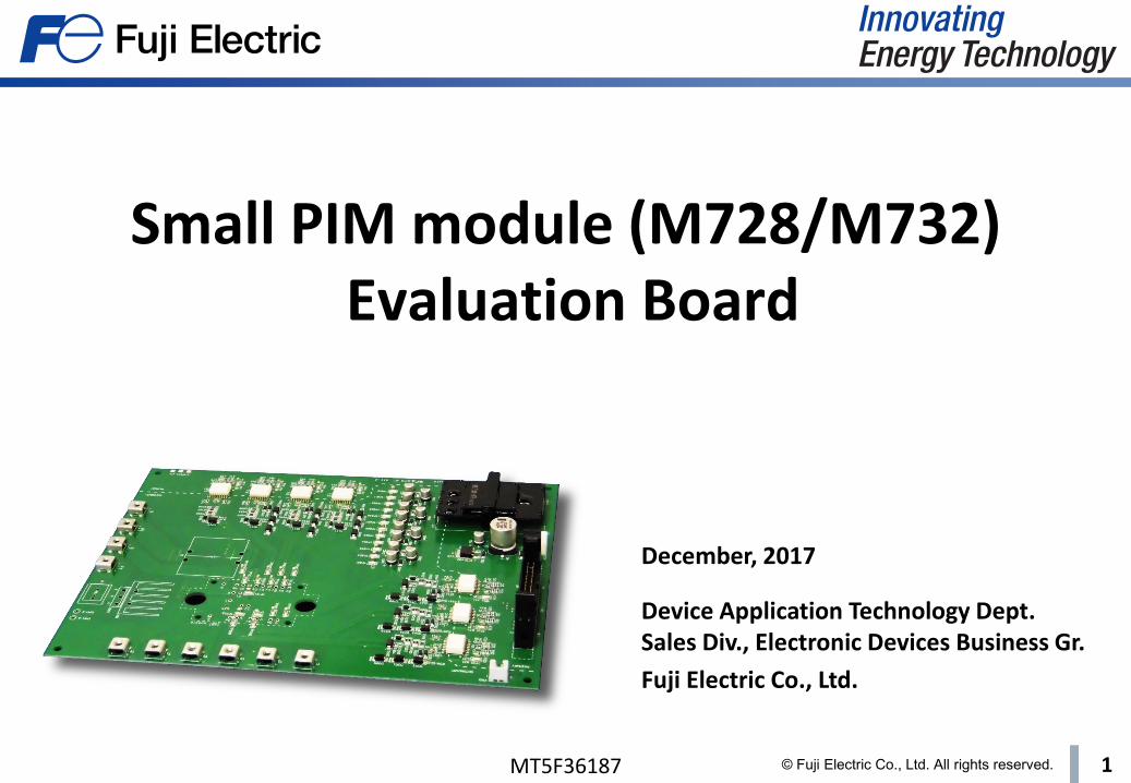
© Fuji Electric Co., Ltd. All rights reserved. 1 Small PIM module (M728/M732) Evaluation Board Device Application Technology Dept. Sales Div., Electronic Devices Business Gr. Fuji Electric Co., Ltd. December, 2017 MT5F36187
Transcript of Small PIM module (M728/M732) Evaluation Board · Supported modules : Small PIM (M728/M732) solder...
© Fuji Electric Co., Ltd. All rights reserved. 1
Small PIM module (M728/M732)Evaluation Board
Device Application Technology Dept.Sales Div., Electronic Devices Business Gr.
Fuji Electric Co., Ltd.
December, 2017
MT5F36187
© Fuji Electric Co., Ltd. All rights reserved. 2
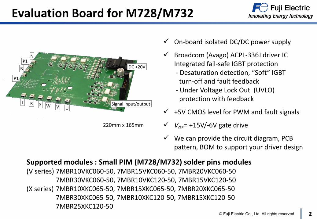
Evaluation Board for M728/M732
On-board isolated DC/DC power supply
Broadcom (Avago) ACPL-336J driver ICIntegrated fail-safe IGBT protection- Desaturation detection, “Soft” IGBT
turn-off and fault feedback- Under Voltage Lock Out (UVLO)
protection with feedback
+5V CMOS level for PWM and fault signals
VGE= +15V/-6V gate drive
We can provide the circuit diagram, PCBpattern, BOM to support your driver design
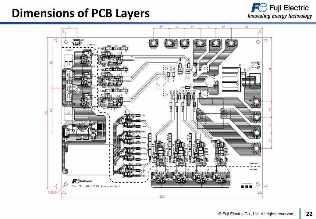
220mm x 165mm
Supported modules : Small PIM (M728/M732) solder pins modules(V series) 7MBR10VKC060-50, 7MBR15VKC060-50, 7MBR20VKC060-50
7MBR30VKC060-50, 7MBR10VKC120-50, 7MBR15VKC120-50(X series) 7MBR10XKC065-50, 7MBR15XKC065-50, 7MBR20XKC065-50
7MBR30XKC065-50, 7MBR10XKC120-50, 7MBR15XKC120-507MBR25XKC120-50
Signal Input/output
DC +20V
R STUVW
P1
B
P1N

© Fuji Electric Co., Ltd. All rights reserved. 3
Layout of the Evaluation Board
IC8: DC/DC power supply
IC1 – IC7: Gate driver ICACPL-336J
CN1: Power supply connector(DC +20V)
CN2: Gate PWM signal input/Fault signal output
CN3: NTC output
T1 – T3: 3φ AC output terminal
T4 – T6: 3φ AC input terminal
T7,T9: DC+ terminal
T10: DC- terminal
T8: Brake terminal
(P1) T9
Z Y XDB IC8(MS57140-07)
CN3
CN2
U
V
W
CN1
IC3 – IC9(ACPL-336J x7)
(B) T8
(P1) T7
T6(T)
T4(R)
T5(S)
T3(W)
T2(V)
T1(U)
(N) T10

© Fuji Electric Co., Ltd. All rights reserved. 4
Assembling
(2) Attach and solder IGBT module to PCB
(3) Connect I/O signal and DC power supply
IC8(M57140-07F)
(1) Attach IC8 (M57140-07F)
CN8: I/O signalCN1: 20V (DC)
For reverse bias less voltage supply use M57140-01F
© Fuji Electric Co., Ltd. All rights reserved. 5
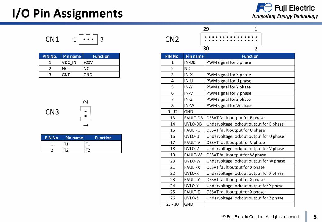
I/O Pin Assignments
CN2CN1
CN3
PIN No. Pin name Function
1 IN-DB PWM signal for B phase
2 NC
3 IN-X PWM signal for X phase
4 IN-U PWM signal for U phase
5 IN-Y PWM signal for Y phase
6 IN-V PWM signal for V phase
7 IN-Z PWM signal for Z phase
8 IN-W PWM signal for W phase
9 - 12 GND
13 FAULT-DB DESAT fault output for B phase
14 UVLO-DB Undervoltage lockout output for B phase
15 FAULT-U DESAT fault output for U phase
16 UVLO-U Undervoltage lockout output for U phase
17 FAULT-V DESAT fault output for V phase
18 UVLO-V Undervoltage lockout output for V phase
19 FAULT-W DESAT fault output for W phase
20 UVLO-W Undervoltage lockout output for W phase
21 FAULT-X DESAT fault output for X phase
22 UVLO-X Undervoltage lockout output for X phase
23 FAULT-Y DESAT fault output for X phase
24 UVLO-Y Undervoltage lockout output for Y phase
25 FAULT-Z DESAT fault output for X phase
26 UVLO-Z Undervoltage lockout output for Z phase
27 - 30 GND
PIN No. Pin name Function
1 VDC_IN +20V
2 NC NC
3 GND GND
PIN No. Pin name Function
1 T1 T1
2 T2 T2
3

© Fuji Electric Co., Ltd. All rights reserved. 6
Description Parameter Value Unit Remarks
DC input voltage for DC/DC converter V DC(in) 18 ~ 22 V Recommended value: 20V
DC output votlage of DC/DC converter V out1 +15/-6 V Gate-Emitter voltage
Primary side control voltage V out2 5 V Non-isolation
PWM singal input voltage V IN 0 / +5 V
Peak output current I O(peak) 2.5 A Follow the specification of ACPL-336J
Peak output current for gate drive per IGBT I O(peak) 2.5 A Follow the specification of ACPL-336J
Operating temperature T opr -10... +75 oC
Storage temperature T stg -20... +85 oC
FAULT output current I FAULT 10 mA Follow the specification of ACPL-336J
FAULT pin voltage V FAULT 5 V Follow the specification of ACPL-336J
FAULT logic low output current I FAULT_L 9.0 mA Follow the specification of ACPL-336J
UVLO output current I UVLO 10 mA Follow the specification of ACPL-336J
UVLO pin voltage V UVLO 5 V Follow the specification of ACPL-336J
UVLO threshould low to high V UVLO+ 12.5 V Follow the specification of ACPL-336J
UVLO threshould high to low V UVLO- 11.3 V Follow the specification of ACPL-336J
DESAT detection threshold V DESAT 7 V Follow the specification of ACPL-336J
Output Mute Time due to DESAT t DESAT(MUTE) 3.0 ms Follow the specification of ACPL-336J
Time Input Kept Low Before Fault Reset to High t DESAT(RESET) 3.0 ms Follow the specification of ACPL-336J
Electrical Characteristics
Please refer to datasheet of ACPL-336J and M57140-07F for other characteristics.

© Fuji Electric Co., Ltd. All rights reserved. 7
Example of Switching Waveform
Turn on Turn off Reverse Recovery
VGE (10V/div)
VCE (200V/div)
IC (10A/div)
t: 200ns/div
VAK(200V/div)
IF (10A/div)
VGE (10V/div)
VCE (200V/div)
IC (10A/div)
t: 200ns/div t: 100ns/div
Test condition:Module: 7MBR15VKC120-50Vcc=600V, IC, IF=30A, RG=39Ω, VGE=+15V/-6V, Tvj=R.T.
The initial value of RG is 15Ω.Before measurement, please decide RG value of test module by specification.

© Fuji Electric Co., Ltd. All rights reserved. 8
Short Circuit Protection (DESAT)
FAULT
IC (50A/div)
Short circuit waveforms FAULT signal output
Short circuit
Test condition:Module: 7MBR15VKC120-50Vcc=800V, RG=39Ω, VGE=+15V/-6V, Tvj=R.T.
6.4ms
VGE (10V/div)
VCE (200V/div)
IC (25A/div)
Vin
t: 1µs/div t: 2ms/div
© Fuji Electric Co., Ltd. All rights reserved. 9
Circuit Diagram (Main Circuit)
G(U) G(V) G(W)
G(X) G(Y) G(Z)G(DB)
T4
T5
T6
T8
T9
T10
T1
T2
T3
R
S
T
U
V
W
B P1
P1
N
IGBTmodule
C1
CN3
E(N)
E(U) E(V) E(W)
U
V
W
R
S
T
N Gb Nb Gx Gy Gz Ez
UVW
GwWGvVGuUB P1P
T1T2
T7
Ex Ey
THY1-G THY1-K
R1
THY1
P1
© Fuji Electric Co., Ltd. All rights reserved. 10
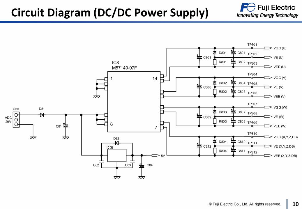
Circuit Diagram (DC/DC Power Supply)
IC8M57140-07F
IC9
D81
C81
D82
C82 C83 C84
5V
C801
C802
C804
C805
C807
C808
C810
C811
C803
C806
C809
C812
D801
D802
D803
D804
R801
R802
R803
R804
VDC
20V
CN1
TP801
TP802
TP803
TP804
TP805
TP806
TP807
TP808
TP809
TP810
TP811
TP812
1
6
14
7
VGG (X,Y,Z,DB)
VE (X,Y,Z,DB)
VEE (X,Y,Z,DB)
VGG (U)
VE (U)
VEE (U)
VGG (V)
VE (V)
VEE (V)
VGG (W)
VE (W)
VEE (W)
© Fuji Electric Co., Ltd. All rights reserved. 11
Circuit Diagram (Gate Drive) (1/2)
VEE1
VIN +
VCC1
VLEDDRV
UVL O
VEE2
VLED
DESAT
VE
VCC2
VO UT
VCLAM P
VEE2
FA ULT
AN ODE
CATHOD E
5V
VGG(U)
VEE(U)
IN-U
UVLO-U
FAULT-U
P1
G(U)
IC1C11
R12 R13
R15
R14C13C12
D103 D104 D105
R103
R102
R11
VE(U)
E(U)
D106
D101 D102
R101R104
C101
C102
C103
C104
C105 D107
D108
TP101
TP102
TP103
TP11
VEE1
VIN +
VCC1
VLEDDRV
UVL O
VEE2
VLED
DESAT
VE
VCC2
VO UT
VCLAM P
VEE2
FA ULT
AN ODE
CATHOD E
5V
VGG(W)
VEE(W)
IN-W
UVLO-W
FAULT-W
P1
G(W)
IC3C31
R32 R33
R35
R34C33C32
D303 D304 D305
R303
R302
R31
VE(W)
E(W)
D306
D301 D302
R301R304
C301
C302
C303
C304
C305 D307
D308
TP302
TP303
TP31
VEE1
VIN +
VCC1
VLEDDRV
UVL O
VEE2
VLED
DESAT
VE
VCC2
VO UT
VCLAM P
VEE2
FA ULT
AN ODE
CATHOD E
5V
VGG(V)
VEE(V)
IN-V
UVLO-V
FAULT-V
P1
G(V)
IC2C21
R22 R23
R25
R24C23C22
D203 D204 D205
R203
R202
R21
VE(V)
E(V)
D206
D201 D202
R201R204
C201
C202
C203
C204
C205 D207
D208
TP202
TP203
TP21
IN-DB
IN-Z
IN-Y
IN-X
IN-W
IN-V
IN-U
UVLO-U
UVLO-V
UVLO-DB
UVLO-W
UVLO-X
UVLO-Y
UVLO-ZFAULT-Z
FAULT-X
FAULT-Y
FAULT-DB
FAULT-WFAULT-V
FAULT-U
CN2
NC

© Fuji Electric Co., Ltd. All rights reserved. 12
Circuit Diagram (Gate Drive) (2/2)
VE E1
VIN+
VCC1
VLEDDRV
UVL O
VEE2
VLED
DESAT
VE
VCC2
VO UT
VCLAM P
VEE2
FA ULT
AN ODE
CATHOD E
5V
VGG(X,Y,Z,DB)
VEE(X,Y,Z,DB)
IN-X
UVLO-X
FAULT-X
U
G(X)
IC4C41
R42 R43
R45
R44C43C42
D403 D404 D405
R403
R402
R41
VE(X,Y,Z,DB)
E(N)
D406
D401 D402
R401R404
C401
C402
C403
C404
C405 D407
D408
TP402
TP403
TP41
VE E1
VIN+
VCC1
VLEDDRV
UVL O
VEE2
VLED
DESAT
VE
VCC2
VO UT
VCLAM P
VEE2
FA ULT
AN ODE
CATHOD E
5V
VGG(X,Y,Z,DB)
VEE(X,Y,Z,DB)
IN-Y
UVLO-Y
FAULT-Y
V
G(Y)
IC5C51
R52 R53
R55
R54C53C52
D503 D504 D505
R503
R502
R51
VE(X,Y,Z,DB)
E(N)
D506
D501 D502
R501R504
C501
C502
C503
C504
C505 D507
D508
TP502
TP503
TP51
VE E1
VIN +
VCC1
VLEDDRV
UVL O
VEE2
VLED
DESAT
VE
VCC2
VO UT
VCLAM P
VEE2
FA ULT
AN ODE
CATHOD E
5V
VGG(X,Y,Z,DB)
VEE(X,Y,Z,DB)
IN-Z
UVLO-Z
FAULT-Z
W
G(Z)
IC6C61
R62 R63
R65
R64C63C62
D603 D604 D605
R603
R602
R61
VE(X,Y,Z,DB)
E(N)
D606
D601 D602
R601R604
C601
C602
C603
C604
C605 D607
D608
TP602
TP603
TP61
VE E1
VIN +
VCC1
VLEDDRV
UVL O
VEE2
VLED
DESAT
VE
VCC2
VO UT
VCLAM P
VEE2
FA ULT
AN ODE
CATHOD E
5V
VGG(X,Y,Z,DB)
VEE(X,Y,Z,DB)
IN-DB
UVLO-DB
FAULT-DB G(DB)
IC7C71
R72 R73
R75
R74C73C72
R703
R702
R71
VE(X,Y,Z,DB)
E(N)
D706
R704
C701
C703
C704
C705 D707
D708
TP702
TP703
TP71
© Fuji Electric Co., Ltd. All rights reserved. 13
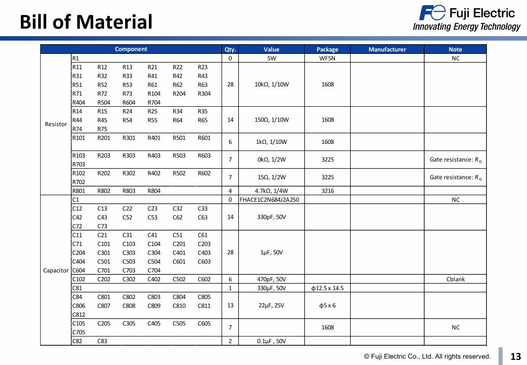
Bill of MaterialQty. Value Package Manufacturer Note
R1 0 5W WF5N NC
R11 R12 R13 R21 R22 R23
R31 R32 R33 R41 R42 R43
R51 R52 R53 R61 R62 R63
R71 R72 R73 R104 R204 R304
R404 R504 R604 R704
R14 R15 R24 R25 R34 R35
R44 R45 R54 R55 R64 R65
R74 R75
R101 R201 R301 R401 R501 R601
R103 R203 R303 R403 R503 R603
R703
R102 R202 R302 R402 R502 R602
R702
R801 R802 R803 R804 4 4.7kΩ, 1/4W 3216
C1 0 FHACE1C2N684J2A2S0 NC
C12 C13 C22 C23 C32 C33
C42 C43 C52 C53 C62 C63
C72 C73
C11 C21 C31 C41 C51 C61
C71 C101 C103 C104 C201 C203
C204 C301 C303 C304 C401 C403
C404 C501 C503 C504 C601 C603
C604 C701 C703 C704
C102 C202 C302 C402 C502 C602 6 470pF, 50V Cblank
C81 1 330μF, 50V φ12.5 x 14.5
C84 C801 C802 C803 C804 C805
C806 C807 C808 C809 C810 C811
C812
C105 C205 C305 C405 C505 C605
C705
C82 C83 2 0.1μF , 50V
14 150Ω, 1/10W 1608
6 1kΩ, 1/10W 1608
3225 Gate resistance: RG
Component
Resistor
28 10kΩ, 1/10W 1608
7 15Ω, 1/2W 3225 Gate resistance: RG
7 0kΩ, 1/2W
14 330pF, 50V
28 1μF, 50V
Capacitor
13 22μF, 25V φ5 x 6
7 1608 NC
© Fuji Electric Co., Ltd. All rights reserved. 14
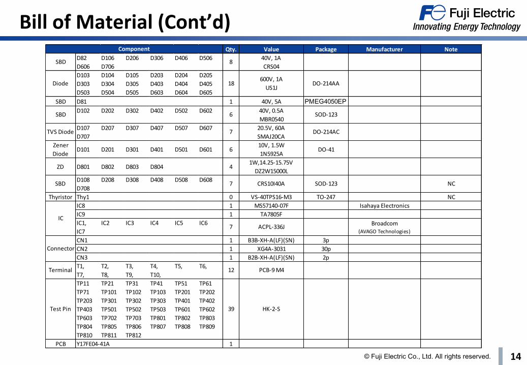
Bill of Material (Cont’d)Qty. Value Package Manufacturer Note
D82 D106 D206 D306 D406 D506
D606 D706
D103 D104 D105 D203 D204 D205
D303 D304 D305 D403 D404 D405
D503 D504 D505 D603 D604 D605
SBD D81 1 40V, 5A PMEG4050EP
D102 D202 D302 D402 D502 D602
D107 D207 D307 D407 D507 D607
D707
Zener
DiodeD101 D201 D301 D401 D501 D601 6
10V, 1.5W
1N5925ADO-41
ZD D801 D802 D803 D804 41W,14.25-15.75V
DZ2W15000L
D108 D208 D308 D408 D508 D608
D708
Thyristor Thy1 0 VS-40TPS16-M3 TO-247 NC
IC8 1 MS57140-07F Isahaya Electronics
IC9 1 TA7805F
IC1, IC2 IC3 IC4 IC5 IC6
IC7
CN1 1 B3B-XH-A(LF)(SN) 3p
CN2 1 XG4A-3031 30p
CN3 1 B2B-XH-A(LF)(SN) 2p
T1, T2, T3, T4, T5, T6,
T7, T8, T9, T10,
TP11 TP21 TP31 TP41 TP51 TP61
TP71 TP101 TP102 TP103 TP201 TP202
TP203 TP301 TP302 TP303 TP401 TP402
TP403 TP501 TP502 TP503 TP601 TP602
TP603 TP702 TP703 TP801 TP802 TP803
TP804 TP805 TP806 TP807 TP808 TP809
TP810 TP811 TP812
PCB 1
Component
SBD 840V, 1A
CRS04
SBD 640V, 0.5A
MBR0540SOD-123
Diode 18600V, 1A
US1JDO-214AA
TVS Diode 720.5V, 60A
SMAJ20CADO-214AC
SBD 7 CRS10I40A SOD-123 NC
IC
7 ACPL-336JBroadcom
(AVAGO Technologies)
Connector
Terminal 12 PCB-9 M4
Y17FE04-41A
Test Pin 39 HK-2-S

© Fuji Electric Co., Ltd. All rights reserved. 15
(Top Silkscreen Layer)
PCB Layers
© Fuji Electric Co., Ltd. All rights reserved. 16
PCB Layers
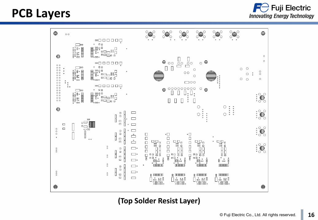
(Top Solder Resist Layer)
© Fuji Electric Co., Ltd. All rights reserved. 17
PCB Layers
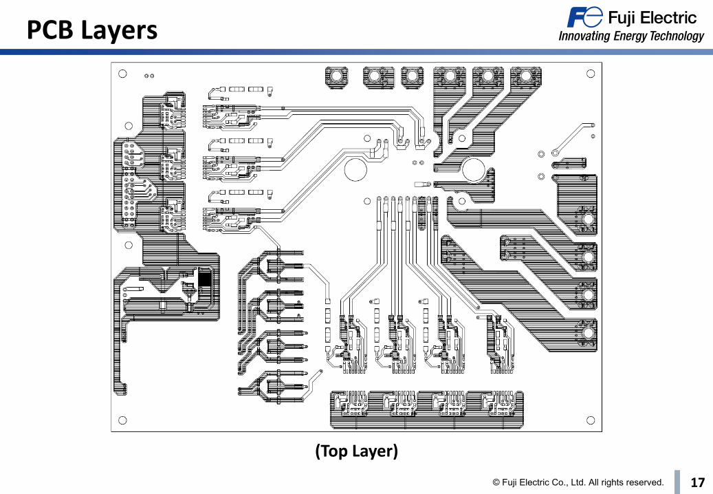
(Top Layer)

© Fuji Electric Co., Ltd. All rights reserved. 18
PCB Layers
(Layer 2)
© Fuji Electric Co., Ltd. All rights reserved. 19
PCB Layers
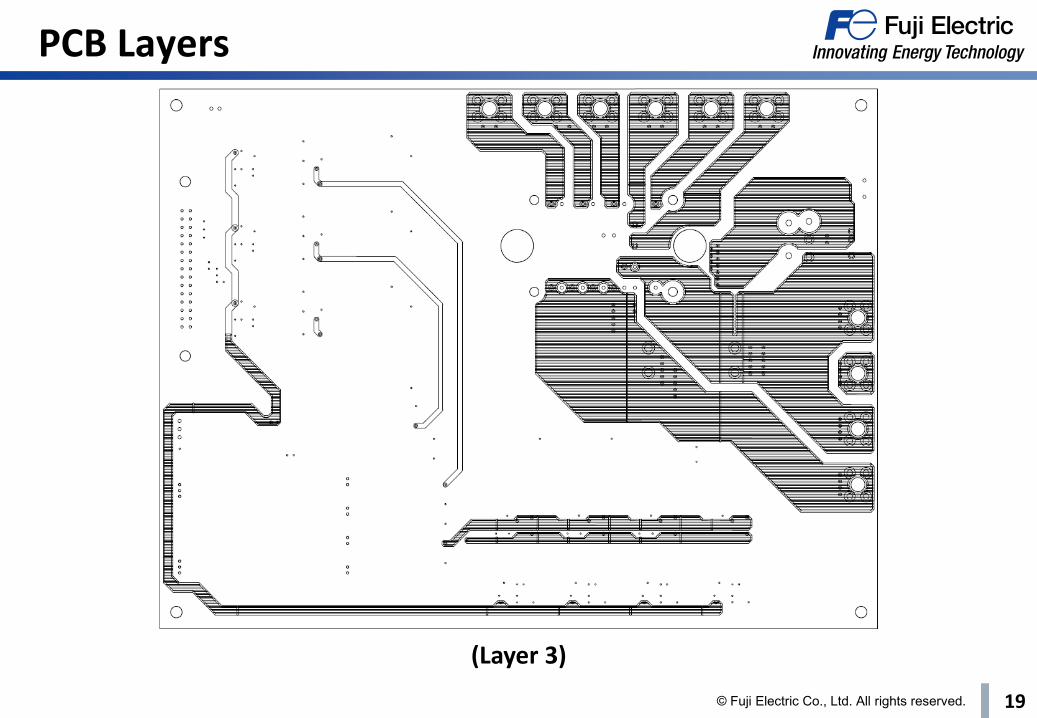
(Layer 3)

© Fuji Electric Co., Ltd. All rights reserved. 20
PCB Layers
(Bottom Layer)

© Fuji Electric Co., Ltd. All rights reserved. 21
PCB Layers
(Bottom Solder Resist Layer)
© Fuji Electric Co., Ltd. All rights reserved. 22
Dimensions of PCB Layers

© Fuji Electric Co., Ltd. All rights reserved. 23
Contact
CAD-data and gerber-data for this evaluation board are also available on request.
This evaluation board can be ordered via a representative at our company or one of our dealers.
If you don’t know the contact address, please request through our website:www.fujielectric.com/products/semiconductor/contact/
For more information, please visit our website: www.fujielectric.com/products/semiconductor/

© Fuji Electric Co., Ltd. All rights reserved. 24
Warnings
1. This Catalog contains the product specifications, characteristics, data, materials, and structures as of December 2017. The contents are subject to change without notice for specification changes or other reason. When using a product listed in this Catalog, be sure to obtain the latest specifications.
2. All applications described in this Catalog exemplify the use of Fuji’s products for your reference only. No right or license, either express or implied, under any patent, copyright, trade secret or other intellectual property right owned by Fuji Electric Co., Ltd. is (or shall be deemed) granted. Fuji Electric Co., Ltd. makes no representation or warranty, whether express or implied, relating to the infringement or alleged infringement of other’s intellectual property rights which may arise from the use of the applications described herein.
3. Although Fuji Electric Co., Ltd. is enhancing product quality and reliability, a small percentage of semiconductor products may become faulty. When using Fuji Electric semiconductor products in your equipment, you are requested to take adequate safety to prevent the equipment from causing a physical injury, fire, or other problem if any of the products become faulty. It is recommended to make your design failsafe, flame retardant, and free of malfunction.
4. The products introduced in this Catalog are intended for use in the following electronic and electrical equipment which has normal reliability requirements.- Computers - OA equipment - Communications equipment (terminal devices) - Measurement equipment- Machine tools - Audiovisual equipment - Electrical home appliances - Personal equipment - Industrial robots etc.
5. If you need to use a product in this Catalog for equipment requiring higher reliability than normal, such as for the equipment listed below, it is imperative to contact Fuji Electric Co., Ltd. to obtain prior approval. When using these products for such equipment, take adequate measures such as a backup system to prevent the equipment from malfunctioning even if a Fuji’s product incorporated in the equipment becomes faulty.- Transportation equipment (mounted on cars and ships) - Trunk communications equipment -Traffic-signal control equipment- Gas leakage detectors with an auto-shut-off feature - Emergency equipment for responding to disasters and anti-burglary devices- Safety devices - Medical equipment.
6. Do not use products in this Catalog for the equipment requiring strict reliability such as the following and equivalents to strategic equipment (without limitation).- Space equipment - Aeronautic equipment - Nuclear control equipment - Submarine repeater equipment
7. All rights reserved. No part of this Catalog may be reproduced without permission in writing from Fuji Electric Co., Ltd.8. If you have any question about any portion in this Catalog, ask Fuji Electric Co., Ltd. or its sales agents before using the product. Neither Fuji Electric
Co., Ltd. nor its agents shall be liable for any injury caused by any use of the products not in accordance with instructions set forth herein.