Small and Wideband Patch Antennas and Planar … research 201601… · Small and Wideband Patch...
83
11/1/2016 1 Small and Wideband Patch Antennas and Planar Microwave Circuits for Wireless and Biomedical Applications Dr. Yongxin Guo, Associate Professor Department of Electrical and Computer Engineering Email: [email protected] 11 January 2016 1 Copyright © Dr. Yongxin Guo Abstract/Keywords Copyright © Dr. Yongxin Guo Abstract: In this presentation, the recent research activities on “Small and Wideband Patch Antennas and Planar Microwave Circuits for Wireless and Biomedical Applications” conducted by the research group led by Associate Professor Yongxin Guo at the Department of Electrical and Computer Engineering, National University of Singapore will be reported. The topics on “Antennas and Wireless Power for Biomedical Applications” has received a lot of attention. On- body antennas for wearable applications and In-body antennas for bio-implants will be presented first. Wireless power and energy harvesting have become more important to enable bio-telemetry. In addition to the traditional inductive near-field wireless power, capacitive wireless power and far-field wireless power will also be addressed. In the meantime, effort has been made to improve the dynamic range of the rectifier circuit for the energy harvesting, especially for low-power scenarios. The topic on “Small and Wideband Patch Antennas” has been focused previously. The wideband L-probe feeding technique will be introduced here. In the meantime, wideband patch antennas with broadband feeding networks will be presented. The antenna performance can be improved significantly in a wide bandwidth with the proposed broadband feeding networks. Various wideband millimeter-wave antennas-in-package and on-chip antennas will also be reported for future system in package applications since antennas are small in size at higher frequencies. “MMIC modeling and design” is another topic we are put effort on as it is crucial to develop high-density integrated transceivers for wireless and biomedical applications. It is believed that developing high-density integrated transceiver technologies for wireless and biomedical applications will attract more interests. Keywords: Wideband patch antennas, small antennas, wearable antennas, implantable antennas, antennas in package, on-chip antennas, wideband feeding networks, wireless power, inductive wireless power, capacitive wireless power, far-field wireless power, RF energy harvesting, MMIC, LTCC.
Transcript of Small and Wideband Patch Antennas and Planar … research 201601… · Small and Wideband Patch...
11/1/2016
1
Small and Wideband Patch Antennas and Planar Microwave Circuits for
Wireless and Biomedical Applications
Dr. Yongxin Guo, Associate ProfessorDepartment of Electrical and Computer Engineering
Email: [email protected] January 2016
1Copyright © Dr. Yongxin Guo
Abstract/Keywords
Copyright © Dr. Yongxin Guo
Abstract: In this presentation, the recent research activities on “Small and Wideband Patch Antennas and PlanarMicrowave Circuits for Wireless and Biomedical Applications” conducted by the research group led byAssociate Professor Yongxin Guo at the Department of Electrical and Computer Engineering, National University ofSingapore will be reported.
The topics on “Antennas and Wireless Power for Biomedical Applications” has received a lot of attention. On-body antennas for wearable applications and In-body antennas for bio-implants will be presented first. Wirelesspower and energy harvesting have become more important to enable bio-telemetry. In addition to the traditionalinductive near-field wireless power, capacitive wireless power and far-field wireless power will also be addressed. Inthe meantime, effort has been made to improve the dynamic range of the rectifier circuit for the energy harvesting,especially for low-power scenarios.
The topic on “Small and Wideband Patch Antennas” has been focused previously. The wideband L-probe feedingtechnique will be introduced here. In the meantime, wideband patch antennas with broadband feeding networks willbe presented. The antenna performance can be improved significantly in a wide bandwidth with the proposedbroadband feeding networks. Various wideband millimeter-wave antennas-in-package and on-chip antennas will alsobe reported for future system in package applications since antennas are small in size at higher frequencies.
“MMIC modeling and design” is another topic we are put effort on as it is crucial to develop high-density integratedtransceivers for wireless and biomedical applications. It is believed that developing high-density integratedtransceiver technologies for wireless and biomedical applications will attract more interests.
Keywords: Wideband patch antennas, small antennas, wearable antennas, implantable antennas, antennas in package, on-chip antennas, wideband feeding networks, wireless power, inductive wireless power, capacitive wireless power, far-field wireless power, RF energy harvesting, MMIC, LTCC.
11/1/2016
2
MMIC Modelling & Packaging Lab
BriefbioDr Yong Xin Guo joined the Department of Electrical and Computer Engineering,National University of Singapore (NUS), as an Assistant Professor in February 2009 andwas promoted to an Associate Professor with tenure in Jan 2013. He received the B.Eng.and M.Eng. degrees from Nanjing University of Science and Technology, Nanjing, China,and the Ph.D. degree from City University of Hong Kong, all in electronic engineering, in1992, 1995 and 2001, respectively. From September 2001 to January 2009, he was withthe Institute for Infocomm Research, Singapore, as a Research Scientist.
He has authored or co-authored 171 international journal papers and 176 international conference papers.Thus far, his publications have been cited by others more than 2086 times and the H-index is 28 (source:Scopus). He holds one Chinese Patent, one U.S. patent and one filed PCT patent. His current researchinterests include small and wideband patch antennas, implantable/wearable antennas, on-chip antennasand antennas in package, RF energy harvesting and wireless power, MMIC modeling and design, etc..
Dr Guo was General Chairs and TPC Chair for a few IEEE conferences. He is serving as Associate Editorsfor the IEEE Antennas and Wireless Propagation Letters (AWPL), IET Microwaves, Antennas & Propagationand Electronics Letters. He was a recipient of the Young Investigator Award 2009, National University ofSingapore. He received 2013 Raj Mittra Travel Grant Senior Researcher Award. He received the BestPoster Award in 2014 International Conference on Wearable & Implantable Body Sensor Networks (BSN2014), Zurich, Switzerland. He is a co-recipient of of Design Contest Award of the 20th InternationalSymposium on Low Power Electronics and design (ISLPED), Rome, Italy, July 2015. His PhD studentsreceived Best Student Paper Awards from IEEE MTT-S IMWS-Bio 2015 in Taiwan, IEEE iWEM 2013 inHong Kong, 2011 National Microwave and Millimeter-Wave Conference at Qingdao, China and IEEEICMMT 2010 in Chengdu, China.
Copyright © Dr. Yongxin Guo 3
Research Areas
High-Density Integrated Transceiver Technologies for Wireless and Biomedical Applications
MIC / MMIC
Microwave and
millimetre-wave
MIC/MMIC design
Microwave semiconduct
or device modelling
and characterizat
ion
LTCC based System-in-package
technology
EM / Antenna
(1) Wideband antennas;
(2) multiband antennas;
(3) small antennas;
(4) Tunable antennas;
(5) New material antennas
(1) LTCC on-
package antennas; (2) CMOS on-chip
antennas
(1) Wearable and Implanted antennas;
(2) Inductive power transmission for
implants;
(3) In-body and on-body channel
modeling;
(4) Heating and SAR for implanted devices.
4
RF Energy Harvesting
Copyright © Dr. Yongxin Guo
11/1/2016
3
Outline
Research Topics PagesPrimary Area:Small and Wideband Planar Antennas
Small Wideband On-body/In-Body Antennas 07-22
Wireless Power and RF energy harvesting 23-50
Wideband patch antennas 51-55
Wideband Patch Antennas with Broadband Feeding Networks 56-67
Small Wideband and Multiband Planar Antennas 68-72
Wideband Millimeter-Wave In-Package/On-Chip Antennas 73-140
Secondary Area: Microwave circuits
MMIC modeling and design 141-155
Advanced passive devices 156-165
Copyright © Dr. Yongxin Guo
Lab Facilities
6Copyright © Dr. Yongxin Guo
11/1/2016
4
MMIC Modelling & Packaging Lab
On-/In-Body Antennas for Bio-Medical and Healthcare
Demand for utilization of wireless telemetry systems inmedicine has recently significantly increased due to needsfor early diagnosis of diseases and continuous monitoringof physiological parameters.
Copyright © Dr. Yongxin Guo 7
MMIC Modelling & Packaging Lab
Small Wideband On-body/In-Body Antennas
1. C.R. Liu, Y.X. Guo, X.G. Liu, S.Q. Xiao, An Integrated On-chip Implantable Antenna in 0.18µm CMOS Technology for Biomedical Applications, accepted by IEEE Transactions on Antennas and Propagation.
2. C.R. Liu, Y.X. Guo, S.Q, Xiao, A review of implantable antennas for wireless biomedical devices, Forum for Electromagnetic Research methods and Application Technologies (FERMAT), 2016.
3. W. Lei, Y.X. Guo, Miniaturized differentially fed dual-band implantable antenna: Design, realization and in vitro test, Radio Science, 10.1002/2014RS005640, pp. 959-967, 2015
4. L.J. Xu, Y.X. Guo, W. Wu, Miniaturized Circularly Polarized loop Antenna for Biomedical Applications, IEEE Transactions on Antennas and Propagation, vol. 63, no.3, pp. 922-930, March 2015.
5. C.R. Liu, Y.X. Guo, S.Q. Xiao, Circularly Polarized Helical Antenna for ISM-Band Ingestible Capsule Endoscope Systems, IEEE Transactions on Antennas and Propagation, vol.62, no.12, pp. 6027-6039, Dec 2014.
6. C.R. Liu, Y.X. Guo, S.Q. Xiao, Capacitively Loaded Circularly Polarized Implantable Patch Antenna for ISM-Band Biomedical Applications, IEEE Transactions on Antennas and Propagation, vol. 62, no.5, pp. 2407-2417, May 2014.
7. Z. Duan, Y.X. Guo, M. Je, and D.L. Kwong, Design and in vitro test of differentially fed dual-band implantable antenna operating at MICS and ISM bands, IEEE Transactions on Antennas and Propagation, vol. 62, no.5, pp. 2430-2439, May 2014.
8. Z.G. Liu, Y.X. Guo, Dual-band low profile patch antenna for body centric communications, IEEE Transactions on Antennas and Propagation, April 2013.
9. Z. Duan, Y.X. Guo, R.F. Xue, M. Je, and D.L. Kwong, Differentially-fed dual-band implantable antenna for biomedical applications,IEEE Transactions on Antennas and Propagation, Dec 2012.
10. Z.G. Liu, Y.X. Guo, Compact Low-Profile Dual Band Metamaterial antenna for body centric communications, IEEE Antennas and Wireless Propagation Letters, vol. 14, pp. 863-866, 2015.
11. L.J. Xu, Y.X. Guo, W. Wu, Bandwidth Enhancement of An Implantable Antenna, IEEE Antennas and Wireless Propagation Letters, vol. 14, pp. 1510-1513, 2015.
12. L.J. Xu, Y.X. Guo, W. Wu, Miniaturized Dual-Band Antenna for Implantable Wireless Communications, IEEE Antennas and Wireless Propagation Letters, vol. 13, pp. 1160-1163, 2014.
13. L.J. Xu, Y.X. Guo, W. Wu, Miniaturized slot antenna for biomedical applications, Electronics Letters, vol. 49, no. 17, Aug 2013. 14. L.J. Xu, Y.X. Guo, W. Wu, Dual-Band Implantable Antenna with Open-End Slots in Ground, IEEE Antennas and Wireless
Propagation Letters, vol. 11, pp. 1568-1571, 2012. 15. C.R. Liu, Y.X. Guo, S.Q. Xiao, Compact Dual-Band Antenna for Implantable Devices, IEEE Antennas and Wireless Propagation
Letters, vol. 11, pp. 1508-1511, 2012. 16. C.R. Liu, Y.X. Guo, S.Q. Xiao, A Hybrid Patch/Slot Implantable Antenna for Biotelemetry Devices, IEEE Antennas and Wireless
Propagation Letters, 2012 17. C.R. Liu, S.Q. Xiao, et al, Compact circularly-polarised microstrip antenna with symmetric-slit, Electronics Lett, vol. 48, no.4, pp. 195-
196, 2012. Copyright © Dr. Yongxin Guo 8
11/1/2016
5
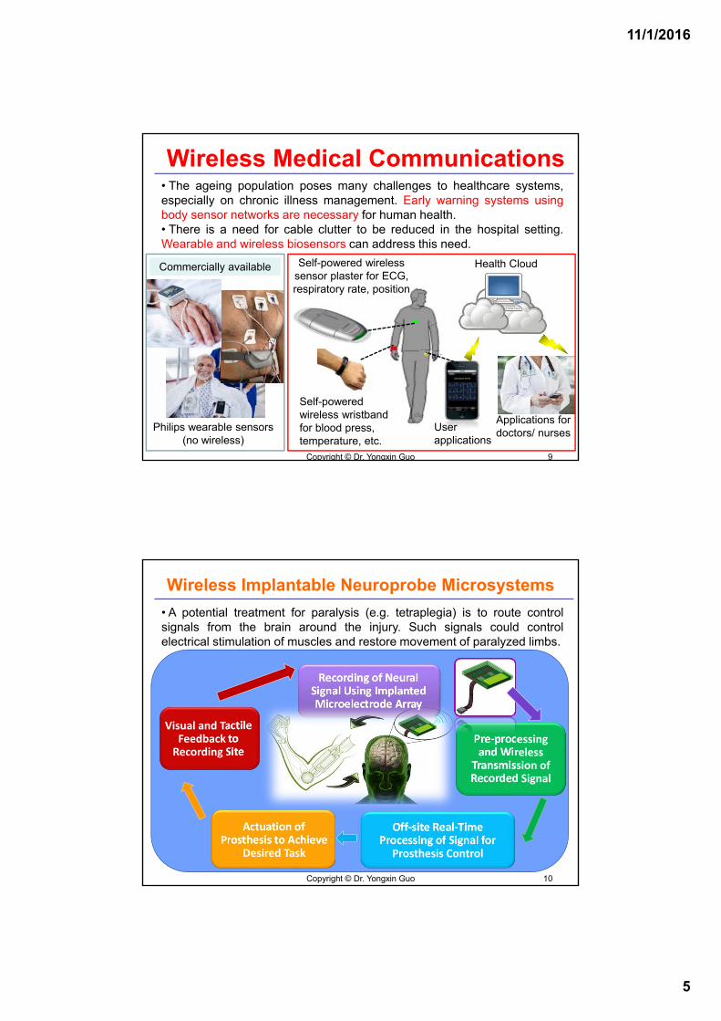
Wireless Medical Communications
Self-powered wireless wristband for blood press, temperature, etc.
User applications
• The ageing population poses many challenges to healthcare systems,especially on chronic illness management. Early warning systems usingbody sensor networks are necessary for human health.• There is a need for cable clutter to be reduced in the hospital setting.Wearable and wireless biosensors can address this need.
Health Cloud
Applications for doctors/ nurses
Self-powered wireless sensor plaster for ECG, respiratory rate, position
Commercially available
Philips wearable sensors(no wireless)
Copyright © Dr. Yongxin Guo 9
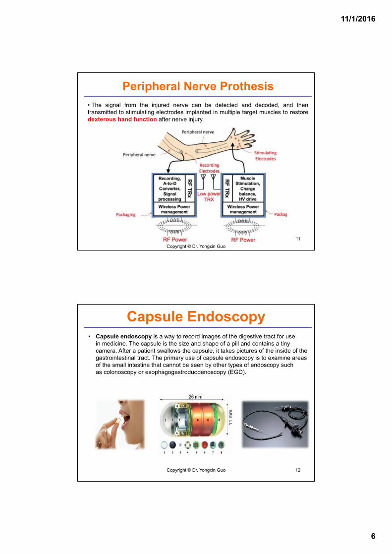
Wireless Implantable Neuroprobe Microsystems
Pre‐processing and Wireless
Transmission of Recorded Signal
Off‐site Real‐Time Processing of Signal for
Prosthesis Control
Actuation of Prosthesis to Achieve
Desired Task
Visual and Tactile Feedback to Recording Site
Recording of Neural Signal Using Implanted Microelectrode Array
• A potential treatment for paralysis (e.g. tetraplegia) is to route controlsignals from the brain around the injury. Such signals could controlelectrical stimulation of muscles and restore movement of paralyzed limbs.
Copyright © Dr. Yongxin Guo 10
11/1/2016
6
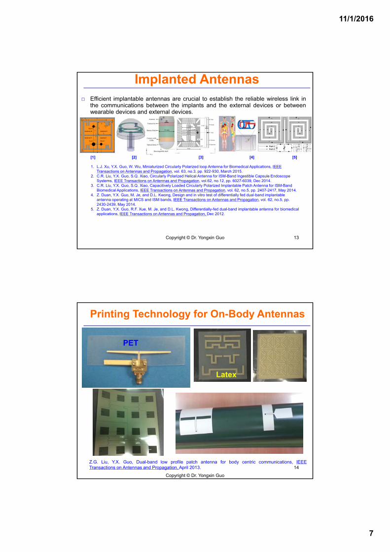
Peripheral Nerve Prothesis
HSIC2012, Nanjing
• The signal from the injured nerve can be detected and decoded, and thentransmitted to stimulating electrodes implanted in multiple target muscles to restoredexterous hand function after nerve injury.
Copyright © Dr. Yongxin Guo
11
Capsule Endoscopy
12Copyright © Dr. Yongxin Guo
• Capsule endoscopy is a way to record images of the digestive tract for use in medicine. The capsule is the size and shape of a pill and contains a tiny camera. After a patient swallows the capsule, it takes pictures of the inside of the gastrointestinal tract. The primary use of capsule endoscopy is to examine areas of the small intestine that cannot be seen by other types of endoscopy such as colonoscopy or esophagogastroduodenoscopy (EGD).
11/1/2016
7
Implanted Antennas Efficient implantable antennas are crucial to establish the reliable wireless link in
the communications between the implants and the external devices or betweenwearable devices and external devices.
1. L.J. Xu, Y.X. Guo, W. Wu, Miniaturized Circularly Polarized loop Antenna for Biomedical Applications, IEEE Transactions on Antennas and Propagation, vol. 63, no.3, pp. 922-930, March 2015.
2. C.R. Liu, Y.X. Guo, S.Q. Xiao, Circularly Polarized Helical Antenna for ISM-Band Ingestible Capsule Endoscope Systems, IEEE Transactions on Antennas and Propagation, vol.62, no.12, pp. 6027-6039, Dec 2014.
3. C.R. Liu, Y.X. Guo, S.Q. Xiao, Capacitively Loaded Circularly Polarized Implantable Patch Antenna for ISM-Band Biomedical Applications, IEEE Transactions on Antennas and Propagation, vol. 62, no.5, pp. 2407-2417, May 2014.
4. Z. Duan, Y.X. Guo, M. Je, and D.L. Kwong, Design and in vitro test of differentially fed dual-band implantable antenna operating at MICS and ISM bands, IEEE Transactions on Antennas and Propagation, vol. 62, no.5, pp. 2430-2439, May 2014.
5. Z. Duan, Y.X. Guo, R.F. Xue, M. Je, and D.L. Kwong, Differentially-fed dual-band implantable antenna for biomedicalapplications, IEEE Transactions on Antennas and Propagation, Dec 2012.
[1] [2] [3] [4] [5]
13Copyright © Dr. Yongxin Guo
Printing Technology for On-Body Antennas
HSIC2012, Nanjing
PET
Latex
Z.G. Liu, Y.X. Guo, Dual-band low profile patch antenna for body centric communications, IEEETransactions on Antennas and Propagation, April 2013.
Copyright © Dr. Yongxin Guo
14
11/1/2016
8
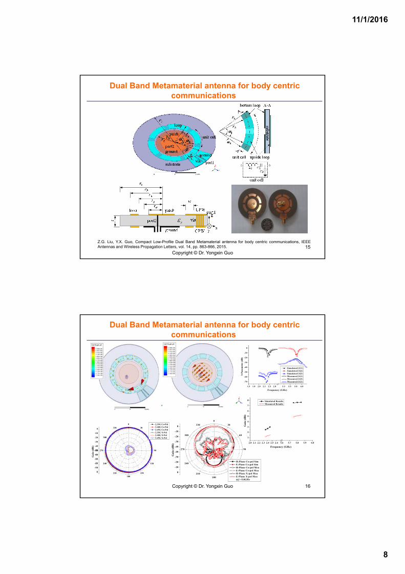
Dual Band Metamaterial antenna for body centric communications
HSIC2012, Nanjing
r
Z.G. Liu, Y.X. Guo, Compact Low-Profile Dual Band Metamaterial antenna for body centric communications, IEEEAntennas and Wireless Propagation Letters, vol. 14, pp. 863-866, 2015.
Copyright © Dr. Yongxin Guo15
Dual Band Metamaterial antenna for body centric communications
HSIC2012, Nanjing
-50
-40
-30
-20
-10
0
0
30
60
90
120
150
180
210
240
270
300
330
-50
-40
-30
-20
-10
0
Gai
n (
dB
i)
2.35G Co-Pol 2.40G Co-Pol 2.45G Co-Pol 2.35G X-Pol 2.40G X-Pol 2.45G X-Pol
-40
-30
-20
-10
0
0
30
60
90
120
150
180
210
240
270
300
330
-40
-30
-20
-10
0
Gai
n (
dB
i)
H-Plane Co-pol Sim E-Plane Co-pol Sim H-Plane Co-pol Mea E-Plane Co-pol Mea H-Plane X-pol Mea E-Plane X-pol Mea
@f =5.8GHz
1.5 1.8 2.0 2.3 2.5 2.8 5.3 5.5 5.8 6.0
-70
-60
-50
-40
-30
-20
-10
0
S P
aram
eter
(d
B)
Frequency (GHz)
Simulated |S11| Simulated |S22| Simulated |S21| Measured |S11| Measured |S22| Measured |S21|
2.0 2.1 2.2 2.3 2.4 2.5 2.6 5.6 5.7 5.8 5.9 6.0
1
2
3
4
5
6
7
8
Gai
n (
dB
i)
Frequency (GHz)
Simulated Results Measured Results
Copyright © Dr. Yongxin Guo 16
11/1/2016
9
MMIC Modelling & Packaging Lab
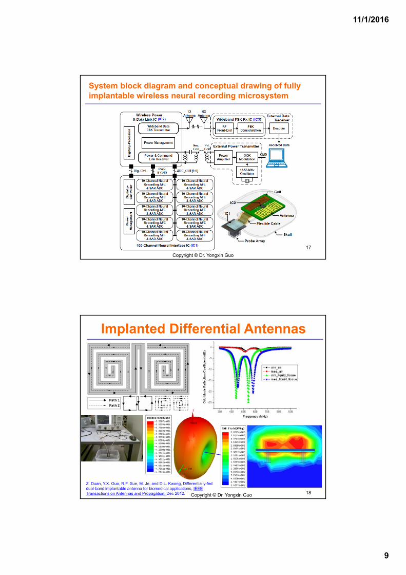
System block diagram and conceptual drawing of fully implantable wireless neural recording microsystem
Copyright © Dr. Yongxin Guo
17
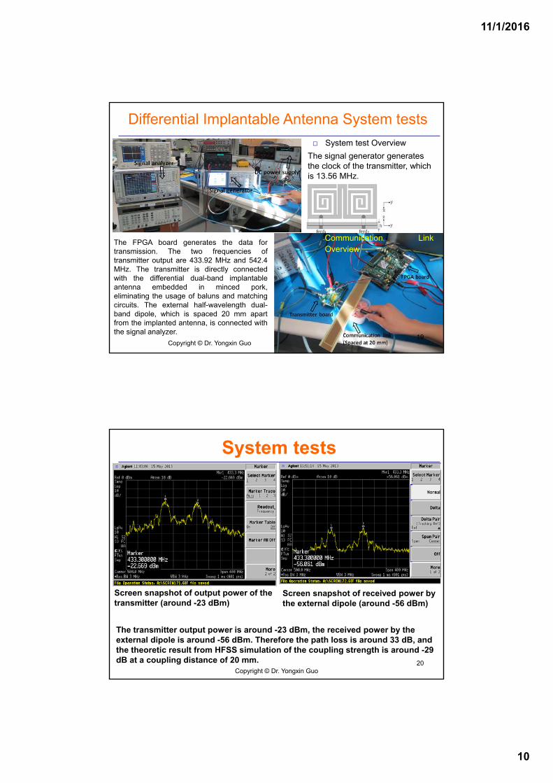
Implanted Differential Antennas
Z. Duan, Y.X. Guo, R.F. Xue, M. Je, and D.L. Kwong, Differentially-fed dual-band implantable antenna for biomedical applications, IEEE Transactions on Antennas and Propagation, Dec 2012. Copyright © Dr. Yongxin Guo 18
11/1/2016
10
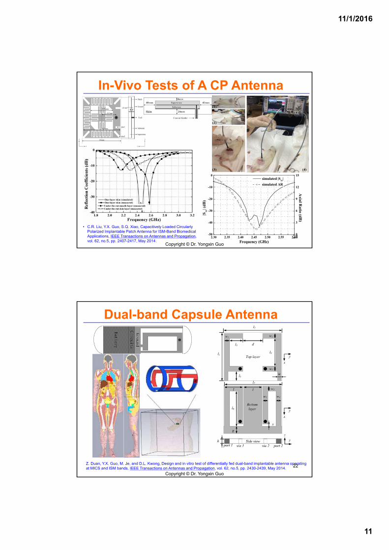
Differential Implantable Antenna System tests
System test Overview
Communication LinkOverview
The signal generator generates the clock of the transmitter, which is 13.56 MHz.
The FPGA board generates the data fortransmission. The two frequencies oftransmitter output are 433.92 MHz and 542.4MHz. The transmitter is directly connectedwith the differential dual-band implantableantenna embedded in minced pork,eliminating the usage of baluns and matchingcircuits. The external half-wavelength dual-band dipole, which is spaced 20 mm apartfrom the implanted antenna, is connected withthe signal analyzer.
Copyright © Dr. Yongxin Guo19
System tests
Screen snapshot of output power of the transmitter (around -23 dBm)
Screen snapshot of received power by the external dipole (around -56 dBm)
The transmitter output power is around -23 dBm, the received power by the external dipole is around -56 dBm. Therefore the path loss is around 33 dB, and the theoretic result from HFSS simulation of the coupling strength is around -29 dB at a coupling distance of 20 mm.
Copyright © Dr. Yongxin Guo20
11/1/2016
11
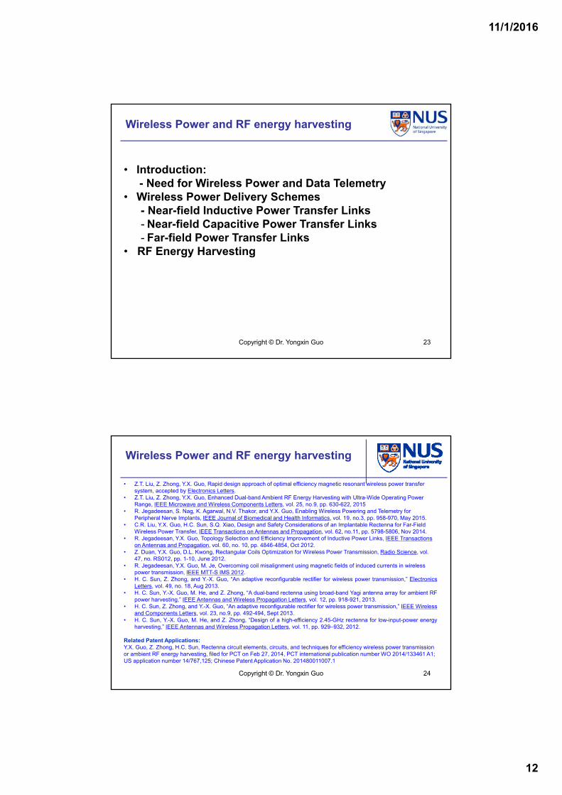
In-Vivo Tests of A CP Antenna
2.30 2.35 2.40 2.45 2.50 2.55 2.60-50
-40
-30
-20
-10
0 simulated |S
11|
simulated AR
Frequency (GHz)
|S11
| (d
B)
0
3
6
9
12
15
Axial R
atio (dB
)
• C.R. Liu, Y.X. Guo, S.Q. Xiao, Capacitively Loaded Circularly Polarized Implantable Patch Antenna for ISM-Band Biomedical Applications, IEEE Transactions on Antennas and Propagation, vol. 62, no.5, pp. 2407-2417, May 2014.
Copyright © Dr. Yongxin Guo
21
Dual-band Capsule Antenna
Z. Duan, Y.X. Guo, M. Je, and D.L. Kwong, Design and in vitro test of differentially fed dual-band implantable antenna operating at MICS and ISM bands, IEEE Transactions on Antennas and Propagation, vol. 62, no.5, pp. 2430-2439, May 2014.
Copyright © Dr. Yongxin Guo
22
11/1/2016
12
• Introduction:- Need for Wireless Power and Data Telemetry
• Wireless Power Delivery Schemes - Near-field Inductive Power Transfer Links- Near-field Capacitive Power Transfer Links- Far-field Power Transfer Links
• RF Energy Harvesting
23Copyright © Dr. Yongxin Guo
Wireless Power and RF energy harvesting
Wireless Power and RF energy harvesting
• Z.T. Liu, Z. Zhong, Y.X. Guo, Rapid design approach of optimal efficiency magnetic resonant wireless power transfer system, accepted by Electronics Letters.
• Z.T. Liu, Z. Zhong, Y.X. Guo, Enhanced Dual-band Ambient RF Energy Harvesting with Ultra-Wide Operating Power Range, IEEE Microwave and Wireless Components Letters, vol. 25, no.9, pp. 630-622, 2015
• R. Jegadeesan, S. Nag, K. Agarwal, N.V. Thakor, and Y.X. Guo, Enabling Wireless Powering and Telemetry for Peripheral Nerve Implants, IEEE Journal of Biomedical and Health Informatics, vol. 19, no.3, pp. 958-970, May 2015.
• C.R. Liu, Y.X. Guo, H.C. Sun, S.Q. Xiao, Design and Safety Considerations of an Implantable Rectenna for Far-Field Wireless Power Transfer, IEEE Transactions on Antennas and Propagation, vol. 62, no.11, pp. 5798-5806, Nov 2014.
• R. Jegadeesan, Y.X. Guo, Topology Selection and Efficiency Improvement of Inductive Power Links, IEEE Transactions on Antennas and Propagation, vol. 60, no. 10, pp. 4846-4854, Oct 2012.
• Z. Duan, Y.X. Guo, D.L. Kwong, Rectangular Coils Optimization for Wireless Power Transmission, Radio Science, vol. 47, no. RS012, pp. 1-10, June 2012.
• R. Jegadeesan, Y.X. Guo, M. Je, Overcoming coil misalignment using magnetic fields of induced currents in wireless power transmission, IEEE MTT-S IMS 2012.
• H. C. Sun, Z. Zhong, and Y.-X. Guo, “An adaptive reconfigurable rectifier for wireless power transmission,” ElectronicsLetters, vol. 49, no. 18, Aug 2013.
• H. C. Sun, Y.-X. Guo, M. He, and Z. Zhong, “A dual-band rectenna using broad-band Yagi antenna array for ambient RFpower harvesting,” IEEE Antennas and Wireless Propagation Letters, vol. 12, pp. 918-921, 2013.
• H. C. Sun, Z. Zhong, and Y.-X. Guo, “An adaptive reconfigurable rectifier for wireless power transmission,” IEEE Wirelessand Components Letters, vol. 23, no.9, pp. 492-494, Sept 2013.
• H. C. Sun, Y.-X. Guo, M. He, and Z. Zhong, “Design of a high-efficiency 2.45-GHz rectenna for low-input-power energyharvesting,” IEEE Antennas and Wireless Propagation Letters, vol. 11, pp. 929–932, 2012.
Related Patent Applications:Y.X. Guo, Z. Zhong, H.C. Sun, Rectenna circuit elements, circuits, and techniques for efficiency wireless power transmission or ambient RF energy harvesting, filed for PCT on Feb 27, 2014, PCT international publication number WO 2014/133461 A1; US application number 14/767,125; Chinese Patent Application No. 201480011007.1
Copyright © Dr. Yongxin Guo 24
11/1/2016
13
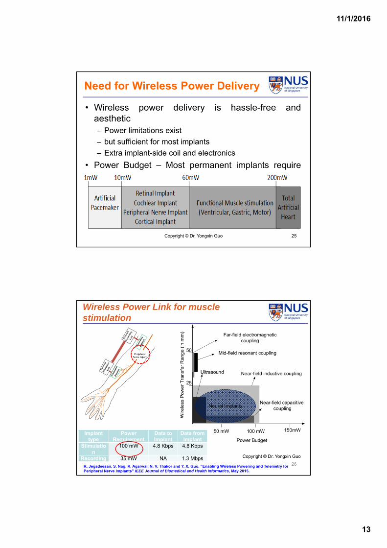
Need for Wireless Power Delivery
• Wireless power delivery is hassle-free andaesthetic– Power limitations exist
– but sufficient for most implants
– Extra implant-side coil and electronics
• Power Budget – Most permanent implants requirepower less than 60mW.
25Copyright © Dr. Yongxin Guo
0.20λo× 0.20λo 0.18λo× 0.18λo
Power Budget
Wire
less
Pow
er
Tra
nsf
er
Ran
ge
(in m
m)
150mW50 mW 100 mW
Ultrasound
Far-field electromagnetic coupling
Mid-field resonant coupling
Near-field inductive coupling
25
50
Near-field capacitive couplingNeural Implants
Wireless Power Link for muscle stimulation
Peripheral Nerve Injury
Implant type
Power Requirement
Data toImplant
Data from Implant
Stimulation
100 mW 4.8 Kbps 4.8 Kbps
Recording 35 mW NA 1.3 Mbps
R. Jegadeesan, S. Nag, K. Agarwal, N. V. Thakor and Y. X. Guo, “Enabling Wireless Powering and Telemetry for Peripheral Nerve Implants” IEEE Journal of Biomedical and Health Informatics, May 2015.
26
Copyright © Dr. Yongxin Guo
11/1/2016
14
MMIC Modelling & Packaging Lab
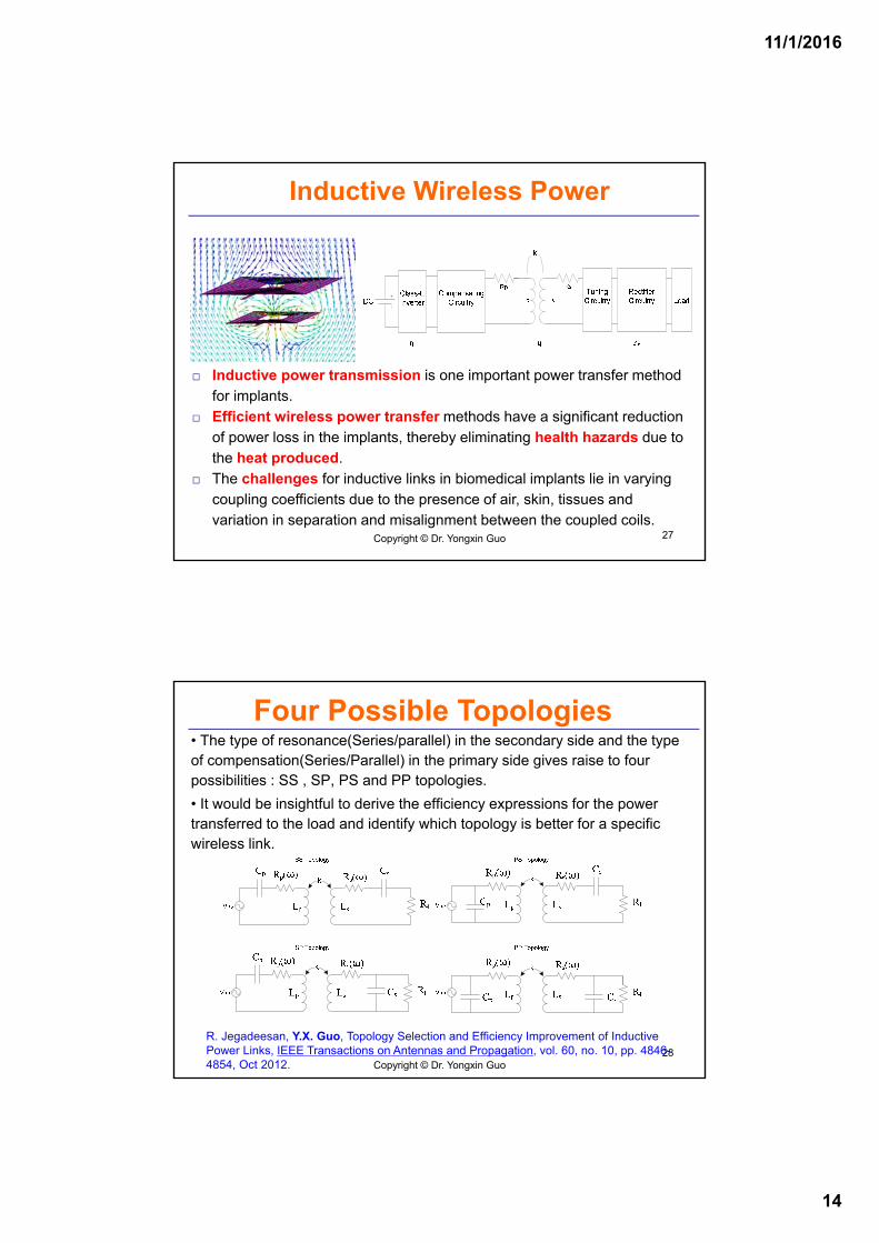
Inductive Wireless Power
Inductive power transmission is one important power transfer method
for implants.
Efficient wireless power transfer methods have a significant reduction
of power loss in the implants, thereby eliminating health hazards due to
the heat produced.
The challenges for inductive links in biomedical implants lie in varying
coupling coefficients due to the presence of air, skin, tissues and
variation in separation and misalignment between the coupled coils.Copyright © Dr. Yongxin Guo 27
Four Possible Topologies• The type of resonance(Series/parallel) in the secondary side and the type of compensation(Series/Parallel) in the primary side gives raise to four possibilities : SS , SP, PS and PP topologies.
• It would be insightful to derive the efficiency expressions for the power transferred to the load and identify which topology is better for a specific wireless link.
HSIC2012, Nanjing
R. Jegadeesan, Y.X. Guo, Topology Selection and Efficiency Improvement of Inductive Power Links, IEEE Transactions on Antennas and Propagation, vol. 60, no. 10, pp. 4846-4854, Oct 2012. Copyright © Dr. Yongxin Guo
28
11/1/2016
15
29
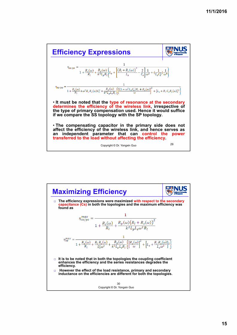
Efficiency Expressions
• It must be noted that the type of resonance at the secondarydetermines the efficiency of the wireless link, irrespective ofthe type of primary compensation used. Hence it would sufficeif we compare the SS topology with the SP topology.
• The compensating capacitor in the primary side does notaffect the efficiency of the wireless link, and hence serves asan independent parameter that can control the powertransferred to the load without affecting the efficiency.
Copyright © Dr. Yongxin Guo
30
Maximizing Efficiency The efficiency expressions were maximized with respect to the secondary
capacitance (Cs) in both the topologies and the maximum efficiency was found as
It is to be noted that in both the topologies the coupling coefficient enhances the efficiency and the series resistances degrades the efficiency.
However the effect of the load resistance, primary and secondary inductance on the efficiencies are different for both the topologies.
Copyright © Dr. Yongxin Guo
11/1/2016
16
31
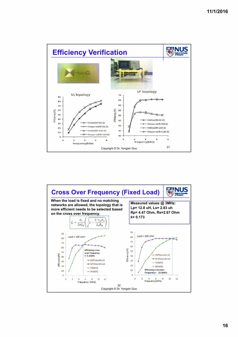
Efficiency Verification
Copyright © Dr. Yongxin Guo
32
Cross Over Frequency (Fixed Load)When the load is fixed and no matching networks are allowed, the topology that is more efficient needs to be selected based on the cross over frequency.
Measured values @ 3MHz:Lp= 12.8 uH, Ls= 2.83 uhRp= 4.47 Ohm, Rs=2.67 Ohmk= 0.173
Copyright © Dr. Yongxin Guo
11/1/2016
17
33
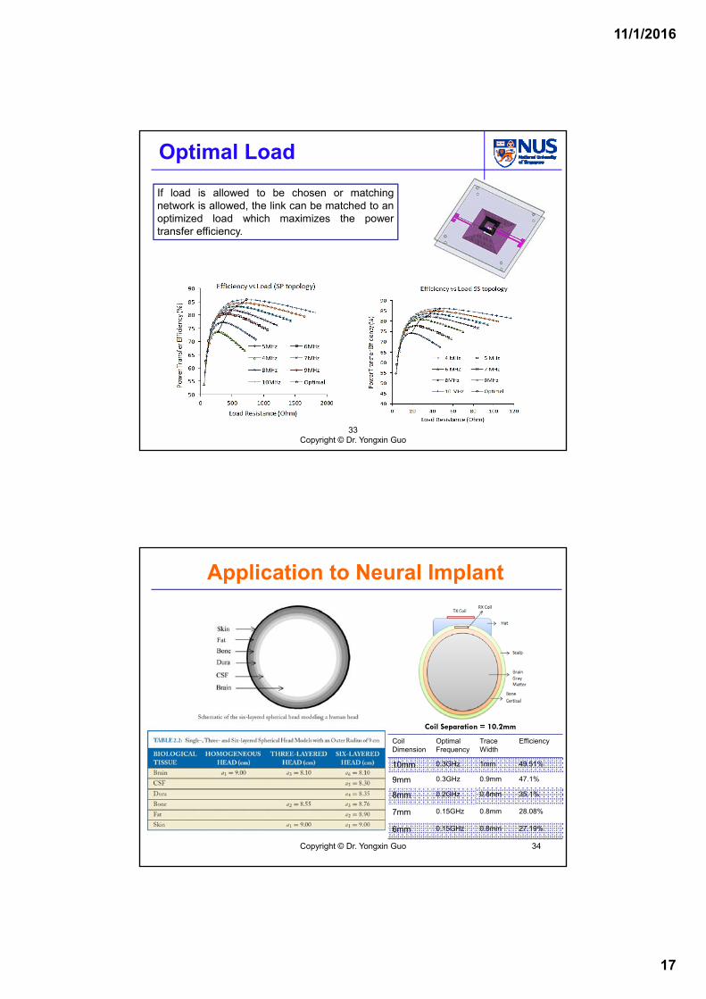
Optimal Load
If load is allowed to be chosen or matchingnetwork is allowed, the link can be matched to anoptimized load which maximizes the powertransfer efficiency.
Copyright © Dr. Yongxin Guo
Application to Neural Implant
Coil Dimension
Optimal Frequency
TraceWidth
Efficiency
10mm 0.3GHz 1mm 49.51%
9mm 0.3GHz 0.9mm 47.1%
8mm 0.2GHz 0.8mm 35.1%
7mm 0.15GHz 0.8mm 28.08%
6mm 0.15GHz 0.8mm 27.19%
Coil Separation = 10.2mm
Copyright © Dr. Yongxin Guo 34
11/1/2016
18
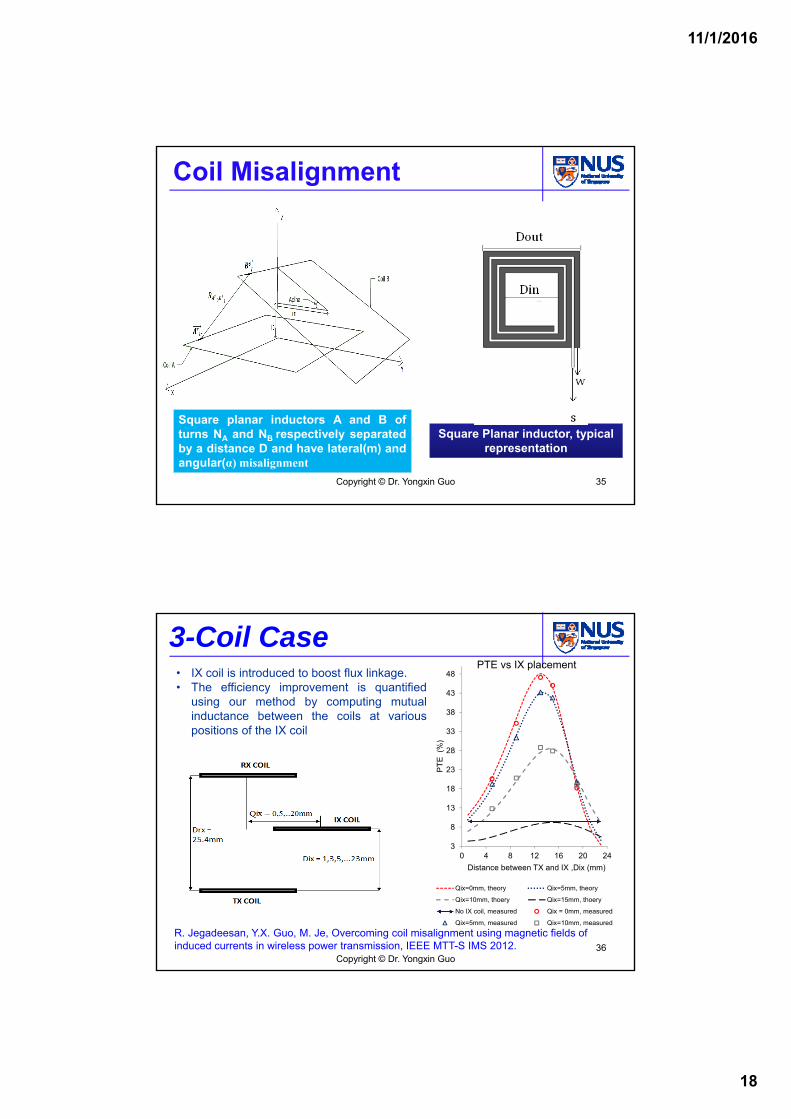
Coil Misalignment
Square Planar inductor, typical representation
Square planar inductors A and B ofturns NA and NB respectively separatedby a distance D and have lateral(m) andangular(α) misalignment
Copyright © Dr. Yongxin Guo 35
3-Coil Case
3
8
13
18
23
28
33
38
43
48
0 4 8 12 16 20 24
PT
E (
%)
Distance between TX and IX ,Dix (mm)
PTE vs IX placement
Qix=0mm, theory Qix=5mm, theory
Qix=10mm, thoery Qix=15mm, thoery
No IX coil, measured Qix = 0mm, measured
Qix=5mm, measured Qix=10mm, measured
• IX coil is introduced to boost flux linkage.• The efficiency improvement is quantified
using our method by computing mutualinductance between the coils at variouspositions of the IX coil
R. Jegadeesan, Y.X. Guo, M. Je, Overcoming coil misalignment using magnetic fields of induced currents in wireless power transmission, IEEE MTT-S IMS 2012.
Copyright © Dr. Yongxin Guo36
11/1/2016
19
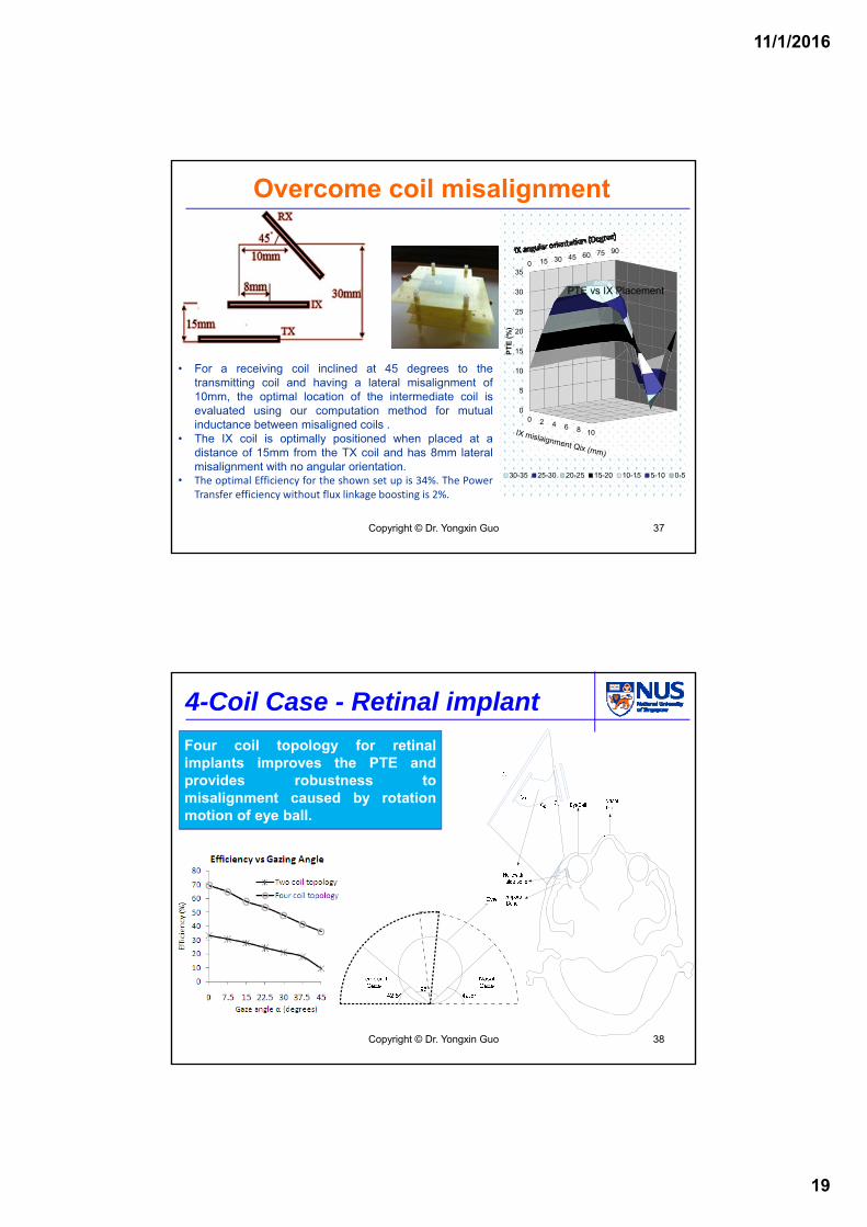
Overcome coil misalignment
0 15 30 45 60 75 90
0
5
10
15
20
25
30
35
0 2 4 6 8 10
PT
E (
%)
PTE vs IX Placement
30-35 25-30 20-25 15-20 10-15 5-10 0-5
• For a receiving coil inclined at 45 degrees to thetransmitting coil and having a lateral misalignment of10mm, the optimal location of the intermediate coil isevaluated using our computation method for mutualinductance between misaligned coils .
• The IX coil is optimally positioned when placed at adistance of 15mm from the TX coil and has 8mm lateralmisalignment with no angular orientation.
• The optimal Efficiency for the shown set up is 34%. The PowerTransfer efficiency without flux linkage boosting is 2%.
Copyright © Dr. Yongxin Guo 37
4-Coil Case - Retinal implant
Four coil topology for retinalimplants improves the PTE andprovides robustness tomisalignment caused by rotationmotion of eye ball.
Copyright © Dr. Yongxin Guo 38
11/1/2016
20
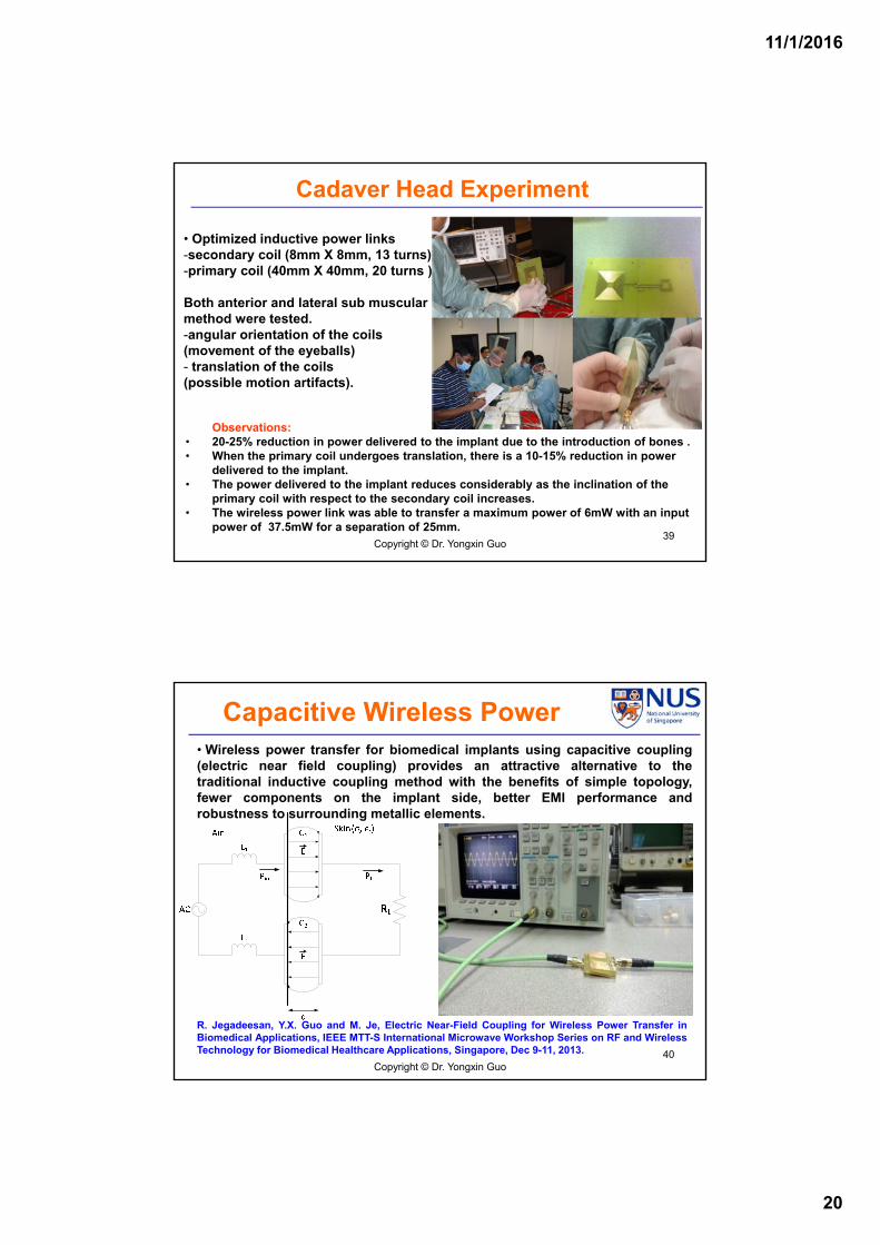
Cadaver Head Experiment
• Optimized inductive power links-secondary coil (8mm X 8mm, 13 turns) -primary coil (40mm X 40mm, 20 turns )
Both anterior and lateral sub muscular method were tested. -angular orientation of the coils (movement of the eyeballs) - translation of the coils (possible motion artifacts).
Observations:• 20-25% reduction in power delivered to the implant due to the introduction of bones .• When the primary coil undergoes translation, there is a 10-15% reduction in power
delivered to the implant.• The power delivered to the implant reduces considerably as the inclination of the
primary coil with respect to the secondary coil increases.• The wireless power link was able to transfer a maximum power of 6mW with an input
power of 37.5mW for a separation of 25mm.Copyright © Dr. Yongxin Guo
39
Capacitive Wireless Power
HSIC2012, Nanjing
• Wireless power transfer for biomedical implants using capacitive coupling(electric near field coupling) provides an attractive alternative to thetraditional inductive coupling method with the benefits of simple topology,fewer components on the implant side, better EMI performance androbustness to surrounding metallic elements.
R. Jegadeesan, Y.X. Guo and M. Je, Electric Near-Field Coupling for Wireless Power Transfer inBiomedical Applications, IEEE MTT-S International Microwave Workshop Series on RF and WirelessTechnology for Biomedical Healthcare Applications, Singapore, Dec 9-11, 2013. 40
Copyright © Dr. Yongxin Guo
11/1/2016
21
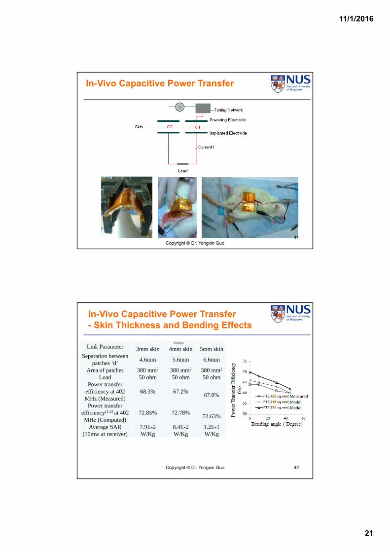
In-Vivo Capacitive Power Transfer
41Copyright © Dr. Yongxin Guo
Link ParameterValues
3mm skin 4mm skin 5mm skinSeparation between
patches ‘d’4.6mm 5.6mm 6.6mm
Area of patches 380 mm2 380 mm2 380 mm2
Load 50 ohm 50 ohm 50 ohmPower transfer
efficiency at 402 MHz (Measured)
68.3% 67.2%67.0%
Power transfer efficiency[1-2] at 402 MHz (Computed)
72.85% 72.78%72.63%
Average SAR (10mw at receiver)
7.9E-2 W/Kg
8.4E-2W/Kg
1.2E-1 W/Kg
42
In-Vivo Capacitive Power Transfer- Skin Thickness and Bending Effects
Copyright © Dr. Yongxin Guo
11/1/2016
22
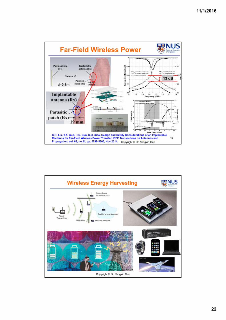
Far-Field Wireless Power
HSIC2012, Nanjing
C.R. Liu, Y.X. Guo, H.C. Sun, S.Q. Xiao, Design and Safety Considerations of an Implantable Rectenna for Far-Field Wireless Power Transfer, IEEE Transactions on Antennas and Propagation, vol. 62, no.11, pp. 5798-5806, Nov 2014.
43
13 dB
d=0.5m
Copyright © Dr. Yongxin Guo
Wireless Energy Harvesting
Copyright © Dr. Yongxin Guo44

11/1/2016
23
RectifierPower Storage
ImpedanceTransformation
Band passfilter
(BPF)
Antenna
A rectenna is a rectifying antenna, a special type of antenna that is used to directly convertmicrowave energy into DC electricity.
A simplest rectenna element consists of an antenna (or antenna array) with a Schottky diodeplaced across the antenna elements. The diode rectifies the RF current induced in the antennaby the microwaves, to produce DC power. Schottky diodes are used because they have thelowest voltage drop and highest speed and therefore waste the least amount of power due toconduction and switching. Good rectennas consist of impedance transformation, band passfilter and low pass filter to improve its RF-DC conversion efficiency .
Low passfilter
(LPF)
Rectenna Design for Wireless Power Transmission
Copyright © Dr. Yongxin Guo45
Adaptive Rectifier Design
Research on Wireless Power Transmission
Fig. 1. Overview of the wireless power transmission system.
Pin changes if
• Pt varies
• d changes
Requirementfor rectifier High efficiency
over wide inputpower range.
Requirement for Rectifier Design
• Receiving antennais on mobile devices.
Copyright © Dr. Yongxin Guo 46

11/1/2016
24
Diode Selection for Rectifier
•Threshold Voltage (Vth)
•Breakdown Voltage (Vbr)
determinesrectifier’s efficiency at low input power.
rectifier’s efficiency at high input power. determines
Low Vth is preferred for low-input-power applications.
High Vbr is preferred for high-input-power applications.
Limitation of Normal Rectifier
Low Vth and high Vbr cannot be obtained at the same time.
High efficiency can only be achieved in a narrow input power range.
Adaptive Rectifier Design
Copyright © Dr. Yongxin Guo 47
Research on Wireless Power Transmission
Limitation Illustration
(a) Single shunt-mounted diode.
(b) Two shunt-mounted diodes.
low Vth
low Vbr
high Vthhigh Vbr
-25 -20 -15 -10 -5 0 5 10 15 20 250
10
20
30
40
50
60
70
80
90
Eff
icie
nc
y (
%)
Input Power (dBm)
Eff (a) Eff (b)
• Rectifier (a) is only suitable for low-input-power applications.
• Rectifier (b) is only suitable for high-input-power applications.
Efficiencies versus input power.
Adaptive Rectifier Design
Copyright © Dr. Yongxin Guo 48
11/1/2016
25
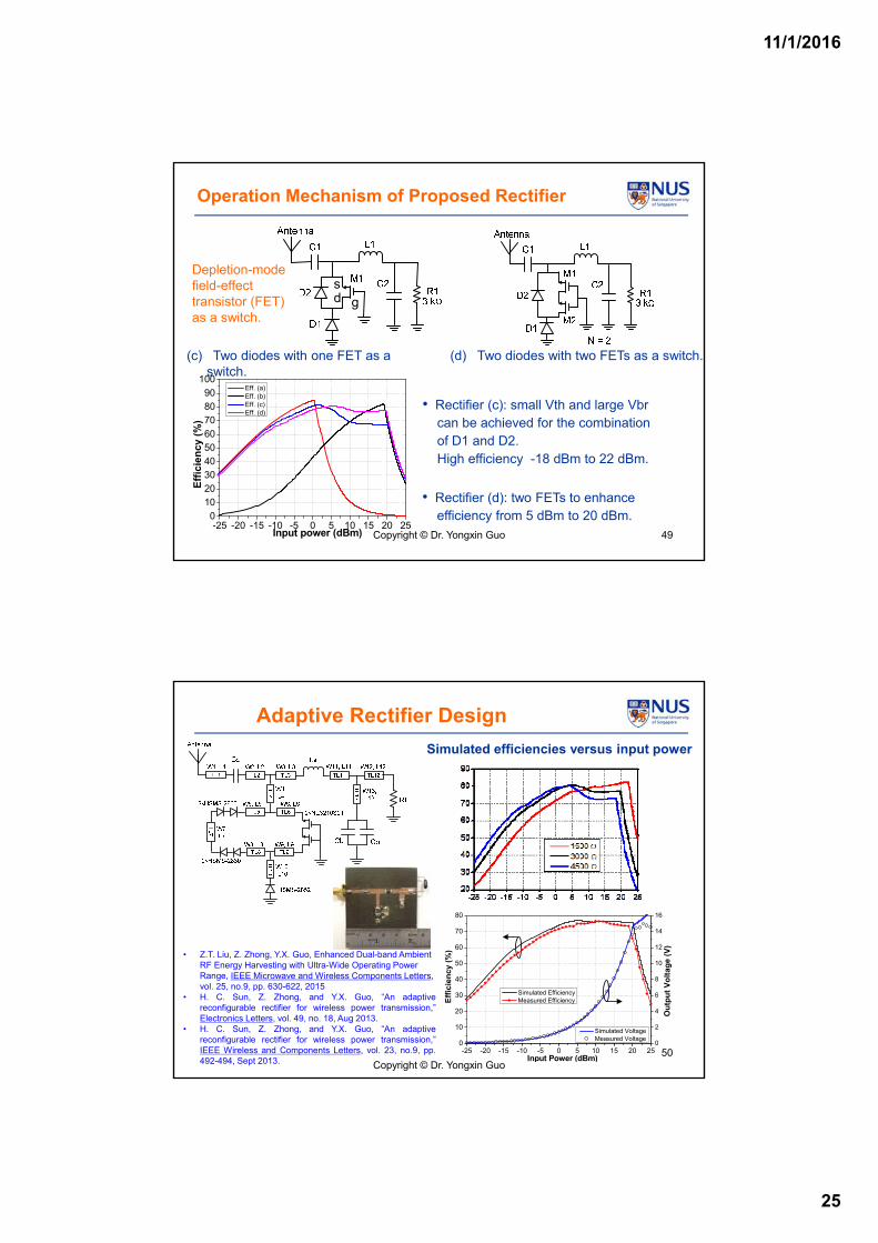
Operation Mechanism of Proposed Rectifier
(d) Two diodes with two FETs as a switch.
• Rectifier (c): small Vth and large Vbrcan be achieved for the combinationof D1 and D2.High efficiency -18 dBm to 22 dBm.
(c) Two diodes with one FET as a switch.
• Rectifier (d): two FETs to enhance efficiency from 5 dBm to 20 dBm.
-25 -20 -15 -10 -5 0 5 10 15 20 250
1020
30405060
708090
100
Eff
icie
ncy
(%
)
Input power (dBm)
Eff. (a) Eff. (b) Eff. (c) Eff. (d)
sgd
Depletion-mode field-effect transistor (FET) as a switch.
Copyright © Dr. Yongxin Guo 49
0
10
20
30
40
50
60
70
80
-25 -20 -15 -10 -5 0 5 10 15 20 250
2
4
6
8
10
12
14
16
Ou
tpu
t V
olt
age (
V)
Eff
icie
ncy
(%
)
Input Power (dBm)
Simulated Efficiency Measured Efficiency
Simulated Voltage Measured Voltage
Simulated efficiencies versus input power
Adaptive Rectifier Design
Copyright © Dr. Yongxin Guo50
• Z.T. Liu, Z. Zhong, Y.X. Guo, Enhanced Dual-band Ambient RF Energy Harvesting with Ultra-Wide Operating Power Range, IEEE Microwave and Wireless Components Letters, vol. 25, no.9, pp. 630-622, 2015
• H. C. Sun, Z. Zhong, and Y.X. Guo, “An adaptivereconfigurable rectifier for wireless power transmission,”Electronics Letters, vol. 49, no. 18, Aug 2013.
• H. C. Sun, Z. Zhong, and Y.X. Guo, “An adaptivereconfigurable rectifier for wireless power transmission,”IEEE Wireless and Components Letters, vol. 23, no.9, pp.492-494, Sept 2013.
11/1/2016
26
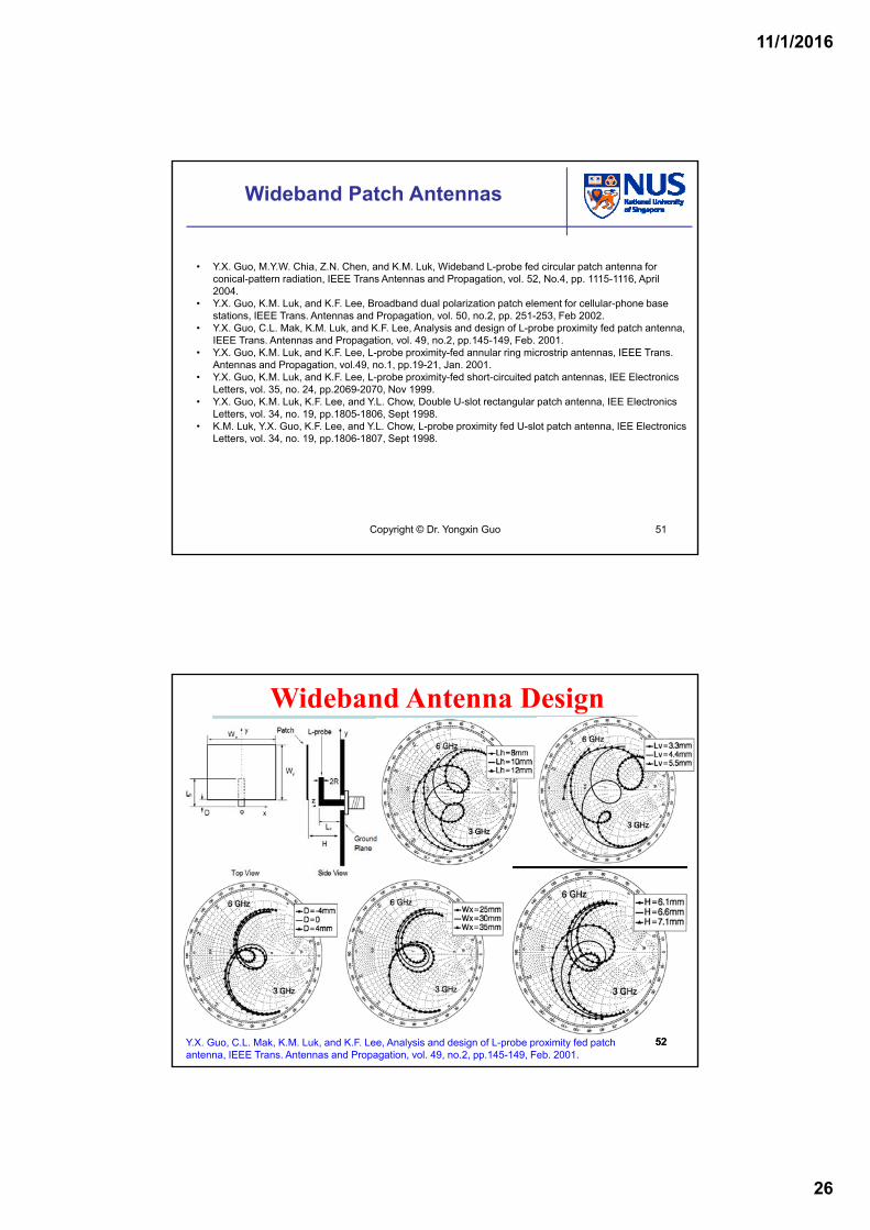
Wideband Patch Antennas
• Y.X. Guo, M.Y.W. Chia, Z.N. Chen, and K.M. Luk, Wideband L-probe fed circular patch antenna for conical-pattern radiation, IEEE Trans Antennas and Propagation, vol. 52, No.4, pp. 1115-1116, April 2004.
• Y.X. Guo, K.M. Luk, and K.F. Lee, Broadband dual polarization patch element for cellular-phone base stations, IEEE Trans. Antennas and Propagation, vol. 50, no.2, pp. 251-253, Feb 2002.
• Y.X. Guo, C.L. Mak, K.M. Luk, and K.F. Lee, Analysis and design of L-probe proximity fed patch antenna, IEEE Trans. Antennas and Propagation, vol. 49, no.2, pp.145-149, Feb. 2001.
• Y.X. Guo, K.M. Luk, and K.F. Lee, L-probe proximity-fed annular ring microstrip antennas, IEEE Trans. Antennas and Propagation, vol.49, no.1, pp.19-21, Jan. 2001.
• Y.X. Guo, K.M. Luk, and K.F. Lee, L-probe proximity-fed short-circuited patch antennas, IEE Electronics Letters, vol. 35, no. 24, pp.2069-2070, Nov 1999.
• Y.X. Guo, K.M. Luk, K.F. Lee, and Y.L. Chow, Double U-slot rectangular patch antenna, IEE Electronics Letters, vol. 34, no. 19, pp.1805-1806, Sept 1998.
• K.M. Luk, Y.X. Guo, K.F. Lee, and Y.L. Chow, L-probe proximity fed U-slot patch antenna, IEE Electronics Letters, vol. 34, no. 19, pp.1806-1807, Sept 1998.
Copyright © Dr. Yongxin Guo 51
Wideband Antenna Design
52Y.X. Guo, C.L. Mak, K.M. Luk, and K.F. Lee, Analysis and design of L-probe proximity fed patch antenna, IEEE Trans. Antennas and Propagation, vol. 49, no.2, pp.145-149, Feb. 2001.
52
11/1/2016
27
MMIC Modelling & Packaging Lab
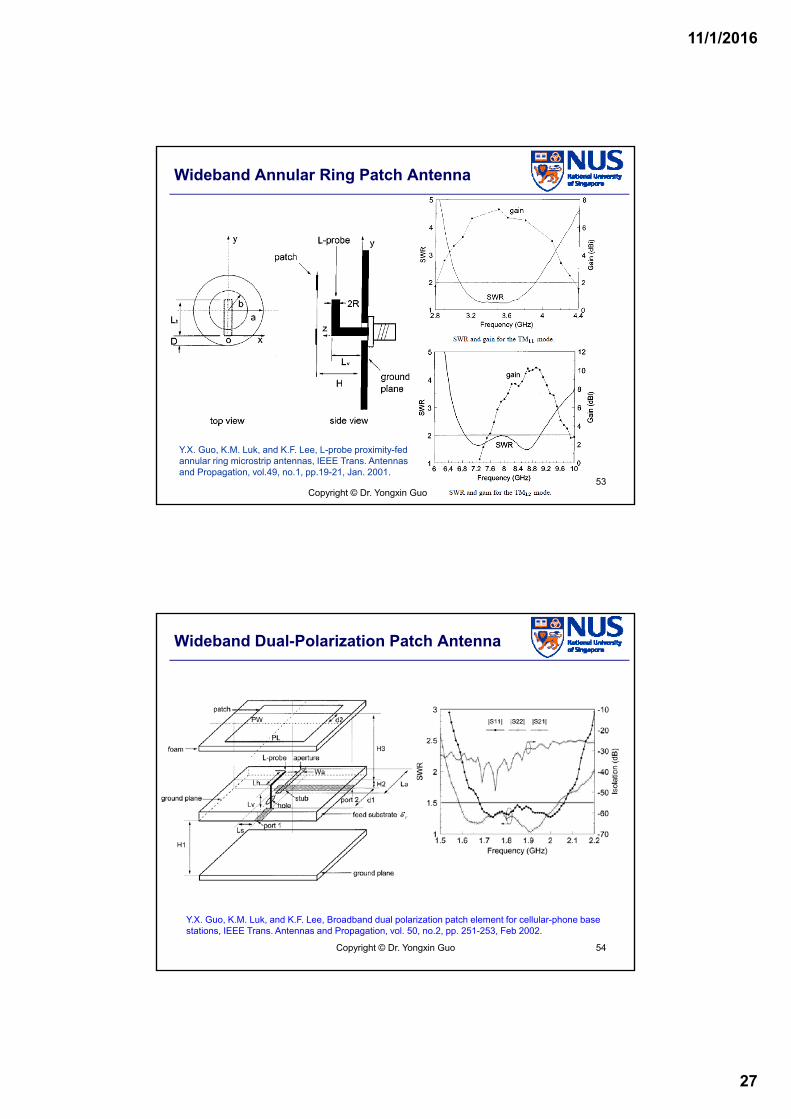
Wideband Annular Ring Patch Antenna
Y.X. Guo, K.M. Luk, and K.F. Lee, L-probe proximity-fed annular ring microstrip antennas, IEEE Trans. Antennas and Propagation, vol.49, no.1, pp.19-21, Jan. 2001.
Copyright © Dr. Yongxin Guo53
MMIC Modelling & Packaging Lab
Wideband Dual-Polarization Patch Antenna
Y.X. Guo, K.M. Luk, and K.F. Lee, Broadband dual polarization patch element for cellular-phone base stations, IEEE Trans. Antennas and Propagation, vol. 50, no.2, pp. 251-253, Feb 2002.
Copyright © Dr. Yongxin Guo 54

11/1/2016
28
MMIC Modelling & Packaging Lab
Wideband Patch Antenna with Conical Radiation Pattern
Y.X. Guo, M.Y.W. Chia, Z.N. Chen, and K.M. Luk, Wideband L-probe fed circular patch antenna for conical-pattern radiation, IEEE Trans Antennas and Propagation, vol. 52, No.4, pp. 1115-1116, April 2004.
Copyright © Dr. Yongxin Guo55
MMIC Modelling & Packaging Lab
Wideband Patch Antennas with Broadband Feeding Networks
• Z.Y. Zhang, Y.X. Guo, L.C. Ong, and M.Y.W. Chia, “A new wideband planar balun on a single-layerPCB”, IEEE Microwave and Wireless Components Letters, vol. 15, no.6, pp. 416-418, 2005.
• Y. X. Guo, Z. Y. Zhang, and L. C. Ong, “Improved wideband Schiffman phase shifter,” IEEE Trans.Microw. Theory Tech. , vol. 54, no. 3, pp. 1196-1200, Mar. 2006.
• L. Bian, Y. X. Guo, L. C. Ong, and X. Q. Shi, “Wideband Circularly Polarized Patch Antenna,”IEEE Trans.Antennas Propag. , vol. 54, no. 9, pp. 2682-2686, Sep. 2006.
• Y.X. Guo, K.W. Khoo, L.C. Ong, and K.M. Luk, Wideband Low Cross-Polarization Patch Antenna UsingA Broadband Balun Feed Network, Radio Science, vol. 42, RS5008, doi:10.1029/2006RS003595, Oct2007.
• Y.X. Guo, K.W. Khoo, L.C. Ong, Wideband dual-polarized planar antenna with broadband baluns, IEEETransaction on Antennas and Propagation, vol. 55, no.1, pp. 78-83, Jan 2007.
• Y.X. Guo, K.W. Khoo, L.C. Ong, Wideband Circularly-Polarized planar antenna with broadband baluns,IEEE Transaction on Antennas and Propagation, vol. 56, no.2, pp. 319-326, Feb 2008.
• Y.X. Guo, L. Bian, X.Q. Shi, Wideband Circularly Polarized Annular-Ring Microstrip Antenna, IEEETransactions on Antennas and Propagation, vol. 57, no. 8, pp. 2474-2477.
Copyright © Dr. Yongxin Guo 56
11/1/2016
29
MMIC Modelling & Packaging Lab
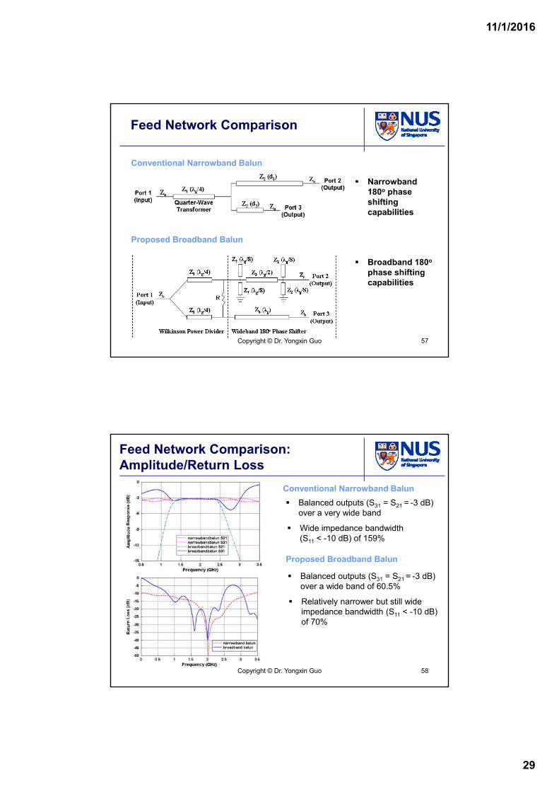
Feed Network Comparison
Conventional Narrowband Balun
Proposed Broadband Balun
Narrowband 180o phase shifting capabilities
Broadband 180o
phase shifting capabilities
Copyright © Dr. Yongxin Guo 57
MMIC Modelling & Packaging Lab
Feed Network Comparison: Amplitude/Return Loss
Conventional Narrowband Balun
Proposed Broadband Balun
Balanced outputs (S31 = S21 = -3 dB) over a very wide band
Balanced outputs (S31 = S21 = -3 dB) over a wide band of 60.5%
Wide impedance bandwidth (S11 < -10 dB) of 159%
Relatively narrower but still wide impedance bandwidth (S11 < -10 dB) of 70%
Copyright © Dr. Yongxin Guo 58
11/1/2016
30
MMIC Modelling & Packaging Lab
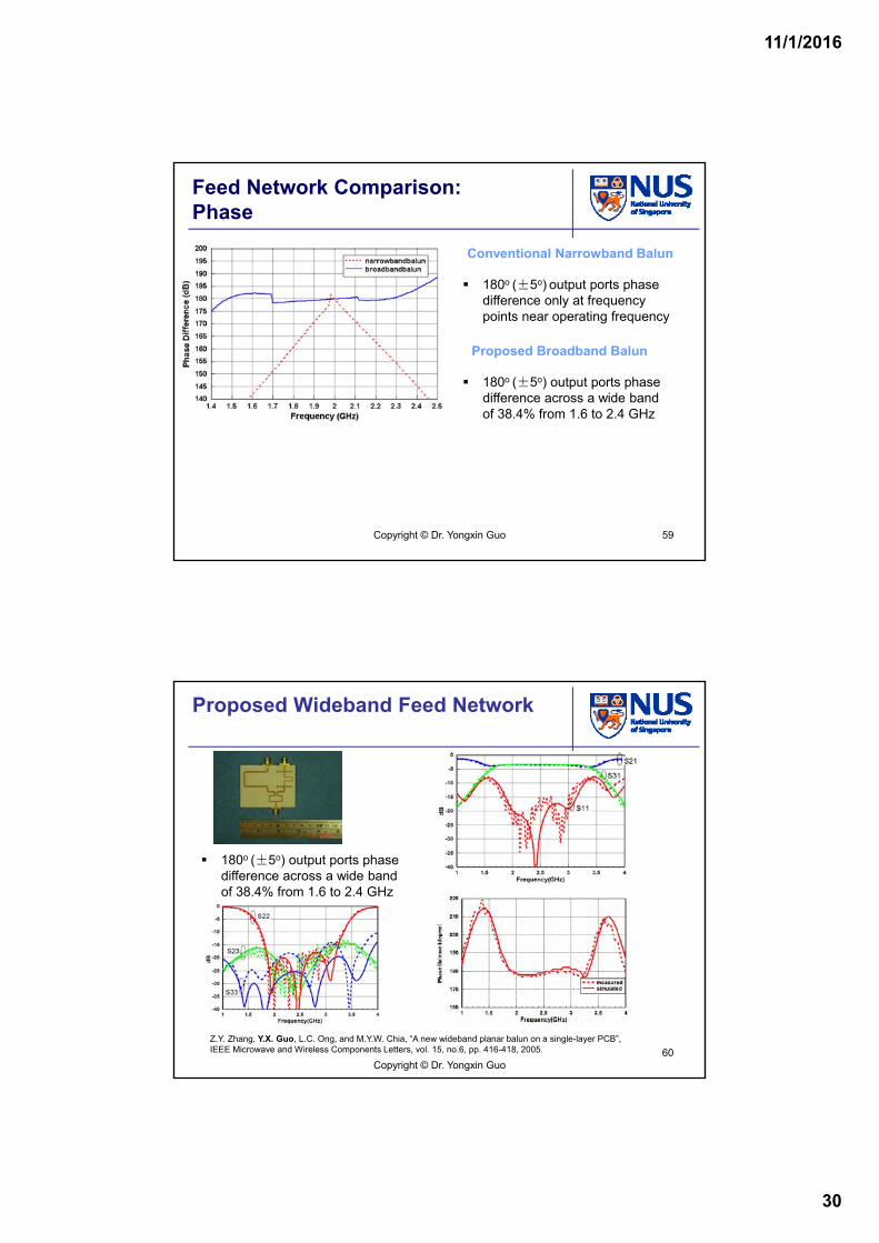
Feed Network Comparison: Phase
Conventional Narrowband Balun
Proposed Broadband Balun
180o (±5o) output ports phase difference only at frequency points near operating frequency
180o (±5o) output ports phase difference across a wide band of 38.4% from 1.6 to 2.4 GHz
Copyright © Dr. Yongxin Guo 59
MMIC Modelling & Packaging Lab
Proposed Wideband Feed Network
180o (±5o) output ports phase difference across a wide band of 38.4% from 1.6 to 2.4 GHz
Z.Y. Zhang, Y.X. Guo, L.C. Ong, and M.Y.W. Chia, “A new wideband planar balun on a single-layer PCB”, IEEE Microwave and Wireless Components Letters, vol. 15, no.6, pp. 416-418, 2005.
Copyright © Dr. Yongxin Guo60
11/1/2016
31
MMIC Modelling & Packaging Lab
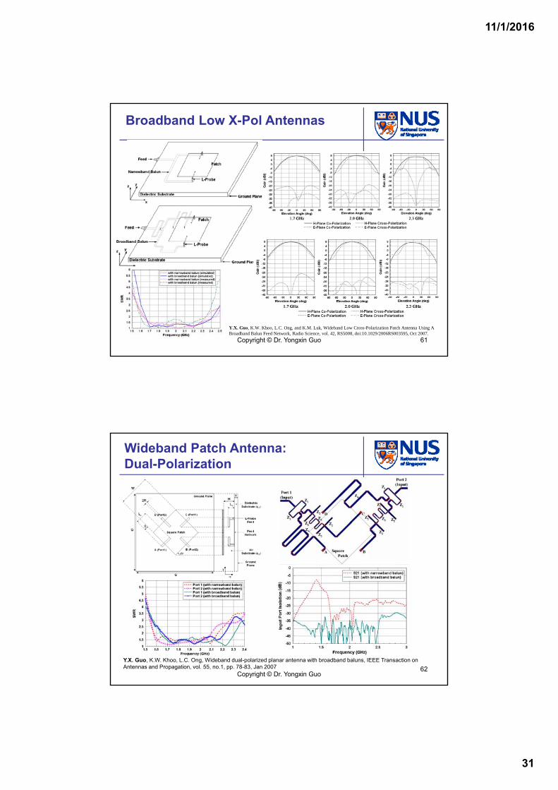
Broadband Low X-Pol Antennas
Y.X. Guo, K.W. Khoo, L.C. Ong, and K.M. Luk, Wideband Low Cross-Polarization Patch Antenna Using A Broadband Balun Feed Network, Radio Science, vol. 42, RS5008, doi:10.1029/2006RS003595, Oct 2007.
Copyright © Dr. Yongxin Guo 61
MMIC Modelling & Packaging Lab
Wideband Patch Antenna: Dual-Polarization
Y.X. Guo, K.W. Khoo, L.C. Ong, Wideband dual-polarized planar antenna with broadband baluns, IEEE Transaction on Antennas and Propagation, vol. 55, no.1, pp. 78-83, Jan 2007
Copyright © Dr. Yongxin Guo62
11/1/2016
32
MMIC Modelling & Packaging Lab
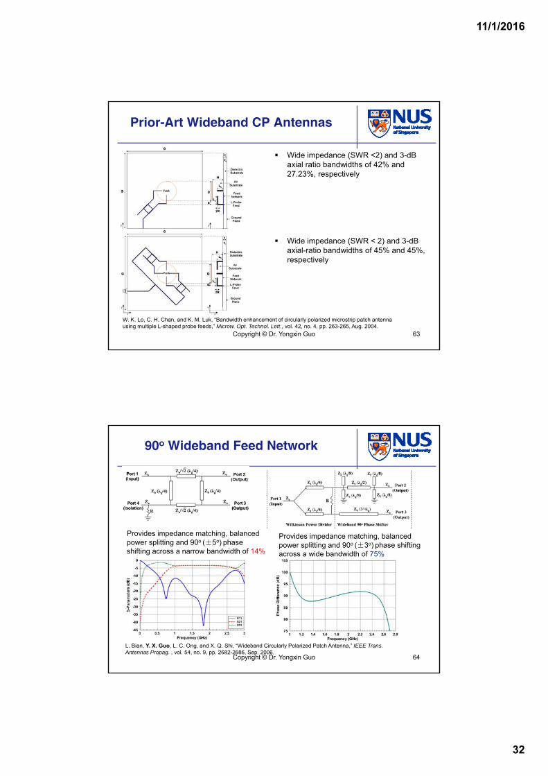
Wide impedance (SWR <2) and 3-dB axial ratio bandwidths of 42% and 27.23%, respectively
W. K. Lo, C. H. Chan, and K. M. Luk, “Bandwidth enhancement of circularly polarized microstrip patch antennausing multiple L-shaped probe feeds,” Microw. Opt. Technol. Lett., vol. 42, no. 4, pp. 263-265, Aug. 2004.
Wide impedance (SWR < 2) and 3-dB axial-ratio bandwidths of 45% and 45%, respectively
Prior-Art Wideband CP Antennas
Copyright © Dr. Yongxin Guo 63
MMIC Modelling & Packaging Lab
Provides impedance matching, balanced power splitting and 90o (±3o) phase shifting across a wide bandwidth of 75%
Provides impedance matching, balanced power splitting and 90o (±5o) phase shifting across a narrow bandwidth of 14%
L. Bian, Y. X. Guo, L. C. Ong, and X. Q. Shi, “Wideband Circularly Polarized Patch Antenna,” IEEE Trans. Antennas Propag. , vol. 54, no. 9, pp. 2682-2686, Sep. 2006.
90o Wideband Feed Network
Copyright © Dr. Yongxin Guo 64
11/1/2016
33
Wideband CP Patch Antenna:
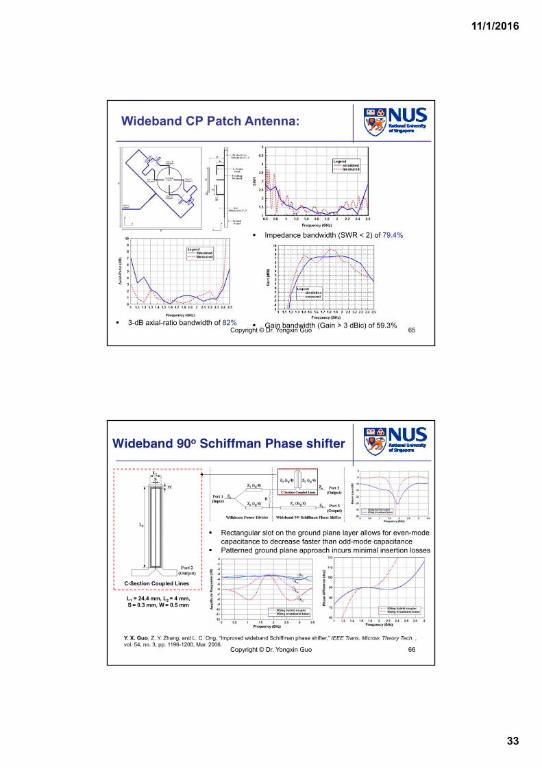
Impedance bandwidth (SWR < 2) of 79.4%
3-dB axial-ratio bandwidth of 82% Gain bandwidth (Gain > 3 dBic) of 59.3% Copyright © Dr. Yongxin Guo 65
MMIC Modelling & Packaging Lab
Wideband 90o Schiffman Phase shifter
Y. X. Guo, Z. Y. Zhang, and L. C. Ong, “Improved wideband Schiffman phase shifter,” IEEE Trans. Microw. Theory Tech. , vol. 54, no. 3, pp. 1196-1200, Mar. 2006.
Rectangular slot on the ground plane layer allows for even-mode capacitance to decrease faster than odd-mode capacitance
Patterned ground plane approach incurs minimal insertion losses
C-Section Coupled Lines
L1 = 24.4 mm, L2 = 4 mm, S = 0.3 mm, W = 0.5 mm
Copyright © Dr. Yongxin Guo 66
11/1/2016
34
Y.X. Guo, K.W. Khoo, L.C. Ong, Wideband Circularly-Polarized planar antenna with broadband baluns, IEEE Transaction on Antennas and Propagation, vol. 56, no.2, pp. 319-326, Feb 2008
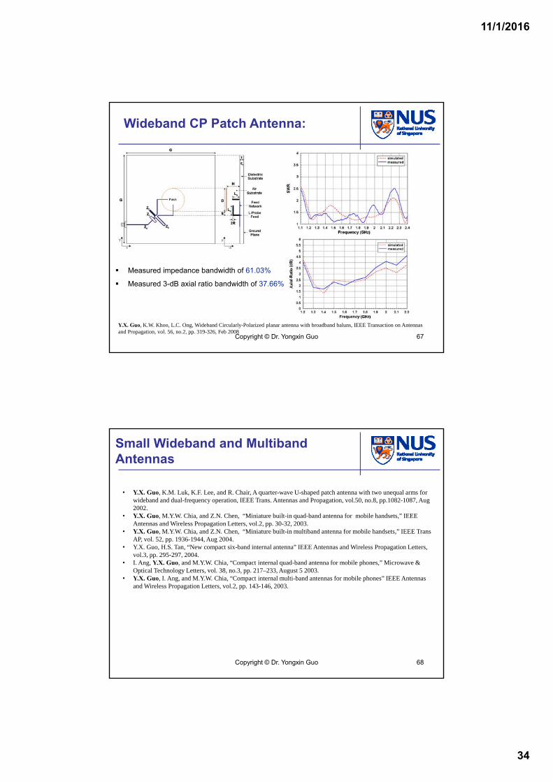
Measured impedance bandwidth of 61.03%
Measured 3-dB axial ratio bandwidth of 37.66%
Wideband CP Patch Antenna:
Copyright © Dr. Yongxin Guo 67
Small Wideband and Multiband Antennas
• Y.X. Guo, K.M. Luk, K.F. Lee, and R. Chair, A quarter-wave U-shaped patch antenna with two unequal arms for wideband and dual-frequency operation, IEEE Trans. Antennas and Propagation, vol.50, no.8, pp.1082-1087, Aug 2002.
• Y.X. Guo, M.Y.W. Chia, and Z.N. Chen, “Miniature built-in quad-band antenna for mobile handsets,” IEEE Antennas and Wireless Propagation Letters, vol.2, pp. 30-32, 2003.
• Y.X. Guo, M.Y.W. Chia, and Z.N. Chen, “Miniature built-in multiband antenna for mobile handsets,” IEEE Trans AP, vol. 52, pp. 1936-1944, Aug 2004.
• Y.X. Guo, H.S. Tan, “New compact six-band internal antenna” IEEE Antennas and Wireless Propagation Letters, vol.3, pp. 295-297, 2004.
• I. Ang, Y.X. Guo, and M.Y.W. Chia, “Compact internal quad-band antenna for mobile phones,” Microwave & Optical Technology Letters, vol. 38, no.3, pp. 217–233, August 5 2003.
• Y.X. Guo, I. Ang, and M.Y.W. Chia, “Compact internal multi-band antennas for mobile phones” IEEE Antennas and Wireless Propagation Letters, vol.2, pp. 143-146, 2003.
Copyright © Dr. Yongxin Guo 68
11/1/2016
35
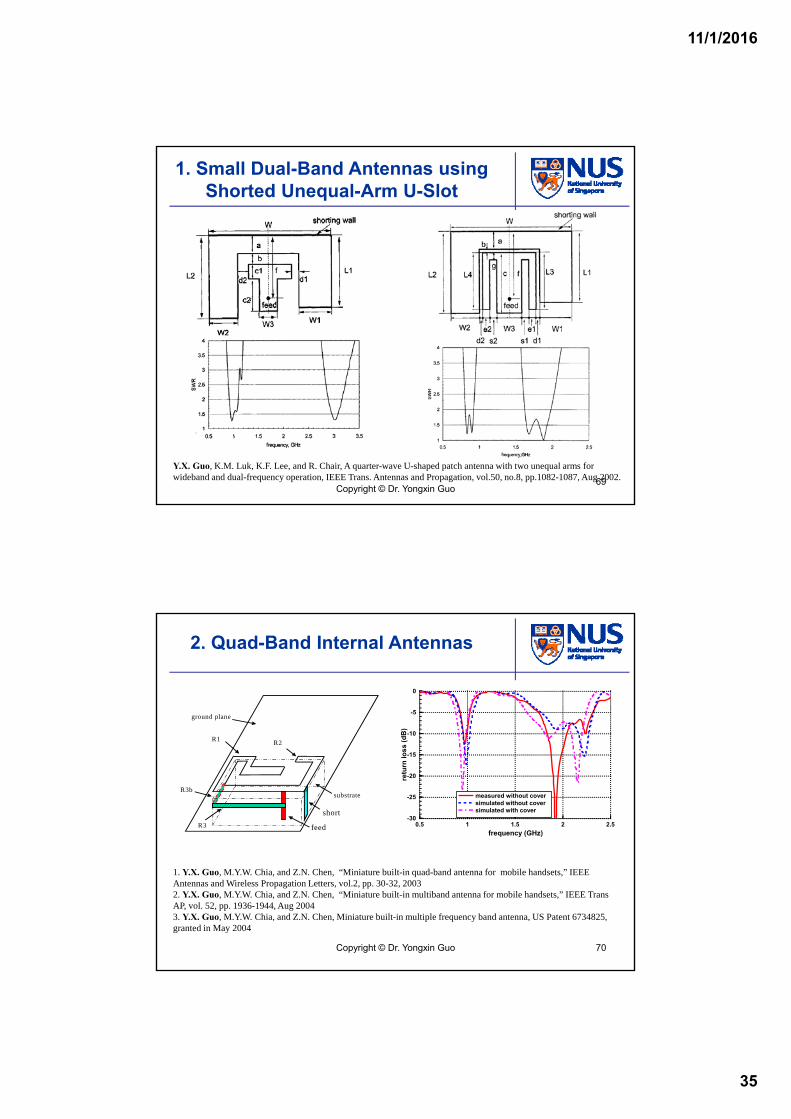
1. Small Dual-Band Antennas using Shorted Unequal-Arm U-Slot
Y.X. Guo, K.M. Luk, K.F. Lee, and R. Chair, A quarter-wave U-shaped patch antenna with two unequal arms for wideband and dual-frequency operation, IEEE Trans. Antennas and Propagation, vol.50, no.8, pp.1082-1087, Aug 2002.
Copyright © Dr. Yongxin Guo69
2. Quad-Band Internal Antennas
feed
short
R1 R2
ground plane
R3
R3bsubstrate
1. Y.X. Guo, M.Y.W. Chia, and Z.N. Chen, “Miniature built-in quad-band antenna for mobile handsets,” IEEE Antennas and Wireless Propagation Letters, vol.2, pp. 30-32, 20032. Y.X. Guo, M.Y.W. Chia, and Z.N. Chen, “Miniature built-in multiband antenna for mobile handsets,” IEEE Trans AP, vol. 52, pp. 1936-1944, Aug 20043. Y.X. Guo, M.Y.W. Chia, and Z.N. Chen, Miniature built-in multiple frequency band antenna, US Patent 6734825, granted in May 2004
0.5 1 1.5 2 2.5
frequency (GHz)
-30
-25
-20
-15
-10
-5
0
retu
rn lo
ss
(dB
)
measured without coversimulated without coversimulated with cover
Copyright © Dr. Yongxin Guo 70
11/1/2016
36
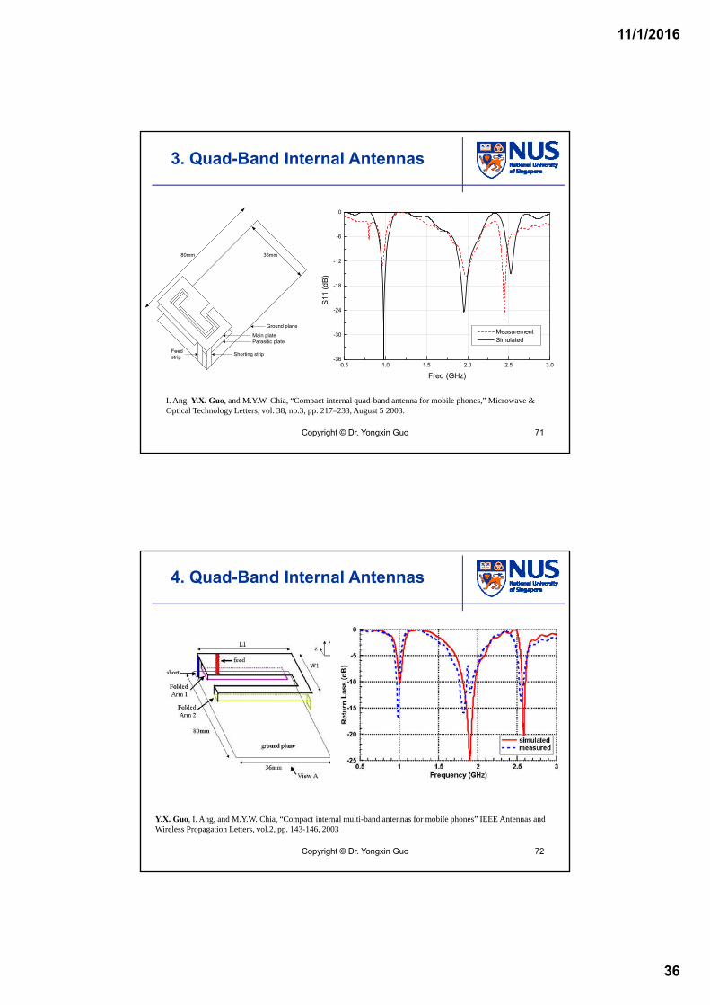
I. Ang, Y.X. Guo, and M.Y.W. Chia, “Compact internal quad-band antenna for mobile phones,” Microwave & Optical Technology Letters, vol. 38, no.3, pp. 217–233, August 5 2003.
Ground plane
Main plateParasitic plate
Shorting stripFeedstrip
36mm80mm
0.5 1.0 1.5 2.0 2.5 3.0-36
-30
-24
-18
-12
-6
0
Measurement Simulated
S11
(dB
)
Freq (GHz)
3. Quad-Band Internal Antennas
Copyright © Dr. Yongxin Guo 71
Y.X. Guo, I. Ang, and M.Y.W. Chia, “Compact internal multi-band antennas for mobile phones” IEEE Antennas and Wireless Propagation Letters, vol.2, pp. 143-146, 2003
4. Quad-Band Internal Antennas
Copyright © Dr. Yongxin Guo 72
11/1/2016
37
MMIC Modelling & Packaging Lab
Wideband Millimeter-Wave In-Package/On-Chip Antennas
1. K. Kang, F. Lin, D. Pham, J. Brinkhoff, C.H. Heng, Y.X. Guo, X.J. Yuan, A 42-mW 60-GHz OOK Receiver with an On-chip Antenna in 90nm CMOS, IEEE Journal of Solid-State Circuits (JSSC), Vol. 45, No. 9, pp. 1720-1731, Sept 2010.
2. M.F. Karim, Y.X. Guo, M. Sun, J. Brinkhoff, L.C. Ong, K. Kang, F. Lin, Integration of SiP Based 60GHz 4*4 Antenna Array with CMOS OOK Transmitter and LNA, IEEE Transactions on Microwave Theory and Technique, vol. 59, no.7, 2011, pp. 1869-1878
3. M. Sun, Y.Q. Zhang, Y.X. Guo, K. Faeyz, L.C. Ong, M.S. Leong, Integration of Circular Polarized Array and LNA in LTCC as a 60-GHz Active Receiving Antenna, IEEE Transactions on Antennas and Propagation, vol. 59, no. 8, pp. 3083-3089, Aug 2011.
4. C.R. Liu, Y.X. Guo, X.Y. Bao, S.Q. Xiao, 60-GHz LTCC Integrated Circularly Polarized Helical Antenna Array, IEEE Transactions on Antennas and Propagation, vol. 60, no.3, pp. 1329-1335, Mar 2012.
5. X.Y. Bao, Y.X. Guo, Y.Z. Xiong, 60-GHz AMC-Based Circularly Polarized On-Chip Antenna Using Standard 0.18-μm CMOS Technology, IEEE Transactions on Antennas and Propagation, vol. 60, no.5, pp. 2234-2241, May 2012.
6. H Chu , Y.X. Guo, et al, 135-GHz Micromachined On-chip Antenna and Antenna Array, IEEE Transactions on Antennas and Propagation, vol. 60, no. 10, pp. 4582-4588, Oct 2012.
7. H. Chu, Y.X. Guo, Z.L. Wang, 60-GHz LTCC Wideband Vertical Off-Center Dipole Antenna and Arrays, IEEE Transactions on Antennas and Propagation, vol. 61, no.1, pp. 153-161, Jan 2013.
8. H.C. Sun, Y.X. Guo, Z.L. Wang, 60-GHz Circularly Polarized U-Slot Patch Antenna Array on LTCC, IEEE Transactions on Antennas and Propagation, vol. 61, no.1, pp. 430-435, Jan 2013.
9. L. Wang, Y.X. Guo, W.X. Sheng, Wideband High-Gain 60-GHz LTCC L-Probe Patch Antenna Array with a Soft Surface, IEEE Transactions on Antennas and Propagation, vol. 61, no.4, pt1, pp. 1802-1809, Apr 2013.
10.Y.J. Cheng, X.Y. Bao, Y.X. Guo, 60-GHz LTCC Miniaturized Substrate Integrated Multibeam Array Antenna with Multiple Polarizations, IEEE Transactions on Antennas and Propagation. vol. 61, no.12, pp. 5958-5967, Dec 2013
11.Y.J. Cheng, Y.X. Guo, X.Y. Bao, K.B. Ng, Millimeter-Wave Low Temperature Co-Fired Ceramic Leaky-Wave Antenna and Array Based on the Substrate Integrated Image Guide Technology, IEEE Transactions on Antennas and Propagation, vol. 62, pp. 669-676, Feb 2014.
12.Y.J. Cheng, Y.X. Guo, Z.G. Liu, W-Band Large-Scale High-Gain Planar Integrated Antenna Array, IEEE Transactions on Antennas and Propagation, vol. 62, pp. 3370-3373, June 2014
Copyright © Dr. Yongxin Guo 73
Antennas in Package
On-Package Antenna solutions realize an antenna (or antennas) with highly-integrated radio die (or dies) into a standard surface mounted device symbolizing an innovative and important development in wireless frontier in recent years.
Copyright © Dr. Yongxin Guo 74

11/1/2016
38
Millimeter-wave and Sub-THz Radios
75
60 GHz
120 GHz
183 GHz 325 GHz
380 GHz
77/94 GHz
240 GHz
Source: T.S. Rappaport, et al, “State of the art in 60-GHz Integrated Circuits and Systems for Wireless Communications, “ Proceedings of IEEE, Aug 2011.
Copyright © Dr. Yongxin Guo
76
Why is Operation at 60 GHz Interesting
• License-free deployment
• Multi-gigabit operation
• Oxygen attenuates 60 GHz
signals
by 12-16 dB/km
• Immunity to interference
• Security from signal
interception Centralized base station
The intended range: 10 meters or less
• wireless replacement of cables Wireless Personal Area Networks
• high definition video streaming Wireless High-Definition Multimedia Interface (HDMI)
Copyright © Dr. Yongxin Guo
11/1/2016
39
Applications of 60-GHz Radios
Mobile Phones:Video download,bulk file transfer
PC & Peripherals:WUSB, Gaming
Consumer Electronics:HDTV, video streaming
Movie and Game Kiosk
77Copyright © Dr. Yongxin Guo
Wire-bonding Study at 60 GHz
WEST® BONDER Manual DIE/WIRE Bonder
78Copyright © Dr. Yongxin Guo
11/1/2016
40
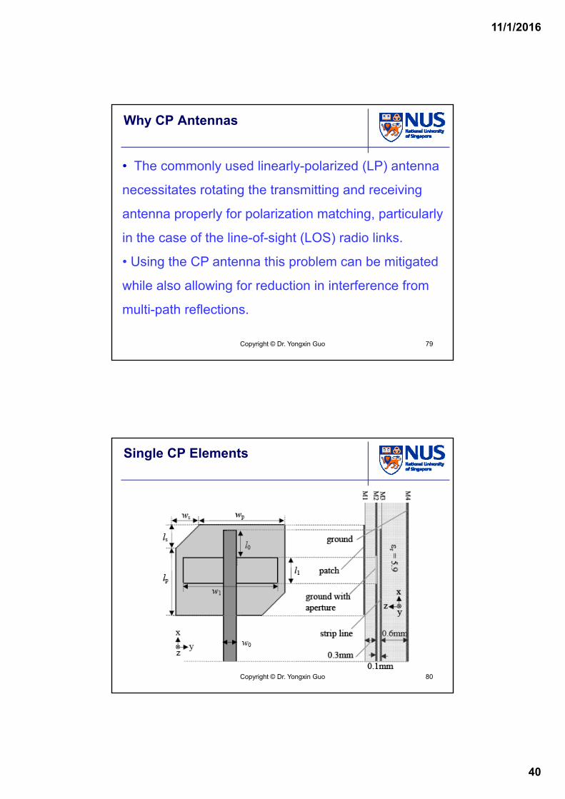
Why CP Antennas
79
• The commonly used linearly-polarized (LP) antenna
necessitates rotating the transmitting and receiving
antenna properly for polarization matching, particularly
in the case of the line-of-sight (LOS) radio links.
• Using the CP antenna this problem can be mitigated
while also allowing for reduction in interference from
multi-path reflections.
Copyright © Dr. Yongxin Guo
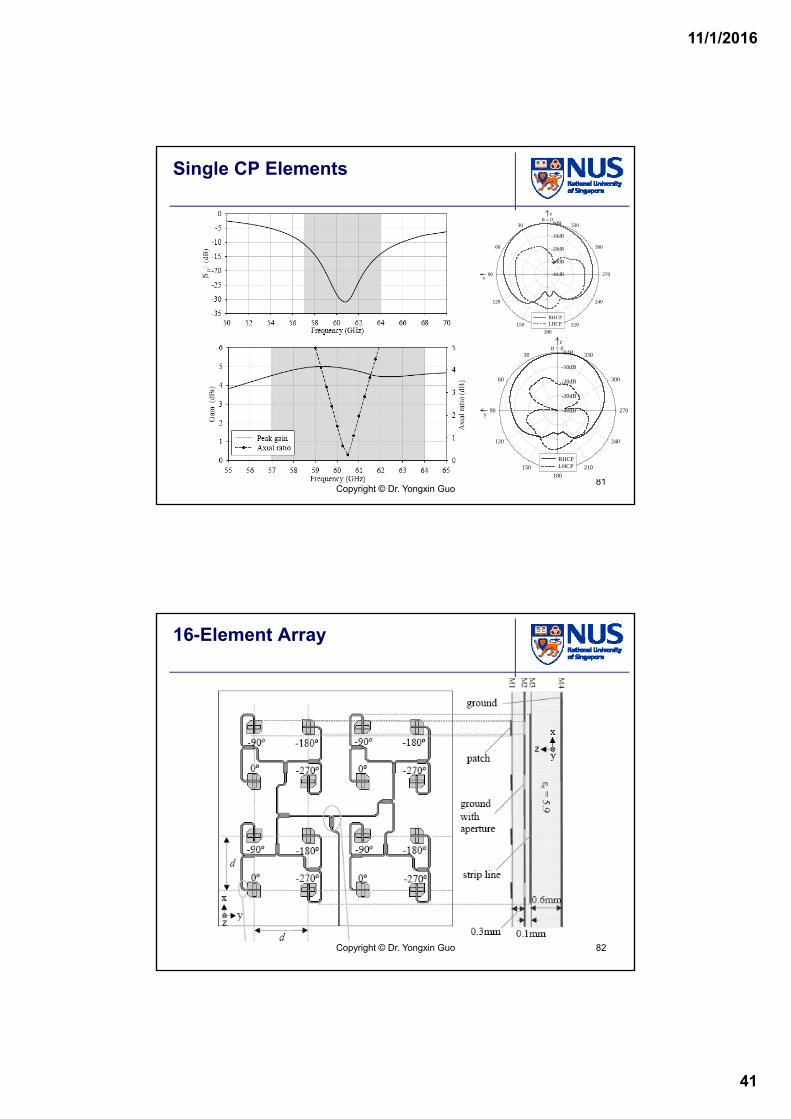
Single CP Elements
80Copyright © Dr. Yongxin Guo
11/1/2016
41
81
-40dB
-30dB
-20dB
-10dB
0dB0
30
60
90
120
150
180
210
240
270
300
330
RHCPLHCP
= 0z
x
-40dB
-30dB
-20dB
-10dB
0dB0
30
60
90
120
150
180
210
240
270
300
330
RHCPLHCP
= 0z
y
Single CP Elements
Copyright © Dr. Yongxin Guo
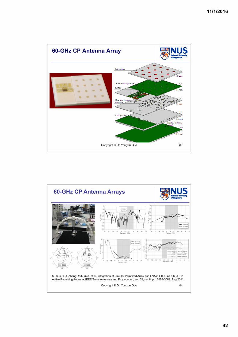
16-Element Array
82Copyright © Dr. Yongxin Guo
11/1/2016
42
60-GHz CP Antenna Array
83Copyright © Dr. Yongxin Guo
60-GHz CP Antenna Arrays
84
M. Sun, Y.Q. Zhang, Y.X. Guo, et al, Integration of Circular Polarized Array and LNA in LTCC as a 60-GHz Active Receiving Antenna, IEEE Trans Antennas and Propagation, vol. 59, no. 8, pp. 3083-3089, Aug 2011.
Copyright © Dr. Yongxin Guo

11/1/2016
43
60-GHz SiP Radios
85Copyright © Dr. Yongxin Guo
60-GHz SiP and System Test
Transmitted and recovered data using the OOK modulator and 4x4 antenna array with a data rate of 2Gb/s
86
M.F. Karim, Y.X. Guo, et al., Integration of SiP Based 60GHz 4*4 Antenna Array with CMOS OOK Transmitter and LNA, IEEE Trans MTT, vol. 59, no.7, 2011, pp. 1869-1878.
Copyright © Dr. Yongxin Guo
11/1/2016
44
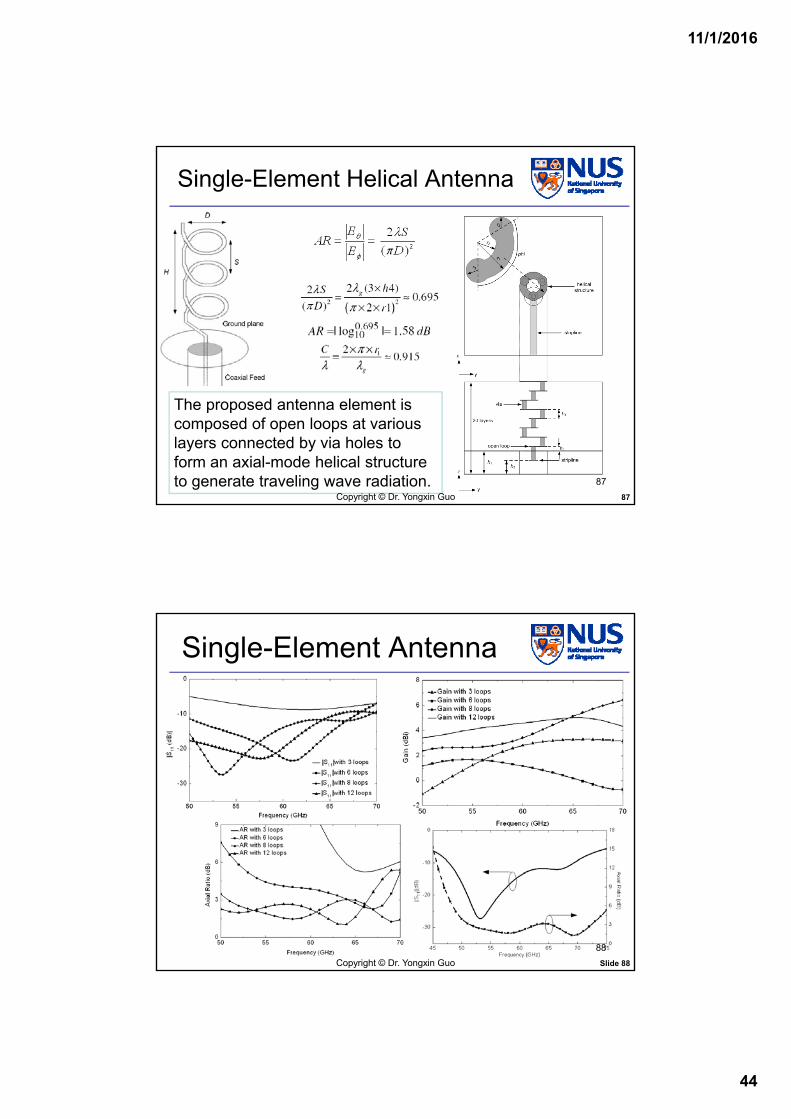
Single-Element Helical Antenna
87
The proposed antenna element is composed of open loops at various layers connected by via holes to form an axial-mode helical structure to generate traveling wave radiation.
Copyright © Dr. Yongxin Guo
87
Single-Element Antenna
Slide 88Copyright © Dr. Yongxin Guo
88

11/1/2016
45
Tolerance Study
Slide 89
40 50 60 70 80
-40
-30
-20
-10
0
r1=0.30mm, r
2=0.15mm,
r3=0.10mm
r1=0.31mm, r
2=0.14mm,
r3=0.11mm
r1=0.29mm, r
2=0.16mm,
r3=0.09mm
Frequency (GHz)
|S11
|(d
B)
40 50 60 70 80-40
-30
-20
-10
0
|S
11|(
dB
)
Frequency (GHz)
rvia
rvia+0.01mm
rvia-0.01mm
Shows the effect of the trace width variation. With a variation of ±0.01mm of r1, r2 and r3, the antenna performance can be kept almost unchanged in the bandwidth.
As for the misalignment of via holes, catch pads have been used to enhance the electrical connection. With a change of ±0.01mm of radius of via holes, the antenna impedance bandwidth is also kept almost unchanged.Copyright © Dr. Yongxin Guo
89
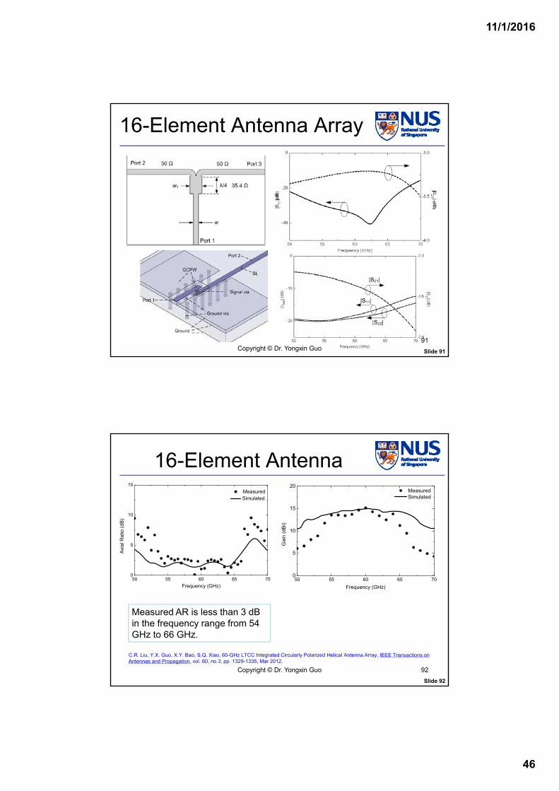
16-Element Antenna Array
Slide 90
50 55 60 65 70-40
-30
-20
-10
0
Frequency (GHz)
|S11
| (dB
)
Measured Simulated
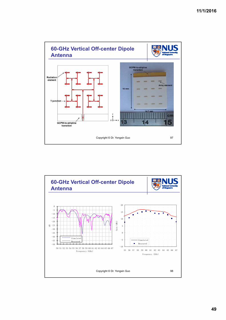
Composed of 16 antenna elements, T-junction feeding network and GCPW to stripline transition. Distance between neighboring elements is 2.5 mm and the size of this array is 12×10×2 mm3.
Measured |S11| is less than -10 dB in the frequency range from 52.5 GHz to 65.5 GHz.
Copyright © Dr. Yongxin Guo90
11/1/2016
46
16-Element Antenna Array
Slide 91Copyright © Dr. Yongxin Guo91
16-Element Antenna
Slide 92
50 55 60 65 700
5
10
15
Measured Simulated
Frequency (GHz)
Axi
al R
atio
(d
B)
50 55 60 65 700
5
10
15
20 Measured Simulated
Frequency (GHz)
Ga
in (
dB
i)
Measured AR is less than 3 dB in the frequency range from 54 GHz to 66 GHz.
C.R. Liu, Y.X. Guo, X.Y. Bao, S.Q. Xiao, 60-GHz LTCC Integrated Circularly Polarized Helical Antenna Array, IEEE Transactions on Antennas and Propagation, vol. 60, no.3, pp. 1329-1335, Mar 2012.
Copyright © Dr. Yongxin Guo 92

11/1/2016
47
16-Element Antenna
Slide 93
-40
-30
-20
-10
00
30
60
90
120
150180
210
240
270
300
330
40
30
20
10
0
Measured Simulated
-40
-30
-20
-10
00
30
60
90
120
150180
210
240
270
300
330
40
30
20
10
0
Measured Simulated
xz-plane
yz-plane
Copyright © Dr. Yongxin Guo 93
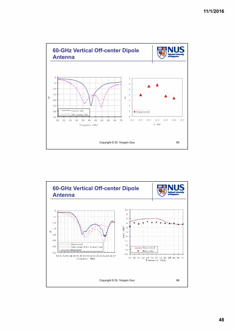
60-GHz Vertical Off-center Dipole Antenna
94
H. Chu, Y.X. Guo, Z.L. Wang, 60-GHz LTCC Wideband Vertical Off-Center Dipole Antenna and Arrays, IEEE Transactions on Antennas and Propagation, vol. 61, no.1, pp. 153-161, Jan 2013.
Copyright © Dr. Yongxin Guo
11/1/2016
48
60-GHz Vertical Off-center Dipole Antenna
95
-35
-30
-25
-20
-15
-10
-5
0
50 52 54 56 58 60 62 64 66 68 70
dB
Frequency (GHz)
Center-fed
Off-center fed0
1
2
3
4
5
6
7
0.1 0.2 0.3 0.4 0.5 0.6 0.7
h (mm)dBi
Simulated
Copyright © Dr. Yongxin Guo
60-GHz Vertical Off-center Dipole Antenna
96Copyright © Dr. Yongxin Guo
11/1/2016
49
60-GHz Vertical Off-center Dipole Antenna
97Copyright © Dr. Yongxin Guo
60-GHz Vertical Off-center Dipole Antenna
98
-50
-45
-40
-35
-30
-25
-20
-15
-10
-5
0
50 51 52 53 54 55 56 57 58 59 60 61 62 63 64 65 66 67
dB
Frequency (GHz)
Simulated
Measured
-10
-5
0
5
10
15
20
55 56 57 58 59 60 61 62 63 64 65 66 67
Frequency (GHz)
Gain (dBi)
Simulated
Measured
Copyright © Dr. Yongxin Guo
11/1/2016
50
60-GHz Vertical Off-center Dipole Antenna
99Copyright © Dr. Yongxin Guo
60-GHz Vertical Off-center Dipole Antenna
100
-50
-45
-40
-35
-30
-25
-20
-15
-10
-5
0
50 52 54 56 58 60 62 64 66 68 70
Frequency (GHz)
dB
|S11|
|S14|
|S22|
|S23|
|S13|
Copyright © Dr. Yongxin Guo

11/1/2016
51
60-GHz Vertical Off-center Dipole Antenna
101
-30
-25
-20
-15
-10
-5
0
-90 -80 -70 -60 -50 -40 -30 -20 -10 0 10 20 30 40 50 60 70 80 90
Angle (deg)
Norm
aliz
ed M
agnit
ude
(dB)
Port 1
Port 2
Port 3
Port 4-30
-25
-20
-15
-10
-5
0
-80 -70 -60 -50 -40 -30 -20 -10 0 10 20 30 40 50 60 70 80 90
Angle (dB)Normalized Magnitude (dB)
Port 1
Port 2
Port 3
Port 4
Simulated radiation pattern Measured radiation pattern
Copyright © Dr. Yongxin Guo
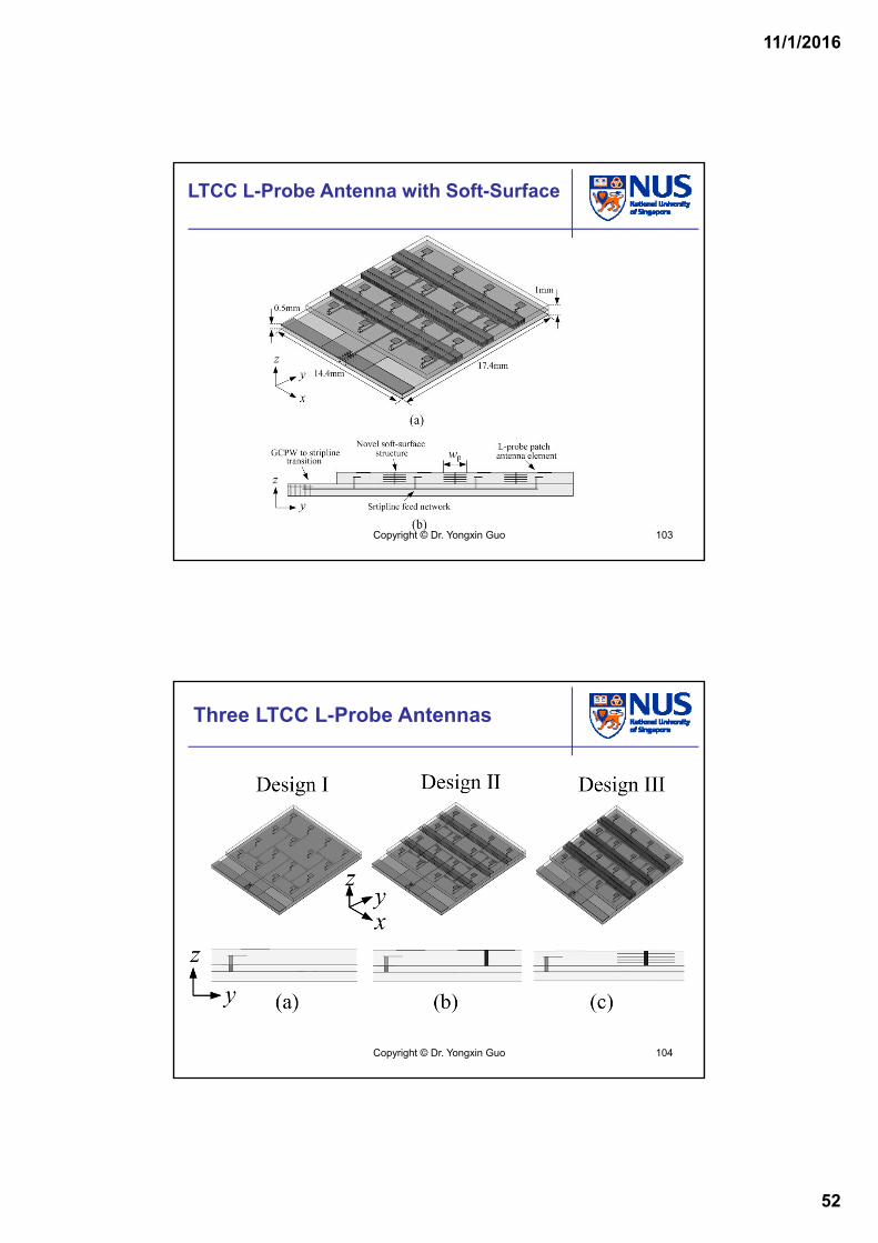
LTCC L-Probe Antenna
102
Para.Dimensions
(mm)Para.
Dimensions (mm)
w 0.7 l 0.7
w1 0.15 l1 0.25
w2 0.1 l2 0.4
h 1 h1 0.5
h2 0.3 h3 0.3
40 45 50 55 60 65 70 75 80-30
-25
-20
-15
-10
-5
0
-15
-10
-5
0
5
10
Copyright © Dr. Yongxin Guo
11/1/2016
52
103
LTCC L-Probe Antenna with Soft-Surface
Copyright © Dr. Yongxin Guo
104
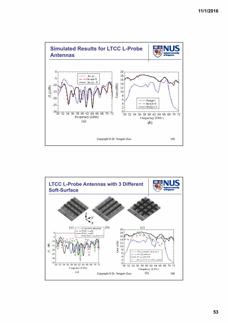
Three LTCC L-Probe Antennas
Copyright © Dr. Yongxin Guo
11/1/2016
53
105
50 52 54 56 58 60 62 64 66 68 70 72-30
-25
-20
-15
-10
-5
0
50 52 54 56 58 60 62 64 66 68 70 7202468
101214161820
Gai
n (d
Bi)
Simulated Results for LTCC L-Probe Antennas
Copyright © Dr. Yongxin Guo
106
50 52 54 56 58 60 62 64 66 68 70 72-35
-30
-25
-20
-15
-10
-5
0
50 52 54 56 58 60 62 64 66 68 70 7202468
101214161820
LTCC L-Probe Antennas with 3 Different Soft-Surface
Copyright © Dr. Yongxin Guo
11/1/2016
54
107
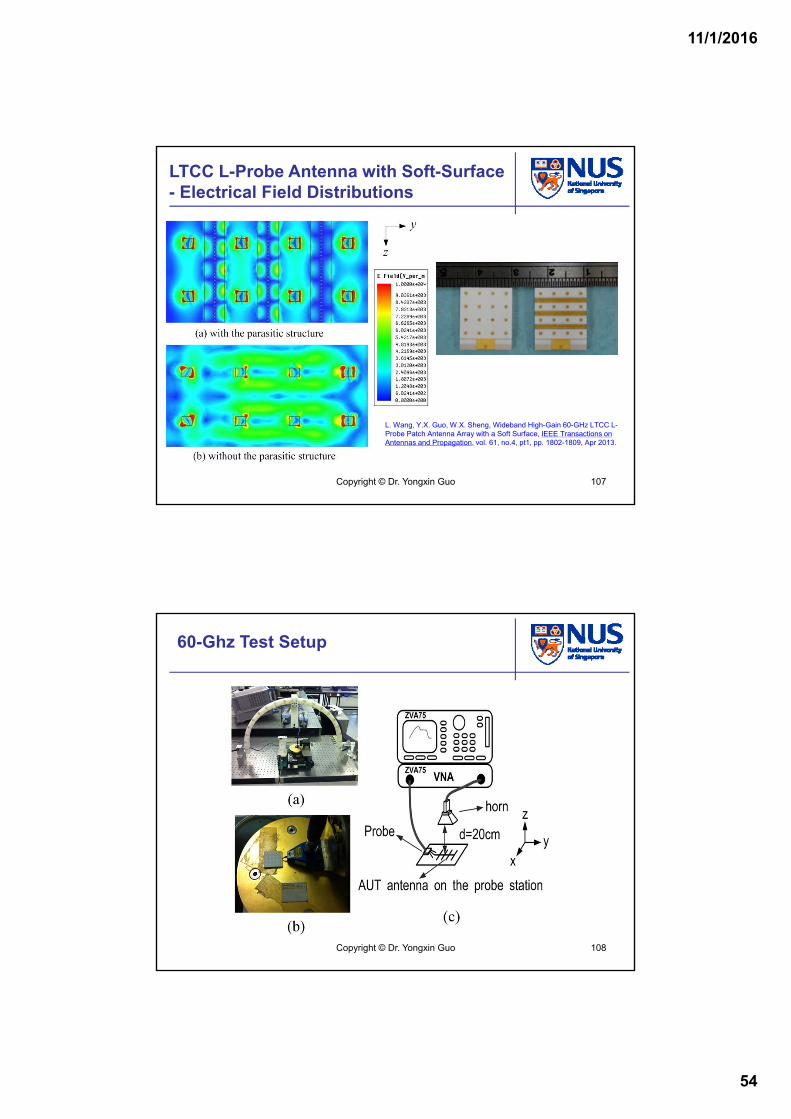
LTCC L-Probe Antenna with Soft-Surface- Electrical Field Distributions
L. Wang, Y.X. Guo, W.X. Sheng, Wideband High-Gain 60-GHz LTCC L-Probe Patch Antenna Array with a Soft Surface, IEEE Transactions on Antennas and Propagation, vol. 61, no.4, pt1, pp. 1802-1809, Apr 2013.
Copyright © Dr. Yongxin Guo
108
60-Ghz Test Setup
Copyright © Dr. Yongxin Guo
11/1/2016
55
109
50 52 54 56 58 60 62 64 66 68 70 72-35
-30
-25
-20
-15
-10
-5
0
Frequency (GHz)
|S11
| (dB
)
SimulatedMeasured
(a)
50 52 54 56 58 60 62 64 66 68 70 7202468
101214161820
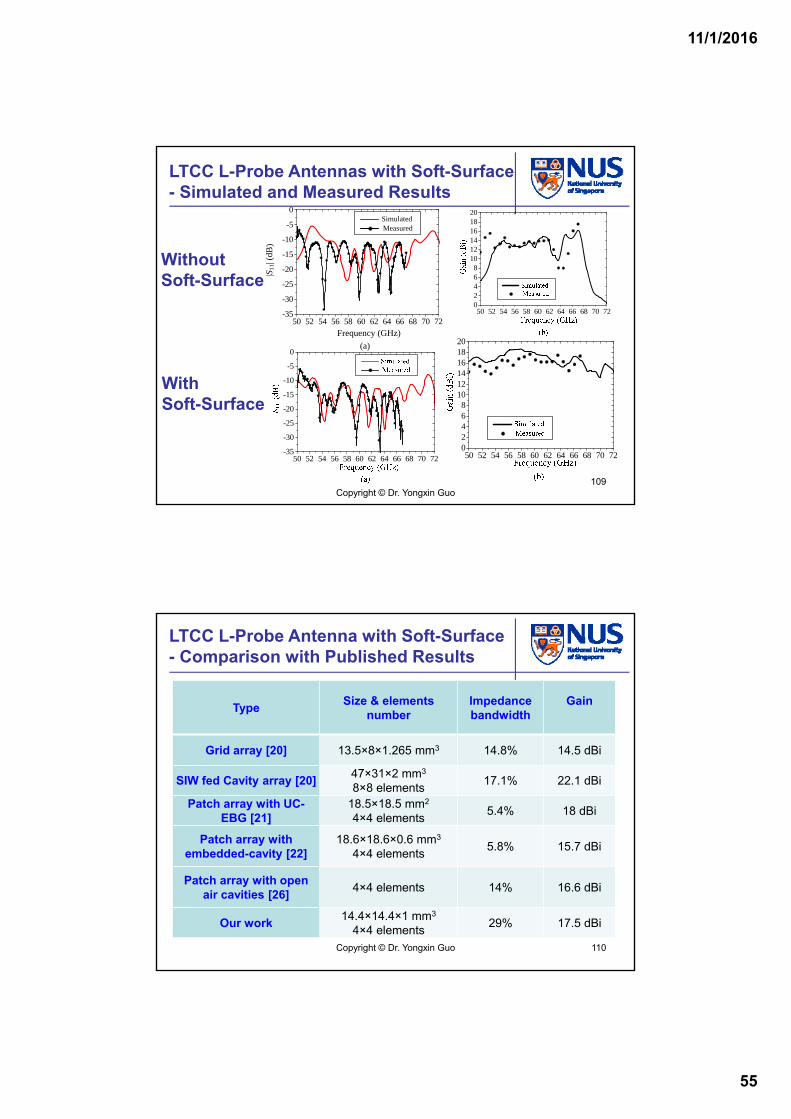
LTCC L-Probe Antennas with Soft-Surface- Simulated and Measured Results
50 52 54 56 58 60 62 64 66 68 70 72-35
-30
-25
-20
-15
-10
-5
0
50 52 54 56 58 60 62 64 66 68 70 7202468
101214161820
Without Soft-Surface
WithSoft-Surface
Copyright © Dr. Yongxin Guo
110
TypeSize & elements
numberImpedance bandwidth
Gain
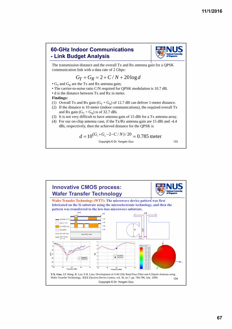
Grid array [20] 13.5×8×1.265 mm3 14.8% 14.5 dBi
SIW fed Cavity array [20]47×31×2 mm3
8×8 elements17.1% 22.1 dBi
Patch array with UC-EBG [21]
18.5×18.5 mm2
4×4 elements5.4% 18 dBi
Patch array with embedded-cavity [22]
18.6×18.6×0.6 mm3
4×4 elements5.8% 15.7 dBi
Patch array with open air cavities [26]
4×4 elements 14% 16.6 dBi
Our work14.4×14.4×1 mm3
4×4 elements29% 17.5 dBi
LTCC L-Probe Antenna with Soft-Surface- Comparison with Published Results
Copyright © Dr. Yongxin Guo
11/1/2016
56
111
-40
-30
-20
-10
00
30
60
90
120
150180
210
240
270
300
330
-40
-30
-20
-10
0
030
60
90
120
150180
210
240
270
300
330
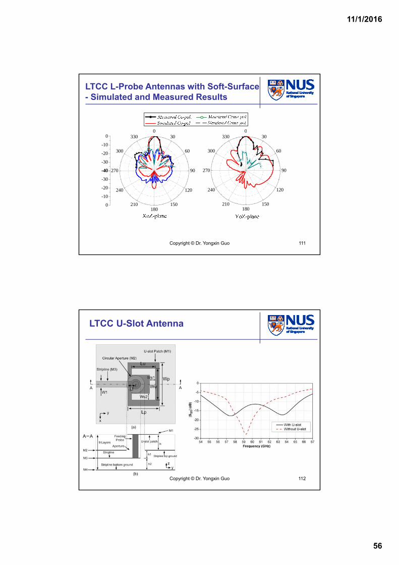
LTCC L-Probe Antennas with Soft-Surface- Simulated and Measured Results
Copyright © Dr. Yongxin Guo
LTCC U-Slot Antenna
112Copyright © Dr. Yongxin Guo
11/1/2016
57
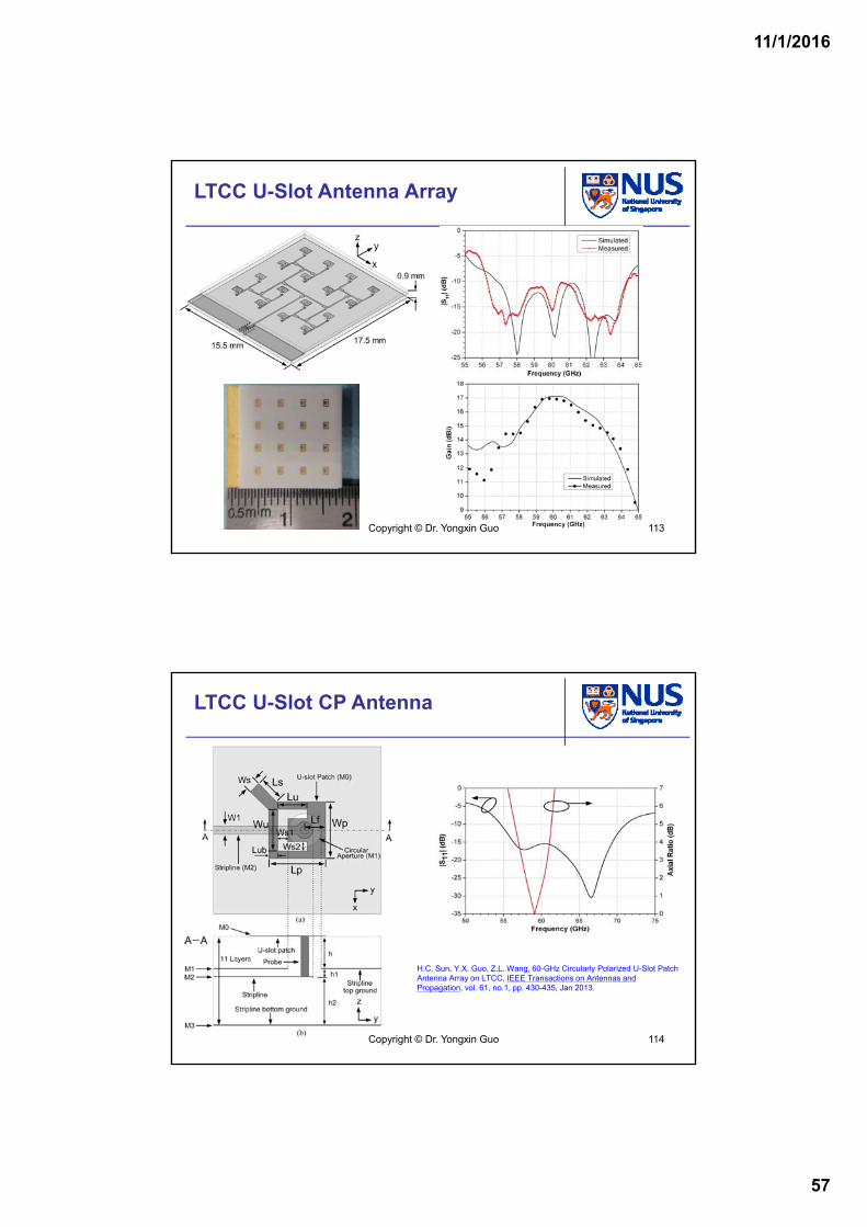
113
LTCC U-Slot Antenna Array
Copyright © Dr. Yongxin Guo
114
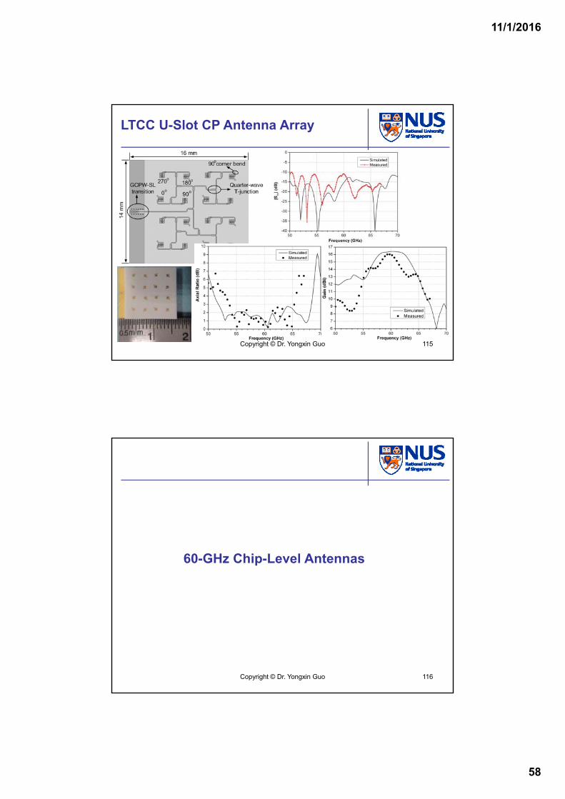
LTCC U-Slot CP Antenna
H.C. Sun, Y.X. Guo, Z.L. Wang, 60-GHz Circularly Polarized U-Slot Patch Antenna Array on LTCC, IEEE Transactions on Antennas and Propagation, vol. 61, no.1, pp. 430-435, Jan 2013.
Copyright © Dr. Yongxin Guo
11/1/2016
58
115
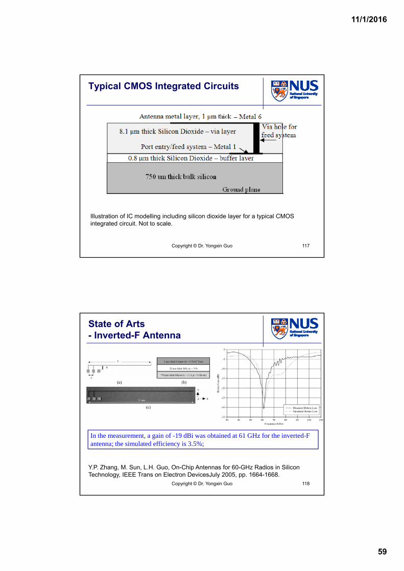
LTCC U-Slot CP Antenna Array
Copyright © Dr. Yongxin Guo
60-GHz Chip-Level Antennas
Copyright © Dr. Yongxin Guo 116
11/1/2016
59
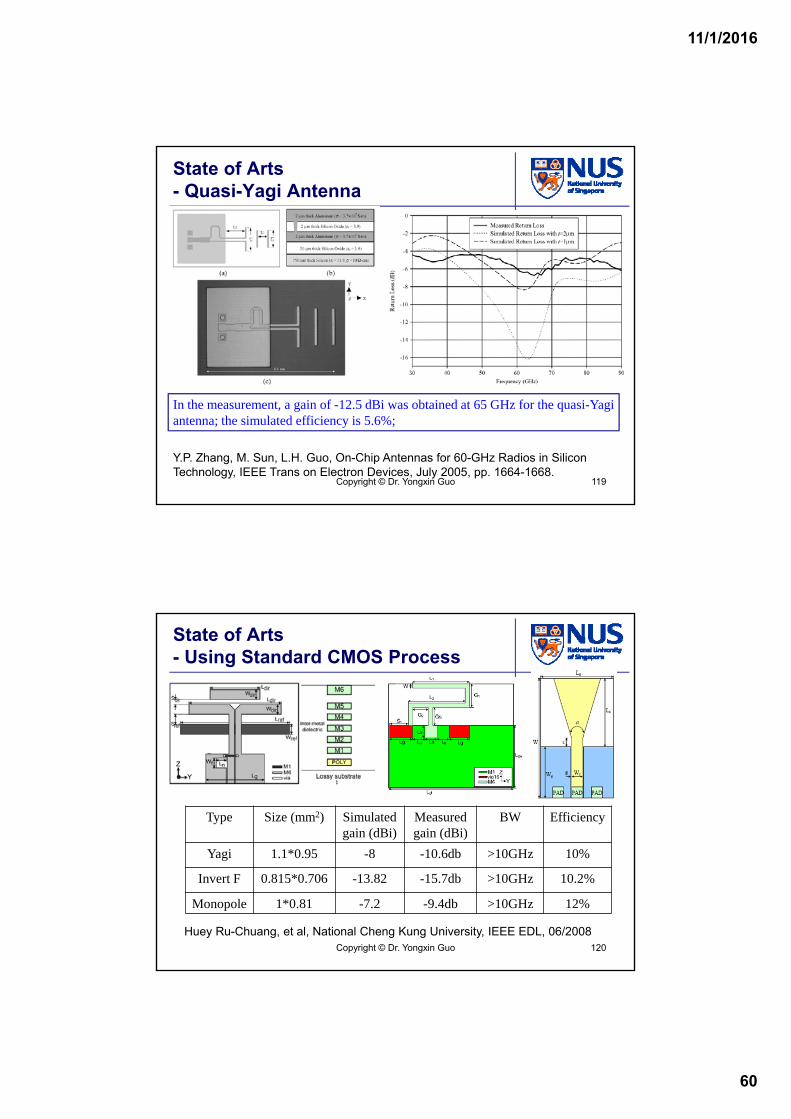
Illustration of IC modelling including silicon dioxide layer for a typical CMOS integrated circuit. Not to scale.
Typical CMOS Integrated Circuits
Copyright © Dr. Yongxin Guo 117
Y.P. Zhang, M. Sun, L.H. Guo, On-Chip Antennas for 60-GHz Radios in Silicon Technology, IEEE Trans on Electron DevicesJuly 2005, pp. 1664-1668.
State of Arts- Inverted-F Antenna
In the measurement, a gain of -19 dBi was obtained at 61 GHz for the inverted-F antenna; the simulated efficiency is 3.5%;
Copyright © Dr. Yongxin Guo 118
11/1/2016
60
Y.P. Zhang, M. Sun, L.H. Guo, On-Chip Antennas for 60-GHz Radios in Silicon Technology, IEEE Trans on Electron Devices, July 2005, pp. 1664-1668.
State of Arts- Quasi-Yagi Antenna
In the measurement, a gain of -12.5 dBi was obtained at 65 GHz for the quasi-Yagiantenna; the simulated efficiency is 5.6%;
Copyright © Dr. Yongxin Guo 119
State of Arts- Using Standard CMOS Process
120
Type Size (mm2) Simulated gain (dBi)
Measured gain (dBi)
BW Efficiency
Yagi 1.1*0.95 -8 -10.6db >10GHz 10%
Invert F 0.815*0.706 -13.82 -15.7db >10GHz 10.2%
Monopole 1*0.81 -7.2 -9.4db >10GHz 12%
Huey Ru-Chuang, et al, National Cheng Kung University, IEEE EDL, 06/2008 Copyright © Dr. Yongxin Guo

11/1/2016
61
60-GHz On-Chip Linearly Polarized Antennas
Copyright © Dr. Yongxin Guo 121
On-Chip Antennas using AMC
122
-150
-100
-50
0
50
100
150
200
50 52 54 56 58 60 62 64 66 68 70
Frequency (GHz)
Re
fle
cti
on
Ph
as
e (
de
g) sim.AMC.floquet port
sim.AMC.wave portsim.metal
Copyright © Dr. Yongxin Guo
11/1/2016
62
On-Chip Antennas using AMC- Current Distribution
123
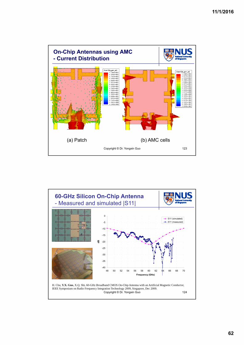
(a) Patch (b) AMC cells
Copyright © Dr. Yongxin Guo
60-GHz Silicon On-Chip Antenna- Measured and simulated |S11|
124
-40
-35
-30
-25
-20
-15
-10
-5
0
48 50 52 54 56 58 60 62 64 66 68 70
Frequency (GHz)
dB
S11 (simulated)
S11 (measured)
H. Chu, Y.X. Guo, X.Q. Shi, 60-GHz Broadband CMOS On-Chip Antenna with an Artificial Magnetic Conductor, IEEE Symposium on Radio Frequency Integration Technology 2009, Singapore, Dec 2009.
Copyright © Dr. Yongxin Guo
11/1/2016
63
60-GHz Silicon On-Chip Antenna- Measured and simulated gain
125
-10
-8
-6
-4
-2
0
2
4
50 52 54 56 58 60 62 64 66
Rad
iati
on
Gai
n (
dB
i)
Frequency (Ghz)
simulated gain
measured gain
Copyright © Dr. Yongxin Guo
60-GHz Silicon On-Chip Antenna- Radiation pattern at 60 GHz
126Copyright © Dr. Yongxin Guo
11/1/2016
64
60-GHz On-Chip Circularly Polarized Antennas
Copyright © Dr. Yongxin Guo 127
128
50 55 60 65 70 75 800
6
12
18
24
30
36
42
Full AMC Plane 4*4 AMC units blank 6*7 AMC units blank
Frequency (GHz)
Axi
al R
atio
(dB
)
50 55 60 65 70-20
-15
-10
-5
0
Full AMC 4*4 AMC units blank 6*7 AMC units blank W ithout AMC
Frequency (GHz)
Gai
n (
dBi)
60-GHz On-Chip CP Antenna- AR and gain comparison
X.Y. Bao, Y.X. Guo, Y.Z. Xiong, 60-GHz AMC-Based Circularly Polarized On-Chip Antenna Using Standard 0.18-μm CMOS Technology, IEEE Transactions on Antennas and Propagation, vol. 60, no.5, pp. 2234-2241, May 2012.
Copyright © Dr. Yongxin Guo
11/1/2016
65
60GHz On-Chip CP Antenna without AMC- Single and double loops comparison
129
50 55 60 65 70 750
3
6
9
12
15
18
21
Frequency (GHz)
Axi
al R
atio
(dB
)
Single Loop Double Loop
50 55 60 65 70-14
-12
-10
-8
-6 Single Loop Double Loop
Frequency (GHz)
Gai
n (d
Bi)
Copyright © Dr. Yongxin Guo
130
60-GHz On-Chip CP Antenna- AMC parametric study
d is the distance between elements
Lb
Copyright © Dr. Yongxin Guo
11/1/2016
66
60-GHz On-Chip CP Antenna- |S11|, AR and gain
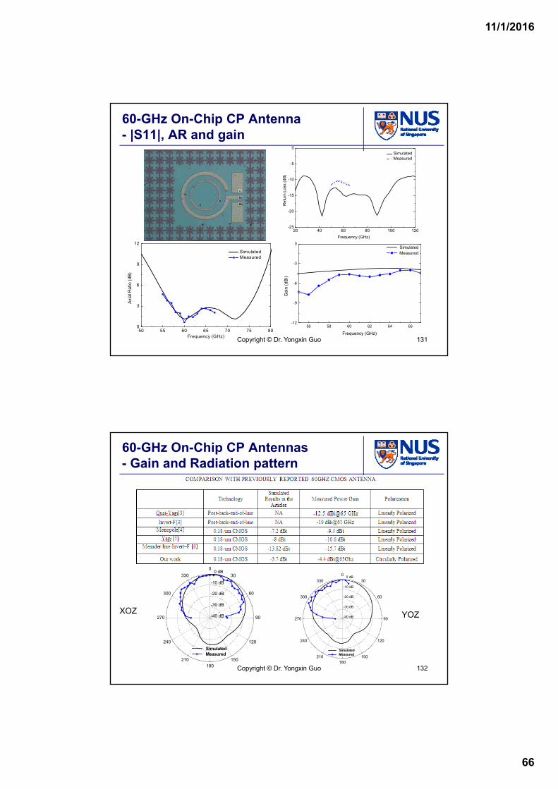
131
20 40 60 80 100 120-25
-20
-15
-10
-5
0 Simulated Measured
Frequency (GHz)
Ret
urn
Los
s (d
B)
56 58 60 62 64 66-12
-9
-6
-3
0 Simulated Measured
Frequency (GHz)
Gai
n (
dB
i)
50 55 60 65 70 75 800
3
6
9
12
Simulated Measured
Frequency (GHz)
Axi
al R
atio
(dB
)
Copyright © Dr. Yongxin Guo
60-GHz On-Chip CP Antennas- Gain and Radiation pattern
132
0
30
60
90
120
150180
210
240
270
300
330
Simulated Measured
0 dB
-20 dB
-10 dB
-30 dB
-40 dBXOZ
0
30
60
90
120
150180
210
240
270
300
330
Simulated Measured
0 dB
-20 dB
-10 dB
-30 dB
-40 dB YOZ
Copyright © Dr. Yongxin Guo
11/1/2016
67
60-GHz Indoor Communications- Link Budget Analysis
133
The transmission distance and the overall Tx and Rx antenna gain for a QPSK communication link with a data rate of 2 Gbps:
• GT and GR are the Tx and Rx antenna gain;• The carrier-to-noise ratio C/N required for QPSK modulation is 10.7 dB. • d is the distance between Tx and Rx in meter. Findings: (1) Overall Tx and Rx gain (GT + GR) of 12.7 dB can deliver 1-meter distance.(2) If the distance is 10 meter (indoor communications), the required overall Tx
and Rx gain (GT + GR) is of 32.7 dBi. (3) It is not very difficult to have antenna gain of 15 dBi for a Tx antenna array.(4) For our on-chip antenna case, if the Tx/Rx antenna gain are 15 dBi and -4.4
dBi, respectively, then the achieved distance for the QPSK is
dNCGG RT log20/2
meter 785.010 20/)/2( NCGGRTd
Copyright © Dr. Yongxin Guo
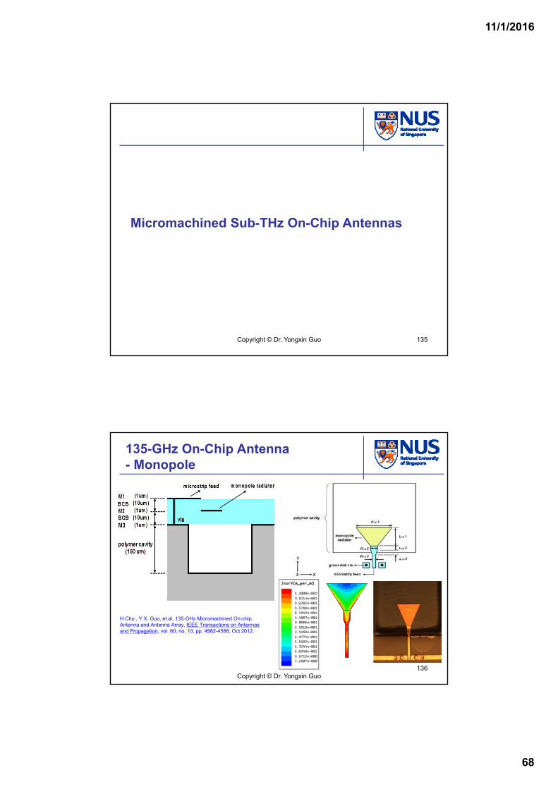
Innovative CMOS process: Wafer Transfer TechnologyWafer Transfer Technology (WTT): The microwave device pattern was first fabricated on the Si substrate using the microelectronic technology, and then the pattern was transferred to the low-loss microwave substrate.
Y.X. Guo, J.P. Wang, B. Luo, E.B. Liao, Development of A 60 GHz Band Pass Filter and A Dipole Antenna using Wafer Transfer Technology, IEEE Electron Device Letters, vol. 30, no.7, pp. 784-786, July 2009. 134
Copyright © Dr. Yongxin Guo
11/1/2016
68
Micromachined Sub-THz On-Chip Antennas
Copyright © Dr. Yongxin Guo 135
135-GHz On-Chip Antenna- Monopole
136
H Chu , Y.X. Guo, et al, 135-GHz Micromachined On-chip Antenna and Antenna Array, IEEE Transactions on Antennas and Propagation, vol. 60, no. 10, pp. 4582-4588, Oct 2012.
Copyright © Dr. Yongxin Guo
11/1/2016
69
135-GHz On-Chip Antenna- Fabrication process
137
3 main steps: 1) cavity fabrication, 2) polymer cavity filling 3) pattern formation through
back-end-of-line (BEOL) process; 2 redistribution layers (RDLs) are required.
Copyright © Dr. Yongxin Guo
135-GHz On-Chip monopole antenna- |S11|, gain and radiation pattern
138Copyright © Dr. Yongxin Guo
11/1/2016
70
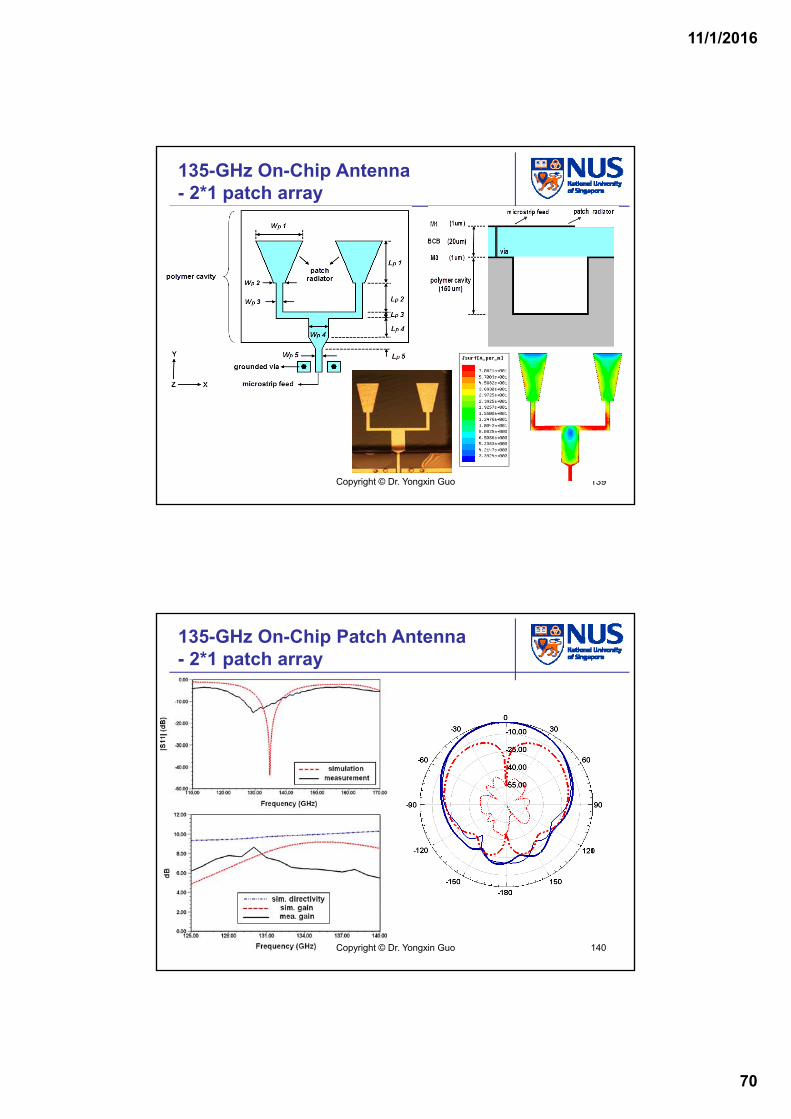
135-GHz On-Chip Antenna- 2*1 patch array
139Copyright © Dr. Yongxin Guo
135-GHz On-Chip Patch Antenna- 2*1 patch array
140Copyright © Dr. Yongxin Guo

11/1/2016
71
MMIC Modelling & Packaging Lab
1. Small Signal and large signal modeling2. High-power Ku-/Ka-band Power amplifier on GaAs/GaN3. 60/94 GHz power amplifier/LNA
• Z. Zhong, Y.X. Guo, M.S. Leong, A Consistent Charge Model of GaAs MESFETs for Ku-band Power Amplifiers, IEEE Transactions on Microwave Theory and Technique, vol. 59, no. 9, pp. 2246-2253, Sept 2011.
• Y.S. Long, Y.X. Guo, Z. Zhong, A 3-D Table-Based Method for Non-Quasi-Static Microwave FET Devices Modeling , IEEE Transactions on Microwave Theory and Techniques, vol. 60, no. 10, pp. 3088-3095, Oct 2012.
• X.J. Bi, Y.X. Guo, et al, “A 60 GHz 1 V-Supply Band-tunable Power Amplifier in 65 nm CMOS”, IEEE TRANSACTIONS ON CIRCUITS AND SYSTEMS II-EXPRESS BRIEFS,Volume: 58, Issue: 11,Pages: 719-723 NOV 2011.
• X.J. Bi, Y.X. Guo, Y.Z. Xiong, M.A. Arasu, M. Je, “A 19.2 mW, >45 dB gain and high-selectivity 94 GHz LNA in 0.13 um SiGe BiCMOS,” IEEE Wireless and Components Letters, vol. 23, no.5, pp. 261-263, May 2013
• X.J. Bi, Y.X. Guo, M. Je, Analysis and Design of Gain Enhanced Cascode Stage Utilizing a New Passive Compensation Network, IEEE Transactions on Microwave Theory and Techniques, vol. 61, no. 8, pp. 2892-2990, Aug 2013.
• K. Kang, F. Lin, D. Pham, J. Brinkhoff, C.H. Heng, Y.X. Guo, X.J. Yuan, A 42-mW 60-GHz OOK Receiver with an On-chip Antenna in 90nm CMOS, IEEE Journal of Solid-State Circuits (JSSC), Vol. 45, No. 9, pp. 1720-1731, Sept 2010.
• L. Wang, Y.X. Guo, Y. Lian, C.H. Heng, 3~5GHz 4-Channel UWB Beamforming Transmitter with 1° Phase Resolution through Calibrated Vernier Delay Line in 0.13μm CMOS, IEEE International Solid-State Circuits Conference 2012 (ISSCC2012), USA.
MMIC Modelling and Design
Copyright © Dr. Yongxin Guo141
0.18 um GaAs MESFETs Process Device Modelling
142Copyright © Dr. Yongxin Guo

11/1/2016
72
0.18 um GaAs MESFETs Wafer Device Small-signal Modelling
freq (1.000GHz to 40.00GHz)
Mea
sur
ed.S
(1,1
)S
imul
atio
n.S
(1,1
)
freq (1.000GHz to 40.00GHz)
Mea
sure
d.S
(1,2
)*1
5S
imu
latio
n.S
(1,2
)*15
Input Reflection Coefficient Reverse Transmission
freq (1.000GHz to 40.00GHz)
Mea
sure
d.S
(2,2
)S
imu
latio
n.S
(2,2
)
freq (1.000GHz to 40.00GHz)
Mea
sure
d.S
(2,1
)/15
Sim
ula
tion
.S(2
,1)/
15
Forward Transmission Output Reflection Coefficient
freq (1.000GHz to 40.00GHz)
Mea
sure
d.S
(1,1
)S
imul
atio
n.S
(1,1
)
freq (1.000GHz to 40.00GHz)
Mea
sure
d.S
(1,2
)*15
Sim
ula
tion
.S(1
,2)*
15
Input Reflection Coefficient Reverse Transmission
freq (1.000GHz to 40.00GHz)
Mea
su
red
.S(2
,2)
Sim
ula
tion
.S(2
,2)
freq (1.000GHz to 40.00GHz)
Mea
su
red
.S(2
,1)/
15
Sim
ula
tion
.S(2
,1)/
15
Forward Transmission Output Reflection Coefficient
8*150 um GaAs MESFET wafer deviceVgs = -0.3V, Vds = 7V, 1 – 40GHz
16*150 um GaAs MESFET wafer deviceVgs = -0.3V, Vds = 7V, 1 – 40GHz
143Copyright © Dr. Yongxin Guo
0.18 um GaAs MESFETs Wafer Device Large-signal Modelling
0 1 2 3 4 5 6 7 8 9 100
50
100
150
200
250
Vds
(V)
I ds
(mA
)
New modelMeasured data
0 1 2 3 4 5 6 7 8 9 100
100
200
300
400
500
600
700
Vds
(V)
I ds
(mA
)
New modelMeasured data
6×125 um GaAs MESFET wafer deviceVgs = -3.1 – 0.5V, Vds = 0 – 10V
16×125 um GaAs MESFET wafer deviceVgs = -3.1 – 0.5V, Vds = 0 – 10V
144
Z. Zhong, Y.X. Guo, M.S. Leong, A Consistent Charge Model of GaAs MESFETs for Ku-band Power Amplifiers, IEEE Transactions on Microwave Theory and Technique, vol. 59, no. 9, pp. 2246-2253, Sept 2011.
Copyright © Dr. Yongxin Guo
11/1/2016
73
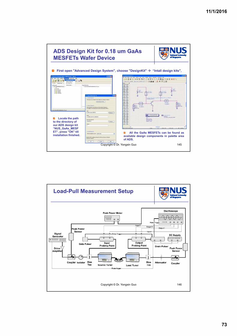
ADS Design Kit for 0.18 um GaAs MESFETs Wafer Device
Locate the path to the directory of our ADS design kit “NUS_GaAs_MESFET”, press "OK" till installation finished.
First open "Advanced Design System", choose "DesignKit" “Intall design kits",
All the GaAs MESFETs can be found asavailable design components in palette areaof ADS.
145Copyright © Dr. Yongxin Guo
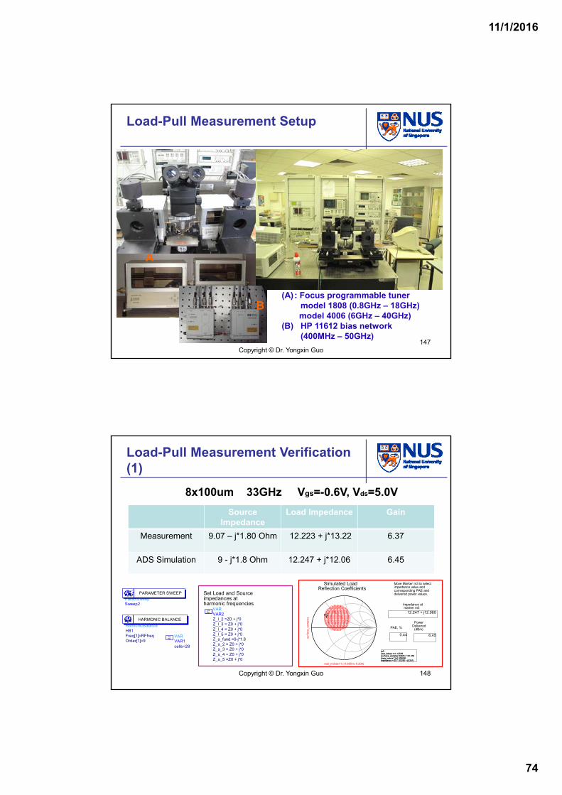
Load-Pull Measurement Setup
146Copyright © Dr. Yongxin Guo
11/1/2016
74
Load-Pull Measurement Setup
(A): Focus programmable tunermodel 1808 (0.8GHz – 18GHz)model 4006 (6GHz – 40GHz)
(B) HP 11612 bias network(400MHz – 50GHz)
A
B
147Copyright © Dr. Yongxin Guo
MMIC Modeling & Packaging Lab
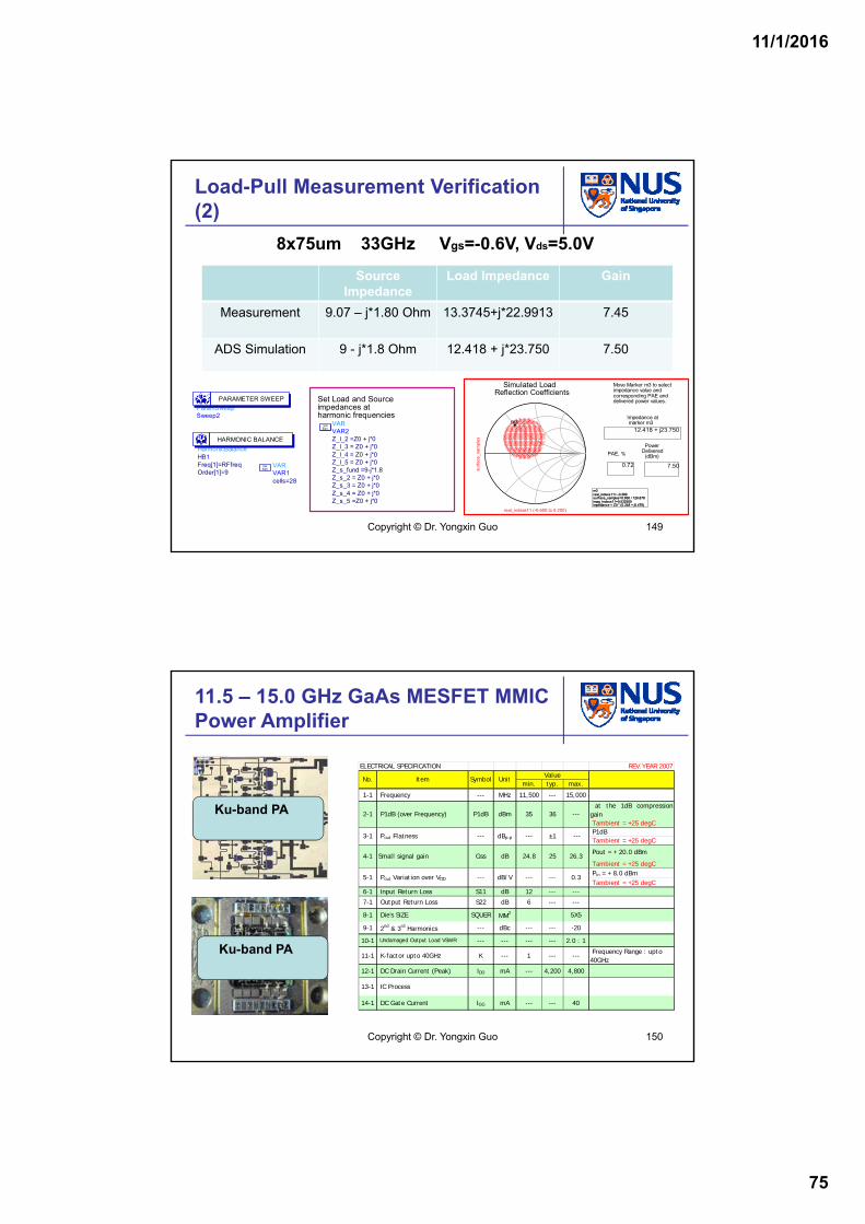
Load-Pull Measurement Verification (1)
8x100um 33GHz Vgs=-0.6V, Vds=5.0V
Source Impedance
Load Impedance Gain
Measurement 9.07 – j*1.80 Ohm 12.223 + j*13.22 6.37
ADS Simulation 9 - j*1.8 Ohm 12.247 + j*12.06 6.45
Set Load and Source impedances atharmonic frequencies
VARVAR2
Z_s_5 =Z0 + j*0Z_s_4 = Z0 + j*0Z_s_3 = Z0 + j*0Z_s_2 = Z0 + j*0Z_s_fund =9-j*1.8Z_l_5 = Z0 + j*0Z_l_4 = Z0 + j*0Z_l_3 = Z0 + j*0Z_l_2 =Z0 + j*0
EqnVar
VARVAR1cells=28
EqnVar
ParamSweepSweep2
PARAMETER SWEEP
HarmonicBalanceHB1
Order[1]=9Freq[1]=RFfreq
HARMONIC BALANCE
m3real_indexs11=surface_samples=0.625 / 151.319imag_indexs11=0.300000impedance = Z0 * (0.245 + j0.241)
-0.548
real_indexs11 (-0.600 to 0.200)
surf
ace
_sa
mp
les
m3
m3real_indexs11=surface_samples=0.625 / 151.319imag_indexs11=0.300000impedance = Z0 * (0.245 + j0.241)
-0.548
0.44
PAE, %
12.247 + j12.060
Impedance at marker m3
6.45
Power Delivered (dBm)
Move Marker m3 to select impedance value and corresponding PAE and delivered power values.
Simulated Load Reflection Coefficients
148Copyright © Dr. Yongxin Guo
11/1/2016
75
Load-Pull Measurement Verification (2)
8x75um 33GHz Vgs=-0.6V, Vds=5.0V
Source Impedance
Load Impedance Gain
Measurement 9.07 – j*1.80 Ohm 13.3745+j*22.9913 7.45
ADS Simulation 9 - j*1.8 Ohm 12.418 + j*23.750 7.50
Set Load and Source impedances atharmonic frequencies
VARVAR2
Z_s_5 =Z0 + j*0Z_s_4 = Z0 + j*0Z_s_3 = Z0 + j*0Z_s_2 = Z0 + j*0Z_s_fund =9-j*1.8Z_l_5 = Z0 + j*0Z_l_4 = Z0 + j*0Z_l_3 = Z0 + j*0Z_l_2 =Z0 + j*0
EqnVar
VARVAR1cells=28
EqnVar
ParamSweepSweep2
PARAMETER SWEEP
HarmonicBalanceHB1
Order[1]=9Freq[1]=RFfreq
HARMONIC BALANCE
m3real_indexs11=surface_samples=0.666 / 126.878imag_indexs11=0.532500impedance = Z0 * (0.248 + j0.475)
-0.399
real_indexs11 (-0.600 to 0.200)
surf
ace
_sa
mp
les
m3
m3real_indexs11=surface_samples=0.666 / 126.878imag_indexs11=0.532500impedance = Z0 * (0.248 + j0.475)
-0.399
0.72
PAE, %
12.418 + j23.750
Impedance at marker m3
7.50
Power Delivered (dBm)
Move Marker m3 to select impedance value and corresponding PAE and delivered power values.
Simulated Load Reflection Coefficients
149Copyright © Dr. Yongxin Guo
11.5 – 15.0 GHz GaAs MESFET MMIC Power Amplifier
ELECTRICAL SPECIFICATION REV.YEAR 2007Value
min. typ. max.
1-1 Frequency --- MHz 11,500 --- 15,000
at the 1dB compressiongain Tambient = +25 degC P1dB Tambient = +25 degC
Pout = + 20.0 dBm
Tambient = +25 degC Pin = + 8.0 dBm Tambient = +25 degC
6-1 Input Return Loss S11 dB 12 --- ---
7-1 Output Return Loss S22 dB 6 --- ---
8-1 Die's SIZE SQUER MM2 5X5
9-1 2nd & 3rd Harmonics --- dBc --- --- -20
10-1 Undamaged Output Load VSWR --- --- --- --- 2.0 : 1
11-1 K-factor upto 40GHz K --- 1 --- --- Frequency Range : upto 40GHz
12-1 DC Drain Current (Peak) IDD mA --- 4,200 4,800
13-1 IC Process
14-1 DC Gate Current IGG mA --- --- 40
--- 0.3
---
24.8 25 26.3
±1---
---5-1
3-1 Pout Flatness ---
4-1 Small signal gain Gss
2-1 P1dB dBm 35 36 ---
No. Item Symbol Unit
Pout Variation over VDD --- dB/V
P1dB (over Frequency)
dBp-p
dB
Ku-band PA
Ku-band PA
150Copyright © Dr. Yongxin Guo
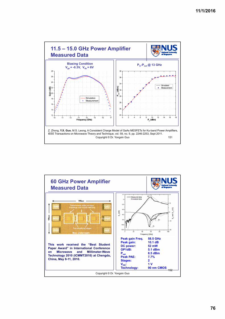
11/1/2016
76
11.5 – 15.0 GHz Power Amplifier Measured Data
0 2 4 6 8 10 12 14 16 1824
26
28
30
32
34
36
38
Po
ut (
dB
m)
Pin (dBm)
Simulated Measurement
10 11 12 13 14 15 16 1712
14
16
18
20
22
24
26
28
Simulation Measurement
Gai
n (
dB
)
Frequency (GHz)
Biasing ConditionVgs = -0.3V, Vds = 6V
Pin-Pout @ 13 GHz
151
Z. Zhong, Y.X. Guo, M.S. Leong, A Consistent Charge Model of GaAs MESFETs for Ku-band Power Amplifiers, IEEE Transactions on Microwave Theory and Technique, vol. 59, no. 9, pp. 2246-2253, Sept 2011.
Copyright © Dr. Yongxin Guo
60 GHz Power Amplifier Measured Data
Peak gain Freq. 58.5 GHzPeak gain: 10.1 dBDC power: 52 mWOP1dB: 5.1 dBmPsat 8.5 dBmPeak PAE: 7.7% Stages: 2 VDD: 1 V Technology: 90 nm CMOS
This work received the “Best StudentPaper Award” in International Conferenceon Microwave and Millimeter-WaveTechnology 2010 (ICMMT2010) at Chengdu,China, May 8-11, 2010.
Copyright © Dr. Yongxin Guo152
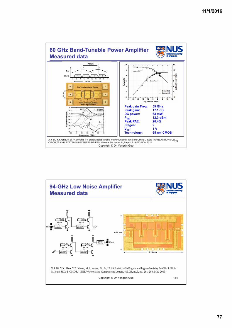
11/1/2016
77
Peak gain Freq. 59 GHzPeak gain: 17.1 dBDC power: 63 mWPsat 12.3 dBmPeak PAE: 20.4% Stages: 2 VDD: 1 V Technology: 65 nm CMOS
60 GHz Band-Tunable Power AmplifierMeasured data
X.J. Bi, Y.X. Guo, et al, “A 60 GHz 1 V-Supply Band-tunable Power Amplifier in 65 nm CMOS”, IEEE TRANSACTIONS ON CIRCUITS AND SYSTEMS II-EXPRESS BRIEFS, Volume: 58, Issue: 11,Pages: 719-723 NOV 2011.
Copyright © Dr. Yongxin Guo
153
94-GHz Low Noise AmplifierMeasured data
X.J. Bi, Y.X. Guo, Y.Z. Xiong, M.A. Arasu, M. Je, “A 19.2 mW, >45 dB gain and high-selectivity 94 GHz LNA in 0.13 um SiGe BiCMOS,” IEEE Wireless and Components Letters, vol. 23, no.5, pp. 261-263, May 2013
Copyright © Dr. Yongxin Guo 154
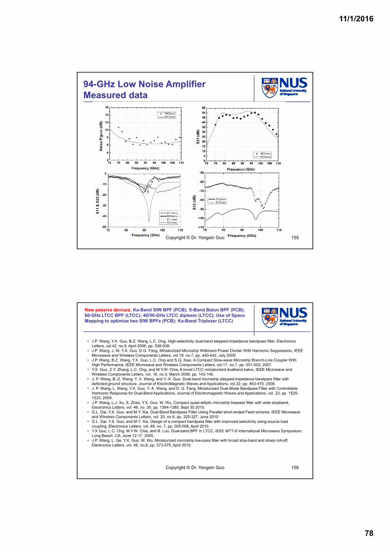
11/1/2016
78
94-GHz Low Noise AmplifierMeasured data
Copyright © Dr. Yongxin Guo 155
New passive devices: Ka-Band SIW BPF (PCB); X-Band Balun BPF (PCB); 60-GHz LTCC BPF (LTCC); 40/50-GHz LTCC diplexer (LTCC); Use of Space Mapping to optimize two SIW BPFs (PCB); Ka-Band Triplexer (LTCC)
• J.P. Wang, Y.X. Guo, B.Z. Wang, L.C. Ong, High-selectivity dual-band stepped-impedance bandpass filter, Electronics Letters, vol.42, no.9, April 2006, pp. 538-539.
• J.P. Wang, J. Ni, Y.X. Guo, D.G. Fang, Miniaturized Microstrip Wilkinson Power Divider With Harmonic Suppression, IEEE Microwave and Wireless Components Letters, vol.19, no.7, pp. 440-442, July 2009.
• J.P. Wang, B.Z. Wang, Y.X. Guo, L.C. Ong and S.Q. Xiao, A Compact Slow-wave Microstrip Branch-Line Coupler With High Performance, IEEE Microwave and Wireless Components Letters, vol.17, no.7, pp. 501-503, 2007.
• Y.X. Guo, Z.Y. Zhang, L.C. Ong, and M.Y.W. Chia, A novel LTCC miniaturized dualband balun, IEEE Microwave and Wireless Components Letters, vol. 16, no.3, March 2006, pp. 143-145.
• J. P. Wang, B.-Z. Wang, Y. X. Wang, and Y.-X. Guo, Dual-band microstrip stepped-impedance bandpass filter with defected ground structure, Journal of ElectroMagnetic Waves and Applications, vol.22, pp. 463-470, 2008.
• J. P. Wang, L. Wang, Y.X. Guo, Y.-X. Wang, and D. G. Fang, Miniaturized Dual-Mode Bandpass Filter with Controllable Harmonic Response for Dual-Band Applications, Journal of Electromagnetic Waves and Applications, vol. 23, pp. 1525-1533, 2009.
• J.P. Wang, L.J. Xu, S. Zhao, Y.X. Guo, W. Wu, Compact quasi-elliptic microstrip lowpass filter with wide stopband, Electronics Letters, vol. 46, no. 20, pp. 1384-1385, Sept 30 2010.
• G.L. Dai, Y.X. Guo, and M.Y. Xia, Dual-Band Bandpass Filter Using Parallel short-ended Feed scheme, IEEE Microwave and Wireless Components Letters, vol. 20, no.6, pp. 325-327, June 2010.
• G.L. Dai, Y.X. Guo, and M.Y. Xia, Design of a compact bandpass filter with improved selectivity using source-load coupling, Electronics Letters, vol. 46, no. 7, pp. 505-506, April 2010.
• Y.X Guo, L.C. Ong, M.Y.W. Chia, and B. Luo, Dual-band BPF in LTCC, IEEE MTT-S International Microwave Symposium, Long Beach, CA, June 12-17, 2005.
• J.P. Wang, L. Ge, Y.X. Guo, W. Wu, Miniaturized microstrip low-pass filter with broad stop-band and sharp roll-off, Electronics Letters, vol. 46, no.8, pp. 573-575, April 2010.
Copyright © Dr. Yongxin Guo 156
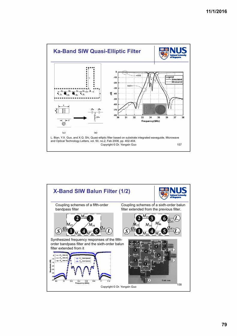
11/1/2016
79
Ka-Band SIW Quasi-Elliptic Filter
L. Bian, Y.X. Guo, and X.Q. Shi, Quasi-elliptic filter based on substrate integrated waveguide, Microwave and Optical Technology Letters, vol. 50, no.2, Feb 2008, pp. 402-404.
Copyright © Dr. Yongxin Guo 157
X-Band SIW Balun Filter (1/2)
Coupling schemes of a fifth-order bandpass filter
Coupling schemes of a sixth-order balun filter extended from the previous filter.
Synthesized frequency responses of the fifth-order bandpass filter and the sixth-order balun filter extended from it
Copyright © Dr. Yongxin Guo158
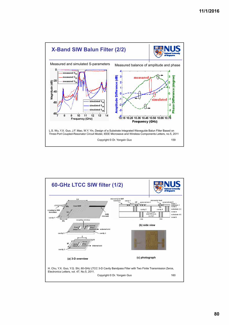
11/1/2016
80
X-Band SIW Balun Filter (2/2)
Measured and simulated S-parameters Measured balance of amplitude and phase
L.S. Wu, Y.X. Guo, J.F. Mao, W.Y. Yin, Design of a Substrate Integrated Waveguide Balun Filter Based on Three-Port Coupled-Resonator Circuit Model, IEEE Microwave and Wireless Components Letters, no.5, 2011
Copyright © Dr. Yongxin Guo 159
60-GHz LTCC SIW filter (1/2)
(a) 3-D overview
(b) side view
(c) photograph
H. Chu, Y.X. Guo, Y.Q. Shi, 60-GHz LTCC 3-D Cavity Bandpass Filter with Two Finite Transmission Zeros, Electronics Letters, vol. 47, No.5, 2011.
Copyright © Dr. Yongxin Guo 160
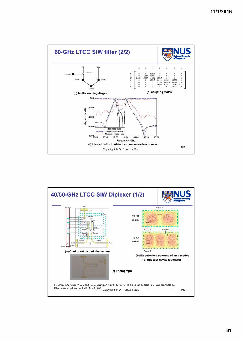
11/1/2016
81
60-GHz LTCC SIW filter (2/2)
(d) Multi-coupling diagram (e) coupling matrix
(f) Ideal circuit, simulated and measured responses
Copyright © Dr. Yongxin Guo161
40/50-GHz LTCC SIW Diplexer (1/2)
H. Chu, Y.X. Guo, Y.L. Song, Z.L. Wang, A novel 40/50 GHz diplexer design in LTCC technology,Electronics Letters, vol. 47, No.4, 2011.
(a) Configuration and dimensions
(b) Electric field patterns of and modes
in single SIW cavity resonator
(c) Photograph
Copyright © Dr. Yongxin Guo 162
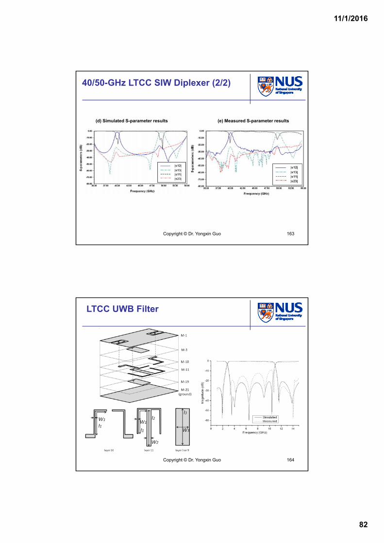
11/1/2016
82
40/50-GHz LTCC SIW Diplexer (2/2)
(d) Simulated S-parameter results (e) Measured S-parameter results
Copyright © Dr. Yongxin Guo 163
LTCC UWB Filter
Copyright © Dr. Yongxin Guo 164
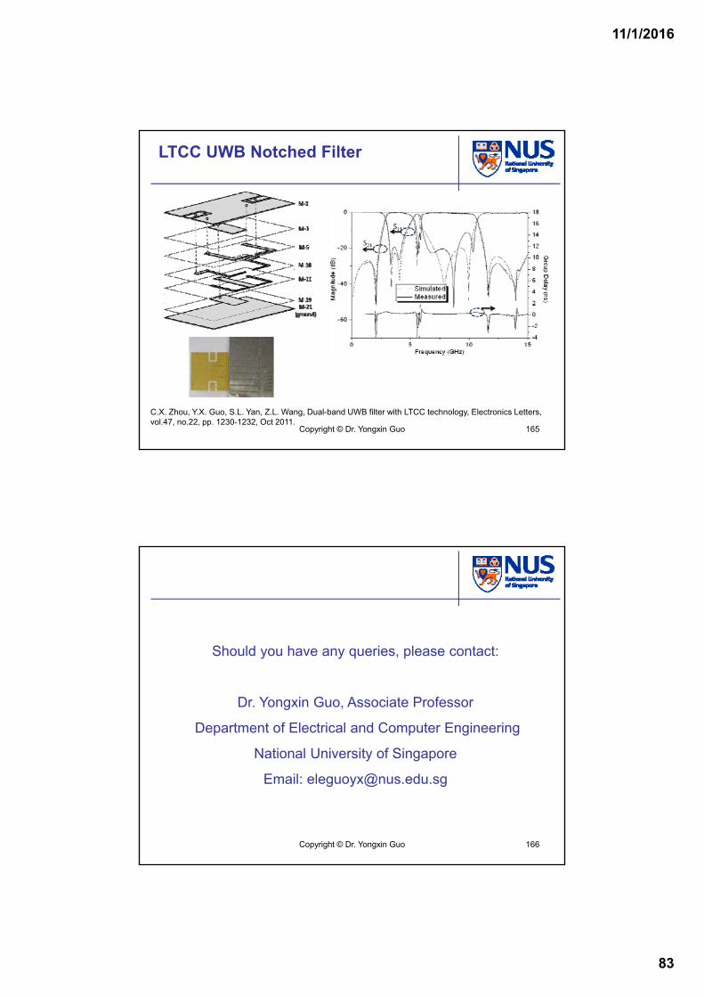
11/1/2016
83
LTCC UWB Notched Filter
C.X. Zhou, Y.X. Guo, S.L. Yan, Z.L. Wang, Dual-band UWB filter with LTCC technology, Electronics Letters, vol.47, no.22, pp. 1230-1232, Oct 2011.
Copyright © Dr. Yongxin Guo 165
Copyright © Dr. Yongxin Guo 166
Should you have any queries, please contact:
Dr. Yongxin Guo, Associate Professor
Department of Electrical and Computer Engineering
National University of Singapore
Email: [email protected]


![DESIGN AND ANALYSIS OF WIDEBAND PLANAR MONOPOLE ANTENNAS … · 2020. 1. 16. · planar monopole antennas have attracted many studies. Techniques such as adding shorting posts [10{12],](https://static.fdocuments.net/doc/165x107/60d5231b18413f5a56506387/design-and-analysis-of-wideband-planar-monopole-antennas-2020-1-16-planar-monopole.jpg)