S‑Ly ZO H H E H‑Perfor S‑Power Perovskit C Ptodetect O C
12
Vol.:(0123456789) 1 3 Single‑Layer ZnO Hollow Hemispheres Enable High‑Performance Self‑Powered Perovskite Photodetector for Optical Communication Xiyan Pan 1 , Jianqiang Zhang 1 , Hai Zhou 1 * , Ronghuan Liu 1 , Dingjun Wu 1 , Rui Wang 1 , Liangping Shen 1 , Li Tao 1 , Jun Zhang 1 , Hao Wang 1 * HIGHLIGHTS • Single-layer hollow ZnO hemispherical arrays behaving light trapping effect as the electron transport layer in perovskite photodetec- tors were first introduced. • Our photodetectors showed high self-powered performances with a LDR of 120.3 dB, a detectivity of 4.2 × 10 12 Jones, rise/fall time of 13/28 µs and the f −3 dB of up to 28 kHz. • Benefiting from the high device performance, the photodetector was demonstrated to the directional transmission of encrypted files as the signal receiving port with super high accuracy. ABSTRACT The carrier transport layer with reflection reduction morphology has attracted extensive attention for improving the utilization of light. Herein, we intro- duced single-layer hollow ZnO hemisphere arrays (ZHAs) behaving light trapping effect as the electron transport layer in perovskite photodetectors (PDs). The single- layer hollow ZHAs can not only reduce the reflection, but also widen the angle of the effective incident light and especially transfer the distribution of the optical field from the ZnO/FTO interface to the perovskite active layer confirmed by the 3D finite- difference time-domain simulation. These merits benefit for the generation, transport and separation of carriers, improving the light utilization efficiency. Finally, our opti- mized FTO/ZHA/CsPbBr 3 /carbon structure PDs showed high self-powered perfor- mance with a linear dynamic range of 120.3 dB, a detectivity of 4.2 × 10 12 Jones, rise/fall time of 13/28 µs and the f −3 dB of up to 28 kHz. Benefiting from the high device performance, the PD was demonstrated to the application in the directional transmission of encrypted files as the signal receiving port with super high accuracy. This work uniquely utilizes the features of high-performance self-powered perovskite PDs in optical communication, paving the path to wide applications of all-inorganic perovskite PDs. KEYWORDS Hemisphere array; Perovskite; Photodetector; Reflection reduction; Optical communication ISSN 2311-6706 e-ISSN 2150-5551 CN 31-2103/TB ARTICLE Cite as Nano-Micro Lett. (2021) 13:70 Received: 13 November 2020 Accepted: 29 December 2020 Published online: 12 February 2021 © The Author(s) 2021 https://doi.org/10.1007/s40820-021-00596-5 Xiyan Pan and Jianqiang Zhang contributed equally to this work. * Hai Zhou, [email protected]; Hao Wang, [email protected] 1 Hubei Key Laboratory of Ferro and Piezoelectric Materials and Devices, School of Microelectronics and Faculty of Physics and Electronic Science, Hubei University, Wuhan 430062, People’s Republic of China LED Signal Receiver Interpret file data and perform digital modulation Convert electrical signals into optical signals FPGA/LED Driver Glass FTO Carbon ZHA CsPbBr3
Transcript of S‑Ly ZO H H E H‑Perfor S‑Power Perovskit C Ptodetect O C

Vol.:(0123456789)
1 3
Single‑Layer ZnO Hollow Hemispheres Enable High‑Performance Self‑Powered Perovskite Photodetector for Optical Communication
Xiyan Pan1, Jianqiang Zhang1, Hai Zhou1 *, Ronghuan Liu1, Dingjun Wu1, Rui Wang1, Liangping Shen1, Li Tao1, Jun Zhang1, Hao Wang1 *
HIGHLIGHTS
• Single-layer hollow ZnO hemispherical arrays behaving light trapping effect as the electron transport layer in perovskite photodetec-tors were first introduced.
• Our photodetectors showed high self-powered performances with a LDR of 120.3 dB, a detectivity of 4.2 × 10¹² Jones, rise/fall time of 13/28 µs and the f−3 dB of up to 28 kHz.
• Benefiting from the high device performance, the photodetector was demonstrated to the directional transmission of encrypted files as the signal receiving port with super high accuracy.
ABSTRACT The carrier transport layer with reflection reduction morphology has attracted extensive attention for improving the utilization of light. Herein, we intro-duced single-layer hollow ZnO hemisphere arrays (ZHAs) behaving light trapping effect as the electron transport layer in perovskite photodetectors (PDs). The single-layer hollow ZHAs can not only reduce the reflection, but also widen the angle of the effective incident light and especially transfer the distribution of the optical field from the ZnO/FTO interface to the perovskite active layer confirmed by the 3D finite-difference time-domain simulation. These merits benefit for the generation, transport and separation of carriers, improving the light utilization efficiency. Finally, our opti-mized FTO/ZHA/CsPbBr3/carbon structure PDs showed high self-powered perfor-mance with a linear dynamic range of 120.3 dB, a detectivity of 4.2 × 10¹² Jones, rise/fall time of 13/28 µs and the f−3 dB of up to 28 kHz. Benefiting from the high device performance, the PD was demonstrated to the application in the directional transmission of encrypted files as the signal receiving port with super high accuracy. This work uniquely utilizes the features of high-performance self-powered perovskite PDs in optical communication, paving the path to wide applications of all-inorganic perovskite PDs.
KEYWORDS Hemisphere array; Perovskite; Photodetector; Reflection reduction; Optical communication
ISSN 2311-6706e-ISSN 2150-5551
CN 31-2103/TB
ARTICLE
Cite asNano-Micro Lett. (2021) 13:70
Received: 13 November 2020 Accepted: 29 December 2020 Published online: 12 February 2021 © The Author(s) 2021
https://doi.org/10.1007/s40820-021-00596-5
Xiyan Pan and Jianqiang Zhang contributed equally to this work. * Hai Zhou, [email protected]; Hao Wang, [email protected]
1 Hubei Key Laboratory of Ferro and Piezoelectric Materials and Devices, School of Microelectronics and Faculty of Physics and Electronic Science, Hubei University, Wuhan 430062, People’s Republic of China
LED
Signal Receiver
Interpret file data andperform digital modulation
Convert electrical signalsinto optical signals
FPGA/LED Driver
Glass
FTO
Carbon
ZHA
CsPbBr3

Nano-Micro Lett. (2021) 13:7070 Page 2 of 12
https://doi.org/10.1007/s40820-021-00596-5© The authors
1 Introduction
The advantages of the organic–inorganic hybrid halide per-ovskite, such as adjustable band gap, high optical absorption coefficient, long carrier diffusion length and carrier lifetime, high carrier mobility and low trap state density, enable the efficiency of the perovskite solar cells (SCs) climbing from 3.8% to 25.2% in the past decade [1–15]. However, due to the instability of organic cations, the commercialization of organic–inorganic halide perovskite optoelectronic devices is limited. Compared with organic halide perovskite, inor-ganic halide perovskite (CsPbX3, X = I, Br, Cl) has attracted more and more extensive attention on account of its better stability [16–29]. Self-powered photodetectors (PDs) based on all-inorganic halide perovskite can not only work at a low bias or even zero bias to obtain low-power devices, but also be easier to achieve higher detectivity due to the lower dark current, and these merits enable the self-powered PDs to be used in a wider field.
Conventionally, self-powered PDs are based on two kinds of structures, namely Schottky barrier type and PIN junc-tion type (or PN junction type). Compared with the former, the latter can greatly reduce the dark current of the device, enhance carrier transmission and inhabit carrier recombi-nation due to the existence of the carrier (electron/hole) transport layers, thereby improving the performances of the device (especially the switching ratio and detectivity) [30–36]. In addition, the carrier transport layer can effec-tively prevent the physical and chemical reaction between the electrode and the perovskite film, improving the device stability [37–42]. Moreover, the carrier transport layer with special morphology can effectively reduce the reflectivity of incident light and improve the utilization of light to enhance the device performances. Sargent’s team [43] found that the fully textured structure minimized reflection losses and improve the efficiency of light trapping, which was crucial to the device efficiency. Tian et al. [44] designed a nested inverse opal, which optimized the electron transport layer to enhance light capture, and the final device showed a high responsivity of 473 mA W−1 and the detectivity reaching 1.35 × 10¹³ Jones at 0 bias.
Herein, single-layer hollow ZnO hemisphere arrays (ZHAs) fabricated by using a polystyrene (PS) microsphere template were introduced to be the electron transport layer in perovskite PDs for enhancing light capture efficiency. In addition, compared with perovskite plane device, our
ZHA-based device can enable the main light field to be distributed in the perovskite, benefitting the generation and separation of the carriers. Finally, our FTO/ZHA/CsPbBr3/carbon structure self-powered PDs showed high perfor-mance with a linear dynamic range (LDR) of 120.3 dB, a detectivity of 4.2 × 10¹² Jones, rise/fall time of 13/28 µs and the f−3 dB of up to 28 kHz. Benefiting from the high device performance, the PD was applied to the directional trans-mission of encrypted files, in which the signal was sent by controlling the high-speed flashing of indoor light-emitting diodes (LEDs), and the PD as the signal receiving port con-verted the light into electrical signals, which were identified and transcoded from the controller through the field pro-grammable gate array (FPGA), thus realizing the directional transmission of files with super high accuracy.
2 Experimental Section
2.1 Device Fabrication
2.1.1 Single‑Layer ZHA Preparation
Ten-microliter ethanol dispersion of PS microspheres with a diameter of about 1 μm was dropped into a container filled with deionized water. When the dispersion was evenly dis-persed on the water surface, 1 mL of sodium dodecyl sulfate (SDS) aqueous solution (10 wt%) was dropped slowly from the edge of the container along the wall. After the SDS solu-tion driving the PS balls on the water surface to the other end to form a dense layer, the FTO substrate was inserted obliquely into the water, moved under the dense layer of PS microspheres and lifted slowly to transfer the PS balls to the substrate. Then the glass substrate with PS balls was dried on a hot stage at 60 ℃ for 30 min, and then, single-layer PS balls were obtained. After that, the single-layer PS ball/FTO substrate was sputtered with 200 nm ZnO and then placed in an annealing furnace at 500 ℃ for 1 h to obtain single-layer hollow ZHAs.
2.1.2 CsPb2Br5 Powder Preparation
PbBr2 (14.62 g, 40 mmol) was dissolved in 30 mL of aque-ous HBr (48%) solution and stirred to form a transpar-ent solution. Meanwhile, CsBr (4.26 mg, 20 mmol) was

Nano-Micro Lett. (2021) 13:70 Page 3 of 12 70
1 3
dissolved in 10 mL of H2O. When the two kinds of the solu-tion were mixed together, a white precipitate was formed immediately. The precipitate was filtered, then washed three times with anhydrous methanol and dried under vacuum. The CsPb2Br5 powder was obtained.
2.1.3 ZHA/CsPbBr3 Self‑Powered PD Preparation
1 mmol of CsPb2Br5 powder was dissolved in 1 mL of dimethyl sulfoxide (DMSO) (99.9%) and stirred for 12 h as the CsPb2Br5 precursor solution. The precursor solution was spin-coated on the ZHA/FTO substrate at a speed of 3000 rpm for 30 s and then annealed at 200 °C for 20 min. After that, 10 mg mL−1 CsBr/methanol (99%) solution was spin-coated at a speed of 3000 rpm for 40 s and annealed at 70 °C for 1 h. Then the carbon electrode was fabricated by doctor-blading process, and the ZHA/CsPbBr3 self-powered PDs were prepared.
2.2 Characterization
High-resolution scanning electron microscopy (SEM) images were recorded by field emission scanning electron microscopy (FESEM, JEOL, JSM-6700F), the X-ray diffrac-tion (XRD) pattern was carried out by using a D8 FOCUS X-ray diffractometer, and the absorption spectra were meas-ured by a UV–Vis spectrophotometer. The current–voltage (I–V) and current–time (I–t) curves were recorded by using a Keithley 2400 sourcemeter. An oscilloscope was used to characterize the fast response time of our devices. A 473-nm laser was used as the light source, and its optical power was calibrated by a standard Si diode. The photoluminescence (PL) spectrums and the time-resolved photoluminescence (TRPL) decay spectrums of the samples were measured by the time-correlated single-photon counting technique (Fluo-Time 300, Pico Quant GmbH).
2.3 Calculation
The simulation of light field distribution was performed by the Lumerical finite-difference time-domain (FDTD) soft-ware packages. The models of ZHA/CsPbBr3 and planar-ZnO/CsPbBr3 were determined according to the geometric parameters of real devices based on the SEM images; 550
and 473 nm plane waves were chosen as the light sources, and perfectly matched layer (PML) boundary conditions were adopted.
3 Results and Discussion
Figure 1 shows the preparation process of the ZHA/CsPbBr3 structure. Firstly, 10 μL of the ethanol dispersion of PS microspheres with a diameter of about 1 μm was dripped into a container filled with deionized water. When the dispersion was evenly dispersed on the water surface, 1 mL of sodium dodecyl sulfate (SDS) aqueous solu-tion (10 wt%) was used to drive the PS balls for obtain-ing a dense PS layer on the water surface. Then, the FTO substrate was used to pick up the PS microspheres and annealed at 60 °C for 30 min, and single-layer PS balls on the FTO substrate were obtained (Fig. S1a, c). After that, 200 nm ZnO was sputtered on the single-layer PS balls, following by annealing at 500 °C for 60 min to obtain a ZHA electron transport layer (Fig. S1b, d). To fabricate the ZHA/perovskite device, the CsPb2Br5 precursor solution was spin-coated on the ZHA electron transport layer due to its high solubility, and then the samples were soaked with CsBr methanol solution to obtain a high-quality CsPbBr3 light-absorbing layer [23]. The detailed experiment pro-cedures can be seen in the experimental part.
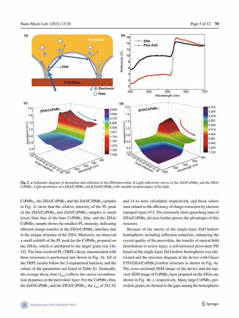
Figure 2a shows the light transmission process in the ZHA/CsPbBr3 thin film. As we known, when light is inci-dent from one medium to another, the light was reflected at the interfaces of layers which reduces the light utiliza-tion efficiency. Therefore, the traditional ZnO film, with-out light trapping structure, could loss a large amount of light due to the reflection (Fig. S2a). However, our ZHA layer with the hollow hemisphere structure can enable the reflection light to be refracted multiple times in the micro-cavity inside the film (Fig. 2a), which greatly reduces the light reflection (Fig. 2b), enhances the light absorption (Fig. S2b) and further effectively improves the light cap-ture efficiency. From the absorption spectrum, the absorp-tion edge of the perovskite was located at 530 nm, showing the band gap of 2.28 eV (Fig. S3). The relative transmit-tance (TR) of the ZnO and the ZHA can be calculated by the relative transmittance formula (Fig. S4), and the value of the TR was 26.85 and 4.26 for the ZHA and the ZnO,

Nano-Micro Lett. (2021) 13:7070 Page 4 of 12
https://doi.org/10.1007/s40820-021-00596-5© The authors
respectively. Therefore, these results further proved that the single-layer hollow ZnO hemisphere array structure was beneficial for the utilization of light due to the light trapping effect.
More importantly, our ZHA-based structure can enable the absorption of the perovskite behaving broader horizon compared with the traditional ZnO film-based structure, as shown in Fig. 2c, d and S5. With increasing the angle of the incident light, the absorption of planar ZnO/CsPbBr3 structure decreases sharply, while that of the ZHA-based device shows a negligible reduction, which is obviously attributed to the light trapping effect of the ZHA structure. Besides, when the incident angle of the light increases, the light absorption of planar devices will gradually decrease until it is all reflected. However, for the ZHA-based device, even if the incident angle of the light reaching 75°, the light absorption still can be up to 80% of the maximum value, showing that our ZHA-based perovskite PDs with superior light trapping capability and will benefit to the broad horizon.
The 3D FDTD simulation results of the light absorption distribution are shown in Fig. 3a and S6, S7, which displays that the light absorption of the planar device exhibits a lami-nar distribution because of the formation of standing wave [45]. The strongest light absorption (dark red part) is located
at the ZnO/FTO interface, which means great waste of light utilization. Interestingly, for the ZHA/perovskite device, the light field is mainly distributed in the perovskite active area, indicating that the distribution of the photogenerated carrier is transferred from the ZnO/FTO interface to the perovskite active layer, which benefits for the generation, transport and separation of carriers, improving the light utilization effi-ciency. Besides, the XRD patterns (Fig. 3b) show that the ZHA-based CsPbBr3 film behaves relatively higher intensity on the (100), (110) and (200) planes than that of the other two samples, indicating the ZnO hemisphere array structure could improve the crystallinity quality of the CsPbBr3 film due the big space between the hemispheres. This good crys-tallinity could result in much CsPb2Br5 precursor solution confined in the space and the high-quality CsPbBr3 film was formed [32]. Besides, from the peak intensity of the (100) plane, the grain size of the CsPbBr3 prepared on the ZHAs calculated according to the Scherrer formula D = Kλ/β cosθ (where D is the grain diameter along the direction perpen-dicular to the crystal plane, K is Scherrer constant, λ is the wavelength of incident X-ray, θ is Bragg diffraction angle, and β is the half-peak width of diffraction peak) is as large as 93.89 nm, which is almost 3 times of that of the ZnO/CsPbBr3 (33.5 nm) and the bare CsPbBr3 film (30.2 nm). The photoluminescence (PL) characterizations of the
Single layer PS ball
ZHA-CsPbBr3
CsPbBr
Picked up by FTO Annealing for 30 min at 60 °C
Annealing for 60 min at 500 °C
Annealing to dryness at 70 °C Annealing at 200 °C Spin coating CsPb2Br5Dropwise adding methanol/CsBr
Magnetron sputtering ZnO
Fig. 1 Preparation process of the ZHA/CsPbBr3 structure
Nano-Micro Lett. (2021) 13:70 Page 5 of 12 70
1 3
CsPbBr3, the ZHA/CsPbBr3 and the ZnO/CsPbBr3 samples in Fig. 3c show that the relative intensity of the PL peak of the ZHA/CsPbBr3 and ZnO/CsPbBr3 samples is much lower than that of the bare CsPbBr3 film, and the ZHA/CsPbBr3 sample shows the smallest PL intensity, indicating efficient charge transfer at the ZHA/CsPbBr3 interface due to the unique structure of the ZHA. Moreover, we observed a small redshift of the PL peak for the CsPbBr3 prepared on the ZHAs, which is attributed to the larger grain size [46, 54]. The time-resolved PL (TRPL) decay measurement with three structures is performed and shown in Fig. 3d. All of the TRPL results follow the 3-exponential function, and the values of the parameters are listed in Table S1. Generally, the average decay time (τave) reflects the carrier recombina-tion dynamics in the perovskite layer. For the CsPbBr3 film, the ZnO/CsPbBr3 and the ZHA/CsPbBr3, the τave of 283, 62
and 14 ns were calculated, respectively, and those values were related to the efficiency of charge extraction by electron transport layer [47]. The extremely short quenching time of ZHA/CsPbBr3 devices further proves the advantages of this structure.
Because of the merits of the single-layer ZnO hollow hemispheres including reflection reduction, enhancing the crystal quality of the perovskite, the transfer of optical field distribution to active layer, a self-powered perovskite PD based on the single-layer ZnO hollow hemispheres was fab-ricated and the structure diagram of the device with Glass/FTO/ZHA/CsPbBr3/carbon structure is shown in Fig. 4a. The cross-sectional SEM image of the device and the top-view SEM image of CsPbBr3 layer prepared on the ZHAs are shown in Fig. 4b, c, respectively. Many large CsPbBr3 per-ovskite grains are formed in the gaps among the hemispheres
Ref
lect
ivity
(%)
16
14
12
10
8
6
4
2
0
(b)(a)
(d)(c)
Electronic
ZHA
FTO/Glass
Perovskite
Hole
ZHA/CsPbBr3 ZnO/CsPbBr3
ZHAPlan ZnO
300 400 500 600 700Wavelength (nm)
1.6
1.4
1.2
1.0
0.8
0.6
0.40.2
−10 010203040 50
6070
80 650600
550
Wavelength (nm)Angle (degrees)
500450
Abs
orba
nce
(a.u
.)
1.6
1.4
1.2
1.0
0.8
0.6
0.40.2
−10 010203040506070
80 650
0.6060.6890.7720.8550.9381.0211.1041.1871.2701.3531.436
0.3140.3950.4760.5570.6380.7190.8000.8810.9621.0431.124
600550
Wavelength (nm)Angle (degrees)
500450
Abs
orba
nce
(a.u
.)
Fig. 2 a Schematic diagram of absorption and reflection of the ZHA/perovskite. b Light reflectivity curves of the ZnO/CsPbBr3 and the ZHA/CsPbBr3. Light absorbance of c ZHA/CsPbBr3 and d ZnO/CsPbBr3 with variable incident angles of the light

Nano-Micro Lett. (2021) 13:7070 Page 6 of 12
https://doi.org/10.1007/s40820-021-00596-5© The authors
and a largest perovskite grain is on top, leading to a smooth surface of the perovskite (Fig. S8), which benefits for the device performance and the stability.
Figure 4d shows the current density–voltage (J–V) curves of the device under the irradiation of various light intensi-ties. From the graph, the open-circuit voltage of the device increases with increasing light intensity, and the device exhibits extremely low dark current density of 3.4 × 10⁻⁸ A cm−2 at zero bias, which can be attributed to the structure of ZnO hollow sphere arrays. Under the illumination of 314 mW cm−2, the photocurrent density reaches 2.5 × 10⁻² A cm−2. The extremely low dark current density and high photocurrent density lead to the switching ratio (Jph/Jd) of the device reaching as high as 1.25 × 10⁶. The current–time (I-t) curve of the device is shown in Fig. 4e, which shows that the dark current of the device does not decay during repeated testing, indicating the high stability of the device.
The LDR means that the photodetector behaves the linear response capability under a range of the light intensity, and beyond this range, the intensity of optical signals cannot be
accurately detected and calculated. Generally, the LDR can be expressed by the following formula [48]:
in which Iph is the light current and Id is the dark current of the device. By fitting the current values of the device under different light intensities, we get the linear dynamic graph of the device, as shown in Fig. 4f. The R2 of the device is 0.9997 and the LDR reaches 120.3 dB, these high values show our devices behave good linearity, and the response of the device can be changed linearly in a large range. Respon-sivity (R) and detectivity (D*) are the sensitivity of the PD, and big values of these parameters are very important for the device to detect light signals, especially the weak light. The formula is as follows [49]:
(1)LDR = 20 logIph
Id
(2)R =
Iph
SLlight
2.1
1.8
1.5
1.2
0.9
0.6
0.3
0.0
1.0
0.5
0.0
−0.5
(100
)
(110
)
(200
)
CsPbBr3CsPbBr3
CsPbBr3
ZHA/CsPbBr3ZnO/CsPbBr3
CsPbBr3(c) (d)
ZHA/CsPbBr3ZnO/CsPbBr3
CsPbBr3
ZHA/CsPbBr3CsPbBr3-fittingZnO/CsPbBr3-fittingZHA/CsPbBr3-fitting
ZnO/CsPbBr3
ZHA
FTO/Glass FTO/Glass
ZnO
(a)(b)
Z (m
icro
ns)
X (microns)
Inte
nsity
(a.u
.)
2θ (°)10 20
Nor
mal
ized
PL
inte
nsity
(a.u
.)
PL
inte
nsity
(a.u
.)
30 352515
Times (ns)Wavelenght (nm)0 100 200500 600550 300 400 500 600 700 800
Fig. 3 a FDTD Simulation of ZHA (left) and planar (right) devices under 550 nm illumination and b X-ray diffraction pattern, c steady PL, and d transient PL based on devices with different structures

Nano-Micro Lett. (2021) 13:70 Page 7 of 12 70
1 3
where S is the effective irradiation area of the device and Llight is the optical power intensity. According to the formula, we get the responsivity and detectivity curves of the device as shown in Fig. 4g. The responsivity of the device shows a biggest value under the light intensity of 7 × 10⁻⁴ mW cm−2, reaching 0.1 A W−1, which slightly decreases when increas-ing the light intensity. Besides, the detectivity of the device shows the biggest value of 4.2 × 10¹² Jones, which is com-parable to or even better than other perovskite PDs [48–52], and the detailed comparison is shown in Table 1. In addition, our PDs show fast response speed with the rise/falling time of 13/28 µs (Fig. 4h), and these small values are attributed to the structure of the single-layer hollow ZnO hemisphere arrays, which enables the main distribution of the optical field in the perovskite and greatly promotes the migration
(3)D∗=
R√
2qJd
of carriers, especially photogenerated holes. Furthermore, the device response with various illumination frequencies (10 Hz–50 kHz) was performed as shown in Fig. S10, and the f−3dB of the device is calculated and the value reaches 28 kH, this big value further confirms the fast response speed of our PDs [53].
The stability of the PDs is very important for the indus-trial application, and we measured the longtime illumination stability of the ZHA-CsPbBr3 device under the bias voltage of 0.01 V, as shown in Fig. 5a. Under the light intensity of 440 mW cm−2 for 1800s, the photocurrent and dark current show no change in the first 60 s (left in Fig. 5a) and the last 60 s (right in Fig. 5a), which displays the long-term stabil-ity of the device under illumination. Besides, the storage stability of the unencapsulated device in air for a long time is shown in Fig. 5b. The device was placed in the air with an average humidity of 70% and the temperature of 32 °C
Cur
rent
den
sity
(A c
m−2
)R
espo
nsiv
ity (A
W−1
)
Cur
rent
(A)
10−1
10−2
10−3
10−4
10−5
7×10⁻⁴
Dark
7×10⁻³
6.9×10⁻²
0.524.9834.9314
10−6
10−7
10−8
10−3
10−4
10−5
10−6
10−7
10−8
10−9
Cur
rent
(A)
10−3
10−4
10−5
10−6
10−7
10−6 10−5 10−4 10−3 10−2 10−1
10−8
10−1
100
10−9
−0.5 0.0 1.0 10 20 30 40
At 5 kHz
trise = 13 µs
tfail = 28 µs
f3 dB = 28000 Hz
50 60 70Time (s)
0.5Applied voltage (V)
Unit: mW cm−2 @473 nm 314 mW cm−2
Idark
R-square = 0.9997
LDR = 120.3 dB
Light intensity (mW cm−2)
10−4 10−3 10−2 10−1 0.26 0.30 0.34Time (ms)
0.38 0.42 10 100
Nor
mal
ized
resp
onse
(dB
)
1000 10000Frequency (Hz)Light intensity (mW cm−2)
Det
ectiv
ity (J
ones
)
Nor
mal
ized
cur
rent
(a.u
.)
6×10¹²
4×10¹²
2×10¹²
1
0
0−1−2−3−4−5−6−7
(a) (b)
(d) (e) (f)
(g) (h) (i)
(c)
Carbon
FTO
CsPbBr3
CsPbBr3
ZHA
FTO/Glass
Carbon
ZHA
Glass1 µm 1 µm
Fig. 4 a Structure diagram of the ZHA/CsPbBr3 PD. b Cross-sectional SEM image of the PD. c Top-view SEM image of the CsPbBr3 layer pre-pared on the ZHAs. d J–V curves under different light intensities. e I–t curve under the light intensity of 314 mW cm−2. f LDR curve. g Respon-sivity and detectivity. h Response time and i f−3db of the ZHA/CsPbBr3 PDs

Nano-Micro Lett. (2021) 13:7070 Page 8 of 12
https://doi.org/10.1007/s40820-021-00596-5© The authors
for 33 days. As shown in Fig. 5b, the performance of our unencapsulated PDs only decreased by about 10% of its ini-tial efficiency within 30 days, showing ultrahigh stability of our devices.
The high f−3db response and wide-angle detection range encourage us to fabricate ZHA-CsPbBr3 PDs to optical com-munication. The optical communication technology, which
can quickly construct anti-interference and anti-interception security information space, shows great attraction for replacing the wireless fidelity in highly secure areas [23, 54]. Accord-ing to some important confidential documents, they are not allowed to be transmitted through the network or USB flash drive. The use of optical communication can well solve the problem of file transmission security. The schematic diagram
Table 1 Comparison of the perovskite PD performance
Device structure Switching ratio Responsivity (A W−1)
Detectivity (Jones) Rise/fall time (ms) References
FTO/SnO2/MAPbI3/carbon 2 × 10⁵ 0.26 7.01 × 10¹¹ 0.03/0.3 [48]FTO/MgO/ZnO/MAPbI3/carbon 7.0 × 10⁴ 0.06 1.5 × 10¹² 0.63/1.6 [50]FTO/SnO2/CsPbBr3/carbon 1.54 × 10⁶ 0.11 1.4 × 10¹² 0.006/0.064 [23]Au/CuI/CsPbBr3/Au 1.5 × 10³ 0.28 6.2 × 10¹⁰ 0.04/2.96 [51]Au/CsPbBr3-CsPbI3/Au 1 × 10⁵ 20 - 0.7/0.8 [52]FTO/ZnO/CsPbBr3/carbon 3.93 × 10⁴ 0.08 3.14 × 10¹¹ 0.12/0.045 This workFTO/ZHA/CsPbBr3/carbon 1.04 × 10⁶ 0.1 4.2 × 10¹² 0.013/0.028 This work
(a)
(b)
Nor
mal
ized
cur
rent
(a.u
.)
0
Nor
mal
ied
curr
ent (
a.u.
)
025
0 day3 days 6 days 9 days 12 days 15 days 18 days 21 days 24 days 27 days 30 days 33 days
0 20 40 60 80 100Time (s)
120 140 160 180
1
0
200 400 600 800 1000 1200 1400 1600 1700 1725 1750Time (s)
50
1
Fig. 5 a Longtime irradiation test and b storage stability of the unencapsulated device for 33 days

Nano-Micro Lett. (2021) 13:70 Page 9 of 12 70
1 3
of transmitting confidential documents by optical communi-cation is shown in Fig. 6a, and the mechanism diagram of the file transmission is shown in Fig. 6b. At the file sending port, a desktop application program written by C++ based on Qt framework is used, and the files to be sent and the ID number of the receiver are selected by the desktop application pro-gram (the application operation page is shown in Fig. S11). Moreover, the file and ID number are packaged and sent to the cache of the FPGA master controller, which are connected with the computer through USB. Then the FPGA master controller reads out the file data for digital modulation; meanwhile, the modulation signal is sent out in the form of optical signal by
controlling the high-speed flashing of the LED. At the receiv-ing port, the PD receives optical signals and converts them into electrical signals. The analog electrical signals are con-verted into digital signals through the analog-to-digital con-verter (ADC) and sent to the FPGA slave controller. Then the signals are demodulated by the FPGA slave controller, and if the ID information matches with the host ID, the files will be accepted and transmitted to the computer through USB. On the contrary, the FPGA clears the received file data from the controller and ensures the precise transmission of the file. Finally, we constructed an optical communication system with an average transmission rate of 10 Kb s−1. During the actual
Fig. 6 a Schematic and b mechanism diagram of transmitting confidential documents by optical communication

Nano-Micro Lett. (2021) 13:7070 Page 10 of 12
https://doi.org/10.1007/s40820-021-00596-5© The authors
operation, the received and sent files were exactly the same, and the zero packet loss rate was achieved. The detailed infor-mation can be seen from Fig. S11.
4 Conclusions
In summary, we introduced single-layer hollow ZHAs fab-ricated by using a PS microsphere template, which reduce the reflection, enhance the incident angle of light and espe-cially transfer the distribution of the optical field. Finally, efficient devices with enhanced performances were obtained. Our optimized PDs showed high self-powered performance with a LDR of 120.3 dB, a detectivity of 4.2 × 10¹² Jones, rise/fall time of 13/28 µs and the f−3 dB of up to 28 kHz. Fur-thermore, the PD was applied to the directional transmission of encrypted files as the signal receiving port with super high accuracy. This work uniquely combines the features of high-performance self-powered perovskite PDs with optical communication technology, paving the path to wide applica-tions of all-inorganic perovskite PDs.
Acknowledgements This work is supported by the National Natu-ral Science Foundation of China (Nos. 51972101, 11874143), the Natural Science Foundation of Hubei Province (No. 2019CFB508), and the Application Fundamental Research Project of Wuhan Sci-ence and Technology Bureau (No. 2019010701011396). We thank Pengbin Gui and Prof. Guojia Fang from Wuhan University for fabricating the ZnO film, and we also thank Prof. Xiaowei Sun from Southern University of Science and Technology for providing the FDTD software package.
Open Access This article is licensed under a Creative Commons Attribution 4.0 International License, which permits use, shar-ing, adaptation, distribution and reproduction in any medium or format, as long as you give appropriate credit to the original author(s) and the source, provide a link to the Creative Com-mons licence, and indicate if changes were made. The images or other third party material in this article are included in the article’s Creative Commons licence, unless indicated otherwise in a credit line to the material. If material is not included in the article’s Creative Commons licence and your intended use is not permitted by statutory regulation or exceeds the permitted use, you will need to obtain permission directly from the copyright holder. To view a copy of this licence, visit http://creat iveco mmons .org/licen ses/by/4.0/.
Supplementary Information The online version of this article (https ://doi.org/10.1007/s4082 0-021-00596 -5) contains supplementary material, which is available to authorized users.
References
1. T. Leijtens, G.E. Eperon, S. Pathak, A. Abate, M.M. Lee et al., Overcoming ultraviolet light instability of sensitized TiO2 with meso-superstructured organometal tri-halide per-ovskite solar cells. Nat. Commun. 4(1), 2885 (2013). https ://doi.org/10.1038/ncomm s3885
2. C. Wang, C. Xiao, Y. Yu, D. Zhao, R.A. Awni et al., Understanding and eliminating hysteresis for highly effi-cient planar perovskite solar cells. Adv. Energy Mater. 7(17), 1700411–1700414 (2017). https ://doi.org/10.1002/aenm.20170 0414
3. G. Yang, C. Chen, F. Yao, Z. Chen, Q. Zhang et al., Effective carrier-concentration tuning of SnO2 quantum dot electron-selective layers for high-performance planar perovskite solar cells. Adv. Mater. 30(14), 1706021–1706023 (2018). https ://doi.org/10.1002/adma.20170 6023
4. K. Lin, J. Xing, L.N. Quan, F.P.G. de Arquer, X. Gong et al., Perovskite light-emitting diodes with external quantum effi-ciency exceeding 20 percent. Nature 562(7726), 245–248 (2018). https ://doi.org/10.1038/s4158 6-018-0575-3
5. M.A. Green, Y. Hishikawa, E.D. Dunlop, D.H. Levi, J. Hohl-Ebinger et al., Solar cell efficiency tables (version 51). Prog. Photovolt. 26(1), 3–12 (2018). https ://doi.org/10.1002/pip.3040
6. A. Kojima, K. Teshima, Y. Shirai, T. Miyasaka, Organometal halide perovskites as visible-light sensitizers for photovoltaic cells. J. Am. Chem. Soc. 131(17), 6050–6051 (2009). https ://doi.org/10.1021/ja809 598r
7. M. Kim, G.-H. Kim, T.K. Lee, I.W. Choi, H.W. Choi et al., Methylammonium chloride induces intermediate phase stabi-lization for efficient perovskite solar cells. Joule 3(9), 2179–2192 (2019). https ://doi.org/10.1016/j.joule .2019.06.014
8. N.J. Jeon, H. Na, E.H. Jung, T.-Y. Yang, Y.G. Lee et al., A fluorene-terminated hole-transporting material for highly efficient and stable perovskite solar cells. Nat. Energy 3(8), 682–689 (2018). https ://doi.org/10.1038/s4156 0-018-0200-6
9. S.D. Stranks, G.E. Eperon, G. Grancini, C. Menelaou, M.J.P. Alcocer et al., Electron-hole diffusion lengths exceeding 1 micrometer in an organometal trihalide perovskite absorber. Science 342(6156), 341–344 (2013). https ://doi.org/10.1126/scien ce.12439 82
10. S. Yakunin, M. Sytnyk, D. Kriegner, S. Shrestha, M. Richter et al., Detection of x-ray photons by solution-processed lead halide perovskites. Nat. Photon. 9(7), 444–449 (2015). https ://doi.org/10.1038/nphot on.2015.82
11. M.A. Green, A. Ho-Baillie, H.J. Snaith, The emergence of perovskite solar cells. Nat. Photon. 8(7), 506–514 (2014). https ://doi.org/10.1038/nphot on.2014.134
12. J. Liang, C. Wang, Y. Wang, Z. Xu, Z. Lu et al., All-inorganic perovskite solar cells. J. Am. Chem. Soc. 138(49), 15829–15832 (2016). https ://doi.org/10.1021/jacs.6b102 27
13. A. Ummadisingu, L. Steier, J.-Y. Seo, T. Matsui, A. Abate et al., The effect of illumination on the formation of metal

Nano-Micro Lett. (2021) 13:70 Page 11 of 12 70
1 3
halide perovskite films. Nature 545(7653), 208–212 (2017). https ://doi.org/10.1038/natur e2207 2
14. C.-K. Lin, Q. Zhao, Y. Zhang, S. Cestellos-Blanco, Q. Kong et al., Two-step patterning of scalable all-inorganic halide per-ovskite arrays. ACS Nano 14(3), 3500–3508 (2020). https ://doi.org/10.1021/acsna no.9b096 85
15. Z. Li, F. Zhou, Q. Wang, L. Ding, Z. Jin, Approaches for ther-modynamically stabilized CsPbI3 solar cells. Nano Energy 71, 104634 (2020). https ://doi.org/10.1016/j.nanoe n.2020.10463 4
16. Z. Guo, S. Teo, Z. Xu, C. Zhang, Y. Kamata et al., Achievable high VOC of carbon based all-inorganic CsPbIBr2 perovskite solar cells through interface engineering. J. Mater. Chem. A 7(3), 1227–1232 (2019). https ://doi.org/10.1039/C8TA0 9838G
17. B. Li, R. Long, Y. Xia, Q. Mi, All-inorganic perovskite CsSnBr3 as a thermally stable, free-carrier semiconductor. Angew. Chem. Int. Ed. 57(40), 13154–13158 (2018). https ://doi.org/10.1002/anie.20180 7674
18. V. Pecunia, Y. Yuan, J. Zhao, K. Xia, F. Li, Perovskite-inspired lead-free Ag2BiI5 for self-powered nir-blind visible light photodetection. Nano-Micro Lett. 12, 27 (2020). https ://doi.org/10.1007/s4082 0-020-0371-0
19. F. Yao, J. Peng, R. Li, W. Li, G. Fang, Room-temperature liq-uid diffused separation induced crystallization for high-quality perovskite single crystals. Nat. Commun. 11(1), 1194 (2020). https ://doi.org/10.1038/s4146 7-020-15037 -x
20. T. Cai, W. Shi, S. Hwang, K. Kobbekaduwa, Y. Nagaoka et al., Lead-free Cs4CuSb2Cl2 layered double perovskite nanocrys-tals. J. Am. Chem. Soc. 142(27), 11927–11936 (2020). https ://doi.org/10.1021/jacs.0c049 19
21. H. Zhou, Z. Song, C.R. Grice, C. Chen, J. Zhang, Self-pow-ered CsPbBr3 nanowire photodetector with a vertical structure. Nano Energy 53, 880–886 (2018). https ://doi.org/10.1016/j.nanoe n.2018.09.040
22. C. Bao, J. Yang, S. Bai, W. Xu, Z. Yan et al., High perfor-mance and stable all-inorganic metal halide perovskite-based photodetectors for optical communication applications. Adv. Mater. 30(38), 1803422 (2018). https ://doi.org/10.1002/adma.20180 3422
23. R. Liu, J. Zhang, H. Zhou, Z. Song, Z. Song et al., Solution-processed high-quality cesium lead bromine perovskite photo-detectors with high detectivity for application in visible light communication. Adv. Opt. Mater. 8(8), 1901735 (2020). https ://doi.org/10.1002/adom.20190 1735
24. P. Gui, H. Zhou, F. Yao, Z. Song, B. Li et al., Space-confined growth of individual wide bandgap single crystal CsPbCl3 microplatelet for near-ultraviolet photodetection. Small 15(39), 1902618 (2019). https ://doi.org/10.1002/smll.20190 2618
25. Y. Wang, M.I. Dar, L.K. Ono, T. Zhang, M. Kan et al., Ther-modynamically stabilized β-CsPbI3-based perovskite solar cells with efficiencies >18%. Science 365(6453), 591–595 (2019). https ://doi.org/10.1126/scien ce.aav86 80
26. H. Zhou, Z. Song, C.R. Grice, C. Chen, Y. Yan, Pressure-assisted annealing strategy for high-performance self-powered all-inorganic perovskite micro-crystal photodetectors. J. Phys.
Chem. Lett. 9(16), 8b01960 (2018). https ://doi.org/10.1021/acs.jpcle tt.8b019 6
27. Y. Liu, Y. Zhang, K. Zhao, Z. Yang, J. Feng et al., A 1300 mm2 ultrahigh-performance digital imaging assembly using high-quality perovskite single crystals. Adv. Mater. 30(29), 1707314 (2018). https ://doi.org/10.1002/adma.20170 7314
28. X. Zhang, S. Yang, H. Zhou, J. Liang, H. Liu et al., Perovs-kite–erbium silicate nanosheet hybrid waveguide photode-tectors at the near-infrared telecommunication band. Adv. Mater. 29(21), 1604431 (2017). https ://doi.org/10.1002/adma.20160 4431
29. W.-G. Li, X.-D. Wang, J.-F. Liao, Y. Jiang, D.-B. Kuang, Enhanced on–off ratio photodetectors based on lead-free Cs3Bi2I9 single crystal thin films. Adv. Funct. Mater. 30(12), 1909701 (2020). https ://doi.org/10.1002/adfm.20190 9701
30. D.H. Chun, Y.J. Choi, Y. In, J.K. Nam, Y.J. Choi et al., Hal-ide perovskite nanopillar photodetector. ACS Nano 12(8), 8564–8571 (2018). https ://doi.org/10.1021/acsna no.8b041 70
31. Q. Yao, Q. Xue, Z. Li, K. Zhang, Y. Cao, Graded 2D/3D per-ovskite heterostructure for efficient and operationally stable MA-free perovskite solar cells. Adv. Mater. (2020). https ://doi.org/10.1002/adma.20200 0571
32. R. Liu, H. Zhou, Z. Song, X. Yang, D. Wu et al., Low-reflec-tion, (110)-orientation-preferred CsPbBr3 nanonet films for application in high-performance perovskite photodetectors. Nanoscale 11(19), 9302–9309 (2019). https ://doi.org/10.1039/C9NR0 3213D
33. M. Cao, J. Tian, Z. Cai, L. Peng, L. Yang et al., Perovskite heterojunction based on CH3NH3PbBr3 single crystal for high-sensitive self-powered photodetector. Appl. Phys. Lett. 109(23), 233303 (2016). https ://doi.org/10.1063/1.49717 72
34. X. Li, G. Wu, M. Wang, B. Yu, J. Zhou et al., Water-assisted crystal growth in quasi-2D perovskites with enhanced charge transport and photovoltaic performance. Adv. Energy Mater. 10(37), 2001832 (2020). https ://doi.org/10.1002/aenm.20200 1832
35. T. Wang, G. Lian, L. Huang, F. Zhu, D. Cui et al., A crys-tal-growth boundary-fusion strategy to prepare high-quality MAPbI3 films for excellent vis-NIR photodetectors. Nano Energy 64, 103914 (2019). https ://doi.org/10.1016/j.nanoe n.2019.10391 4
36. K. Shen, X. Li, H. Xu, M. Wang, X. Dai et al., Enhanced performance of ZnO nanoparticle decorated all-inorganic CsPbBr3 quantum dot photodetectors. J. Mater. Chem. A 7(11), 6134–6142 (2019). https ://doi.org/10.1039/C9TA0 0230H
37. M.M. Lee, J. Teuscher, T. Miyasaka, T.N. Murakami, H.J. Snaith, Efficient hybrid solar cells based on meso-superstruc-tured organometal halide perovskites. Science 338(6107), 643–647 (2012). https ://doi.org/10.1126/scien ce.12286 04
38. J.M. Ball, M.M. Lee, A. Hey, H.J. Snaith, Low-temperature processed meso-superstructured to thin-film perovskite solar cells. Energy Environ. Sci. 6(6), 1739–1743 (2013). https ://doi.org/10.1039/C3EE4 0810H

Nano-Micro Lett. (2021) 13:7070 Page 12 of 12
https://doi.org/10.1007/s40820-021-00596-5© The authors
39. J. Henry Snaith, Perovskites: the emergence of a new era for low-cost, high-efficiency solar cells. J. Phys. Chem. Lett. 4(21), 3623–3630 (2013). https ://doi.org/10.1021/jz402 0162
40. C.H. Chiang, Z.L. Tseng, C.G. Wu, Planar heterojunction per-ovskite/PC71BM solar cells with enhanced open-circuit volt-age via a (2/1)-step spin-coating process. J. Mater. Chem. A 2(38), 15897–15903 (2014). https ://doi.org/10.1039/C4TA0 3674C
41. Z. Liang, Q. Zhang, L. Jiang, G. Cao, Zno cathode buffer layers for inverted polymer solar cells. Energy Environ. Sci. 8(12), 3442–3476 (2015). https ://doi.org/10.1039/C5EE0 2510A
42. L. Li, H. Chen, Z. Fang, X. Meng, C. Zuo, An electrically modulated single-color/dual-color imaging photodetector. Adv. Mater. 32(24), 1907257 (2020). https ://doi.org/10.1002/adma.20190 7257
43. Y. Hou, E. Aydin, M. De Bastiani, C. Xiao, F.H. Isikgor et al., Efficient tandem solar cells with solution-processed perovskite on textured crystalline silicon. Science 367(6482), 1135–1140 (2020). https ://doi.org/10.1126/scien ce.aaz36 91
44. W. Tian, L. Min, F. Cao, L. Li, Nested inverse opal perovs-kite toward superior flexible and self-powered photodetection performance. Adv. Mater. 32(16), 1906974 (2020). https ://doi.org/10.1002/adma.20190 6974
45. K. Deng, Z. Liu, M. Wang, L. Li, Nanoimprinted grating-embedded perovskite solar cells with improved light manage-ment. Adv. Funct. Mater. 29(19), 1900830 (2019). https ://doi.org/10.1002/adfm.20190 0830
46. J. Zeng, X. Li, Y. Wu, D. Yang, Z. Sun et al., Space-confined growth of CsPbBr3 film achieving photodetectors with high performance in all figures of merit. Adv. Funct. Mater. 28(43), 1804394 (2018). https ://doi.org/10.1002/adfm.20180 4394
47. H. Ren, S. Yu, L. Chao, Y. Xia, Y. Sun et al., Efficient and stable ruddlesden–popper perovskite solar cell with tailored
interlayer molecular interaction. Nat. Photon. 14(3), 154–163 (2020). https ://doi.org/10.1038/s4156 6-019-0572-6
48. X. Pan, H. Zhou, R. Liu, D. Wu, Z. Song et al., Achieving a high-performance, self-powered, broadband perovskite pho-todetector employing MAPbI3 microcrystal films. J. Mater. Chem. C 8(6), 2028–2035 (2020). https ://doi.org/10.1039/C9TC0 5668H
49. D. Wu, H. Zhou, Z. Song, M. Zheng, R. Liu et al., Weld-ing perovskite nanowires for stable, sensitive, flexible pho-todetectors. ACS Nano 14(3), 2777–2787 (2020). https ://doi.org/10.1021/acsna no.9b093 15
50. X. Yang, Y. Zhu, H. Zhou, Z. Song, R. Liu et al., MgO/ZnO microsphere bilayer structure towards enhancing the stability of the self-powered MAPbI3 perovskite photodetectors with high detectivity. Appl. Surf. Sci. 504, 144468 (2020). https ://doi.org/10.1016/j.apsus c.2019.14446 8
51. Y. Zhang, S. Li, W. Yang, M.K. Joshi, X. Fang, Millimeter-sized single-crystal CsPbrB3/CuI heterojunction for high-performance self-powered photodetector. J. Phys. Chem. Lett. 10(10), 2400–2407 (2019). https ://doi.org/10.1021/acs.jpcle tt.9b009 6
52. M. Wang, W. Tian, F. Cao, M. Wang, L. Li, Flexible and self-powered lateral photodetector based on inorganic perovskite CsPbI3–CsPbBr3 heterojunction nanowire array. Adv. Funct. Mater. 30(16), 1909771 (2020). https ://doi.org/10.1002/adfm.20190 9771
53. L. Qian, Y. Sun, M. Sun, Z. Fang, L. Li, 2D perovskite micro-sheets for high-performance photodetectors. J. Mater. Chem. C 7(18), 5353–5358 (2019). https ://doi.org/10.1039/C9TC0 0138G
54. C. Li, Y. Ma, Y. Xiao, L. Shen, L. Ding, Advances in perovs-kite photodetectors. InfoMat 2(6), 1247–1256 (2020). https ://doi.org/10.1002/inf2.12141