Slide 1 Diamonds in Flash Steve Schnetzer Rd42 Collaboration Meeting May 14.
20
slide 1 Diamonds in Flash Steve Schnetzer Rd42 Collaboration Meeting May 14
-
date post
21-Dec-2015 -
Category
Documents
-
view
212 -
download
0
Transcript of Slide 1 Diamonds in Flash Steve Schnetzer Rd42 Collaboration Meeting May 14.

slide 1
Diamonds in FlashSteve Schnetzer
Rd42 Collaboration Meeting
May 14

slide 2
The Flash Experiment
Measure to ~10% the fluorescence response of theatmosphere to the energy loss of particles in EM shower
Needed for calibrating energy response of cosmic ray fluorescence detectors
• SLAC 28 GeV beam into alumina target
• measure fluorescent yield after 2X0, 6X0, 10X0 and 14X0
• 14 day run in June plus shorter run in July

slide 3
Purpose of Diamonds
• Total particle yield
• Particle spectrum
• Lateral particle distribution
Use GEANT to get
downstream of target
Use diamond detectors to verify GEANT calculation
• lateral distribution of energy deposit
• absolute measurement of energy deposit
relatively easy
relatively hardcalibration

slide 4
10 Hz pulse duration 1 ps
• Measure shower at 2X0, 6X0, 10X0 and 14X0
• Beam: 28 GeV electrons
107 e /pulse
• Use four 1 cm x 1cm CD 100 series diamonds • Diamonds centered at x = 0cm, 5cm, 10cm, 15cm perpendicular to beam
Parameters

slide 5
Diamond Segmentation
pixel: 2.6 mm x 2.6 mm
3 x 3 pixel array
outer ring for definingfiducial region
segmented to help assurefull beam flux hits 3x3 region during calibration
active area 8 mm x 8 mm

slide 6
Ganging
at x = 5 cm ganged to 3 strips
at x = 10 cm & 15 cm ganged to 1 pad

slide 7
GEANT Simulations
2X06X0
energy depositedx= 0 cm

slide 8
GEANT Simulations
10X014X0
energy depositedx= 0 cm

slide 9
Charge Deposited
assumes: 13 eV per e-h pair
Depth Charge
2X0 2.0 x 10⁷ C
6X0 1.5 x 10⁷ C
10X0 2.6 x 10⁸ C
14X0 3.2 x 10⁹ C
charge deposited in central pixel
this charge deposited in 1 ps
charge for 1 mip = 2.0 x 10¹⁵ C

slide 10
Calibration
Calibrate linearity of response of diamond to
• large total charge deposition
• high ionization density
Use = 1 mm beam with target out 107 to 108 ppp to map out linearity of response
beam toroid provides precision intensity measurement
Decrease beam density by factor of 2 ( = 2 mm) to see how diamond response depends on ionization density
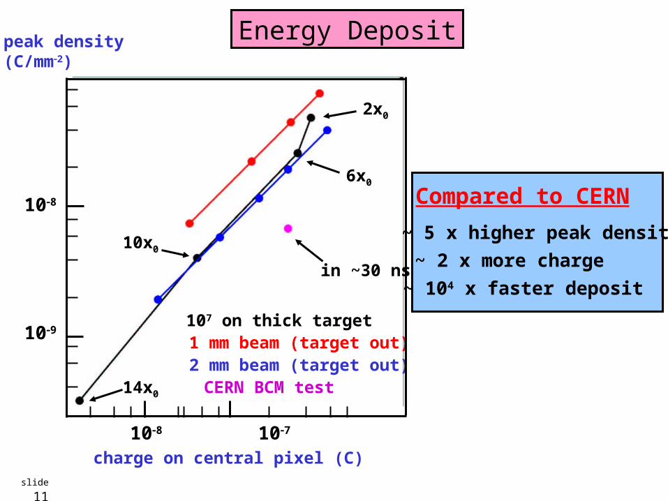
slide 11
Energy Deposit
charge on central pixel (C)
peak density (C/mm2)
107 on thick target1 mm beam (target out)2 mm beam (target out)CERN BCM test
in ~30 ns
14x0
10x0
6x0
2x0
Compared to CERN
~ 5 x higher peak density
~ 2 x more charge
~ 104 x faster deposit
108 107
108
109
slide 12
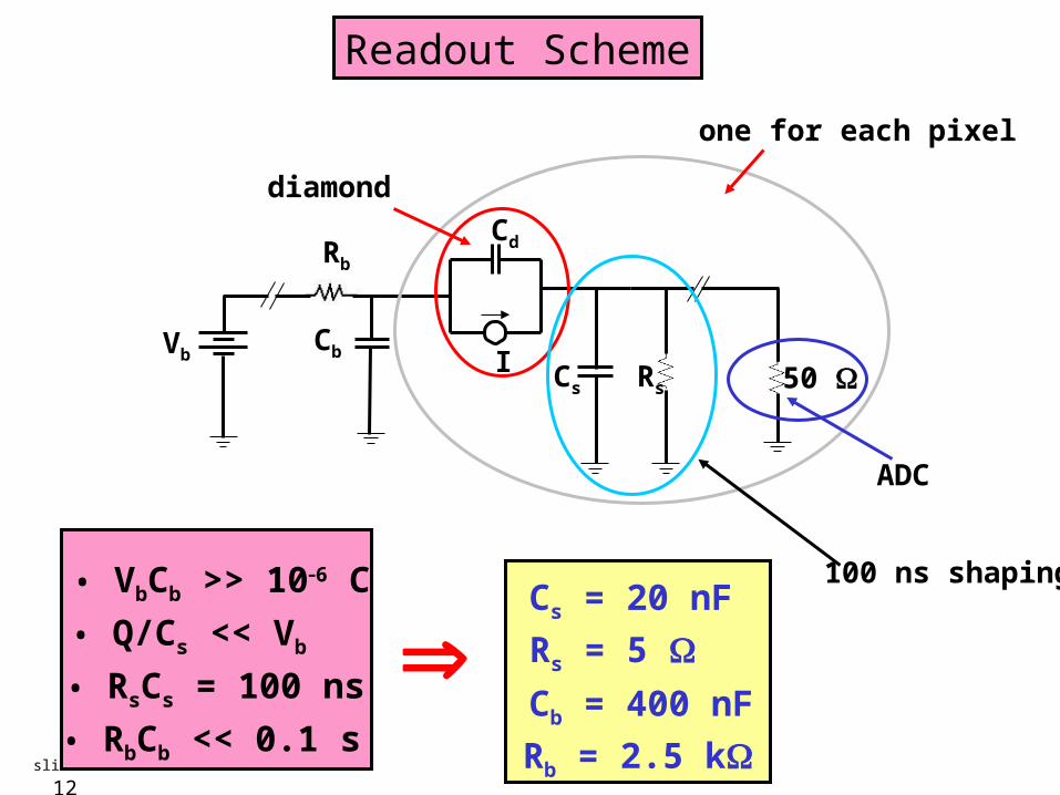
Readout Scheme
Vb
Rb
Cb
Cd
I 50 Cs Rs
diamond
ADC
one for each pixel
• VbCb >> 106 C
• Q/Cs << Vb
• RsCs = 100 ns
• RbCb << 0.1 s
Cs = 20 nF
Rs = 5 Cb = 400 nF
Rb = 2.5 k
100 ns shaping

slide 13
Inductive Voltage Drop
2 x 10⁷ C charge deposited
charge in diamond is collected in about 10 ns
20 A over 10 ns
PC board has to be designed to minimize inductance
this current wants to turn on in ~ 1psthe bunch length of the beam
large inductive voltage drop voltage on diamond sags

slide 14
Inductance
Vb
Rb
Cb
Cd
I CsRs
diamond
inductance a problem here
• wire bond wire and PCB trace about 1 nH per mm
• use multiple wire bonds and traces
• should be able to keep inductance less than 5 nH
causes voltage across diamond to sag
slide 15
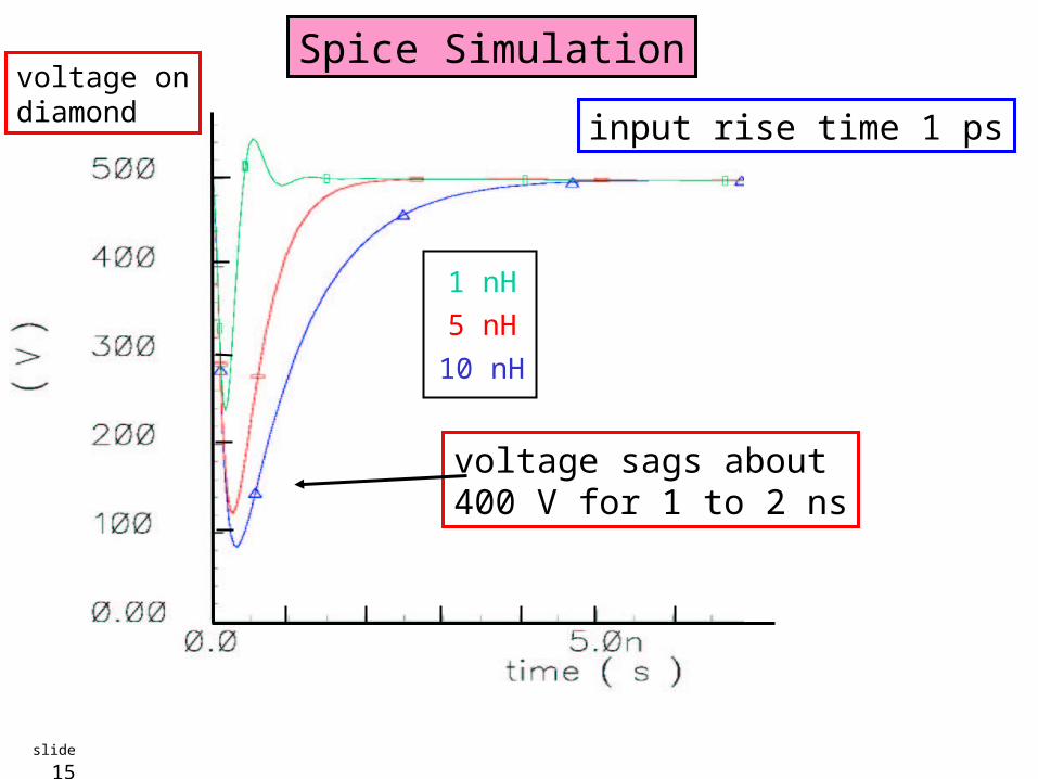
Spice Simulation
10 nH
5 nH
1 nH
voltage sags about400 V for 1 to 2 ns
input rise time 1 ps
voltage ondiamond

slide 16
PC Board
caps as close to diamond as possible
bias linecan have 1 cm hole here
signals routed by flat cable to ganging board
Vb
Rb
Cb
Cd
I CsRs
on ganging board
Cb on backside
on board

slide 17
X/Y Stage
~ 40 cm arm to keep stagesout from behind optical box backscattering
29.5 cm

slide 18
Readout
Diamond PC Board
biascoax
flat signal cable
Ganging Board
from control room
• • •coax signal lines
to control room
one for each diamond
• shaping resistors• ganging of signals
a few feet

slide 19
Issues
• absolute calibration of energy deposit calibrate with direct electron beam
• effect of ionization density vary density and intensity of electron beam
• low energy and stopping electrons need precise GEANT calculation
• neutron background
• current build up
• inductive effects minimize inductance 5 nH 400 V sag over 1 ns
• radiation damage on average 2 x 10¹³ e cm2 hr1 in central pixel we’ll measure it

slide 20
Challenges
• 2 times more charge per pulse than anything previous
• 5 times greater ionization density than anything previous
• First attempt at a few % measurement (10% is the standard)
• Very rapid 1 ps energy deposit