SLAS650E –JUNE 2010–REVISED DECEMBER 2015 ...€“ Fully Integrated LDO With Programmable...
121
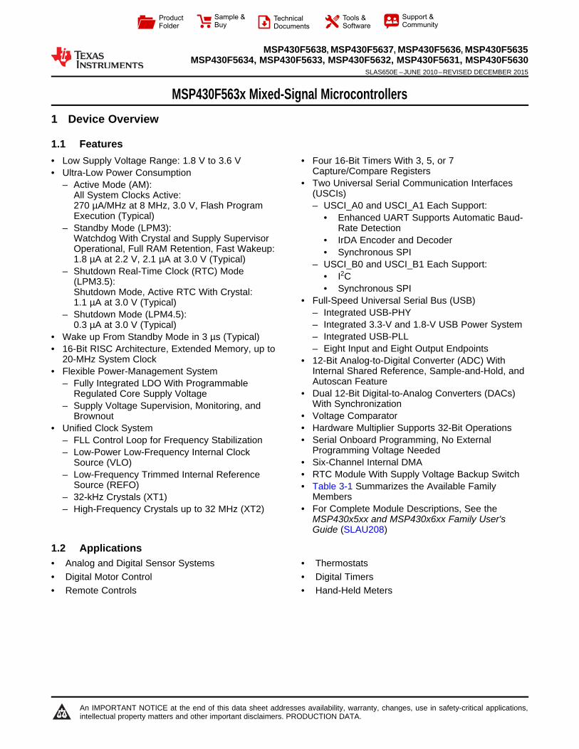
Product Folder Sample & Buy Technical Documents Tools & Software Support & Community MSP430F5638, MSP430F5637, MSP430F5636, MSP430F5635 MSP430F5634, MSP430F5633, MSP430F5632, MSP430F5631, MSP430F5630 SLAS650E – JUNE 2010 – REVISED DECEMBER 2015 MSP430F563x Mixed-Signal Microcontrollers 1 Device Overview 1.1 Features 1 • Low Supply Voltage Range: 1.8 V to 3.6 V • Four 16-Bit Timers With 3, 5, or 7 Capture/Compare Registers • Ultra-Low Power Consumption • Two Universal Serial Communication Interfaces – Active Mode (AM): (USCIs) All System Clocks Active: 270 μA/MHz at 8 MHz, 3.0 V, Flash Program – USCI_A0 and USCI_A1 Each Support: Execution (Typical) • Enhanced UART Supports Automatic Baud- – Standby Mode (LPM3): Rate Detection Watchdog With Crystal and Supply Supervisor • IrDA Encoder and Decoder Operational, Full RAM Retention, Fast Wakeup: • Synchronous SPI 1.8 μA at 2.2 V, 2.1 μA at 3.0 V (Typical) – USCI_B0 and USCI_B1 Each Support: – Shutdown Real-Time Clock (RTC) Mode • I 2 C (LPM3.5): • Synchronous SPI Shutdown Mode, Active RTC With Crystal: • Full-Speed Universal Serial Bus (USB) 1.1 μA at 3.0 V (Typical) – Integrated USB-PHY – Shutdown Mode (LPM4.5): – Integrated 3.3-V and 1.8-V USB Power System 0.3 μA at 3.0 V (Typical) – Integrated USB-PLL • Wake up From Standby Mode in 3 μs (Typical) – Eight Input and Eight Output Endpoints • 16-Bit RISC Architecture, Extended Memory, up to 20-MHz System Clock • 12-Bit Analog-to-Digital Converter (ADC) With Internal Shared Reference, Sample-and-Hold, and • Flexible Power-Management System Autoscan Feature – Fully Integrated LDO With Programmable • Dual 12-Bit Digital-to-Analog Converters (DACs) Regulated Core Supply Voltage With Synchronization – Supply Voltage Supervision, Monitoring, and • Voltage Comparator Brownout • Hardware Multiplier Supports 32-Bit Operations • Unified Clock System • Serial Onboard Programming, No External – FLL Control Loop for Frequency Stabilization Programming Voltage Needed – Low-Power Low-Frequency Internal Clock • Six-Channel Internal DMA Source (VLO) • RTC Module With Supply Voltage Backup Switch – Low-Frequency Trimmed Internal Reference Source (REFO) • Table 3-1 Summarizes the Available Family Members – 32-kHz Crystals (XT1) • For Complete Module Descriptions, See the – High-Frequency Crystals up to 32 MHz (XT2) MSP430x5xx and MSP430x6xx Family User's Guide (SLAU208) 1.2 Applications • Analog and Digital Sensor Systems • Thermostats • Digital Motor Control • Digital Timers • Remote Controls • Hand-Held Meters 1 An IMPORTANT NOTICE at the end of this data sheet addresses availability, warranty, changes, use in safety-critical applications, intellectual property matters and other important disclaimers. PRODUCTION DATA.
-
Upload
duongkhuong -
Category
Documents
-
view
214 -
download
0
Transcript of SLAS650E –JUNE 2010–REVISED DECEMBER 2015 ...€“ Fully Integrated LDO With Programmable...
Product
Folder
Sample &Buy
Technical
Documents
Tools &
Software
Support &Community
MSP430F5638, MSP430F5637, MSP430F5636, MSP430F5635MSP430F5634, MSP430F5633, MSP430F5632, MSP430F5631, MSP430F5630
SLAS650E –JUNE 2010–REVISED DECEMBER 2015
MSP430F563x Mixed-Signal Microcontrollers1 Device Overview
1.1 Features1
• Low Supply Voltage Range: 1.8 V to 3.6 V • Four 16-Bit Timers With 3, 5, or 7Capture/Compare Registers• Ultra-Low Power Consumption
• Two Universal Serial Communication Interfaces– Active Mode (AM):(USCIs)All System Clocks Active:
270 µA/MHz at 8 MHz, 3.0 V, Flash Program – USCI_A0 and USCI_A1 Each Support:Execution (Typical) • Enhanced UART Supports Automatic Baud-
– Standby Mode (LPM3): Rate DetectionWatchdog With Crystal and Supply Supervisor • IrDA Encoder and DecoderOperational, Full RAM Retention, Fast Wakeup: • Synchronous SPI1.8 µA at 2.2 V, 2.1 µA at 3.0 V (Typical) – USCI_B0 and USCI_B1 Each Support:
– Shutdown Real-Time Clock (RTC) Mode • I2C(LPM3.5):• Synchronous SPIShutdown Mode, Active RTC With Crystal:
• Full-Speed Universal Serial Bus (USB)1.1 µA at 3.0 V (Typical)– Integrated USB-PHY– Shutdown Mode (LPM4.5):– Integrated 3.3-V and 1.8-V USB Power System0.3 µA at 3.0 V (Typical)– Integrated USB-PLL• Wake up From Standby Mode in 3 µs (Typical)– Eight Input and Eight Output Endpoints• 16-Bit RISC Architecture, Extended Memory, up to
20-MHz System Clock • 12-Bit Analog-to-Digital Converter (ADC) WithInternal Shared Reference, Sample-and-Hold, and• Flexible Power-Management SystemAutoscan Feature– Fully Integrated LDO With Programmable
• Dual 12-Bit Digital-to-Analog Converters (DACs)Regulated Core Supply VoltageWith Synchronization– Supply Voltage Supervision, Monitoring, and
• Voltage ComparatorBrownout• Hardware Multiplier Supports 32-Bit Operations• Unified Clock System• Serial Onboard Programming, No External– FLL Control Loop for Frequency Stabilization
Programming Voltage Needed– Low-Power Low-Frequency Internal Clock• Six-Channel Internal DMASource (VLO)• RTC Module With Supply Voltage Backup Switch– Low-Frequency Trimmed Internal Reference
Source (REFO) • Table 3-1 Summarizes the Available FamilyMembers– 32-kHz Crystals (XT1)
• For Complete Module Descriptions, See the– High-Frequency Crystals up to 32 MHz (XT2)MSP430x5xx and MSP430x6xx Family User'sGuide (SLAU208)
1.2 Applications• Analog and Digital Sensor Systems • Thermostats• Digital Motor Control • Digital Timers• Remote Controls • Hand-Held Meters
1
An IMPORTANT NOTICE at the end of this data sheet addresses availability, warranty, changes, use in safety-critical applications,intellectual property matters and other important disclaimers. PRODUCTION DATA.

MSP430F5638, MSP430F5637, MSP430F5636, MSP430F5635MSP430F5634, MSP430F5633, MSP430F5632, MSP430F5631, MSP430F5630SLAS650E –JUNE 2010–REVISED DECEMBER 2015 www.ti.com
1.3 DescriptionThe TI MSP430™ family of ultra-low-power microcontrollers consists of several devices featuring differentsets of peripherals targeted for various applications. The architecture, combined with five low-powermodes, is optimized to achieve extended battery life in portable measurement applications. The devicefeatures a powerful 16-bit RISC CPU, 16-bit registers, and constant generators that contribute tomaximum code efficiency. The digitally controlled oscillator (DCO) allows the device to wake up from low-power modes to active mode in 3 µs (typical).
The MSP430F563x devices are microcontrollers with a high-performance 12-bit ADC, a comparator, twoUSCIs, USB 2.0, a hardware multiplier, DMA, four 16-bit timers, an RTC module with alarm capabilities,and up to 74 I/O pins.
Device Information (1)
PART NUMBER PACKAGE BODY SIZE (2)
MSP430F5638IPZ LQFP (100) 14 mm × 14 mmMSP430F5638IZQW BGA (113) 7 mm × 7 mm
(1) For the most current device, package, and ordering information, see the Package Option Addendum inSection 8, or see the TI website at www.ti.com.
(2) The sizes shown here are approximations. For the package dimensions with tolerances, see theMechanical Data in Section 8.
2 Device Overview Copyright © 2010–2015, Texas Instruments IncorporatedSubmit Documentation Feedback
Product Folder Links: MSP430F5638 MSP430F5637 MSP430F5636 MSP430F5635 MSP430F5634 MSP430F5633MSP430F5632 MSP430F5631 MSP430F5630
UnifiedClock
System
256KB192KB128KB
Flash
16KBRAM
+2KB RAMUSB Buffer
+8B BackupRAM
MCLK
ACLK
SMCLK
I/O PortsP1/P2
2×8 I/OsInterrupt
Capability
PA1×16 I/Os
CPUXV2and
WorkingRegisters
EEM(L: 8+2)
XIN XOUT
JTAG/
Interface/
Port PJ
SBW
PA PB PC PD
DMA
6 Channel
XT2IN
XT OUT2
PowerManagement
LDOSVM/Brownout
SVS
SYS
Watchdog
P2 PortMapping
Controller
I/O PortsP3/P4
2×8 I/OsInterrupt
Capability
PB1×16 I/Os
I/O PortsP5/P6
2×8 I/Os
PC1×16 I/Os
I/O PortsP7/P8
1×6 I/Os
PD1×14 I/Os
1×8 I/Os
I/O PortsP9
1×8 I/Os
PE1×8 I/Os
MPY32
TA0
Timer_A5 CC
Registers
TA1 andTA2
2 Timer_Aeach with
3 CCRegisters
TB0
Timer_B7 CC
Registers
CRC16
USCI0,1
Ax: UART,IrDA, SPI
Bx: SPI, I2C
ADC12_A
200 KSPS
16 Channels(12 ext/4 int)
Autoscan
12 Bit
DVCC DVSS AVCC AVSS
P1.x P2.x P3.x P4.x P5.x P6.x P7.x P8.x P9.xRST/NMI
REF
Reference1.5V, 2.0V,
2.5V
USB
Full-speed
Comp_B
PJ.x
RTC_B
BatteryBackupSystem
UnifiedClock
System
256KB192KB128KB
FlashMCLK
ACLK
SMCLK
I/O PortsP1/P2
2×8 I/OsInterrupt
Capability
PA1×16 I/Os
CPUXV2and
WorkingRegisters
EEM(L: 8+2)
XIN XOUT
JTAG/
Interface/
Port PJ
SBW
PA PB PC PD
DMA
6 Channel
XT2IN
XT OUT2
PowerManagement
LDOSVM/Brownout
SVS
SYS
Watchdog
P2 PortMapping
Controller
I/O PortsP3/P4
2×8 I/OsInterrupt
Capability
PB1×16 I/Os
I/O PortsP5/P6
2×8 I/Os
PC1×16 I/Os
I/O PortsP7/P8
1×6 I/Os
PD1×14 I/Os
1×8 I/Os
I/O PortsP9
1×8 I/Os
PE1×8 I/Os
MPY32
TA0
Timer_A5 CC
Registers
TA1 andTA2
2 Timer_Aeach with
3 CCRegisters
TB0
Timer_B7 CC
Registers
RTC_B
BatteryBackupSystem
CRC16
USCI0,1
Ax: UART,IrDA, SPI
Bx: SPI, I2C
ADC12_A
200 KSPS
16 Channels(12 ext/4 int)
Autoscan
12 Bit
DVCC DVSS AVCC AVSS
P1.x P2.x P3.x P4.x P5.x P6.x P7.x P8.x P9.xRST/NMI
REF
Reference1.5V, 2.0V,
2.5V
DAC12_A
12 bit2 channelsvoltage out
USB
Full-speed
Comp_B
PJ.x
16KBRAM
+2KB RAMUSB Buffer
+8B BackupRAM
MSP430F5638, MSP430F5637, MSP430F5636, MSP430F5635MSP430F5634, MSP430F5633, MSP430F5632, MSP430F5631, MSP430F5630
www.ti.com SLAS650E –JUNE 2010–REVISED DECEMBER 2015
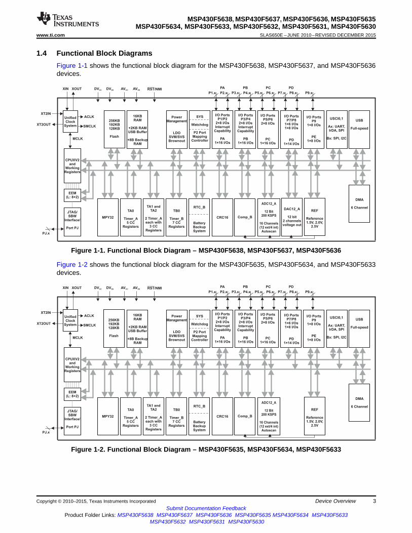
1.4 Functional Block DiagramsFigure 1-1 shows the functional block diagram for the MSP430F5638, MSP430F5637, and MSP430F5636devices.
Figure 1-1. Functional Block Diagram – MSP430F5638, MSP430F5637, MSP430F5636
Figure 1-2 shows the functional block diagram for the MSP430F5635, MSP430F5634, and MSP430F5633devices.
Figure 1-2. Functional Block Diagram – MSP430F5635, MSP430F5634, MSP430F5633
Copyright © 2010–2015, Texas Instruments Incorporated Device Overview 3Submit Documentation Feedback
Product Folder Links: MSP430F5638 MSP430F5637 MSP430F5636 MSP430F5635 MSP430F5634 MSP430F5633MSP430F5632 MSP430F5631 MSP430F5630

UnifiedClock
System
256KB192KB128KB
FlashMCLK
ACLK
SMCLK
I/O PortsP1/P2
2×8 I/OsInterrupt
Capability
PA1×16 I/Os
CPUXV2and
WorkingRegisters
EEM(L: 8+2)
XIN XOUT
JTAG/
Interface/
Port PJ
SBW
PA PB PC PD
DMA
6 Channel
XT2IN
XT OUT2
PowerManagement
LDOSVM/Brownout
SVS
SYS
Watchdog
P2 PortMapping
Controller
I/O PortsP3/P4
2×8 I/OsInterrupt
Capability
PB1×16 I/Os
I/O PortsP5/P6
2×8 I/Os
PC1×16 I/Os
I/O PortsP7/P8
1×6 I/Os
PD1×14 I/Os
1×8 I/Os
I/O PortsP9
1×8 I/Os
PE1×8 I/Os
MPY32
TA0
Timer_A5 CC
Registers
TA1 andTA2
2 Timer_Aeach with
3 CCRegisters
TB0
Timer_B7 CC
Registers
CRC16
USCI0,1
Ax: UART,IrDA, SPI
Bx: SPI, I2C
DVCC DVSS AVCC AVSS
P1.x P2.x P3.x P4.x P5.x P6.x P7.x P8.x P9.xRST/NMI
REF
Reference1.5V, 2.0V,
2.5V
USB
Full-speed
Comp_B
PJ.x
RTC_B
BatteryBackupSystem
16KBRAM
+2KB RAMUSB Buffer
+8B BackupRAM
MSP430F5638, MSP430F5637, MSP430F5636, MSP430F5635MSP430F5634, MSP430F5633, MSP430F5632, MSP430F5631, MSP430F5630SLAS650E –JUNE 2010–REVISED DECEMBER 2015 www.ti.com
Figure 1-3 shows the functional block diagram for the MSP430F5632, MSP430F5631, and MSP430F5630devices.
Figure 1-3. Functional Block Diagram – MSP430F5632, MSP430F5631, MSP430F5630
4 Device Overview Copyright © 2010–2015, Texas Instruments IncorporatedSubmit Documentation Feedback
Product Folder Links: MSP430F5638 MSP430F5637 MSP430F5636 MSP430F5635 MSP430F5634 MSP430F5633MSP430F5632 MSP430F5631 MSP430F5630
MSP430F5638, MSP430F5637, MSP430F5636, MSP430F5635MSP430F5634, MSP430F5633, MSP430F5632, MSP430F5631, MSP430F5630
www.ti.com SLAS650E –JUNE 2010–REVISED DECEMBER 2015
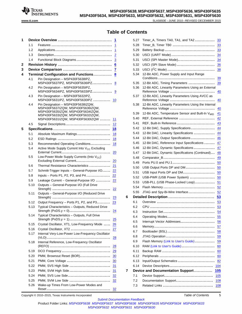
Table of Contents1 Device Overview ......................................... 1 5.27 Timer_A, Timers TA0, TA1, and TA2 ............... 33
1.1 Features .............................................. 1 5.28 Timer_B, Timer TB0 ................................ 331.2 Applications........................................... 1 5.29 Battery Backup ...................................... 331.3 Description............................................ 2 5.30 USCI (UART Mode) ................................. 341.4 Functional Block Diagrams ........................... 3 5.31 USCI (SPI Master Mode)............................ 34
2 Revision History ......................................... 6 5.32 USCI (SPI Slave Mode) ............................. 363 Device Comparison ..................................... 7 5.33 USCI (I2C Mode) .................................... 38
5.34 12-Bit ADC, Power Supply and Input Range4 Terminal Configuration and Functions.............. 8Conditions ........................................... 394.1 Pin Designation – MSP430F5638IPZ,
MSP430F5637IPZ, MSP430F5636IPZ............... 8 5.35 12-Bit ADC, Timing Parameters .................... 394.2 Pin Designation – MSP430F5635IPZ, 5.36 12-Bit ADC, Linearity Parameters Using an External
MSP430F5634IPZ, MSP430F5633IPZ............... 9 Reference Voltage .................................. 404.3 Pin Designation – MSP430F5632IPZ, 5.37 12-Bit ADC, Linearity Parameters Using AVCC as
MSP430F5631IPZ, MSP430F5630IPZ ............. 10 Reference Voltage .................................. 404.4 Pin Designation – MSP430F5638IZQW, 5.38 12-Bit ADC, Linearity Parameters Using the Internal
MSP430F5637IZQW, MSP430F5636IZQW, Reference Voltage .................................. 40MSP430F5635IZQW, MSP430F5634IZQW, 5.39 12-Bit ADC, Temperature Sensor and Built-In VMID 41MSP430F5633IZQW, MSP430F5632IZQW,
5.40 REF, External Reference ........................... 42MSP430F5631IZQW, MSP430F5630IZQW ........ 115.41 REF, Built-In Reference............................. 434.5 Signal Descriptions.................................. 125.42 12-Bit DAC, Supply Specifications .................. 445 Specifications ........................................... 185.43 12-Bit DAC, Linearity Specifications ................ 445.1 Absolute Maximum Ratings ......................... 185.44 12-Bit DAC, Output Specifications .................. 465.2 ESD Ratings ........................................ 185.45 12-Bit DAC, Reference Input Specifications ........ 475.3 Recommended Operating Conditions............... 185.46 12-Bit DAC, Dynamic Specifications ................ 475.4 Active Mode Supply Current Into VCC Excluding
External Current..................................... 20 5.47 12-Bit DAC, Dynamic Specifications (Continued)... 485.5 Low-Power Mode Supply Currents (Into VCC) 5.48 Comparator_B....................................... 49
Excluding External Current.......................... 20 5.49 Ports PU.0 and PU.1................................ 505.6 Thermal Resistance Characteristics ................ 21 5.50 USB Output Ports DP and DM...................... 505.7 Schmitt-Trigger Inputs – General-Purpose I/O...... 22 5.51 USB Input Ports DP and DM........................ 505.8 Inputs – Ports P1, P2, P3, and P4 .................. 22 5.52 USB-PWR (USB Power System) ................... 505.9 Leakage Current – General-Purpose I/O ........... 22 5.53 USB-PLL (USB Phase-Locked Loop) ............... 515.10 Outputs – General-Purpose I/O (Full Drive
5.54 Flash Memory ....................................... 52Strength) ............................................ 225.55 JTAG and Spy-Bi-Wire Interface.................... 525.11 Outputs – General-Purpose I/O (Reduced Drive
6 Detailed Description ................................... 53Strength) ............................................ 236.1 Overview ............................................ 535.12 Output Frequency – Ports P1, P2, and P3.......... 23
5.13 Typical Characteristics – Outputs, Reduced Drive 6.2 CPU ................................................. 53Strength (PxDS.y = 0)............................... 24 6.3 Instruction Set....................................... 54
5.14 Typical Characteristics – Outputs, Full Drive 6.4 Operating Modes.................................... 55Strength (PxDS.y = 1)............................... 25
6.5 Interrupt Vector Addresses.......................... 565.15 Crystal Oscillator, XT1, Low-Frequency Mode ..... 26
6.6 Memory.............................................. 575.16 Crystal Oscillator, XT2 .............................. 27
6.7 Bootloader (BSL) .................................... 585.17 Internal Very-Low-Power Low-Frequency Oscillator
6.8 JTAG Operation ..................................... 59(VLO) ................................................ 286.9 Flash Memory (Link to User's Guide) ............... 595.18 Internal Reference, Low-Frequency Oscillator
(REFO) .............................................. 28 6.10 RAM (Link to User's Guide) ......................... 605.19 DCO Frequency..................................... 29 6.11 Backup RAM ........................................ 605.20 PMM, Brownout Reset (BOR)....................... 30 6.12 Peripherals .......................................... 605.21 PMM, Core Voltage ................................. 30 6.13 Input/Output Schematics ............................ 825.22 PMM, SVS High Side ............................... 31 6.14 Device Descriptors................................. 1045.23 PMM, SVM High Side ............................... 31 7 Device and Documentation Support .............. 1055.24 PMM, SVS Low Side................................ 32 7.1 Device Support..................................... 1055.25 PMM, SVM Low Side ............................... 32 7.2 Documentation Support............................ 1085.26 Wake-up Times From Low-Power Modes and 7.3 Related Links ...................................... 108
Reset ................................................ 32
Copyright © 2010–2015, Texas Instruments Incorporated Table of Contents 5Submit Documentation Feedback
Product Folder Links: MSP430F5638 MSP430F5637 MSP430F5636 MSP430F5635 MSP430F5634 MSP430F5633MSP430F5632 MSP430F5631 MSP430F5630

MSP430F5638, MSP430F5637, MSP430F5636, MSP430F5635MSP430F5634, MSP430F5633, MSP430F5632, MSP430F5631, MSP430F5630SLAS650E –JUNE 2010–REVISED DECEMBER 2015 www.ti.com
7.4 Community Resources............................. 109 7.7 Export Control Notice .............................. 1097.5 Trademarks ........................................ 109 7.8 Glossary............................................ 1097.6 Electrostatic Discharge Caution ................... 109 8 Mechanical, Packaging, and Orderable
Information ............................................. 109
2 Revision HistoryNOTE: Page numbers for previous revisions may differ from page numbers in the current version.
Changes from August 5, 2013 to December 8, 2015 Page
• Document format and organization changes throughout, including addition of section numbering........................ 1• Moved all functional block diagrams to Section 1.4, Functional Block Diagrams ............................................ 3• Added USB column to Table 3-1, Family Members ............................................................................. 7• Added Section 3, Device Comparison, and moved Table 3-1, Family Members to it ....................................... 7• Added "Port U is supplied by the LDOO rail" to the PU.0 and PU.1 descriptions in Table 4-1, Signal Descriptions .. 15• Moved all electrical specifications to Section 5 ................................................................................. 18• Added Section 5.2, ESD Ratings.................................................................................................. 18• Added note to CVCORE............................................................................................................... 18• Added note to RPull .................................................................................................................. 22• Changed TYP value of CL,eff with Test Conditions of "XTS = 0, XCAPx = 0" from 2 pF to 1 pF ......................... 26• In VBAT3 parameter description, changed from "VBAT3 ≠ VBAT/3" to "VBAT3 = VBAT/3" ........................................ 33• Changed from fDAC12_0OUT to fDAC12_1OUT in the first row of the Test Conditions for the "Channel-to-channel
crosstalk" parameter ................................................................................................................ 48• Changed the value of DAC12_xDAT from 7F7h to F7Fh and changed the x-axis label from fToggle to 1/fToggle in
Figure 5-22, Crosstalk Test Conditions .......................................................................................... 48• Added note to RPUR ................................................................................................................. 50• Corrected the spelling of the MRG bits in the fMCLK,MRG parameter ........................................................... 52• Removed RTC_B from LPM4.5 wake-up options............................................................................... 55• Throughout document, changed all instances of "bootstrap loader" to "bootloader" ....................................... 58• Added the paragraph that starts "The application report Using the MSP430 RTC_B..." .................................. 62• Corrected names of interrupt events PMMSWBOR (BOR) and PMMSWPOR (POR) in Table 6-11, System
Module Interrupt Vector Registers ................................................................................................ 63• Corrected spelling of NMIIFG (added missing "I") in Table 6-11, System Module Interrupt Vector Registers.......... 63• Corrected register names (added "USB" prefix as required) in Table 6-50, USB Control Registers..................... 81• Added P7SEL.2 and XT2BYPASS inputs with AND and OR gates in Figure 6-10, Port P7 (P7.3) Schematic ........ 95• Changed P7SEL.3 column from X to 0 for "P7.3 (I/O)" rows.................................................................. 95• Added Section 7 and moved Development Tools Support, Device and Development Tool Nomenclature,
Trademarks, and Electrostatic Discharge Caution sections to it ............................................................ 105• Added Section 8, Mechanical, Packaging, and Orderable Information ..................................................... 109
6 Revision History Copyright © 2010–2015, Texas Instruments IncorporatedSubmit Documentation Feedback
Product Folder Links: MSP430F5638 MSP430F5637 MSP430F5636 MSP430F5635 MSP430F5634 MSP430F5633MSP430F5632 MSP430F5631 MSP430F5630

MSP430F5638, MSP430F5637, MSP430F5636, MSP430F5635MSP430F5634, MSP430F5633, MSP430F5632, MSP430F5631, MSP430F5630
www.ti.com SLAS650E –JUNE 2010–REVISED DECEMBER 2015
3 Device Comparison
Table 3-1 summarizes the available family members.
Table 3-1. Family Members (1) (2)
USCI
CHANNEL CHANNELFLASH SRAM ADC12_A DAC12_A Comp_BDEVICE Timer_A (4) Timer_B (5) USB I/O PACKAGEA: B:(KB) (KB) (3) (Ch) (Ch) (Ch)UART, SPI, I2C
IrDA, SPI
12 ext, 100 PZ,MSP430F5638 256 16 + 2 5, 3, 3 7 2 2 2 12 Yes 744 int 113 ZQW
12 ext, 100 PZ,MSP430F5637 192 16 + 2 5, 3, 3 7 2 2 2 12 Yes 744 int 113 ZQW
12 ext, 100 PZ,MSP430F5636 128 16 + 2 5, 3, 3 7 2 2 2 12 Yes 744 int 113 ZQW
12 ext, 100 PZ,MSP430F5635 256 16 + 2 5, 3, 3 7 2 2 - 12 Yes 744 int 113 ZQW
12 ext, 100 PZ,MSP430F5634 192 16 + 2 5, 3, 3 7 2 2 - 12 Yes 744 int 113 ZQW
12 ext, 100 PZ,MSP430F5633 128 16 + 2 5, 3, 3 7 2 2 - 12 Yes 744 int 113 ZQW
100 PZ,MSP430F5632 256 16 + 2 5, 3, 3 7 2 2 - - 12 Yes 74 113 ZQW
100 PZ,MSP430F5631 192 16 + 2 5, 3, 3 7 2 2 - - 12 Yes 74 113 ZQW
100 PZ,MSP430F5630 128 16 + 2 5, 3, 3 7 2 2 - - 12 Yes 74 113 ZQW
(1) For the most current package and ordering information, see the Package Option Addendum in Section 8, or see the TI website atwww.ti.com.
(2) Package drawings, standard packing quantities, thermal data, symbolization, and PCB design guidelines are available atwww.ti.com/packaging.
(3) The additional 2KB of USB SRAM that is listed can be used as general-purpose SRAM when USB is not in use.(4) Each number in the sequence represents an instantiation of Timer_A with its associated number of capture/compare registers and PWM
output generators available. For example, a number sequence of 3, 5 would represent two instantiations of Timer_A, the firstinstantiation having 3 and the second instantiation having 5 capture/compare registers and PWM output generators, respectively.
(5) Each number in the sequence represents an instantiation of Timer_B with its associated number of capture/compare registers and PWMoutput generators available. For example, a number sequence of 3, 5 would represent two instantiations of Timer_B, the firstinstantiation having 3 and the second instantiation having 5 capture/compare registers and PWM output generators, respectively.
Copyright © 2010–2015, Texas Instruments Incorporated Device Comparison 7Submit Documentation Feedback
Product Folder Links: MSP430F5638 MSP430F5637 MSP430F5636 MSP430F5635 MSP430F5634 MSP430F5633MSP430F5632 MSP430F5631 MSP430F5630

1
2
3
4
5
6
7
8
9
10
11
12
13
14
15
16
17
18
19
20
21
22
23
24
25
76
77
78
79
80
81
82
83
84
85
86
87
88
89
90
91
92
93
94
95
96
97
98
99
100
75
74
73
72
71
70
69
68
67
66
65
64
63
62
61
60
59
58
57
56
55
54
53
52
51
50
49
48
47
46
45
44
43
42
41
40
39
38
37
36
35
34
33
32
31
30
29
28
27
26
P6.4/CB4/A4
P6.5/CB5/A5
P6.6/CB6/A6/DAC0
P6.7/CB7/A7/DAC1
P7.4/CB8/A12
P7.5/CB9/A13
P7.6/CB10/A14/DAC0
P7.7/CB11/A15/DAC1
P5.0/VREF+/VeREF+
P5.1/VREF−/VeREF−
AVCC1
AVSS1
XIN
XOUT
DVCC1
DV
SS
1
VC
OR
E
P5.2
DV
SS
DN
C
P5
.3
P9.7
P9.6
P9.5
P9.4
P9.3
P9.2
P9.1
P9.0
P8.7
P8.6/UCB1SOMI/UCB1SCL
P8.5/UCB1SIMO/UCB1SDA
DVCC2
DVSS2
P2.0/P2MAP0
MSP430F5638MSP430F5637MSP430F5636
PZ PACKAGE(TOP VIEW)
P6.3
/CB
3/A
3
P6.2
/CB
2/A
2
P6.1
/CB
1/A
1
P6.0
/CB
0/A
0
RS
T/N
MI/S
BW
TD
IO
PJ.3
/TC
K
PJ.2
/TM
S
PJ.1
/TD
I/T
CLK
PJ.0
/TD
O
TE
ST
/SB
WT
CK
P7.3
/XT
2O
UT
P7.2
/XT
2IN
VB
US
VU
SB
PU
.1/D
M
PU
R
PU
.0/D
P
VS
SU
V18
AV
SS
3
P1.3
/TA
0.2
P1.4
/TA
0.3
AVSS2
P5.6/ADC12CLK/DMAE0
P5
.4
P5
.5
P1
.0/T
A0
CL
K/A
CL
K
P3
.0/T
A1
CL
K/C
BO
UT
P3
.1/T
A1
.0
P3
.2/T
A1
.1
P1
.6/T
A0
.1
P1
.7/T
A0
.2
P1
.1/T
A0
.0
P1
.2/T
A0
.1
P1
.5/T
A0
.4
P3
.3/T
A1
.2
P3
.4/T
A2
CL
K/S
MC
LK
P3
.5/T
A2
.0
P3
.6/T
A2
.1
P3
.7/T
A2
.2
P4
.0/T
B0
.0
P4.2/TB0.2
P4.1/TB0.1
P4.4/TB0.4
P4.3/TB0.3
P4.6/TB0.6
P4.5/TB0.5
P8.0/TB0CLK
P4.7/TB0OUTH/SVMOUT
P8.4/UCB1CLK/UCA1STE
VB
AK
P2.1/P2MAP1
P2.2/P2MAP2
P2.3/P2MAP3
P2.4/P2MAP4
P2.5/P2MAP5
P2.6/P2MAP6
P2.7/P2MAP7
DV
CC
3
DV
SS
3
VB
AT
P5.7
/RT
CC
LK
P8.1/UCB1STE/UCA1CLK
P8.2/UCA1TXD/UCA1SIMO
P8.3/UCA1RXD/UCA1SOMI
MSP430F5638, MSP430F5637, MSP430F5636, MSP430F5635MSP430F5634, MSP430F5633, MSP430F5632, MSP430F5631, MSP430F5630SLAS650E –JUNE 2010–REVISED DECEMBER 2015 www.ti.com
4 Terminal Configuration and Functions
4.1 Pin Designation – MSP430F5638IPZ, MSP430F5637IPZ, MSP430F5636IPZFigure 4-1 shows the pinout for the MSP430F5638, MSP430F5637, and MSP430F5636 devices in the PZpackage.
NOTE: DNC = Do not connect
Figure 4-1. 100-Pin PZ Package (Top View) – MSP430F5638, MSP430F5637, MSP430F5636
8 Terminal Configuration and Functions Copyright © 2010–2015, Texas Instruments IncorporatedSubmit Documentation Feedback
Product Folder Links: MSP430F5638 MSP430F5637 MSP430F5636 MSP430F5635 MSP430F5634 MSP430F5633MSP430F5632 MSP430F5631 MSP430F5630

1
2
3
4
5
6
7
8
9
10
11
12
13
14
15
16
17
18
19
20
21
22
23
24
25
76
77
78
79
80
81
82
83
84
85
86
87
88
89
90
91
92
93
94
95
96
97
98
99
100
75
74
73
72
71
70
69
68
67
66
65
64
63
62
61
60
59
58
57
56
55
54
53
52
51
50
49
48
47
46
45
44
43
42
41
40
39
38
37
36
35
34
33
32
31
30
29
28
27
26
P6.4/CB4/A4
P6.5/CB5/A5
P6.6/CB6/A6
P6.7/CB7/A7
P7.4/CB8/A12
P7.5/CB9/A13
P7.6/CB10/A14
P7.7/CB11/A15
P5.0/VREF+/VeREF+
P5.1/VREF−/VeREF−
AVCC1
AVSS1
XIN
XOUT
DVCC1
DV
SS
1
VC
OR
E
P5.2
DV
SS
DN
C
P5
.3P9.7
P9.6
P9.5
P9.4
P9.3
P9.2
P9.1
P9.0
P8.7
P8.6/UCB1SOMI/UCB1SCL
P8.5/UCB1SIMO/UCB1SDA
DVCC2
DVSS2
P2.0/P2MAP0
MSP430F5635MSP430F5634MSP430F5633
PZ PACKAGE(TOP VIEW)
P6.3
/CB
3/A
3
P6.2
/CB
2/A
2
P6.1
/CB
1/A
1
P6.0
/CB
0/A
0
RS
T/N
MI/S
BW
TD
IO
PJ.3
/TC
K
PJ.2
/TM
S
PJ.1
/TD
I/T
CLK
PJ.0
/TD
O
TE
ST
/SB
WT
CK
P7.3
/XT
2O
UT
P7.2
/XT
2IN
VB
US
VU
SB
PU
.1/D
M
PU
R
PU
.0/D
P
VS
SU
V18
AV
SS
3
P1.3
/TA
0.2
P1.4
/TA
0.3
AVSS2
P5.6/ADC12CLK/DMAE0
P5
.4
P5
.5
P1
.0/T
A0
CL
K/A
CL
K
P3
.0/T
A1
CL
K/C
BO
UT
P3
.1/T
A1
.0
P3
.2/T
A1
.1
P1
.6/T
A0
.1
P1
.7/T
A0
.2
P1
.1/T
A0
.0
P1
.2/T
A0
.1
P1
.5/T
A0
.4
P3
.3/T
A1
.2
P3
.4/T
A2
CL
K/S
MC
LK
P3
.5/T
A2
.0
P3
.6/T
A2
.1
P3
.7/T
A2
.2
P4
.0/T
B0
.0
P4.2/TB0.2
P4.1/TB0.1
P4.4/TB0.4
P4.3/TB0.3
P4.6/TB0.6
P4.5/TB0.5
P8.0/TB0CLK
P4.7/TB0OUTH/SVMOUT
P8.4/UCB1CLK/UCA1STE
VB
AK
P2.1/P2MAP1
P2.2/P2MAP2
P2.3/P2MAP3
P2.4/P2MAP4
P2.5/P2MAP5
P2.6/P2MAP6
P2.7/P2MAP7
DV
CC
3
DV
SS
3
VB
AT
P5.7
/RT
CC
LK
P8.1/UCB1STE/UCA1CLK
P8.2/UCA1TXD/UCA1SIMO
P8.3/UCA1RXD/UCA1SOMI
MSP430F5638, MSP430F5637, MSP430F5636, MSP430F5635MSP430F5634, MSP430F5633, MSP430F5632, MSP430F5631, MSP430F5630
www.ti.com SLAS650E –JUNE 2010–REVISED DECEMBER 2015
4.2 Pin Designation – MSP430F5635IPZ, MSP430F5634IPZ, MSP430F5633IPZFigure 4-2 shows the pinout for the MSP430F5635, MSP430F5634, and MSP430F5633 devices in the PZpackage.
NOTE: DNC = Do not connect
Figure 4-2. 100-Pin PZ Package (Top View) – MSP430F5635, MSP430F5634, MSP430F5633
Copyright © 2010–2015, Texas Instruments Incorporated Terminal Configuration and Functions 9Submit Documentation Feedback
Product Folder Links: MSP430F5638 MSP430F5637 MSP430F5636 MSP430F5635 MSP430F5634 MSP430F5633MSP430F5632 MSP430F5631 MSP430F5630

1
2
3
4
5
6
7
8
9
10
11
12
13
14
15
16
17
18
19
20
21
22
23
24
25
76
77
78
79
80
81
82
83
84
85
86
87
88
89
90
91
92
93
94
95
96
97
98
99
100
75
74
73
72
71
70
69
68
67
66
65
64
63
62
61
60
59
58
57
56
55
54
53
52
51
50
49
48
47
46
45
44
43
42
41
40
39
38
37
36
35
34
33
32
31
30
29
28
27
26
P6.4/CB4
P6.5/CB5
P6.6/CB6
P6.7/CB7
P7.4/CB8
P7.5/CB9
P7.6/CB10
P7.7/CB11
P5.0/VREF+/VeREF+
P5.1/VREF−/VeREF−
AVCC1
AVSS1
XIN
XOUT
DVCC1
DV
SS
1
VC
OR
E
P5.2
DV
SS
DN
C
P5
.3
P9.7
P9.6
P9.5
P9.4
P9.3
P9.2
P9.1
P9.0
P8.7
P8.6/UCB1SOMI/UCB1SCL
P8.5/UCB1SIMO/UCB1SDA
DVCC2
DVSS2
P2.0/P2MAP0
MSP430F5632MSP430F5631MSP430F5630
PZ PACKAGE(TOP VIEW)
P6.3
/CB
3
P6.2
/CB
2
P6
.1/C
B1
P6.0
/CB
0
RS
T/N
MI/S
BW
TD
IO
PJ.3
/TC
K
PJ.2
/TM
S
PJ.1
/TD
I/T
CLK
PJ.0
/TD
O
TE
ST
/SB
WT
CK
P7.3
/XT
2O
UT
P7.2
/XT
2IN
VB
US
VU
SB
PU
.1/D
M
PU
R
PU
.0/D
P
VS
SU
V18
AV
SS
3
P1.3
/TA
0.2
P1.4
/TA
0.3
AVSS2
P5.6/DMAE0
P5
.4
P5
.5
P1
.0/T
A0
CL
K/A
CL
K
P3
.0/T
A1
CL
K/C
BO
UT
P3
.1/T
A1
.0
P3
.2/T
A1
.1
P1
.6/T
A0
.1
P1
.7/T
A0
.2
P1
.1/T
A0
.0
P1
.2/T
A0
.1
P1
.5/T
A0
.4
P3
.3/T
A1
.2
P3
.4/T
A2
CL
K/S
MC
LK
P3
.5/T
A2
.0
P3
.6/T
A2
.1
P3
.7/T
A2
.2
P4
.0/T
B0
.0
P4.2/TB0.2
P4.1/TB0.1
P4.4/TB0.4
P4.3/TB0.3
P4.6/TB0.6
P4.5/TB0.5
P8.0/TB0CLK
P4.7/TB0OUTH/SVMOUT
P8.4/UCB1CLK/UCA1STE
VB
AK
P2.1/P2MAP1
P2.2/P2MAP2
P2.3/P2MAP3
P2.4/P2MAP4
P2.5/P2MAP5
P2.6/P2MAP6
P2.7/P2MAP7
DV
CC
3
DV
SS
3
VB
AT
P5.7
/RT
CC
LK
P8.1/UCB1STE/UCA1CLK
P8.2/UCA1TXD/UCA1SIMO
P8.3/UCA1RXD/UCA1SOMI
MSP430F5638, MSP430F5637, MSP430F5636, MSP430F5635MSP430F5634, MSP430F5633, MSP430F5632, MSP430F5631, MSP430F5630SLAS650E –JUNE 2010–REVISED DECEMBER 2015 www.ti.com
4.3 Pin Designation – MSP430F5632IPZ, MSP430F5631IPZ, MSP430F5630IPZFigure 4-3 shows the pinout for the MSP430F5632, MSP430F5631, and MSP430F5630 devices in the PZpackage.
NOTE: DNC = Do not connect
Figure 4-3. 100-Pin PZ Package (Top View) – MSP430F5632, MSP430F5631, MSP430F5630
10 Terminal Configuration and Functions Copyright © 2010–2015, Texas Instruments IncorporatedSubmit Documentation Feedback
Product Folder Links: MSP430F5638 MSP430F5637 MSP430F5636 MSP430F5635 MSP430F5634 MSP430F5633MSP430F5632 MSP430F5631 MSP430F5630

A1 A2 A3 A4 A5 A6 A7 A8 A9 A10 A11 A12
B1 B2 B3 B4 B5 B6 B7 B8 B9 B10 B11 B12
C1 C2 C3 C11 C12
D1 D2 D4 D5 D6 D7 D8 D9 D11 D12
E1 E2 E4 E5 E6 E7 E8 E9 E11 E12
F1 F2 F4 F5 F8 F9 F11 F12
G1 G2 G4 G5 G8 G9 G11 G12
J1 J2 J4 J5 J6 J7 J8 J9 J11 J12
H1 H2 H4 H5 H6 H7 H8 H9 H11 H12
K1 K2 K11 K12
L1 L2 L3 L4 L5 L6 L7 L8 L9 L10 L11 L12
M1 M2 M3 M5 M6 M7 M8 M9 M10 M11 M12M4
ZQW PACKAGE(TOP VIEW)
MSP430F5638, MSP430F5637, MSP430F5636, MSP430F5635MSP430F5634, MSP430F5633, MSP430F5632, MSP430F5631, MSP430F5630
www.ti.com SLAS650E –JUNE 2010–REVISED DECEMBER 2015
4.4 Pin Designation – MSP430F5638IZQW, MSP430F5637IZQW, MSP430F5636IZQW,MSP430F5635IZQW, MSP430F5634IZQW, MSP430F5633IZQW, MSP430F5632IZQW,MSP430F5631IZQW, MSP430F5630IZQWFigure 4-4 shows the pin diagram for all devices in the ZQW package. See Section 4.5 for pinassignments and descriptions.
NOTE: For terminal assignments, see Table 4-1
Figure 4-4. 113-Pin ZQW Package (Top View) – MSP430F5638, MSP430F5637, MSP430F5636,MSP430F5635, MSP430F5634, MSP430F5633, MSP430F5632, MSP430F5631, MSP430F5630
Copyright © 2010–2015, Texas Instruments Incorporated Terminal Configuration and Functions 11Submit Documentation Feedback
Product Folder Links: MSP430F5638 MSP430F5637 MSP430F5636 MSP430F5635 MSP430F5634 MSP430F5633MSP430F5632 MSP430F5631 MSP430F5630
MSP430F5638, MSP430F5637, MSP430F5636, MSP430F5635MSP430F5634, MSP430F5633, MSP430F5632, MSP430F5631, MSP430F5630SLAS650E –JUNE 2010–REVISED DECEMBER 2015 www.ti.com
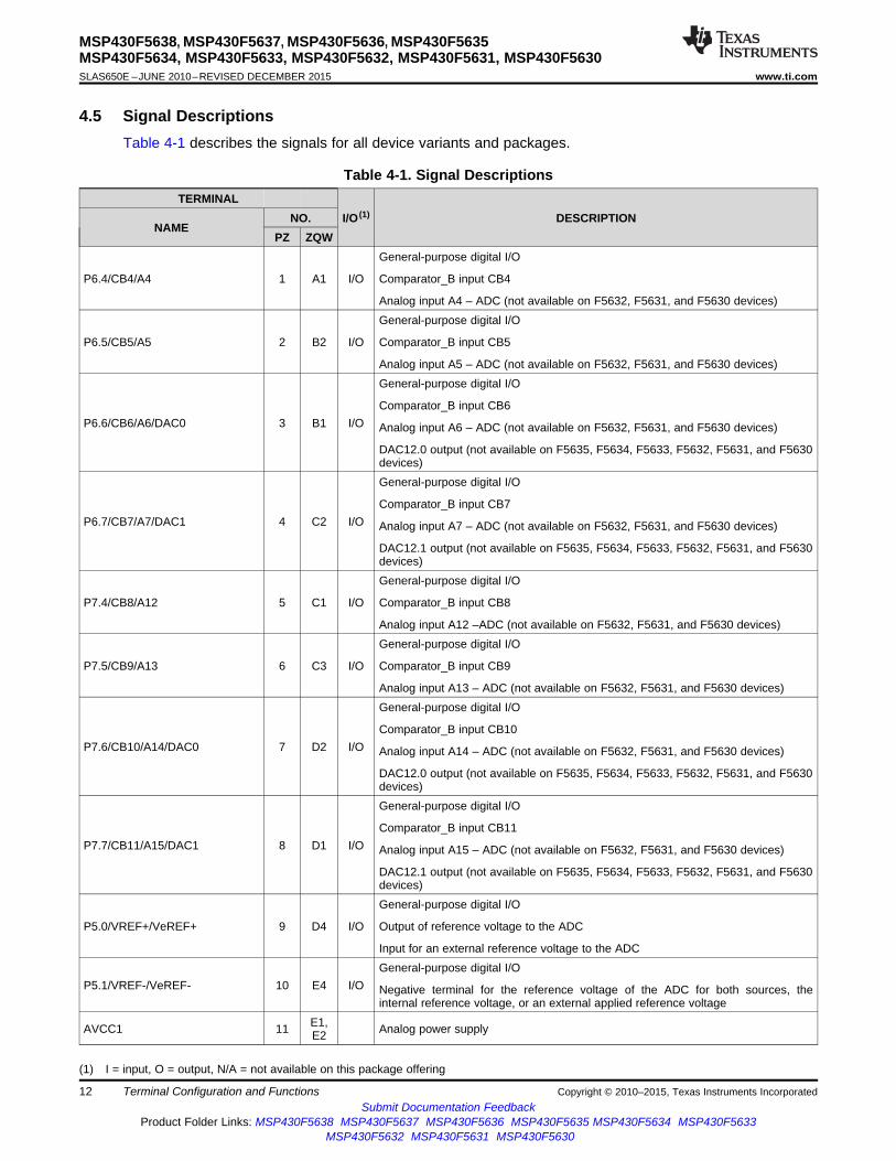
4.5 Signal DescriptionsTable 4-1 describes the signals for all device variants and packages.
Table 4-1. Signal DescriptionsTERMINAL
NO. I/O (1) DESCRIPTIONNAME
PZ ZQWGeneral-purpose digital I/O
P6.4/CB4/A4 1 A1 I/O Comparator_B input CB4
Analog input A4 – ADC (not available on F5632, F5631, and F5630 devices)General-purpose digital I/O
P6.5/CB5/A5 2 B2 I/O Comparator_B input CB5
Analog input A5 – ADC (not available on F5632, F5631, and F5630 devices)General-purpose digital I/O
Comparator_B input CB6P6.6/CB6/A6/DAC0 3 B1 I/O Analog input A6 – ADC (not available on F5632, F5631, and F5630 devices)
DAC12.0 output (not available on F5635, F5634, F5633, F5632, F5631, and F5630devices)General-purpose digital I/O
Comparator_B input CB7P6.7/CB7/A7/DAC1 4 C2 I/O Analog input A7 – ADC (not available on F5632, F5631, and F5630 devices)
DAC12.1 output (not available on F5635, F5634, F5633, F5632, F5631, and F5630devices)General-purpose digital I/O
P7.4/CB8/A12 5 C1 I/O Comparator_B input CB8
Analog input A12 –ADC (not available on F5632, F5631, and F5630 devices)General-purpose digital I/O
P7.5/CB9/A13 6 C3 I/O Comparator_B input CB9
Analog input A13 – ADC (not available on F5632, F5631, and F5630 devices)General-purpose digital I/O
Comparator_B input CB10P7.6/CB10/A14/DAC0 7 D2 I/O Analog input A14 – ADC (not available on F5632, F5631, and F5630 devices)
DAC12.0 output (not available on F5635, F5634, F5633, F5632, F5631, and F5630devices)General-purpose digital I/O
Comparator_B input CB11P7.7/CB11/A15/DAC1 8 D1 I/O Analog input A15 – ADC (not available on F5632, F5631, and F5630 devices)
DAC12.1 output (not available on F5635, F5634, F5633, F5632, F5631, and F5630devices)General-purpose digital I/O
P5.0/VREF+/VeREF+ 9 D4 I/O Output of reference voltage to the ADC
Input for an external reference voltage to the ADCGeneral-purpose digital I/O
P5.1/VREF-/VeREF- 10 E4 I/O Negative terminal for the reference voltage of the ADC for both sources, theinternal reference voltage, or an external applied reference voltage
E1,AVCC1 11 Analog power supplyE2
(1) I = input, O = output, N/A = not available on this package offering
12 Terminal Configuration and Functions Copyright © 2010–2015, Texas Instruments IncorporatedSubmit Documentation Feedback
Product Folder Links: MSP430F5638 MSP430F5637 MSP430F5636 MSP430F5635 MSP430F5634 MSP430F5633MSP430F5632 MSP430F5631 MSP430F5630

MSP430F5638, MSP430F5637, MSP430F5636, MSP430F5635MSP430F5634, MSP430F5633, MSP430F5632, MSP430F5631, MSP430F5630
www.ti.com SLAS650E –JUNE 2010–REVISED DECEMBER 2015
Table 4-1. Signal Descriptions (continued)TERMINAL
NO. I/O (1) DESCRIPTIONNAME
PZ ZQWAVSS1 12 F2 Analog ground supplyXIN 13 F1 I Input terminal for crystal oscillator XT1XOUT 14 G1 O Output terminal of crystal oscillator XT1AVSS2 15 G2 Analog ground supply
General-purpose digital I/O
P5.6/ADC12CLK/DMAE0 16 H1 I/O Conversion clock output ADC (not available on F5632, F5631, and F5630 devices)
DMA external trigger inputGeneral-purpose digital I/O with port interrupt and mappable secondary function
P2.0/P2MAP0 17 G4 I/ODefault mapping: USCI_B0 SPI slave transmit enable; USCI_A0 clock input/outputGeneral-purpose digital I/O with port interrupt and mappable secondary function
P2.1/P2MAP1 18 H2 I/ODefault mapping: USCI_B0 SPI slave in/master out; USCI_B0 I2C dataGeneral-purpose digital I/O with port interrupt and mappable secondary function
P2.2/P2MAP2 19 J1 I/ODefault mapping: USCI_B0 SPI slave out/master in; USCI_B0 I2C clockGeneral-purpose digital I/O with port interrupt and mappable secondary function
P2.3/P2MAP3 20 H4 I/ODefault mapping: USCI_B0 clock input/output; USCI_A0 SPI slave transmit enableGeneral-purpose digital I/O with port interrupt and mappable secondary function
P2.4/P2MAP4 21 J2 I/ODefault mapping: USCI_A0 UART transmit data; USCI_A0 SPI slave in/master outGeneral-purpose digital I/O with port interrupt and mappable secondary function
P2.5/P2MAP5 22 K1 I/ODefault mapping: USCI_A0 UART receive data; USCI_A0 slave out/master inGeneral-purpose digital I/O with port interrupt and mappable secondary function
P2.6/P2MAP6 23 K2 I/ODefault mapping: no secondary functionGeneral-purpose digital I/O with port interrupt and mappable secondary function
P2.7/P2MAP7 24 L2 I/ODefault mapping: no secondary function
DVCC1 25 L1 Digital power supplyDVSS1 26 M1 Digital ground supplyVCORE (2) 27 M2 Regulated core power supply (internal use only, no external current loading)P5.2 28 L3 I/O General-purpose digital I/ODVSS 29 M3 Digital ground supplyDNC 30 J4 Do not connect. It is strongly recommended to leave this terminal open.P5.3 31 L4 I/O General-purpose digital I/OP5.4 32 M4 I/O General-purpose digital I/OP5.5 33 J5 I/O General-purpose digital I/O
General-purpose digital I/O with port interrupt
P1.0/TA0CLK/ACLK 34 L5 I/O Timer TA0 clock signal TACLK input
ACLK output (divided by 1, 2, 4, 8, 16, or 32)General-purpose digital I/O with port interrupt
P1.1/TA0.0 35 M5 I/O Timer TA0 CCR0 capture: CCI0A input, compare: Out0 output
BSL transmit outputGeneral-purpose digital I/O with port interrupt
P1.2/TA0.1 36 J6 I/O Timer TA0 CCR1 capture: CCI1A input, compare: Out1 output
BSL receive input
(2) VCORE is for internal use only. No external current loading is possible. VCORE should only be connected to the recommendedcapacitor value, CVCORE.
Copyright © 2010–2015, Texas Instruments Incorporated Terminal Configuration and Functions 13Submit Documentation Feedback
Product Folder Links: MSP430F5638 MSP430F5637 MSP430F5636 MSP430F5635 MSP430F5634 MSP430F5633MSP430F5632 MSP430F5631 MSP430F5630

MSP430F5638, MSP430F5637, MSP430F5636, MSP430F5635MSP430F5634, MSP430F5633, MSP430F5632, MSP430F5631, MSP430F5630SLAS650E –JUNE 2010–REVISED DECEMBER 2015 www.ti.com
Table 4-1. Signal Descriptions (continued)TERMINAL
NO. I/O (1) DESCRIPTIONNAME
PZ ZQWGeneral-purpose digital I/O with port interrupt
P1.3/TA0.2 37 H6 I/OTimer TA0 CCR2 capture: CCI2A input, compare: Out2 outputGeneral-purpose digital I/O with port interrupt
P1.4/TA0.3 38 M6 I/OTimer TA0 CCR3 capture: CCI3A input compare: Out3 outputGeneral-purpose digital I/O with port interrupt
P1.5/TA0.4 39 L6 I/OTimer TA0 CCR4 capture: CCI4A input, compare: Out4 outputGeneral-purpose digital I/O with port interrupt
P1.6/TA0.1 40 J7 I/OTimer TA0 CCR1 capture: CCI1B input, compare: Out1 outputGeneral-purpose digital I/O with port interrupt
P1.7/TA0.2 41 M7 I/OTimer TA0 CCR2 capture: CCI2B input, compare: Out2 outputGeneral-purpose digital I/O with port interrupt
P3.0/TA1CLK/CBOUT 42 L7 I/O Timer TA1 clock input
Comparator_B outputGeneral-purpose digital I/O with port interrupt
P3.1/TA1.0 43 H7 I/OTimer TA1 capture CCR0: CCI0A/CCI0B input, compare: Out0 outputGeneral-purpose digital I/O with port interrupt
P3.2/TA1.1 44 M8 I/OTimer TA1 capture CCR1: CCI1A/CCI1B input, compare: Out1 outputGeneral-purpose digital I/O with port interrupt
P3.3/TA1.2 45 L8 I/OTimer TA1 capture CCR2: CCI2A/CCI2B input, compare: Out2 outputGeneral-purpose digital I/O with port interrupt
P3.4/TA2CLK/SMCLK 46 J8 I/O Timer TA2 clock input
SMCLK outputGeneral-purpose digital I/O with port interrupt
P3.5/TA2.0 47 M9 I/OTimer TA2 capture CCR0: CCI0A/CCI0B input, compare: Out0 outputGeneral-purpose digital I/O with port interrupt
P3.6/TA2.1 48 L9 I/OTimer TA2 capture CCR1: CCI1A/CCI1B input, compare: Out1 outputGeneral-purpose digital I/O with port interrupt
P3.7/TA2.2 49 M10 I/OTimer TA2 capture CCR2: CCI2A/CCI2B input, compare: Out2 outputGeneral-purpose digital I/O with port interrupt
P4.0/TB0.0 50 J9 I/OTimer TB0 capture CCR0: CCI0A/CCI0B input, compare: Out0 outputGeneral-purpose digital I/O with port interrupt
P4.1/TB0.1 51 M11 I/OTimer TB0 capture CCR1: CCI1A/CCI1B input, compare: Out1 outputGeneral-purpose digital I/O with port interrupt
P4.2/TB0.2 52 L10 I/OTimer TB0 capture CCR2: CCI2A/CCI2B input, compare: Out2 outputGeneral-purpose digital I/O with port interrupt
P4.3/TB0.3 53 M12 I/OTimer TB0 capture CCR3: CCI3A/CCI3B input, compare: Out3 outputGeneral-purpose digital I/O with port interrupt
P4.4/TB0.4 54 L12 I/OTimer TB0 capture CCR4: CCI4A/CCI4B input, compare: Out4 outputGeneral-purpose digital I/O with port interrupt
P4.5/TB0.5 55 L11 I/OTimer TB0 capture CCR5: CCI5A/CCI5B input, compare: Out5 outputGeneral-purpose digital I/O with port interrupt
P4.6/TB0.6 56 K11 I/OTimer TB0 capture CCR6: CCI6A/CCI6B input, compare: Out6 output
14 Terminal Configuration and Functions Copyright © 2010–2015, Texas Instruments IncorporatedSubmit Documentation Feedback
Product Folder Links: MSP430F5638 MSP430F5637 MSP430F5636 MSP430F5635 MSP430F5634 MSP430F5633MSP430F5632 MSP430F5631 MSP430F5630
MSP430F5638, MSP430F5637, MSP430F5636, MSP430F5635MSP430F5634, MSP430F5633, MSP430F5632, MSP430F5631, MSP430F5630
www.ti.com SLAS650E –JUNE 2010–REVISED DECEMBER 2015
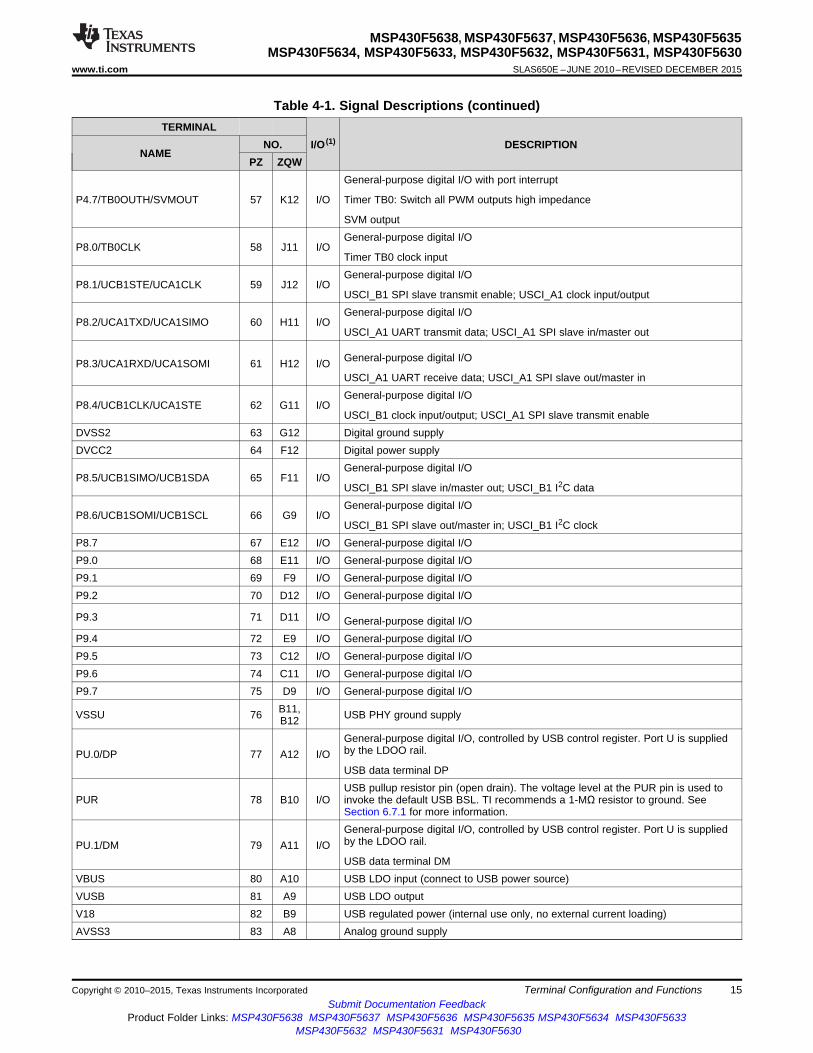
Table 4-1. Signal Descriptions (continued)TERMINAL
NO. I/O (1) DESCRIPTIONNAME
PZ ZQWGeneral-purpose digital I/O with port interrupt
P4.7/TB0OUTH/SVMOUT 57 K12 I/O Timer TB0: Switch all PWM outputs high impedance
SVM outputGeneral-purpose digital I/O
P8.0/TB0CLK 58 J11 I/OTimer TB0 clock inputGeneral-purpose digital I/O
P8.1/UCB1STE/UCA1CLK 59 J12 I/OUSCI_B1 SPI slave transmit enable; USCI_A1 clock input/outputGeneral-purpose digital I/O
P8.2/UCA1TXD/UCA1SIMO 60 H11 I/OUSCI_A1 UART transmit data; USCI_A1 SPI slave in/master out
General-purpose digital I/OP8.3/UCA1RXD/UCA1SOMI 61 H12 I/OUSCI_A1 UART receive data; USCI_A1 SPI slave out/master inGeneral-purpose digital I/O
P8.4/UCB1CLK/UCA1STE 62 G11 I/OUSCI_B1 clock input/output; USCI_A1 SPI slave transmit enable
DVSS2 63 G12 Digital ground supplyDVCC2 64 F12 Digital power supply
General-purpose digital I/OP8.5/UCB1SIMO/UCB1SDA 65 F11 I/O
USCI_B1 SPI slave in/master out; USCI_B1 I2C dataGeneral-purpose digital I/O
P8.6/UCB1SOMI/UCB1SCL 66 G9 I/OUSCI_B1 SPI slave out/master in; USCI_B1 I2C clock
P8.7 67 E12 I/O General-purpose digital I/OP9.0 68 E11 I/O General-purpose digital I/OP9.1 69 F9 I/O General-purpose digital I/OP9.2 70 D12 I/O General-purpose digital I/O
P9.3 71 D11 I/O General-purpose digital I/OP9.4 72 E9 I/O General-purpose digital I/OP9.5 73 C12 I/O General-purpose digital I/OP9.6 74 C11 I/O General-purpose digital I/OP9.7 75 D9 I/O General-purpose digital I/O
B11,VSSU 76 USB PHY ground supplyB12General-purpose digital I/O, controlled by USB control register. Port U is suppliedby the LDOO rail.PU.0/DP 77 A12 I/OUSB data terminal DPUSB pullup resistor pin (open drain). The voltage level at the PUR pin is used to
PUR 78 B10 I/O invoke the default USB BSL. TI recommends a 1-MΩ resistor to ground. SeeSection 6.7.1 for more information.General-purpose digital I/O, controlled by USB control register. Port U is suppliedby the LDOO rail.PU.1/DM 79 A11 I/OUSB data terminal DM
VBUS 80 A10 USB LDO input (connect to USB power source)VUSB 81 A9 USB LDO outputV18 82 B9 USB regulated power (internal use only, no external current loading)AVSS3 83 A8 Analog ground supply
Copyright © 2010–2015, Texas Instruments Incorporated Terminal Configuration and Functions 15Submit Documentation Feedback
Product Folder Links: MSP430F5638 MSP430F5637 MSP430F5636 MSP430F5635 MSP430F5634 MSP430F5633MSP430F5632 MSP430F5631 MSP430F5630

MSP430F5638, MSP430F5637, MSP430F5636, MSP430F5635MSP430F5634, MSP430F5633, MSP430F5632, MSP430F5631, MSP430F5630SLAS650E –JUNE 2010–REVISED DECEMBER 2015 www.ti.com
Table 4-1. Signal Descriptions (continued)TERMINAL
NO. I/O (1) DESCRIPTIONNAME
PZ ZQWGeneral-purpose digital I/O
P7.2/XT2IN 84 B8 I/OInput terminal for crystal oscillator XT2General-purpose digital I/O
P7.3/XT2OUT 85 B7 I/OOutput terminal of crystal oscillator XT2Capacitor for backup subsystem. Do not load this pin externally. For capacitorVBAK 86 A7 values, see CBAK in Recommended Operating Conditions.Backup or secondary supply voltage. If backup voltage is not supplied, connect toVBAT 87 D8 DVCC externally.General-purpose digital I/O
P5.7/RTCCLK 88 D7 I/ORTCCLK output
DVCC3 89 A6 Digital power supplyDVSS3 90 A5 Digital ground supply
Test mode pin; selects digital I/O on JTAG pinsTEST/SBWTCK 91 B6 I
Spy-Bi-Wire input clockGeneral-purpose digital I/O
PJ.0/TDO 92 B5 I/OTest data output portGeneral-purpose digital I/O
PJ.1/TDI/TCLK 93 A4 I/OTest data input or test clock inputGeneral-purpose digital I/O
PJ.2/TMS 94 E7 I/OTest mode selectGeneral-purpose digital I/O
PJ.3/TCK 95 D6 I/OTest clockReset input (active low) (3)
RST/NMI/SBWTDIO 96 A3 I/O Nonmaskable interrupt input
Spy-Bi-Wire data input/outputGeneral-purpose digital I/O
P6.0/CB0/A0 97 B4 I/O Comparator_B input CB0
Analog input A0 – ADC (not available on F5632, F5631, and F5630 devices)General-purpose digital I/O
P6.1/CB1/A1 98 B3 I/O Comparator_B input CB1
Analog input A1 – ADC (not available on F5632, F5631, and F5630 devices)General-purpose digital I/O
P6.2/CB2/A2 99 A2 I/O Comparator_B input CB2
Analog input A2 – ADC (not available on F5632, F5631, and F5630 devices)General-purpose digital I/O
P6.3/CB3/A3 100 D5 I/O Comparator_B input CB3
Analog input A3 – ADC (not available on F5632, F5631, and F5630 devices)
(3) When this pin is configured as reset, the internal pullup resistor is enabled by default.
16 Terminal Configuration and Functions Copyright © 2010–2015, Texas Instruments IncorporatedSubmit Documentation Feedback
Product Folder Links: MSP430F5638 MSP430F5637 MSP430F5636 MSP430F5635 MSP430F5634 MSP430F5633MSP430F5632 MSP430F5631 MSP430F5630

MSP430F5638, MSP430F5637, MSP430F5636, MSP430F5635MSP430F5634, MSP430F5633, MSP430F5632, MSP430F5631, MSP430F5630
www.ti.com SLAS650E –JUNE 2010–REVISED DECEMBER 2015
Table 4-1. Signal Descriptions (continued)TERMINAL
NO. I/O (1) DESCRIPTIONNAME
PZ ZQWE5,E6,E8,F4,F5,
Reserved N/A F8, Reserved. TI recommends connecting to ground (DVSS, AVSS).G5,G8,H5,H8,H9
Copyright © 2010–2015, Texas Instruments Incorporated Terminal Configuration and Functions 17Submit Documentation Feedback
Product Folder Links: MSP430F5638 MSP430F5637 MSP430F5636 MSP430F5635 MSP430F5634 MSP430F5633MSP430F5632 MSP430F5631 MSP430F5630

MSP430F5638, MSP430F5637, MSP430F5636, MSP430F5635MSP430F5634, MSP430F5633, MSP430F5632, MSP430F5631, MSP430F5630SLAS650E –JUNE 2010–REVISED DECEMBER 2015 www.ti.com
5 Specifications
5.1 Absolute Maximum Ratings (1)
over operating free-air temperature range (unless otherwise noted)MIN MAX UNIT
Voltage applied at VCC to VSS –0.3 4.1 VVoltage applied to any pin (excluding VCORE, VBUS, V18) (2) –0.3 VCC + 0.3 VDiode current at any device pin ±2 mAMaximum junction temperature, TJ 95 °CStorage temperature, Tstg
(3) –55 150 °C
(1) Stresses beyond those listed under Absolute Maximum Ratings may cause permanent damage to the device. These are stress ratingsonly, and functional operation of the device at these or any other conditions beyond those indicated under Recommended OperatingConditions is not implied. Exposure to absolute-maximum-rated conditions for extended periods may affect device reliability.
(2) All voltages referenced to VSS. VCORE is for internal device use only. No external DC loading or voltage should be applied.(3) Higher temperature may be applied during board soldering according to the current JEDEC J-STD-020 specification with peak reflow
temperatures not higher than classified on the device label on the shipping boxes or reels.
5.2 ESD RatingsVALUE UNIT
Human-body model (HBM), per ANSI/ESDA/JEDEC JS-001 (1) ±1000V(ESD) Electrostatic discharge V
Charged-device model (CDM), per JEDEC specification JESD22-C101 (2) ±250
(1) JEDEC document JEP155 states that 500-V HBM allows safe manufacturing with a standard ESD control process. Pins listed as±1000 V may actually have higher performance.
(2) JEDEC document JEP157 states that 250-V CDM allows safe manufacturing with a standard ESD control process. Pins listed as ±250 Vmay actually have higher performance.
5.3 Recommended Operating ConditionsMIN NOM MAX UNIT
PMMCOREVx = 0 1.8 3.6Supply voltage during program execution and flash PMMCOREVx = 0, 1 2.0 3.6
VCC programming (AVCC1 = DVCC1 = DVCC2 = DVCC3 = VPMMCOREVx = 0, 1, 2 2.2 3.6DVCC = VCC) (1) (2)
PMMCOREVx = 0, 1, 2, 3 2.4 3.6PMMCOREVx = 0 1.8 3.6PMMCOREVx = 0, 1 2.0 3.6Supply voltage during USB operation, USB PLL disabled
(USB_EN = 1, UPLLEN = 0) PMMCOREVx = 0, 1, 2 2.2 3.6VCC,USB V
PMMCOREVx = 0, 1, 2, 3 2.4 3.6PMMCOREVx = 2 2.2 3.6Supply voltage during USB operation, USB PLL enabled (3)
(USB_EN = 1, UPLLEN = 1) PMMCOREVx = 2, 3 2.4 3.6Supply voltage (AVSS1 = AVSS2 = AVSS3 = DVSS1 =VSS 0 VDVSS2 = DVSS3 = VSS)
TA = 0°C to 85°C 1.55 3.6VBAT,RTC Backup-supply voltage with RTC operational V
TA = –40°C to +85°C 1.70 3.6VBAT,MEM Backup-supply voltage with backup memory retained TA = –40°C to +85°C 1.20 3.6 VTA Operating free-air temperature I version –40 85 °CTJ Operating junction temperature I version –40 85 °CCBAK Capacitance at pin VBAK 1 4.7 10 nFCVCORE Capacitor at VCORE (4) 470 nF
(1) TI recommends powering AVCC and DVCC from the same source. A maximum difference of 0.3 V between AVCC and DVCC can betolerated during power up and operation.
(2) The minimum supply voltage is defined by the supervisor SVS levels when it is enabled. See the threshold parameters in Section 5.22for the exact values and further details.
(3) USB operation with USB PLL enabled requires PMMCOREVx ≥ 2 for proper operation.(4) A capacitor tolerance of ±20% or better is required.
18 Specifications Copyright © 2010–2015, Texas Instruments IncorporatedSubmit Documentation Feedback
Product Folder Links: MSP430F5638 MSP430F5637 MSP430F5636 MSP430F5635 MSP430F5634 MSP430F5633MSP430F5632 MSP430F5631 MSP430F5630

2.01.8
8
0
12
20
25
Syste
m F
requency -
MH
z
Supply Voltage - V
The numbers within the fields denote the supported PMMCOREVx settings.
2.2 2.4 3.6
0, 1, 2, 30, 1, 20, 10
1, 2, 31, 21
2, 3
3
2
16
MSP430F5638, MSP430F5637, MSP430F5636, MSP430F5635MSP430F5634, MSP430F5633, MSP430F5632, MSP430F5631, MSP430F5630
www.ti.com SLAS650E –JUNE 2010–REVISED DECEMBER 2015
Recommended Operating Conditions (continued)MIN NOM MAX UNIT
CDVCC/ Capacitor ratio of DVCC to VCORE 10CVCORE
PMMCOREVx = 0,1.8 V ≤ VCC ≤ 3.6 V 0 8.0(default condition)PMMCOREVx = 1, 0 12.0Processor frequency (maximum MCLK frequency) (5) (6)2 V ≤ VCC ≤ 3.6 VfSYSTEM MHz(see Figure 5-1)PMMCOREVx = 2, 0 16.02.2 V ≤ VCC ≤ 3.6 VPMMCOREVx = 3, 0 20.02.4 V ≤ VCC ≤ 3.6 V
fSYSTEM_USB Minimum processor frequency for USB operation 1.5 MHzUSB_wait Wait state cycles during USB operation 16 cycles
(5) The MSP430 CPU is clocked directly with MCLK. Both the high and low phase of MCLK must not exceed the pulse duration of thespecified maximum frequency.
(6) Modules may have a different maximum input clock specification. See the specification of the respective module in this data sheet.
Figure 5-1. Frequency vs Supply Voltage
Copyright © 2010–2015, Texas Instruments Incorporated Specifications 19Submit Documentation Feedback
Product Folder Links: MSP430F5638 MSP430F5637 MSP430F5636 MSP430F5635 MSP430F5634 MSP430F5633MSP430F5632 MSP430F5631 MSP430F5630

MSP430F5638, MSP430F5637, MSP430F5636, MSP430F5635MSP430F5634, MSP430F5633, MSP430F5632, MSP430F5631, MSP430F5630SLAS650E –JUNE 2010–REVISED DECEMBER 2015 www.ti.com
5.4 Active Mode Supply Current Into VCC Excluding External Currentover recommended operating free-air temperature (unless otherwise noted) (1) (2) (3)
FREQUENCY (fDCO = fMCLK = fSMCLK)EXECUTIONPARAMETER VCC PMMCOREVx 1 MHz 8 MHz 12 MHz 20 MHz UNITMEMORY
TYP MAX TYP MAX TYP MAX TYP MAX0 0.32 0.36 2.1 2.41 0.36 2.4 3.6 4.0
IAM, Flash Flash 3 V mA2 0.37 2.5 3.83 0.39 2.7 4.0 6.60 0.18 0.21 1.0 1.21 0.20 1.2 1.7 1.9
IAM, RAM RAM 3 V mA2 0.22 1.3 2.03 0.23 1.4 2.1 3.6
(1) All inputs are tied to 0 V or to VCC. Outputs do not source or sink any current.(2) The currents are characterized with a Micro Crystal MS1V-T1K crystal with a load capacitance of 12.5 pF. The internal and external load
capacitance are chosen to closely match the required 12.5 pF.(3) Characterized with program executing typical data processing. USB disabled (VUSBEN = 0, SLDOEN = 0).
fACLK = 32786 Hz, fDCO = fMCLK = fSMCLK at specified frequency.XTS = CPUOFF = SCG0 = SCG1 = OSCOFF = SMCLKOFF = 0.
5.5 Low-Power Mode Supply Currents (Into VCC) Excluding External Currentover recommended ranges of supply voltage and operating free-air temperature (unless otherwise noted) (1) (2)
–40°C 25°C 60°C 85°CPARAMETER VCC PMMCOREVx UNIT
TYP MAX TYP MAX TYP MAX TYP MAX2.2 V 0 71 75 87 81 85 99
ILPM0,1MHz Low-power mode 0 (3) (4) µA3 V 3 78 83 98 89 94 108
2.2 V 0 6.3 6.7 9.9 9.0 11 16ILPM2 Low-power mode 2 (5) (4) µA
3 V 3 6.6 7.0 11 10 12 180 1.6 1.8 2.4 4.7 6.5 10.5
2.2 V 1 1.6 1.9 4.8 6.62 1.7 2.0 4.9 6.7
Low-power mode 3,ILPM3,XT1LF 0 1.9 2.1 2.7 5.0 6.8 10.8 µAcrystal mode (6) (4)
1 1.9 2.1 5.1 7.03 V
2 2.0 2.2 5.2 7.13 2.0 2.2 2.9 5.4 7.3 12.6
(1) All inputs are tied to 0 V or to VCC. Outputs do not source or sink any current.(2) The currents are characterized with a Micro Crystal CC4V-T1A SMD crystal with a load capacitance of 9 pF. The internal and external
load capacitance are chosen to closely match the required 9 pF.(3) Current for watchdog timer clocked by SMCLK included. ACLK = low-frequency crystal operation (XTS = 0, XT1DRIVEx = 0).
CPUOFF = 1, SCG0 = 0, SCG1 = 0, OSCOFF = 0 (LPM0), fACLK = 32768 Hz, fMCLK = 0 MHz, fSMCLK = fDCO = 1 MHzUSB disabled (VUSBEN = 0, SLDOEN = 0).
(4) Current for brownout included. Low-side supervisor and monitors disabled (SVSL, SVML). High-side supervisor and monitor disabled(SVSH, SVMH). RAM retention enabled.
(5) Current for watchdog timer clocked by ACLK and RTC clocked by LFXT1 (32768 Hz) included. ACLK = low-frequency crystal operation(XTS = 0, XT1DRIVEx = 0).CPUOFF = 1, SCG0 = 0, SCG1 = 1, OSCOFF = 0 (LPM2), fACLK = 32768 Hz, fMCLK = 0 MHz, fSMCLK = fDCO = 0 MHz; DCOsetting = 1 MHz operation, DCO bias generator enabled.USB disabled (VUSBEN = 0, SLDOEN = 0).
(6) Current for watchdog timer clocked by ACLK and RTC clocked by LFXT1 (32768 Hz) included. ACLK = low-frequency crystal operation(XTS = 0, XT1DRIVEx = 0).CPUOFF = 1, SCG0 = 1, SCG1 = 1, OSCOFF = 0 (LPM3), fACLK = 32768 Hz, fMCLK = fSMCLK = fDCO = 0 MHzUSB disabled (VUSBEN = 0, SLDOEN = 0).
20 Specifications Copyright © 2010–2015, Texas Instruments IncorporatedSubmit Documentation Feedback
Product Folder Links: MSP430F5638 MSP430F5637 MSP430F5636 MSP430F5635 MSP430F5634 MSP430F5633MSP430F5632 MSP430F5631 MSP430F5630
MSP430F5638, MSP430F5637, MSP430F5636, MSP430F5635MSP430F5634, MSP430F5633, MSP430F5632, MSP430F5631, MSP430F5630
www.ti.com SLAS650E –JUNE 2010–REVISED DECEMBER 2015
Low-Power Mode Supply Currents (Into VCC) Excluding External Current (continued)over recommended ranges of supply voltage and operating free-air temperature (unless otherwise noted)(1)(2)
–40°C 25°C 60°C 85°CPARAMETER VCC PMMCOREVx UNIT
TYP MAX TYP MAX TYP MAX TYP MAX0 0.9 1.2 1.9 4.0 5.9 10.3
Low-power mode 3, 1 0.9 1.2 4.1 6.0ILPM3, VLO mode, Watchdog 3 V µAVLO,WDT 2 1.0 1.3 4.2 6.1enabled (7) (4)
3 1.0 1.3 2.2 4.3 6.3 11.30 0.9 1.1 1.8 3.9 5.8 101 0.9 1.1 4.0 5.9
ILPM4 Low-power mode 4 (8) (4) 3 V µA2 1.0 1.2 4.1 6.13 1.0 1.2 2.1 4.2 6.2 11
Low-power mode 3.5ILPM3.5, (LPM3.5) current with 3 V 0.5 0.8 1.4 µARTC,VCC active RTC into primary
supply pin DVCC(9)
Low-power mode 3.5ILPM3.5, (LPM3.5) current with 3 V 0.6 0.8 1.4 µARTC,VBAT active RTC into backup
supply pin VBAT (10)
Total low-power modeILPM3.5, 3.5 (LPM3.5) current 3 V 1.0 1.1 1.3 1.6 2.8 µARTC,TOT with active RTC (11)
Low-power mode 4.5ILPM4.5 3 V 0.2 0.3 0.6 0.7 0.9 1.4 µA(LPM4.5) (12)
(7) Current for watchdog timer clocked by VLO included.CPUOFF = 1, SCG0 = 1, SCG1 = 1, OSCOFF = 0 (LPM3), fACLK = fMCLK = fSMCLK = fDCO = 0 MHzUSB disabled (VUSBEN = 0, SLDOEN = 0).
(8) CPUOFF = 1, SCG0 = 1, SCG1 = 1, OSCOFF = 1 (LPM4), fDCO = fACLK = fMCLK = fSMCLK = 0 MHzUSB disabled (VUSBEN = 0, SLDOEN = 0).
(9) VVBAT = VCC - 0.2 V, fDCO = fMCLK = fSMCLK = 0 MHz, fACLK = 32768 Hz, PMMREGOFF = 1, RTC in backup domain active(10) VVBAT = VCC - 0.2 V, fDCO = fMCLK = fSMCLK = 0 MHz, fACLK = 32768 Hz, PMMREGOFF = 1, RTC in backup domain active, no
current drawn on VBAK(11) fDCO = fMCLK = fSMCLK = 0 MHz, fACLK = 32768 Hz, PMMREGOFF = 1, RTC in backup domain active, no current drawn on VBAK(12) Internal regulator disabled. No data retention.
CPUOFF = 1, SCG0 = 1, SCG1 = 1, OSCOFF = 1, PMMREGOFF = 1 (LPM4.5), fDCO = fACLK = fMCLK = fSMCLK = 0 MHz
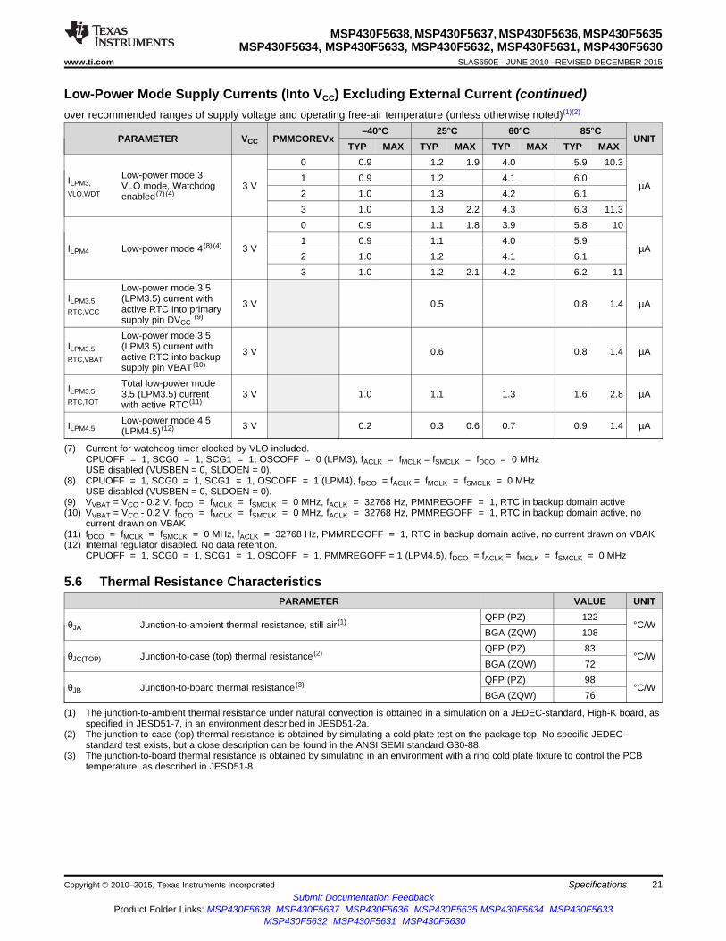
5.6 Thermal Resistance CharacteristicsPARAMETER VALUE UNIT
QFP (PZ) 122θJA Junction-to-ambient thermal resistance, still air (1) °C/W
BGA (ZQW) 108QFP (PZ) 83
θJC(TOP) Junction-to-case (top) thermal resistance (2) °C/WBGA (ZQW) 72QFP (PZ) 98
θJB Junction-to-board thermal resistance (3) °C/WBGA (ZQW) 76
(1) The junction-to-ambient thermal resistance under natural convection is obtained in a simulation on a JEDEC-standard, High-K board, asspecified in JESD51-7, in an environment described in JESD51-2a.
(2) The junction-to-case (top) thermal resistance is obtained by simulating a cold plate test on the package top. No specific JEDEC-standard test exists, but a close description can be found in the ANSI SEMI standard G30-88.
(3) The junction-to-board thermal resistance is obtained by simulating in an environment with a ring cold plate fixture to control the PCBtemperature, as described in JESD51-8.
Copyright © 2010–2015, Texas Instruments Incorporated Specifications 21Submit Documentation Feedback
Product Folder Links: MSP430F5638 MSP430F5637 MSP430F5636 MSP430F5635 MSP430F5634 MSP430F5633MSP430F5632 MSP430F5631 MSP430F5630

MSP430F5638, MSP430F5637, MSP430F5636, MSP430F5635MSP430F5634, MSP430F5633, MSP430F5632, MSP430F5631, MSP430F5630SLAS650E –JUNE 2010–REVISED DECEMBER 2015 www.ti.com
5.7 Schmitt-Trigger Inputs – General-Purpose I/O (1)
over recommended ranges of supply voltage and operating free-air temperature (unless otherwise noted)PARAMETER TEST CONDITIONS VCC MIN TYP MAX UNIT
1.8 V 0.80 1.40VIT+ Positive-going input threshold voltage V
3 V 1.50 2.101.8 V 0.45 1.00
VIT– Negative-going input threshold voltage V3 V 0.75 1.65
1.8 V 0.3 0.8Vhys Input voltage hysteresis (VIT+ – VIT–) V
3 V 0.4 1.0For pullup: VIN = VSSRPull Pullup or pulldown resistor (2) 20 35 50 kΩFor pulldown: VIN = VCC
CI Input capacitance VIN = VSS or VCC 5 pF
(1) Same parametrics apply to clock input pin when crystal bypass mode is used on XT1 (XIN) or XT2 (XT2IN).(2) Also applies to RST pin when pullup or pulldown resistor is enabled.
5.8 Inputs – Ports P1, P2, P3, and P4 (1)
over recommended ranges of supply voltage and operating free-air temperature (unless otherwise noted)PARAMETER TEST CONDITIONS VCC MIN MAX UNIT
Port P1, P2, P3, P4: P1.x to P4.x,t(int) External interrupt timing (2) 2.2 V, 3 V 20 nsExternal trigger pulse duration to set interrupt flag
(1) Some devices may contain additional ports with interrupts. See the block diagram and terminal function descriptions.(2) An external signal sets the interrupt flag every time the minimum interrupt pulse duration t(int) is met. It may be set by trigger signals
shorter than t(int).
5.9 Leakage Current – General-Purpose I/Oover recommended ranges of supply voltage and operating free-air temperature (unless otherwise noted)
PARAMETER TEST CONDITIONS VCC MIN MAX UNITIlkg(Px.x) High-impedance leakage current (1) (2) 1.8 V, 3 V ±50 nA
(1) The leakage current is measured with VSS or VCC applied to the corresponding pin(s), unless otherwise noted.(2) The leakage of the digital port pins is measured individually. The port pin is selected for input and the pullup or pulldown resistor is
disabled.
5.10 Outputs – General-Purpose I/O (Full Drive Strength)over recommended ranges of supply voltage and operating free-air temperature (unless otherwise noted)
PARAMETER TEST CONDITIONS VCC MIN MAX UNITI(OHmax) = –3 mA (1) VCC – 0.25 VCC1.8 VI(OHmax) = –10 mA (2) VCC – 0.60 VCCVOH High-level output voltage VI(OHmax) = –5 mA (1) VCC – 0.25 VCC3 VI(OHmax) = –15 mA (2) VCC – 0.60 VCC
I(OLmax) = 3 mA (1) VSS VSS + 0.251.8 V
I(OLmax) = 10 mA (2) VSS VSS + 0.60VOL Low-level output voltage V
I(OLmax) = 5 mA (1) VSS VSS + 0.253 V
I(OLmax) = 15 mA (2) VSS VSS + 0.60
(1) The maximum total current, I(OHmax) and I(OLmax), for all outputs combined should not exceed ±48 mA to hold the maximum voltage dropspecified.
(2) The maximum total current, I(OHmax) and I(OLmax), for all outputs combined should not exceed ±100 mA to hold the maximum voltagedrop specified.
22 Specifications Copyright © 2010–2015, Texas Instruments IncorporatedSubmit Documentation Feedback
Product Folder Links: MSP430F5638 MSP430F5637 MSP430F5636 MSP430F5635 MSP430F5634 MSP430F5633MSP430F5632 MSP430F5631 MSP430F5630

MSP430F5638, MSP430F5637, MSP430F5636, MSP430F5635MSP430F5634, MSP430F5633, MSP430F5632, MSP430F5631, MSP430F5630
www.ti.com SLAS650E –JUNE 2010–REVISED DECEMBER 2015
5.11 Outputs – General-Purpose I/O (Reduced Drive Strength)over recommended ranges of supply voltage and operating free-air temperature (unless otherwise noted) (1)
PARAMETER TEST CONDITIONS VCC MIN MAX UNITI(OHmax) = –1 mA (2) VCC – 0.25 VCC1.8 VI(OHmax) = –3 mA (3) VCC – 0.60 VCCVOH High-level output voltage VI(OHmax) = –2 mA (2) VCC – 0.25 VCC3 VI(OHmax) = –6 mA (3) VCC – 0.60 VCC
I(OLmax) = 1 mA (2) VSS VSS + 0.251.8 V
I(OLmax) = 3 mA (3) VSS VSS + 0.60VOL Low-level output voltage V
I(OLmax) = 2 mA (2) VSS VSS + 0.253 V
I(OLmax) = 6 mA (3) VSS VSS + 0.60
(1) Selecting reduced drive strength may reduce EMI.(2) The maximum total current, I(OHmax) and I(OLmax), for all outputs combined, should not exceed ±48 mA to hold the maximum voltage drop
specified.(3) The maximum total current, I(OHmax) and I(OLmax), for all outputs combined, should not exceed ±100 mA to hold the maximum voltage
drop specified.
5.12 Output Frequency – Ports P1, P2, and P3over recommended ranges of supply voltage and operating free-air temperature (unless otherwise noted)
PARAMETER TEST CONDITIONS MIN MAX UNITVCC = 1.8 V, 8PMMCOREVx = 0Port output frequency P3.4/TA2CLK/SMCLK/S27,fPx.y MHz(with load) CL = 20 pF, RL = 1 kΩ (1) or 3.2 kΩ (2) (3) VCC = 3 V, 20PMMCOREVx = 3VCC = 1.8 V,P1.0/TA0CLK/ACLK/S39, 8PMMCOREVx = 0P3.4/TA2CLK/SMCLK/S27,fPort_CLK Clock output frequency MHzP2.0/P2MAP0 (P2MAP0 = PM_MCLK ), VCC = 3 V, 20CL = 20 pF (3) PMMCOREVx = 3
(1) Full drive strength of port: A resistive divider with 2 × 0.5 kΩ between VCC and VSS is used as load. The output is connected to thecenter tap of the divider.
(2) Reduced drive strength of port: A resistive divider with 2 × 1.6 kΩ between VCC and VSS is used as load. The output is connected to thecenter tap of the divider.
(3) The output voltage reaches at least 10% and 90% VCC at the specified toggle frequency.
Copyright © 2010–2015, Texas Instruments Incorporated Specifications 23Submit Documentation Feedback
Product Folder Links: MSP430F5638 MSP430F5637 MSP430F5636 MSP430F5635 MSP430F5634 MSP430F5633MSP430F5632 MSP430F5631 MSP430F5630
−25.0
−20.0
−15.0
−10.0
−5.0
0.0
0.0 0.5 1.0 1.5 2.0 2.5 3.0 3.5
T = 25°CA
T = 85°CA
V = 3.0 V
P3.2CC
V – High-Level Output Voltage – VOH
I–
Ty
pic
al
Hig
h-L
ev
el
Ou
tpu
t C
urr
en
t–
mA
OH
−8.0
−7.0
−6.0
−5.0
−4.0
−3.0
−2.0
−1.0
0.0
0.0 0.5 1.0 1.5 2.0
T = 25°CA
T = 85°CA
V = 1.8 V
P3.2CC
V – High-Level Output Voltage – VOH
I–
Typ
ical H
igh
-Level O
utp
ut
Cu
rren
t–
mA
OH
0.0
5.0
10.0
15.0
20.0
25.0
0.0 0.5 1.0 1.5 2.0 2.5 3.0 3.5
T = 25°CA
T = 85°CA
V = 3.0 V
P3.2CC
V – Low-Level Output Voltage – VOL
I–
Ty
pic
al
Lo
w-L
ev
el
Ou
tpu
t C
urr
en
t–
mA
OL
0.0
1.0
2.0
3.0
4.0
5.0
6.0
7.0
8.0
0.0 0.5 1.0 1.5 2.0
T = 25°CA
T = 85°CA
V = 1.8 V
P3.2CC
V – Low-Level Output Voltage – VOL
I–
Typ
ical L
ow
-Level O
utp
ut
Cu
rren
t–
mA
OL
MSP430F5638, MSP430F5637, MSP430F5636, MSP430F5635MSP430F5634, MSP430F5633, MSP430F5632, MSP430F5631, MSP430F5630SLAS650E –JUNE 2010–REVISED DECEMBER 2015 www.ti.com
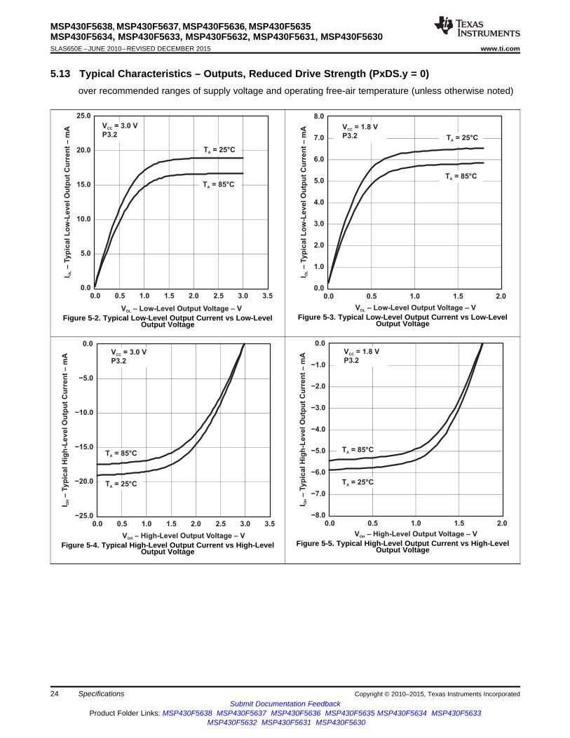
5.13 Typical Characteristics – Outputs, Reduced Drive Strength (PxDS.y = 0)over recommended ranges of supply voltage and operating free-air temperature (unless otherwise noted)
Figure 5-3. Typical Low-Level Output Current vs Low-LevelFigure 5-2. Typical Low-Level Output Current vs Low-LevelOutput VoltageOutput Voltage
Figure 5-5. Typical High-Level Output Current vs High-LevelFigure 5-4. Typical High-Level Output Current vs High-Level Output VoltageOutput Voltage
24 Specifications Copyright © 2010–2015, Texas Instruments IncorporatedSubmit Documentation Feedback
Product Folder Links: MSP430F5638 MSP430F5637 MSP430F5636 MSP430F5635 MSP430F5634 MSP430F5633MSP430F5632 MSP430F5631 MSP430F5630

−20
−16
−12
−8
−4
0
0.0 0.5 1.0 1.5 2.0
T = 25°CA
T = 85°CA
V = 1.8 V
P3.2CC
V – High-Level Output Voltage – VOH
I–
Ty
pic
al
Hig
h-L
ev
el
Ou
tpu
t C
urr
en
t–
mA
OH
−60.0
−55.0
−50.0
−45.0
−40.0
−35.0
−30.0
−25.0
−20.0
−15.0
−10.0
−5.0
0.0
0.0 0.5 1.0 1.5 2.0 2.5 3.0 3.5
T = 25°CA
T = 85°CA
V = 3.0 V
P3.2CC
V – High-Level Output Voltage – VOH
I–
Typ
ical H
igh
-Level O
utp
ut
Cu
rren
t–
mA
OH
0.0
5.0
10.0
15.0
20.0
25.0
30.0
35.0
40.0
45.0
50.0
55.0
60.0
0.0 0.5 1.0 1.5 2.0 2.5 3.0 3.5
T = 25°CA
T = 85°CA
V = 3.0 V
P3.2CC
V – Low-Level Output Voltage – VOL
I–
Ty
pic
al
Lo
w-L
ev
el
Ou
tpu
t C
urr
en
t–
mA
OL
0
4
8
12
16
20
24
0.0 0.5 1.0 1.5 2.0
T = 25°CA
T = 85°CA
V = 1.8 V
P3.2CC
V – Low-Level Output Voltage – VOL
I–
Typ
ical L
ow
-Level O
utp
ut
Cu
rren
t–
mA
OL
MSP430F5638, MSP430F5637, MSP430F5636, MSP430F5635MSP430F5634, MSP430F5633, MSP430F5632, MSP430F5631, MSP430F5630
www.ti.com SLAS650E –JUNE 2010–REVISED DECEMBER 2015
5.14 Typical Characteristics – Outputs, Full Drive Strength (PxDS.y = 1)over recommended ranges of supply voltage and operating free-air temperature (unless otherwise noted)
Figure 5-7. Typical Low-Level Output Current vs Low-LevelFigure 5-6. Typical Low-Level Output Current vs Low-LevelOutput VoltageOutput Voltage
Figure 5-8. Typical High-Level Output Current vs High-Level Figure 5-9. Typical High-Level Output Current vs High-LevelOutput Voltage Output Voltage
Copyright © 2010–2015, Texas Instruments Incorporated Specifications 25Submit Documentation Feedback
Product Folder Links: MSP430F5638 MSP430F5637 MSP430F5636 MSP430F5635 MSP430F5634 MSP430F5633MSP430F5632 MSP430F5631 MSP430F5630
MSP430F5638, MSP430F5637, MSP430F5636, MSP430F5635MSP430F5634, MSP430F5633, MSP430F5632, MSP430F5631, MSP430F5630SLAS650E –JUNE 2010–REVISED DECEMBER 2015 www.ti.com
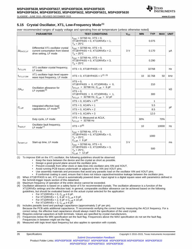
5.15 Crystal Oscillator, XT1, Low-Frequency Mode (1)
over recommended ranges of supply voltage and operating free-air temperature (unless otherwise noted)PARAMETER TEST CONDITIONS VCC MIN TYP MAX UNIT
fOSC = 32768 Hz, XTS = 0,XT1BYPASS = 0, XT1DRIVEx = 1, 0.075TA = 25°C
Differential XT1 oscillator crystal fOSC = 32768 Hz, XTS = 0,ΔIDVCC,LF current consumption from lowest XT1BYPASS = 0, XT1DRIVEx = 2, 3 V 0.170 µA
drive setting, LF mode TA = 25°CfOSC = 32768 Hz, XTS = 0,XT1BYPASS = 0, XT1DRIVEx = 3, 0.290TA = 25°C
XT1 oscillator crystal frequency,fXT1,LF0 XTS = 0, XT1BYPASS = 0 32768 HzLF modeXT1 oscillator logic-level square-fXT1,LF,SW XTS = 0, XT1BYPASS = 1 (2) (3) 10 32.768 50 kHzwave input frequency, LF mode
XTS = 0,XT1BYPASS = 0, XT1DRIVEx = 0, 210fXT1,LF = 32768 Hz, CL,eff = 6 pFOscillation allowance forOALF kΩLF crystals (4) XTS = 0,XT1BYPASS = 0, XT1DRIVEx = 1, 300fXT1,LF = 32768 Hz, CL,eff = 12 pFXTS = 0, XCAPx = 0 (6) 1XTS = 0, XCAPx = 1 5.5Integrated effective loadCL,eff pFcapacitance, LF mode (5) XTS = 0, XCAPx = 2 8.5XTS = 0, XCAPx = 3 12.0XTS = 0, Measured at ACLK,Duty cycle, LF mode 30% 70%fXT1,LF = 32768 Hz
Oscillator fault frequency,fFault,LF XTS = 0 (8) 10 10000 HzLF mode (7)
fOSC = 32768 Hz, XTS = 0,XT1BYPASS = 0, XT1DRIVEx = 0, 1000TA = 25°C,CL,eff = 6 pF
tSTART,LF Start-up time, LF mode 3 V msfOSC = 32768 Hz, XTS = 0,XT1BYPASS = 0, XT1DRIVEx = 3, 500TA = 25°C,CL,eff = 12 pF
(1) To improve EMI on the XT1 oscillator, the following guidelines should be observed.• Keep the trace between the device and the crystal as short as possible.• Design a good ground plane around the oscillator pins.• Prevent crosstalk from other clock or data lines into oscillator pins XIN and XOUT.• Avoid running PCB traces underneath or adjacent to the XIN and XOUT pins.• Use assembly materials and processes that avoid any parasitic load on the oscillator XIN and XOUT pins.• If conformal coating is used, ensure that it does not induce capacitive/resistive leakage between the oscillator pins.
(2) When XT1BYPASS is set, XT1 circuit is automatically powered down. Input signal is a digital square wave with parametrics defined inthe Schmitt-trigger Inputs section of this datasheet.
(3) Maximum frequency of operation of the entire device cannot be exceeded.(4) Oscillation allowance is based on a safety factor of 5 for recommended crystals. The oscillation allowance is a function of the
XT1DRIVEx settings and the effective load. In general, comparable oscillator allowance can be achieved based on the followingguidelines, but should be evaluated based on the actual crystal selected for the application:
• For XT1DRIVEx = 0, CL,eff ≤ 6 pF.• For XT1DRIVEx = 1, 6 pF ≤ CL,eff ≤ 9 pF.• For XT1DRIVEx = 2, 6 pF ≤ CL,eff ≤ 10 pF.• For XT1DRIVEx = 3, CL,eff ≥ 6 pF.
(5) Includes parasitic bond and package capacitance (approximately 2 pF per pin).Because the PCB adds additional capacitance, TI recommends verifying the correct load by measuring the ACLK frequency. For acorrect setup, the effective load capacitance should always match the specification of the used crystal.
(6) Requires external capacitors at both terminals. Values are specified by crystal manufacturers.(7) Frequencies below the MIN specification set the fault flag. Frequencies above the MAX specification do not set the fault flag.
Frequencies in between might set the flag.(8) Measured with logic-level input frequency but also applies to operation with crystals.
26 Specifications Copyright © 2010–2015, Texas Instruments IncorporatedSubmit Documentation Feedback
Product Folder Links: MSP430F5638 MSP430F5637 MSP430F5636 MSP430F5635 MSP430F5634 MSP430F5633MSP430F5632 MSP430F5631 MSP430F5630

MSP430F5638, MSP430F5637, MSP430F5636, MSP430F5635MSP430F5634, MSP430F5633, MSP430F5632, MSP430F5631, MSP430F5630
www.ti.com SLAS650E –JUNE 2010–REVISED DECEMBER 2015
5.16 Crystal Oscillator, XT2over recommended ranges of supply voltage and operating free-air temperature (unless otherwise noted) (1) (2)
PARAMETER TEST CONDITIONS VCC MIN TYP MAX UNITfOSC = 4 MHz, XT2OFF = 0,XT2BYPASS = 0, XT2DRIVEx = 0, 200TA = 25°CfOSC = 12 MHz, XT2OFF = 0,XT2BYPASS = 0, XT2DRIVEx = 1, 260TA = 25°CXT2 oscillator crystal currentIDVCC,XT2 3 V µAconsumption fOSC = 20 MHz, XT2OFF = 0,XT2BYPASS = 0, XT2DRIVEx = 2, 325TA = 25°CfOSC = 32 MHz, XT2OFF = 0,XT2BYPASS = 0, XT2DRIVEx = 3, 450TA = 25°C
XT2 oscillator crystal frequency,fXT2,HF0 XT2DRIVEx = 0, XT2BYPASS = 0 (3) 4 8 MHzmode 0XT2 oscillator crystal frequency,fXT2,HF1 XT2DRIVEx = 1, XT2BYPASS = 0 (3) 8 16 MHzmode 1XT2 oscillator crystal frequency,fXT2,HF2 XT2DRIVEx = 2, XT2BYPASS = 0 (3) 16 24 MHzmode 2XT2 oscillator crystal frequency,fXT2,HF3 XT2DRIVEx = 3, XT2BYPASS = 0 (3) 24 32 MHzmode 3XT2 oscillator logic-level square-fXT2,HF,SW XT2BYPASS = 1 (4) (3) 0.7 32 MHzwave input frequency
XT2DRIVEx = 0, XT2BYPASS = 0, 450fXT2,HF0 = 6 MHz, CL,eff = 15 pFXT2DRIVEx = 1, XT2BYPASS = 0, 320fXT2,HF1 = 12 MHz, CL,eff = 15 pFOscillation allowance forOAHF ΩHF crystals (5) XT2DRIVEx = 2, XT2BYPASS = 0, 200fXT2,HF2 = 20 MHz, CL,eff = 15 pFXT2DRIVEx = 3, XT2BYPASS = 0, 200fXT2,HF3 = 32 MHz, CL,eff = 15 pFfOSC = 6 MHzXT2BYPASS = 0, XT2DRIVEx = 0, 0.5TA = 25°C, CL,eff = 15 pF
tSTART,HF Start-up time 3 V msfOSC = 20 MHzXT2BYPASS = 0, XT2DRIVEx = 3, 0.3TA = 25°C, CL,eff = 15 pF
Integrated effective loadCL,eff 1 pFcapacitance, HF mode (6) (1)
Duty cycle Measured at ACLK, fXT2,HF2 = 20 MHz 40% 50% 60%fFault,HF Oscillator fault frequency (7) XT2BYPASS = 1 (8) 30 300 kHz
(1) Requires external capacitors at both terminals. Values are specified by crystal manufacturers.(2) To improve EMI on the XT2 oscillator the following guidelines should be observed.
• Keep the traces between the device and the crystal as short as possible.• Design a good ground plane around the oscillator pins.• Prevent crosstalk from other clock or data lines into oscillator pins XT2IN and XT2OUT.• Avoid running PCB traces underneath or adjacent to the XT2IN and XT2OUT pins.• Use assembly materials and processes that avoid any parasitic load on the oscillator XT2IN and XT2OUT pins.• If conformal coating is used, ensure that it does not induce capacitive/resistive leakage between the oscillator pins.
(3) Maximum frequency of operation of the entire device cannot be exceeded.(4) When XT2BYPASS is set, the XT2 circuit is automatically powered down.(5) Oscillation allowance is based on a safety factor of 5 for recommended crystals.(6) Includes parasitic bond and package capacitance (approximately 2 pF per pin).
Because the PCB adds additional capacitance, TI recommends verifying the correct load by measuring the ACLK frequency. For acorrect setup, the effective load capacitance should always match the specification of the used crystal.
(7) Frequencies below the MIN specification set the fault flag. Frequencies above the MAX specification do not set the fault flag.Frequencies in between might set the flag.
(8) Measured with logic-level input frequency but also applies to operation with crystals.
Copyright © 2010–2015, Texas Instruments Incorporated Specifications 27Submit Documentation Feedback
Product Folder Links: MSP430F5638 MSP430F5637 MSP430F5636 MSP430F5635 MSP430F5634 MSP430F5633MSP430F5632 MSP430F5631 MSP430F5630
MSP430F5638, MSP430F5637, MSP430F5636, MSP430F5635MSP430F5634, MSP430F5633, MSP430F5632, MSP430F5631, MSP430F5630SLAS650E –JUNE 2010–REVISED DECEMBER 2015 www.ti.com
5.17 Internal Very-Low-Power Low-Frequency Oscillator (VLO)over recommended ranges of supply voltage and operating free-air temperature (unless otherwise noted)
PARAMETER TEST CONDITIONS VCC MIN TYP MAX UNITfVLO VLO frequency Measured at ACLK 1.8 V to 3.6 V 6 9.4 14 kHzdfVLO/dT VLO frequency temperature drift Measured at ACLK (1) 1.8 V to 3.6 V 0.5 %/°CdfVLO/dVCC VLO frequency supply voltage drift Measured at ACLK (2) 1.8 V to 3.6 V 4 %/V
Duty cycle Measured at ACLK 1.8 V to 3.6 V 40% 50% 60%
(1) Calculated using the box method: (MAX(–40°C to +85°C) – MIN(–40°C to +85°C)) / MIN(–40°C to +85°C) / (85°C – (–40°C))(2) Calculated using the box method: (MAX(1.8 V to 3.6 V) – MIN(1.8 V to 3.6 V)) / MIN(1.8 V to 3.6 V) / (3.6 V – 1.8 V)
5.18 Internal Reference, Low-Frequency Oscillator (REFO)over recommended ranges of supply voltage and operating free-air temperature (unless otherwise noted)
PARAMETER TEST CONDITIONS VCC MIN TYP MAX UNITREFO oscillator currentIREFO TA = 25°C 1.8 V to 3.6 V 3 µAconsumptionREFO frequency calibrated Measured at ACLK 1.8 V to 3.6 V 32768 Hz
fREFO Full temperature range 1.8 V to 3.6 V ±3.5%REFO absolute tolerancecalibrated TA = 25°C 3 V ±1.5%
dfREFO/dT REFO frequency temperature drift Measured at ACLK (1) 1.8 V to 3.6 V 0.01 %/°CREFO frequency supply voltagedfREFO/dVCC Measured at ACLK (2) 1.8 V to 3.6 V 1.0 %/VdriftDuty cycle Measured at ACLK 1.8 V to 3.6 V 40% 50% 60%
tSTART REFO start-up time 40%/60% duty cycle 1.8 V to 3.6 V 25 µs
(1) Calculated using the box method: (MAX(–40°C to +85°C) – MIN(–40°C to +85°C)) / MIN(–40°C to +85°C) / (85°C – (–40°C))(2) Calculated using the box method: (MAX(1.8 V to 3.6 V) – MIN(1.8 V to 3.6 V)) / MIN(1.8 V to 3.6 V) / (3.6 V – 1.8 V)
28 Specifications Copyright © 2010–2015, Texas Instruments IncorporatedSubmit Documentation Feedback
Product Folder Links: MSP430F5638 MSP430F5637 MSP430F5636 MSP430F5635 MSP430F5634 MSP430F5633MSP430F5632 MSP430F5631 MSP430F5630

0 1 2 3 4 5 6 7
Typical DCO Frequency, V = 3.0 V,T = 25°CCC A
DCORSEL
100
10
1
0.1
f– M
Hz
DC
O
DCOx = 31
DCOx = 0
MSP430F5638, MSP430F5637, MSP430F5636, MSP430F5635MSP430F5634, MSP430F5633, MSP430F5632, MSP430F5631, MSP430F5630
www.ti.com SLAS650E –JUNE 2010–REVISED DECEMBER 2015
5.19 DCO Frequencyover recommended ranges of supply voltage and operating free-air temperature (unless otherwise noted)
PARAMETER TEST CONDITIONS MIN TYP MAX UNITfDCO(0,0) DCO frequency (0, 0) DCORSELx = 0, DCOx = 0, MODx = 0 0.07 0.20 MHzfDCO(0,31) DCO frequency (0, 31) DCORSELx = 0, DCOx = 31, MODx = 0 0.70 1.70 MHzfDCO(1,0) DCO frequency (1, 0) DCORSELx = 1, DCOx = 0, MODx = 0 0.15 0.36 MHzfDCO(1,31) DCO frequency (1, 31) DCORSELx = 1, DCOx = 31, MODx = 0 1.47 3.45 MHzfDCO(2,0) DCO frequency (2, 0) DCORSELx = 2, DCOx = 0, MODx = 0 0.32 0.75 MHzfDCO(2,31) DCO frequency (2, 31) DCORSELx = 2, DCOx = 31, MODx = 0 3.17 7.38 MHzfDCO(3,0) DCO frequency (3, 0) DCORSELx = 3, DCOx = 0, MODx = 0 0.64 1.51 MHzfDCO(3,31) DCO frequency (3, 31) DCORSELx = 3, DCOx = 31, MODx = 0 6.07 14.0 MHzfDCO(4,0) DCO frequency (4, 0) DCORSELx = 4, DCOx = 0, MODx = 0 1.3 3.2 MHzfDCO(4,31) DCO frequency (4, 31) DCORSELx = 4, DCOx = 31, MODx = 0 12.3 28.2 MHzfDCO(5,0) DCO frequency (5, 0) DCORSELx = 5, DCOx = 0, MODx = 0 2.5 6.0 MHzfDCO(5,31) DCO frequency (5, 31) DCORSELx = 5, DCOx = 31, MODx = 0 23.7 54.1 MHzfDCO(6,0) DCO frequency (6, 0) DCORSELx = 6, DCOx = 0, MODx = 0 4.6 10.7 MHzfDCO(6,31) DCO frequency (6, 31) DCORSELx = 6, DCOx = 31, MODx = 0 39.0 88.0 MHzfDCO(7,0) DCO frequency (7, 0) DCORSELx = 7, DCOx = 0, MODx = 0 8.5 19.6 MHzfDCO(7,31) DCO frequency (7, 31) DCORSELx = 7, DCOx = 31, MODx = 0 60 135 MHz
Frequency step between rangeSDCORSEL SRSEL = fDCO(DCORSEL+1,DCO)/fDCO(DCORSEL,DCO) 1.2 2.3 ratioDCORSEL and DCORSEL + 1Frequency step between tapSDCO SDCO = fDCO(DCORSEL,DCO+1)/fDCO(DCORSEL,DCO) 1.02 1.12 ratioDCO and DCO + 1Duty cycle Measured at SMCLK 40% 50% 60%
dfDCO/dT DCO frequency temperature drift fDCO = 1 MHz 0.1 %/°CdfDCO/dVCC DCO frequency voltage drift fDCO = 1 MHz 1.9 %/V
Figure 5-10. Typical DCO frequency
Copyright © 2010–2015, Texas Instruments Incorporated Specifications 29Submit Documentation Feedback
Product Folder Links: MSP430F5638 MSP430F5637 MSP430F5636 MSP430F5635 MSP430F5634 MSP430F5633MSP430F5632 MSP430F5631 MSP430F5630

MSP430F5638, MSP430F5637, MSP430F5636, MSP430F5635MSP430F5634, MSP430F5633, MSP430F5632, MSP430F5631, MSP430F5630SLAS650E –JUNE 2010–REVISED DECEMBER 2015 www.ti.com
5.20 PMM, Brownout Reset (BOR)over recommended ranges of supply voltage and operating free-air temperature (unless otherwise noted)
PARAMETER TEST CONDITIONS MIN TYP MAX UNITBORH on voltage,V(DVCC_BOR_IT–) | dDVCC/dt | < 3 V/s 1.45 VDVCC falling levelBORH off voltage,V(DVCC_BOR_IT+) | dDVCC/dt | < 3 V/s 0.80 1.30 1.50 VDVCC rising level
V(DVCC_BOR_hys) BORH hysteresis 60 250 mVPulse length required at
tRESET RST/NMI pin to accept a 2 µsreset
5.21 PMM, Core Voltageover recommended ranges of supply voltage and operating free-air temperature (unless otherwise noted)
PARAMETER TEST CONDITIONS MIN TYP MAX UNITCore voltage, activeVCORE3(AM) 2.4 V ≤ DVCC ≤ 3.6 V, 0 mA ≤ I(VCORE) ≤ 21 mA 1.90 Vmode, PMMCOREV = 3Core voltage, activeVCORE2(AM) 2.2 V ≤ DVCC ≤ 3.6 V, 0 mA ≤ I(VCORE) ≤ 21 mA 1.80 Vmode, PMMCOREV = 2Core voltage, activeVCORE1(AM) 2 V ≤ DVCC ≤ 3.6 V, 0 mA ≤ I(VCORE) ≤ 17 mA 1.60 Vmode, PMMCOREV = 1Core voltage, activeVCORE0(AM) 1.8 V ≤ DVCC ≤ 3.6 V, 0 mA ≤ I(VCORE) ≤ 13 mA 1.40 Vmode, PMMCOREV = 0Core voltage, low-currentVCORE3(LPM) 2.4 V ≤ DVCC ≤ 3.6 V, 0 µA ≤ I(VCORE) ≤ 30 µA 1.94 Vmode, PMMCOREV = 3Core voltage, low-currentVCORE2(LPM) 2.2 V ≤ DVCC ≤ 3.6 V, 0 µA ≤ I(VCORE) ≤ 30 µA 1.84 Vmode, PMMCOREV = 2Core voltage, low-currentVCORE1(LPM) 2 V ≤ DVCC ≤ 3.6 V, 0 µA ≤ I(VCORE) ≤ 30 µA 1.64 Vmode, PMMCOREV = 1Core voltage, low-currentVCORE0(LPM) 1.8 V ≤ DVCC ≤ 3.6 V, 0 µA ≤ I(VCORE) ≤ 30 µA 1.44 Vmode, PMMCOREV = 0
30 Specifications Copyright © 2010–2015, Texas Instruments IncorporatedSubmit Documentation Feedback
Product Folder Links: MSP430F5638 MSP430F5637 MSP430F5636 MSP430F5635 MSP430F5634 MSP430F5633MSP430F5632 MSP430F5631 MSP430F5630

MSP430F5638, MSP430F5637, MSP430F5636, MSP430F5635MSP430F5634, MSP430F5633, MSP430F5632, MSP430F5631, MSP430F5630
www.ti.com SLAS650E –JUNE 2010–REVISED DECEMBER 2015
5.22 PMM, SVS High Sideover recommended ranges of supply voltage and operating free-air temperature (unless otherwise noted)
PARAMETER TEST CONDITIONS MIN TYP MAX UNITSVSHE = 0, DVCC = 3.6 V 0
nAI(SVSH) SVS current consumption SVSHE = 1, DVCC = 3.6 V, SVSHFP = 0 200
SVSHE = 1, DVCC = 3.6 V, SVSHFP = 1 2.0 µASVSHE = 1, SVSHRVL = 0 1.59 1.64 1.69SVSHE = 1, SVSHRVL = 1 1.79 1.84 1.91
V(SVSH_IT–) SVSH on voltage level (1) VSVSHE = 1, SVSHRVL = 2 1.98 2.04 2.11SVSHE = 1, SVSHRVL = 3 2.10 2.16 2.23SVSHE = 1, SVSMHRRL = 0 1.62 1.74 1.81SVSHE = 1, SVSMHRRL = 1 1.88 1.94 2.01SVSHE = 1, SVSMHRRL = 2 2.07 2.14 2.21SVSHE = 1, SVSMHRRL = 3 2.20 2.26 2.33
V(SVSH_IT+) SVSH off voltage level (1) VSVSHE = 1, SVSMHRRL = 4 2.32 2.40 2.48SVSHE = 1, SVSMHRRL = 5 2.56 2.70 2.84SVSHE = 1, SVSMHRRL = 6 2.85 3.00 3.15SVSHE = 1, SVSMHRRL = 7 2.85 3.00 3.15SVSHE = 1, dVDVCC/dt = 10 mV/µs, SVSHFP = 1 2.5
tpd(SVSH) SVSH propagation delay µsSVSHE = 1, dVDVCC/dt = 1 mV/µs, SVSHFP = 0 20SVSHE = 0→1, SVSHFP = 1 12.5
t(SVSH) SVSH on or off delay time µsSVSHE = 0→1, SVSHFP = 0 100
dVDVCC/dt DVCC rise time 0 1000 V/s
(1) The SVSH settings available depend on the VCORE (PMMCOREVx) setting. See the Power Management Module and Supply VoltageSupervisor chapter in the MSP430x5xx and MSP430x6xx Family User's Guide (SLAU208) on recommended settings and usage.
5.23 PMM, SVM High Sideover recommended ranges of supply voltage and operating free-air temperature (unless otherwise noted)
PARAMETER TEST CONDITIONS MIN TYP MAX UNITSVMHE = 0, DVCC = 3.6 V 0
nAI(SVMH) SVMH current consumption SVMHE = 1, DVCC = 3.6 V, SVMHFP = 0 200
SVMHE = 1, DVCC = 3.6 V, SVMHFP = 1 2.0 µASVMHE = 1, SVSMHRRL = 0 1.65 1.74 1.86SVMHE = 1, SVSMHRRL = 1 1.85 1.94 2.02SVMHE = 1, SVSMHRRL = 2 2.02 2.14 2.22SVMHE = 1, SVSMHRRL = 3 2.18 2.26 2.35
V(SVMH) SVMH on or off voltage level (1) SVMHE = 1, SVSMHRRL = 4 2.32 2.40 2.48 VSVMHE = 1, SVSMHRRL = 5 2.56 2.70 2.84SVMHE = 1, SVSMHRRL = 6 2.85 3.00 3.15SVMHE = 1, SVSMHRRL = 7 2.85 3.00 3.15SVMHE = 1, SVMHOVPE = 1 3.75SVMHE = 1, dVDVCC/dt = 10 mV/µs, SVMHFP = 1 2.5
tpd(SVMH) SVMH propagation delay µsSVMHE = 1, dVDVCC/dt = 1 mV/µs, SVMHFP = 0 20SVMHE = 0→1, SVSMFP = 1 12.5
t(SVMH) SVMH on or off delay time µsSVMHE = 0→1, SVMHFP = 0 100
(1) The SVMH settings available depend on the VCORE (PMMCOREVx) setting. See the Power Management Module and Supply VoltageSupervisor chapter in the MSP430x5xx and MSP430x6xx Family User's Guide (SLAU208) on recommended settings and usage.
Copyright © 2010–2015, Texas Instruments Incorporated Specifications 31Submit Documentation Feedback
Product Folder Links: MSP430F5638 MSP430F5637 MSP430F5636 MSP430F5635 MSP430F5634 MSP430F5633MSP430F5632 MSP430F5631 MSP430F5630

MSP430F5638, MSP430F5637, MSP430F5636, MSP430F5635MSP430F5634, MSP430F5633, MSP430F5632, MSP430F5631, MSP430F5630SLAS650E –JUNE 2010–REVISED DECEMBER 2015 www.ti.com
5.24 PMM, SVS Low Sideover recommended ranges of supply voltage and operating free-air temperature (unless otherwise noted)
PARAMETER TEST CONDITIONS MIN TYP MAX UNITSVSLE = 0, PMMCOREV = 2 0
nAI(SVSL) SVSL current consumption SVSLE = 1, PMMCOREV = 2, SVSLFP = 0 200
SVSLE = 1, PMMCOREV = 2, SVSLFP = 1 2.0 µASVSLE = 1, dVCORE/dt = 10 mV/µs, SVSLFP = 1 2.5
tpd(SVSL) SVSL propagation delay µsSVSLE = 1, dVCORE/dt = 1 mV/µs, SVSLFP = 0 20SVSLE = 0→1, SVSLFP = 1 12.5
t(SVSL) SVSL on/off delay time µsSVSLE = 0→1, SVSLFP = 0 100
5.25 PMM, SVM Low Sideover recommended ranges of supply voltage and operating free-air temperature (unless otherwise noted)
PARAMETER TEST CONDITIONS MIN TYP MAX UNITSVMLE = 0, PMMCOREV = 2 0
nAI(SVML) SVML current consumption SVMLE = 1, PMMCOREV = 2, SVMLFP = 0 200
SVMLE = 1, PMMCOREV = 2, SVMLFP = 1 2.0 µASVMLE = 1, dVCORE/dt = 10 mV/µs, SVMLFP = 1 2.5
tpd(SVML) SVML propagation delay µsSVMLE = 1, dVCORE/dt = 1 mV/µs, SVMLFP = 0 20SVMLE = 0→1, SVMLFP = 1 12.5
t(SVML) SVML on or off delay time µsSVMLE = 0→1, SVMLFP = 0 100
5.26 Wake-up Times From Low-Power Modes and Resetover recommended ranges of supply voltage and operating free-air temperature (unless otherwise noted)
PARAMETER TEST CONDITIONS MIN TYP MAX UNITfMCLK ≥ 4 MHz 3 6.5Wake-up time from LPM2, PMMCOREV = SVSMLRRL = n
tWAKE-UP-FAST LPM3, or LPM4 to active (where n = 0, 1, 2, or 3), µs1 MHz < fMCLK < 4 8.0mode (1) SVSLFP = 1 4 MHzWake-up time from LPM2, PMMCOREV = SVSMLRRL = n
tWAKE-UP-SLOW LPM3 or LPM4 to active (where n = 0, 1, 2, or 3), 150 165 µsmode (2) SVSLFP = 0Wake-up time from LPM3.5 ortWAKE-UP-LPM5 2 3 msLPM4.5 to active mode (3)
Wake-up time from RST ortWAKE-UP-RESET 2 3 msBOR event to active mode (3)
(1) This value represents the time from the wake-up event to the first active edge of MCLK. The wake-up time depends on the performancemode of the low-side supervisor (SVSL) and low-side monitor (SVML). Fastest wake-up times are possible with SVSL and SVML in fullperformance mode or disabled when operating in AM, LPM0, and LPM1. Various options are available for SVSL and SVML whileoperating in LPM2, LPM3, and LPM4. See the Power Management Module and Supply Voltage Supervisor chapter in the MSP430x5xxand MSP430x6xx Family User's Guide (SLAU208).
(2) This value represents the time from the wake-up event to the first active edge of MCLK. The wake-up time depends on the performancemode of the low-side supervisor (SVSL) and low-side monitor (SVML). In this case, the SVSL and SVML are in normal mode (lowcurrent) mode when operating in AM, LPM0, and LPM1. Various options are available for SVSL and SVML while operating in LPM2,LPM3, and LPM4. See the Power Management Module and Supply Voltage Supervisor chapter in the MSP430x5xx and MSP430x6xxFamily User's Guide (SLAU208).
(3) This value represents the time from the wake-up event to the reset vector execution.
32 Specifications Copyright © 2010–2015, Texas Instruments IncorporatedSubmit Documentation Feedback
Product Folder Links: MSP430F5638 MSP430F5637 MSP430F5636 MSP430F5635 MSP430F5634 MSP430F5633MSP430F5632 MSP430F5631 MSP430F5630
MSP430F5638, MSP430F5637, MSP430F5636, MSP430F5635MSP430F5634, MSP430F5633, MSP430F5632, MSP430F5631, MSP430F5630
www.ti.com SLAS650E –JUNE 2010–REVISED DECEMBER 2015
5.27 Timer_A, Timers TA0, TA1, and TA2over recommended ranges of supply voltage and operating free-air temperature (unless otherwise noted)
PARAMETER TEST CONDITIONS VCC MIN MAX UNITInternal: SMCLK, ACLK
fTA Timer_A input clock frequency External: TACLK 1.8 V, 3 V 20 MHzDuty cycle = 50% ±10%All capture inputs,
tTA,cap Timer_A capture timing Minimum pulse duration required for 1.8 V, 3 V 20 nscapture
5.28 Timer_B, Timer TB0over recommended ranges of supply voltage and operating free-air temperature (unless otherwise noted)
PARAMETER TEST CONDITIONS VCC MIN MAX UNITInternal: SMCLK, ACLK
fTB Timer_B input clock frequency External: TBCLK 1.8 V, 3 V 20 MHzDuty cycle = 50% ±10%All capture inputs,
tTB,cap Timer_B capture timing Minimum pulse duration required for 1.8 V, 3 V 20 nscapture
5.29 Battery Backupover operating free-air temperature range (unless otherwise noted)
PARAMETER TEST CONDITIONS VCC MIN TYP MAX UNITTA = –40°C 0.43
VBAT = 1.7 V, TA = 25°C 0.52DVCC not connected,
TA = 60°C 0.58RTC runningTA = 85°C 0.64TA = –40°C 0.50
VBAT = 2.2 V, TA = 25°C 0.59Current into VBAT terminal if noIVBAT DVCC not connected, µAprimary battery is connected TA = 60°C 0.64RTC runningTA = 85°C 0.71TA = –40°C 0.68
VBAT = 3 V, TA = 25°C 0.75DVCC not connected,
TA = 60°C 0.79RTC runningTA = 85°C 0.86General VSVSH_IT-
SVSHRL = 0 1.59 1.69VSWITCH Switch-over level (VCC to VBAT) CVCC = 4.7 µF SVSHRL = 1 1.79 1.91 V
SVSHRL = 2 1.98 2.11SVSHRL = 3 2.10 2.23
ON-resistance of switchRON_VBAT VBAT = 1.8 V 0 V 0.35 1 kΩbetween VBAT and VBAK1.8 V 0.6 ±5%
VBAT to ADC input channel 12:VBAT3 3 V 1.0 ±5% VVBAT divided, VBAT3 = VBAT/33.6 V 1.2 ±5%
tSample, VBAT to ADC: Sampling time ADC12ON = 1, 1000 nsVBAT3 required if VBAT3 selected Error of conversion result ≤ 1 LSBVCHVx Charger end voltage CHVx = 2 2.65 2.7 2.9 V
CHCx = 1 5RCHARGE Charge limiting resistor CHCx = 2 10 kΩ
CHCx = 3 20
Copyright © 2010–2015, Texas Instruments Incorporated Specifications 33Submit Documentation Feedback
Product Folder Links: MSP430F5638 MSP430F5637 MSP430F5636 MSP430F5635 MSP430F5634 MSP430F5633MSP430F5632 MSP430F5631 MSP430F5630

MSP430F5638, MSP430F5637, MSP430F5636, MSP430F5635MSP430F5634, MSP430F5633, MSP430F5632, MSP430F5631, MSP430F5630SLAS650E –JUNE 2010–REVISED DECEMBER 2015 www.ti.com
5.30 USCI (UART Mode)over recommended ranges of supply voltage and operating free-air temperature (unless otherwise noted)
PARAMETER TEST CONDITIONS VCC MIN MAX UNITInternal: SMCLK, ACLK
fUSCI USCI input clock frequency External: UCLK fSYSTEM MHzDuty cycle = 50% ±10%
BITCLK clock frequencyfBITCLK 1 MHz(equals baud rate in MBaud)2.2 V 50 600
tτ UART receive deglitch time (1) ns3 V 50 600
(1) Pulses on the UART receive input (UCxRX) shorter than the UART receive deglitch time are suppressed. To ensure that pulses arecorrectly recognized their width should exceed the maximum specification of the deglitch time.
5.31 USCI (SPI Master Mode)over recommended ranges of supply voltage and operating free-air temperature (unless otherwise noted) (1)
(see Figure 5-11 and Figure 5-12)PARAMETER TEST CONDITIONS VCC MIN MAX UNIT
SMCLK, ACLK,fUSCI USCI input clock frequency fSYSTEM MHzDuty cycle = 50% ±10%1.8 V 55
PMMCOREV = 03 V 38
tSU,MI SOMI input data setup time ns2.4 V 30
PMMCOREV = 33 V 25
1.8 V 0PMMCOREV = 0
3 V 0tHD,MI SOMI input data hold time ns
2.4 V 0PMMCOREV = 3
3 V 0UCLK edge to SIMO valid, 1.8 V 20CL = 20 pF,
3 V 18PMMCOREV = 0tVALID,MO SIMO output data valid time (2) ns2.4 V 16UCLK edge to SIMO valid,
CL = 20 pF, PMMCOREV = 3 3 V 151.8 V –10
CL = 20 pF, PMMCOREV = 03 V –8
tHD,MO SIMO output data hold time (3) ns2.4 V –10
CL = 20 pF, PMMCOREV = 33 V –8
(1) fUCxCLK = 1/2tLO/HI with tLO/HI ≥ max(tVALID,MO(USCI) + tSU,SI(Slave), tSU,MI(USCI) + tVALID,SO(Slave)).For the slave parameters tSU,SI(Slave) and tVALID,SO(Slave), see the SPI parameters of the attached slave.
(2) Specifies the time to drive the next valid data to the SIMO output after the output changing UCLK clock edge. See the timing diagramsin Figure 5-11 and Figure 5-12.
(3) Specifies how long data on the SIMO output is valid after the output changing UCLK clock edge. Negative values indicate that the dataon the SIMO output can become invalid before the output changing clock edge observed on UCLK. See the timing diagrams in Figure 5-11 and Figure 5-12.
34 Specifications Copyright © 2010–2015, Texas Instruments IncorporatedSubmit Documentation Feedback
Product Folder Links: MSP430F5638 MSP430F5637 MSP430F5636 MSP430F5635 MSP430F5634 MSP430F5633MSP430F5632 MSP430F5631 MSP430F5630
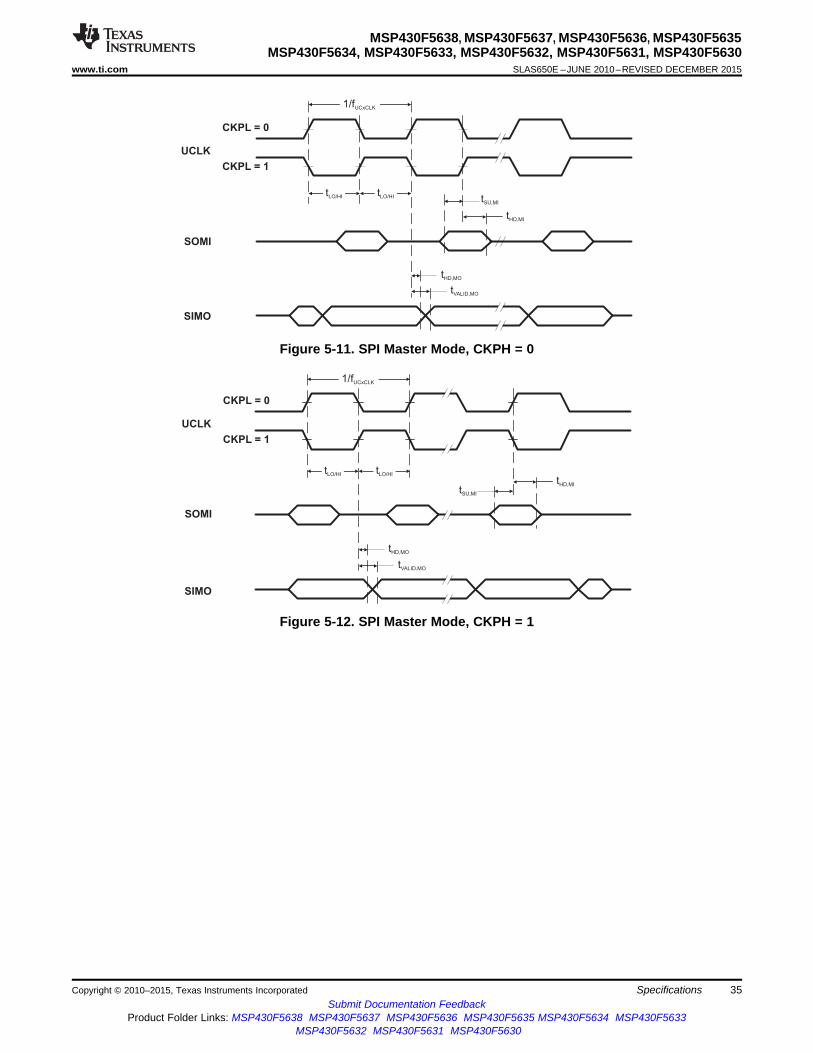
tSU,MI
tHD,MI
UCLK
SOMI
SIMO
tVALID,MO
CKPL = 0
CKPL = 1
1/fUCxCLK
tHD,MO
tLO/HI tLO/HI
tSU,MI
tHD,MI
UCLK
SOMI
SIMO
tVALID,MO
tHD,MO
CKPL = 0
CKPL = 1
tLO/HI tLO/HI
1/fUCxCLK
MSP430F5638, MSP430F5637, MSP430F5636, MSP430F5635MSP430F5634, MSP430F5633, MSP430F5632, MSP430F5631, MSP430F5630
www.ti.com SLAS650E –JUNE 2010–REVISED DECEMBER 2015
Figure 5-11. SPI Master Mode, CKPH = 0
Figure 5-12. SPI Master Mode, CKPH = 1
Copyright © 2010–2015, Texas Instruments Incorporated Specifications 35Submit Documentation Feedback
Product Folder Links: MSP430F5638 MSP430F5637 MSP430F5636 MSP430F5635 MSP430F5634 MSP430F5633MSP430F5632 MSP430F5631 MSP430F5630

MSP430F5638, MSP430F5637, MSP430F5636, MSP430F5635MSP430F5634, MSP430F5633, MSP430F5632, MSP430F5631, MSP430F5630SLAS650E –JUNE 2010–REVISED DECEMBER 2015 www.ti.com
5.32 USCI (SPI Slave Mode)over recommended ranges of supply voltage and operating free-air temperature (unless otherwise noted) (1)
(see Figure 5-13 and Figure 5-14)PARAMETER TEST CONDITIONS VCC MIN MAX UNIT
1.8 V 11PMMCOREV = 0
3 V 8tSTE,LEAD STE lead time, STE low to clock ns
2.4 V 7PMMCOREV = 3
3 V 61.8 V 3
PMMCOREV = 03 V 3
tSTE,LAG STE lag time, Last clock to STE high ns2.4 V 3
PMMCOREV = 33 V 3
1.8 V 66PMMCOREV = 0
3 V 50tSTE,ACC STE access time, STE low to SOMI data out ns
2.4 V 36PMMCOREV = 3
3 V 301.8 V 30
PMMCOREV = 03 V 23STE disable time, STE high to SOMI hightSTE,DIS nsimpedance 2.4 V 16
PMMCOREV = 33 V 13
1.8 V 5PMMCOREV = 0
3 V 5tSU,SI SIMO input data setup time ns
2.4 V 2PMMCOREV = 3
3 V 21.8 V 5
PMMCOREV = 03 V 5
tHD,SI SIMO input data hold time ns2.4 V 5
PMMCOREV = 33 V 5
UCLK edge to SOMI valid, 1.8 V 76CL = 20 pF,
3 V 60PMMCOREV = 0tVALID,SO SOMI output data valid time (2) ns
UCLK edge to SOMI valid, 2.4 V 44CL = 20 pF,
3 V 40PMMCOREV = 31.8 V 18CL = 20 pF,
PMMCOREV = 0 3 V 12tHD,SO SOMI output data hold time (3) ns
2.4 V 10CL = 20 pF,PMMCOREV = 3 3 V 8
(1) fUCxCLK = 1/2tLO/HI with tLO/HI ≥ max(tVALID,MO(Master) + tSU,SI(USCI), tSU,MI(Master) + tVALID,SO(USCI)).For the master parameters tSU,MI(Master) and tVALID,MO(Master), see the SPI parameters of the attached slave.
(2) Specifies the time to drive the next valid data to the SOMI output after the output changing UCLK clock edge. See the timing diagramsin Figure 5-13 and Figure 5-14.
(3) Specifies how long data on the SOMI output is valid after the output changing UCLK clock edge. See the timing diagrams in Figure 5-13and Figure 5-14.
36 Specifications Copyright © 2010–2015, Texas Instruments IncorporatedSubmit Documentation Feedback
Product Folder Links: MSP430F5638 MSP430F5637 MSP430F5636 MSP430F5635 MSP430F5634 MSP430F5633MSP430F5632 MSP430F5631 MSP430F5630

STE
UCLK
CKPL = 0
CKPL = 1
SOMI
SIMO
tSU,SI
tHD,SI
tVALID,SO
tSTE,LEAD
1/fUCxCLK
tSTE,LAG
tSTE,DIStSTE,ACC
tHD,MO
tLO/HI tLO/HI
STE
UCLK
CKPL = 0
CKPL = 1
SOMI
SIMO
tSU,SI
tHD,SI
tVALID,SO
tSTE,LEAD
1/fUCxCLK
tLO/HI tLO/HI
tSTE,LAG
tSTE,DIStSTE,ACC
tHD,SO
MSP430F5638, MSP430F5637, MSP430F5636, MSP430F5635MSP430F5634, MSP430F5633, MSP430F5632, MSP430F5631, MSP430F5630
www.ti.com SLAS650E –JUNE 2010–REVISED DECEMBER 2015
Figure 5-13. SPI Slave Mode, CKPH = 0
Figure 5-14. SPI Slave Mode, CKPH = 1
Copyright © 2010–2015, Texas Instruments Incorporated Specifications 37Submit Documentation Feedback
Product Folder Links: MSP430F5638 MSP430F5637 MSP430F5636 MSP430F5635 MSP430F5634 MSP430F5633MSP430F5632 MSP430F5631 MSP430F5630

SDA
SCL
tHD,DAT
tSU,DAT
tHD,STA
tHIGHtLOW
tBUFtHD,STAtSU,STA
tSP
tSU,STO
MSP430F5638, MSP430F5637, MSP430F5636, MSP430F5635MSP430F5634, MSP430F5633, MSP430F5632, MSP430F5631, MSP430F5630SLAS650E –JUNE 2010–REVISED DECEMBER 2015 www.ti.com
5.33 USCI (I2C Mode)over recommended ranges of supply voltage and operating free-air temperature (unless otherwise noted) (see Figure 5-15)
PARAMETER TEST CONDITIONS VCC MIN MAX UNITInternal: SMCLK, ACLK
fUSCI USCI input clock frequency External: UCLK fSYSTEM MHzDuty cycle = 50% ±10%
fSCL SCL clock frequency 2.2 V, 3 V 0 400 kHzfSCL ≤ 100 kHz 4.0
tHD,STA Hold time (repeated) START 2.2 V, 3 V µsfSCL > 100 kHz 0.6fSCL ≤ 100 kHz 4.7
tSU,STA Setup time for a repeated START 2.2 V, 3 V µsfSCL > 100 kHz 0.6
tHD,DAT Data hold time 2.2 V, 3 V 0 nstSU,DAT Data setup time 2.2 V, 3 V 250 ns
fSCL ≤ 100 kHz 4.0tSU,STO Setup time for STOP 2.2 V, 3 V µs
fSCL > 100 kHz 0.62.2 V 50 600Pulse duration of spikes suppressed bytSP nsinput filter 3 V 50 600
Figure 5-15. I2C Mode Timing
38 Specifications Copyright © 2010–2015, Texas Instruments IncorporatedSubmit Documentation Feedback
Product Folder Links: MSP430F5638 MSP430F5637 MSP430F5636 MSP430F5635 MSP430F5634 MSP430F5633MSP430F5632 MSP430F5631 MSP430F5630

MSP430F5638, MSP430F5637, MSP430F5636, MSP430F5635MSP430F5634, MSP430F5633, MSP430F5632, MSP430F5631, MSP430F5630
www.ti.com SLAS650E –JUNE 2010–REVISED DECEMBER 2015
5.34 12-Bit ADC, Power Supply and Input Range Conditionsover recommended ranges of supply voltage and operating free-air temperature (unless otherwise noted) (1)
PARAMETER TEST CONDITIONS VCC MIN TYP MAX UNITAVCC and DVCC are connected together,
AVCC Analog supply voltage AVSS and DVSS are connected together, 2.2 3.6 VV(AVSS) = V(DVSS) = 0 V
V(Ax) Analog input voltage range (2) All ADC12 analog input pins Ax 0 AVCC V2.2 V 150 200Operating supply current intoIADC12_A fADC12CLK = 5 MHz (4) µAAVCC terminal (3) 3 V 150 250
Only one terminal Ax can be selected at oneCI Input capacitance 2.2 V 20 25 pFtimeRI Input MUX ON resistance 0 V ≤ VIN ≤ V(AVCC) 10 200 1900 Ω
(1) The leakage current is specified by the digital I/O input leakage.(2) The analog input voltage range must be within the selected reference voltage range VR+ to VR– for valid conversion results. If the
reference voltage is supplied by an external source or if the internal voltage is used and REFOUT = 1, then decoupling capacitors arerequired. See Section 5.40 and Section 5.41.
(3) The internal reference supply current is not included in current consumption parameter IADC12.(4) ADC12ON = 1, REFON = 0, SHT0 = 0, SHT1 = 0, ADC12DIV = 0
5.35 12-Bit ADC, Timing Parametersover recommended ranges of supply voltage and operating free-air temperature (unless otherwise noted)
PARAMETER TEST CONDITIONS VCC MIN TYP MAX UNITFor specified performance of ADC12 linearityparameters using an external reference voltage or 0.45 4.8 5.0AVCC as reference (1)
fADC12CLK ADC conversion clock For specified performance of ADC12 linearity 2.2 V, 3 V MHz0.45 2.4 4.0parameters using the internal reference (2)
For specified performance of ADC12 linearity 0.45 2.4 2.7parameters using the internal reference (3)
Internal ADC12fADC12OSC ADC12DIV = 0, fADC12CLK = fADC12OSC 2.2 V, 3 V 4.2 4.8 5.4 MHzoscillator (4)
REFON = 0, Internal oscillator, 2.2 V, 3 V 2.4 3.1ADC12OSC used for ADC conversion clocktCONVERT Conversion time µs
External fADC12CLK from ACLK, MCLK or SMCLK, (5)ADC12SSEL ≠ 0RS = 400 Ω, RI = 200 Ω, CI = 20 pF,tSample Sampling time 2.2 V, 3 V 1000 nsτ = [RS + RI] × CI
(6)
(1) REFOUT = 0, external reference voltage: SREF2 = 0, SREF1 = 1, SREF0 = 0. AVCC as reference voltage: SREF2 = 0, SREF1 = 0,SREF0 = 0. The specified performance of the ADC12 linearity is ensured when using the ADC12OSC. For other clock sources, thespecified performance of the ADC12 linearity is ensured with fADC12CLK maximum of 5 MHz.
(2) SREF2 = 0, SREF1 = 1, SREF0 = 0, ADC12SR = 0, REFOUT = 1(3) SREF2 = 0, SREF1 = 1, SREF0 = 0, ADC12SR = 0, REFOUT = 0. The specified performance of the ADC12 linearity is ensured when
using the ADC12OSC divided by 2.(4) The ADC12OSC is sourced directly from MODOSC inside the UCS.(5) 13 × ADC12DIV × 1/fADC12CLK(6) Approximately 10 Tau (τ) are needed to get an error of less than ±0.5 LSB:
tSample = ln(2n+1) x (RS + RI) × CI + 800 ns, where n = ADC resolution = 12, RS = external source resistance
Copyright © 2010–2015, Texas Instruments Incorporated Specifications 39Submit Documentation Feedback
Product Folder Links: MSP430F5638 MSP430F5637 MSP430F5636 MSP430F5635 MSP430F5634 MSP430F5633MSP430F5632 MSP430F5631 MSP430F5630
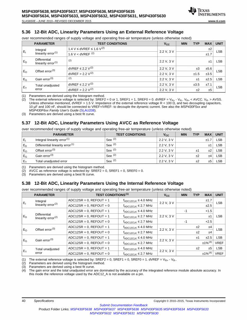
MSP430F5638, MSP430F5637, MSP430F5636, MSP430F5635MSP430F5634, MSP430F5633, MSP430F5632, MSP430F5631, MSP430F5630SLAS650E –JUNE 2010–REVISED DECEMBER 2015 www.ti.com
5.36 12-Bit ADC, Linearity Parameters Using an External Reference Voltageover recommended ranges of supply voltage and operating free-air temperature (unless otherwise noted)
PARAMETER TEST CONDITIONS VCC MIN TYP MAX UNIT1.4 V ≤ dVREF ≤ 1.6 V (2) ±2IntegralEI 2.2 V, 3 V LSBlinearity error (1) 1.6 V < dVREF (2) ±1.7
DifferentialED(2) 2.2 V, 3 V ±1 LSBlinearity error (1)
dVREF ≤ 2.2 V (2) 2.2 V, 3 V ±3 ±5.6EO Offset error (3) LSB
dVREF > 2.2 V (2) 2.2 V, 3 V ±1.5 ±3.5EG Gain error (3) (2) 2.2 V, 3 V ±1 ±2.5 LSB
dVREF ≤ 2.2 V (2) 2.2 V, 3 V ±3.5 ±7.1Total unadjustedET LSBerror dVREF > 2.2 V (2) 2.2 V, 3 V ±2 ±5
(1) Parameters are derived using the histogram method.(2) The external reference voltage is selected by: SREF2 = 0 or 1, SREF1 = 1, SREF0 = 0. dVREF = VR+ - VR-. VR+ < AVCC. VR- > AVSS.
Unless otherwise mentioned, dVREF > 1.5 V. Impedance of the external reference voltage R < 100 Ω, and two decoupling capacitors,10 µF and 100 nF, should be connected to VREF+/VREF- to decouple the dynamic current. See also the MSP430F5xx andMSP430F6xx Family User's Guide (SLAU208).
(3) Parameters are derived using a best fit curve.
5.37 12-Bit ADC, Linearity Parameters Using AVCC as Reference Voltageover recommended ranges of supply voltage and operating free-air temperature (unless otherwise noted)
PARAMETER TEST CONDITIONS VCC MIN TYP MAX UNITEI Integral linearity error (1) See (2) 2.2 V, 3 V ±1.7 LSBED Differential linearity error (1) See (2) 2.2 V, 3 V ±1 LSBEO Offset error (3) See (2) 2.2 V, 3 V ±1 ±2 LSBEG Gain error (3) See (2) 2.2 V, 3 V ±2 ±4 LSBET Total unadjusted error See (2) 2.2 V, 3 V ±2 ±5 LSB
(1) Parameters are derived using the histogram method.(2) AVCC as reference voltage is selected by: SREF2 = 0, SREF1 = 0, SREF0 = 0.(3) Parameters are derived using a best fit curve.
5.38 12-Bit ADC, Linearity Parameters Using the Internal Reference Voltageover recommended ranges of supply voltage and operating free-air temperature (unless otherwise noted)
PARAMETER TEST CONDITIONS (1) VCC MIN TYP MAX UNITADC12SR = 0, REFOUT = 1 fADC12CLK ≤ 4.0 MHz ±1.7IntegralEI 2.2 V, 3 V LSBlinearity error (2) ADC12SR = 0, REFOUT = 0 fADC12CLK ≤ 2.7 MHz ±2.5ADC12SR = 0, REFOUT = 1 fADC12CLK ≤ 4.0 MHz -1 +1.5
DifferentialED ADC12SR = 0, REFOUT = 1 fADC12CLK ≤ 2.7 MHz 2.2 V, 3 V ±1 LSBlinearity error (2)
ADC12SR = 0, REFOUT = 0 fADC12CLK ≤ 2.7 MHz -1 +2.5ADC12SR = 0, REFOUT = 1 fADC12CLK ≤ 4.0 MHz ±2 ±4
EO Offset error (3) 2.2 V, 3 V LSBADC12SR = 0, REFOUT = 0 fADC12CLK ≤ 2.7 MHz ±2 ±4ADC12SR = 0, REFOUT = 1 fADC12CLK ≤ 4.0 MHz ±1 ±2.5 LSB
EG Gain error (3) 2.2 V, 3 VADC12SR = 0, REFOUT = 0 fADC12CLK ≤ 2.7 MHz ±1% (4) VREFADC12SR = 0, REFOUT = 1 fADC12CLK ≤ 4.0 MHz ±2 ±5 LSBTotal unadjustedET 2.2 V, 3 Verror ADC12SR = 0, REFOUT = 0 fADC12CLK ≤ 2.7 MHz ±1% (4) VREF
(1) The external reference voltage is selected by: SREF2 = 0, SREF1 = 0, SREF0 = 1. dVREF = VR+ - VR-.(2) Parameters are derived using the histogram method.(3) Parameters are derived using a best fit curve.(4) The gain error and the total unadjusted error are dominated by the accuracy of the integrated reference module absolute accuracy. In
this mode the reference voltage used by the ADC12_A is not available on a pin.
40 Specifications Copyright © 2010–2015, Texas Instruments IncorporatedSubmit Documentation Feedback
Product Folder Links: MSP430F5638 MSP430F5637 MSP430F5636 MSP430F5635 MSP430F5634 MSP430F5633MSP430F5632 MSP430F5631 MSP430F5630
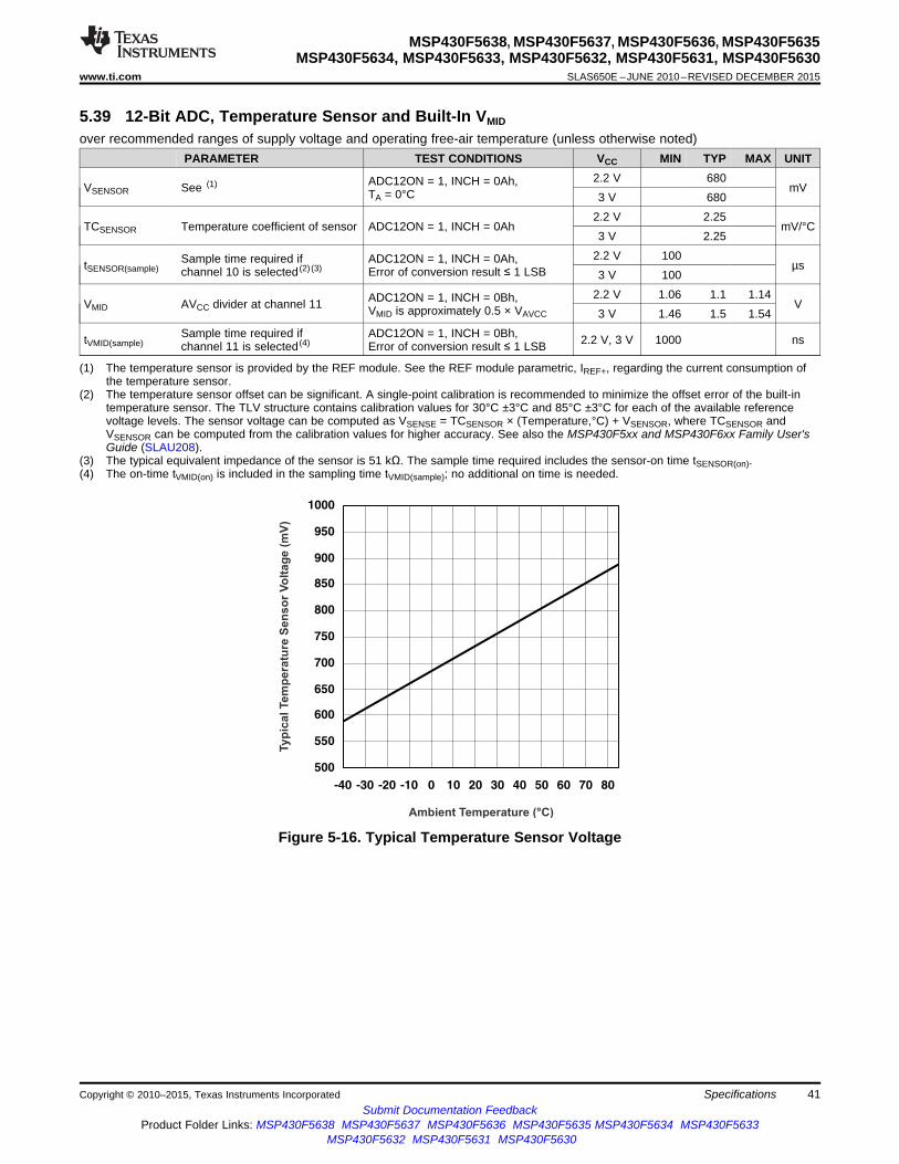
Ambient Temperature (°C)
500
550
600
650
700
750
800
850
900
950
1000
-40 -30 -20 -10 0 10 20 30 40 50 60 70 80
Typ
ical Tem
pera
ture
Sen
so
r V
olt
ag
e (
mV
)
MSP430F5638, MSP430F5637, MSP430F5636, MSP430F5635MSP430F5634, MSP430F5633, MSP430F5632, MSP430F5631, MSP430F5630
www.ti.com SLAS650E –JUNE 2010–REVISED DECEMBER 2015
5.39 12-Bit ADC, Temperature Sensor and Built-In VMID
over recommended ranges of supply voltage and operating free-air temperature (unless otherwise noted)PARAMETER TEST CONDITIONS VCC MIN TYP MAX UNIT
2.2 V 680ADC12ON = 1, INCH = 0Ah,VSENSOR See (1) mVTA = 0°C 3 V 6802.2 V 2.25
TCSENSOR Temperature coefficient of sensor ADC12ON = 1, INCH = 0Ah mV/°C3 V 2.25
2.2 V 100Sample time required if ADC12ON = 1, INCH = 0Ah,tSENSOR(sample) µschannel 10 is selected (2) (3) Error of conversion result ≤ 1 LSB 3 V 1002.2 V 1.06 1.1 1.14ADC12ON = 1, INCH = 0Bh,VMID AVCC divider at channel 11 VVMID is approximately 0.5 × VAVCC 3 V 1.46 1.5 1.54
Sample time required if ADC12ON = 1, INCH = 0Bh,tVMID(sample) 2.2 V, 3 V 1000 nschannel 11 is selected (4) Error of conversion result ≤ 1 LSB
(1) The temperature sensor is provided by the REF module. See the REF module parametric, IREF+, regarding the current consumption ofthe temperature sensor.
(2) The temperature sensor offset can be significant. A single-point calibration is recommended to minimize the offset error of the built-intemperature sensor. The TLV structure contains calibration values for 30°C ±3°C and 85°C ±3°C for each of the available referencevoltage levels. The sensor voltage can be computed as VSENSE = TCSENSOR × (Temperature,°C) + VSENSOR, where TCSENSOR andVSENSOR can be computed from the calibration values for higher accuracy. See also the MSP430F5xx and MSP430F6xx Family User'sGuide (SLAU208).
(3) The typical equivalent impedance of the sensor is 51 kΩ. The sample time required includes the sensor-on time tSENSOR(on).(4) The on-time tVMID(on) is included in the sampling time tVMID(sample); no additional on time is needed.
Figure 5-16. Typical Temperature Sensor Voltage
Copyright © 2010–2015, Texas Instruments Incorporated Specifications 41Submit Documentation Feedback
Product Folder Links: MSP430F5638 MSP430F5637 MSP430F5636 MSP430F5635 MSP430F5634 MSP430F5633MSP430F5632 MSP430F5631 MSP430F5630

MSP430F5638, MSP430F5637, MSP430F5636, MSP430F5635MSP430F5634, MSP430F5633, MSP430F5632, MSP430F5631, MSP430F5630SLAS650E –JUNE 2010–REVISED DECEMBER 2015 www.ti.com
5.40 REF, External Referenceover recommended ranges of supply voltage and operating free-air temperature (unless otherwise noted) (1)
PARAMETER TEST CONDITIONS VCC MIN TYP MAX UNITPositive externalVeREF+ VeREF+ > VREF-/VeREF-
(2) 1.4 AVCC Vreference voltage inputNegative externalVREF-/VeREF- VeREF+ > VREF-/VeREF-
(3) 0 1.2 Vreference voltage inputVeREF+ – Differential external VeREF+ > VREF-/VeREF-
(4) 1.4 AVCC VVREF-/VeREF- reference voltage input1.4 V ≤ VeREF+ ≤ VAVCC , VeREF- = 0 V,fADC12CLK = 5 MHz, ADC12SHTx = 1h, 2.2 V, 3 V –26 26Conversion rate 200 kspsIVeREF+, IVREF- Static input current µA
/VeREF- 1.4 V ≤ VeREF+ ≤ VAVCC , VeREF- = 0 V,fADC12CLK = 5 MHZ, ADC12SHTx = 8h, 2.2 V, 3 V –1.2 +1.2Conversion rate 20 ksps
Capacitance at VREF+CVREF+/- 10 µFor VREF- terminal (5)
(1) The external reference is used during ADC conversion to charge and discharge the capacitance array. The input capacitance, Ci, is alsothe dynamic load for an external reference during conversion. The dynamic impedance of the reference supply should follow therecommendations on analog-source impedance to let the charge settle for 12-bit accuracy.
(2) The accuracy limits the minimum positive external reference voltage. Lower reference voltage levels may be applied with reducedaccuracy requirements.
(3) The accuracy limits the maximum negative external reference voltage. Higher reference voltage levels may be applied with reducedaccuracy requirements.
(4) The accuracy limits minimum external differential reference voltage. Lower differential reference voltage levels may be applied withreduced accuracy requirements.
(5) Two decoupling capacitors, 10 µF and 100 nF, should be connected to VREF to decouple the dynamic current required for an externalreference source if it is used for the ADC12_A. See also the MSP430x5xx and MSP430x6xx Family User's Guide (SLAU208).
42 Specifications Copyright © 2010–2015, Texas Instruments IncorporatedSubmit Documentation Feedback
Product Folder Links: MSP430F5638 MSP430F5637 MSP430F5636 MSP430F5635 MSP430F5634 MSP430F5633MSP430F5632 MSP430F5631 MSP430F5630
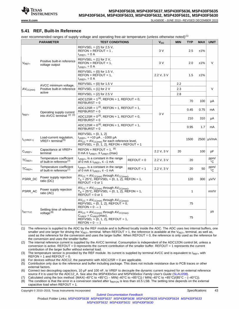
MSP430F5638, MSP430F5637, MSP430F5636, MSP430F5635MSP430F5634, MSP430F5633, MSP430F5632, MSP430F5631, MSP430F5630
www.ti.com SLAS650E –JUNE 2010–REVISED DECEMBER 2015
5.41 REF, Built-In Referenceover recommended ranges of supply voltage and operating free-air temperature (unless otherwise noted) (1)
PARAMETER TEST CONDITIONS VCC MIN TYP MAX UNITREFVSEL = 2 for 2.5 V,REFON = REFOUT = 1 , 3 V 2.5 ±1%IVREF+ = 0 AREFVSEL = 1 for 2 V,Positive built-in referenceVREF+ REFON = REFOUT = 1, 3 V 2.0 ±1% Vvoltage output IVREF+ = 0 AREFVSEL = 0 for 1.5 V,REFON = REFOUT = 1, 2.2 V, 3 V 1.5 ±1%IVREF+ = 0 AREFVSEL = 0 for 1.5 V 2.2AVCC minimum voltage,
AVCC(min) Positive built-in reference REFVSEL = 1 for 2 V 2.3 Vactive REFVSEL = 2 for 2.5 V 2.8
ADC12SR = 1 (4), REFON = 1, REFOUT = 0, 70 100 µAREFBURST = 0ADC12SR = 1 (4), REFON = 1, REFOUT = 1, 0.45 0.75 mAREFBURST = 0Operating supply currentIREF+ 3 Vinto AVCC terminal (2) (3) ADC12SR = 0 (4), REFON = 1, REFOUT = 0, 210 310 µAREFBURST = 0ADC12SR = 0 (4), REFON = 1, REFOUT = 1, 0.95 1.7 mAREFBURST = 0REFVSEL = 0, 1, 2
Load-current regulation, IVREF+ = +10 µA , –1000 µAIL(VREF+) 1500 2500 µV/mAVREF+ terminal (5) AVCC = AVCC(min) for each reference level,REFVSEL = 0, 1, 2, REFON = REFOUT = 1
Capacitance at VREF+ REFON = REFOUT = 1, (6)CVREF+ 2.2 V, 3 V 20 100 pFterminal 0 mA ≤ IVREF+ ≤ IVREF+(max)
Temperature coefficient IVREF+ is a constant in the range ppm/TCREF+ REFOUT = 0 2.2 V, 3 V 20of built-in reference (7) of 0 mA ≤ IVREF+ ≤ –1 mA °CTemperature coefficient IVREF+ is a constant in the range ppm/TCREF+ REFOUT = 1 2.2 V, 3 V 20 50of built-in reference (7) of 0 mA ≤ IVREF+ ≤ –1 mA °C
AVCC = AVCC(min) through AVCC(max),Power supply rejectionPSRR_DC TA = 25°C, REFVSEL = 0, 1, 2, REFON = 1, 120 300 µV/Vratio (DC) REFOUT = 0 or 1AVCC = AVCC(min) through AVCC(max),Power supply rejectionPSRR_AC TA = 25°C, REFVSEL = 0, 1, 2, REFON = 1, 1 mV/Vratio (AC) REFOUT = 0 or 1AVCC = AVCC(min) through AVCC(max),REFVSEL = 0, 1, 2, REFOUT = 0, 75REFON = 0 → 1
Settling time of referencetSETTLE µsAVCC = AVCC(min) through AVCC(max),voltage (8)CVREF = CVREF(max), 75REFVSEL = 0, 1, 2, REFOUT = 1,REFON = 0 → 1
(1) The reference is supplied to the ADC by the REF module and is buffered locally inside the ADC. The ADC uses two internal buffers, onesmaller and one larger for driving the VREF+ terminal. When REFOUT = 1, the reference is available at the VREF+ terminal, as well as,used as the reference for the conversion and uses the larger buffer. When REFOUT = 0, the reference is only used as the reference forthe conversion and uses the smaller buffer.
(2) The internal reference current is supplied by the AVCC terminal. Consumption is independent of the ADC12ON control bit, unless aconversion is active. REFOUT = 0 represents the current contribution of the smaller buffer. REFOUT = 1 represents the currentcontribution of the larger buffer without external load.
(3) The temperature sensor is provided by the REF module. Its current is supplied by terminal AVCC and is equivalent to IREF+ withREFON = 1 and REFOUT = 0.
(4) For devices without the ADC12, the parametric with ADC12SR = 0 are applicable.(5) Contribution only due to the reference and buffer including package. This does not include resistance due to PCB traces or other
external factors.(6) Connect two decoupling capacitors, 10 µF and 100 nF, to VREF to decouple the dynamic current required for an external reference
source if it is used for the ADC12_A. See also the MSP430x5xx and MSP430x6xx Family User's Guide (SLAU208).(7) Calculated using the box method: (MAX(–40°C to +85°C) – MIN(–40°C to +85°C)) / MIN(–40°C to +85°C)/(85°C – (–40°C)).(8) The condition is that the error in a conversion started after tREFON is less than ±0.5 LSB. The settling time depends on the external
capacitive load when REFOUT = 1.
Copyright © 2010–2015, Texas Instruments Incorporated Specifications 43Submit Documentation Feedback
Product Folder Links: MSP430F5638 MSP430F5637 MSP430F5636 MSP430F5635 MSP430F5634 MSP430F5633MSP430F5632 MSP430F5631 MSP430F5630

MSP430F5638, MSP430F5637, MSP430F5636, MSP430F5635MSP430F5634, MSP430F5633, MSP430F5632, MSP430F5631, MSP430F5630SLAS650E –JUNE 2010–REVISED DECEMBER 2015 www.ti.com
5.42 12-Bit DAC, Supply Specificationsover recommended ranges of supply voltage and operating free-air temperature (unless otherwise noted)
PARAMETER TEST CONDITIONS VCC MIN TYP MAX UNITAVCC Analog supply voltage AVCC = DVCC, AVSS = DVSS = 0 V 2.20 3.60 V
DAC12AMPx = 2, DAC12IR = 0,DAC12OG = 1, 3 V 65 110DAC12_xDAT = 0800h,VeREF+ = VREF+ = 1.5 VDAC12AMPx = 2, DAC12IR = 1,DAC12_xDAT = 0800h, 125 165VeREF+ = VREF+ = AVCCIDD Supply current, single DAC channel (1) (2) µADAC12AMPx = 5, DAC12IR = 1,DAC12_xDAT = 0800h, 2.2 V, 3 V 250 350VeREF+ = VREF+ = AVCC
DAC12AMPx = 7, DAC12IR = 1,DAC12_xDAT = 0800h, 750 1100VeREF+ = VREF+ = AVCC
DAC12_xDAT = 800h, 2.2 V 70VeREF+ = 1.5 V, ΔAVCC = 100 mVPSRR Power supply rejection ratio (3) (4) dBDAC12_xDAT = 800h,
VeREF+ = 1.5 V or 2.5 V, 3 V 70ΔAVCC = 100 mV
(1) No load at the output pin, DAC12_0 or DAC12_1, assuming that the control bits for the shared pins are set properly.(2) Current into reference terminals not included. If DAC12IR = 1 current flows through the input divider; see Reference Input specifications.(3) PSRR = 20 log (ΔAVCC / ΔVDAC12_xOUT)(4) The internal reference is not used.
5.43 12-Bit DAC, Linearity Specificationsover recommended ranges of supply voltage and operating free-air temperature (unless otherwise noted) (see Figure 5-17)
PARAMETER TEST CONDITIONS VCC MIN TYP MAX UNITResolution 12-bit monotonic 12 bits
VeREF+ = 1.5 V, DAC12AMPx = 7, DAC12IR = 1 2.2 V ±2 ±4 (2)IntegralINL LSBnonlinearity (1) VeREF+ = 2.5 V, DAC12AMPx = 7, DAC12IR = 1 3 V ±2 ±4VeREF+ = 1.5 V, DAC12AMPx = 7, DAC12IR = 1 2.2 V ±0.4 ±1 (2)DifferentialDNL LSBnonlinearity (1) VeREF+ = 2.5 V, DAC12AMPx = 7, DAC12IR = 1 3 V ±0.4 ±1
VeREF+ = 1.5 V,DAC12AMPx = 7, 2.2 V ±21 (2)
DAC12IR = 1Without calibration (1) (3)
VeREF+ = 2.5 V,DAC12AMPx = 7, 3 V ±21DAC12IR = 1
EO Offset voltage mVVeREF+ = 1.5 V,DAC12AMPx = 7, 2.2 V ±1.5 (2)
DAC12IR = 1With calibration (1) (3)
VeREF+ = 2.5 V,DAC12AMPx = 7, 3 V ±1.5DAC12IR = 1
Offset errordE(O)/dT temperature With calibration 2.2 V, 3 V ±10 µV/°C
coefficient (1)
VeREF+ = 1.5 V 2.2 V ±2.5EG Gain error %FSR
VeREF+ = 2.5 V 3 V ±2.5
(1) Parameters calculated from the best-fit curve from 0x0F to 0xFFF. The best-fit curve method is used to deliver coefficients "a" and "b" ofthe first-order equation: y = a + bx. VDAC12_xOUT = EO + (1 + EG) × (VeREF+ / 4095) × DAC12_xDAT, DAC12IR = 1.
(2) This parameter is not production tested.(3) The offset calibration works on the output operational amplifier. Offset calibration is triggered by setting the DAC12CALON bit.
44 Specifications Copyright © 2010–2015, Texas Instruments IncorporatedSubmit Documentation Feedback
Product Folder Links: MSP430F5638 MSP430F5637 MSP430F5636 MSP430F5635 MSP430F5634 MSP430F5633MSP430F5632 MSP430F5631 MSP430F5630

VR+
Gain ErrorOffset Error
DAC Code
DAC VOUT
Ideal transferfunction
R =Load ¥
AVCC
C = 100 pFLoad
2
DAC Output
Positive
Negative
MSP430F5638, MSP430F5637, MSP430F5636, MSP430F5635MSP430F5634, MSP430F5633, MSP430F5632, MSP430F5631, MSP430F5630
www.ti.com SLAS650E –JUNE 2010–REVISED DECEMBER 2015
12-Bit DAC, Linearity Specifications (continued)over recommended ranges of supply voltage and operating free-air temperature (unless otherwise noted) (see Figure 5-17)
PARAMETER TEST CONDITIONS VCC MIN TYP MAX UNITppm
Gain temperature ofdE(G)/dT 2.2 V, 3 V 10coefficient (1) FSR/°C
DAC12AMPx = 2 165Time for offsettOffset_Cal DAC12AMPx = 3, 5 2.2 V, 3 V 66 mscalibration (4)
DAC12AMPx = 4, 6, 7 16.5
(4) The offset calibration can be done if DAC12AMPx = 2, 3, 4, 5, 6, 7. The output operational amplifier is switched off with DAC12AMPx =0, 1. TI recommends configuring the DAC12 module before initiating calibration. Port activity during calibration may effect accuracyand is not recommended.
Figure 5-17. Linearity Test Load Conditions and Gain/Offset Definition
Copyright © 2010–2015, Texas Instruments Incorporated Specifications 45Submit Documentation Feedback
Product Folder Links: MSP430F5638 MSP430F5637 MSP430F5636 MSP430F5635 MSP430F5634 MSP430F5633MSP430F5632 MSP430F5631 MSP430F5630

RO/P(DAC12_x)
Max
0.3
AVCC
AV – 0.3 VCC VOUT
Min
RLoad
AVCC
C = 100 pFLoad
2
ILoad
DAC12
O/P(DAC12_x)
MSP430F5638, MSP430F5637, MSP430F5636, MSP430F5635MSP430F5634, MSP430F5633, MSP430F5632, MSP430F5631, MSP430F5630SLAS650E –JUNE 2010–REVISED DECEMBER 2015 www.ti.com
5.44 12-Bit DAC, Output Specificationsover recommended ranges of supply voltage and operating free-air temperature (unless otherwise noted)
PARAMETER TEST CONDITIONS VCC MIN TYP MAX UNITNo load, VeREF+ = AVCC,DAC12_xDAT = 0h, DAC12IR = 1, 0 0.005DAC12AMPx = 7No load, VeREF+ = AVCC, AVCC –DAC12_xDAT = 0FFFh, DAC12IR = 1, AVCC0.05Output voltage DAC12AMPx = 7
VO range (1) (see 2.2 V, 3 V VRLoad = 3 kΩ, VeREF+ = AVCC,Figure 5-18)DAC12_xDAT = 0h, DAC12IR = 1, 0 0.1DAC12AMPx = 7RLoad = 3 kΩ, VeREF+ = AVCC, AVCC –DAC12_xDAT = 0FFFh, DAC12IR = 1, AVCC0.13DAC12AMPx = 7
Maximum DAC12CL(DAC12) 2.2 V, 3 V 100 pFload capacitanceDAC12AMPx = 2, DAC12_xDAT = 0FFFh, –1VO/P(DAC12) > AVCC – 0.3Maximum DAC12IL(DAC12) 2.2 V, 3 V mAload current DAC12AMPx = 2, DAC12_xDAT = 0h, 1VO/P(DAC12) < 0.3 VRLoad = 3 kΩ, VO/P(DAC12) < 0.3 V, 150 250DAC12AMPx = 2, DAC12_xDAT = 0h
Output resistance RLoad = 3 kΩ, VO/P(DAC12) > AVCC – 0.3 V,RO/P(DAC12) 2.2 V, 3 V 150 250 Ω(see Figure 5-18) DAC12_xDAT = 0FFFhRLoad = 3 kΩ, 60.3 V ≤ VO/P(DAC12) ≤ AVCC – 0.3 V
(1) Data is valid after the offset calibration of the output amplifier.
Figure 5-18. DAC12_x Output Resistance Tests
46 Specifications Copyright © 2010–2015, Texas Instruments IncorporatedSubmit Documentation Feedback
Product Folder Links: MSP430F5638 MSP430F5637 MSP430F5636 MSP430F5635 MSP430F5634 MSP430F5633MSP430F5632 MSP430F5631 MSP430F5630

R = 3 kLoad W
AVCC
C = 100 pFLoad
2
DAC Output
RO/P(DAC12.x)
ILoad
Conversion 1 Conversion 2
VOUT
Conversion 3
GlitchEnergy
±1/2 LSB
±1/2 LSB
tsettleLH tsettleHL
MSP430F5638, MSP430F5637, MSP430F5636, MSP430F5635MSP430F5634, MSP430F5633, MSP430F5632, MSP430F5631, MSP430F5630
www.ti.com SLAS650E –JUNE 2010–REVISED DECEMBER 2015
5.45 12-Bit DAC, Reference Input Specificationsover recommended ranges of supply voltage and operating free-air temperature (unless otherwise noted)
PARAMETER TEST CONDITIONS VCC MIN TYP MAX UNITAVCC AVCCDAC12IR = 0 (1) (2)
/ 3 + 0.2Reference input voltageVeREF+ 2.2 V, 3 V Vrange AVCCDAC12IR = 1 (3) (4) AVCC + 0.2DAC12_0 IR = DAC12_1 IR = 0 20 MΩDAC12_0 IR = 1, DAC12_1 IR = 0 48
Ri(VREF+), Reference input resistance (5) 2.2 V, 3 VDAC12_0 IR = 0, DAC12_1 IR = 1 48Ri(VeREF+) kΩDAC12_0 IR = DAC12_1 IR = 1, 24DAC12_0 SREFx = DAC12_1 SREFx (6)
(1) For a full-scale output, the reference input voltage can be as high as 1/3 of the maximum output voltage swing (AVCC).(2) The maximum voltage applied at reference input voltage terminal VeREF+ = (AVCC – VE(O)) / (3 × (1 + EG)).(3) For a full-scale output, the reference input voltage can be as high as the maximum output voltage swing (AVCC).(4) The maximum voltage applied at reference input voltage terminal VeREF+ = (AVCC – VE(O)) / (1 + EG).(5) This impedance depends on tradeoff in power savings. Current devices have 48 kΩ for each channel when divide is enabled. Can be
increased if performance can be maintained.(6) When DAC12IR = 1 and DAC12SREFx = 0 or 1 for both channels, the reference input resistive dividers for each DAC are in parallel
reducing the reference input resistance.
5.46 12-Bit DAC, Dynamic SpecificationsVREF = VCC, DAC12IR = 1 (see Figure 5-19 and Figure 5-20), over recommended ranges of supply voltage and operating free-air temperature (unless otherwise noted)
PARAMETER TEST CONDITIONS VCC MIN TYP MAX UNITDAC12AMPx = 0 → 2, 3, 4 60 120DAC12_xDAT = 800h,
tON DAC12 on time ErrorV(O) < ±0.5 LSB (1) DAC12AMPx = 0 → 5, 6 2.2 V, 3 V 15 30 µs(see Figure 5-19) DAC12AMPx = 0 → 7 6 12
DAC12AMPx = 2 100 200DAC12_xDAT =tS(FS) Settling time, full scale DAC12AMPx = 3, 5 2.2 V, 3 V 40 80 µs80h → F7Fh → 80h
DAC12AMPx = 4, 6, 7 15 30DAC12AMPx = 2 5DAC12_xDAT =Settling time, code totS(C-C) 3F8h → 408h → 3F8h, DAC12AMPx = 3, 5 2.2 V, 3 V 2 µscode BF8h → C08h → BF8h DAC12AMPx = 4, 6, 7 1DAC12AMPx = 2 0.05 0.35
DAC12_xDAT =SR Slew rate DAC12AMPx = 3, 5 2.2 V, 3 V 0.35 1.10 V/µs80h → F7Fh → 80h (2)
DAC12AMPx = 4, 6, 7 1.50 5.20DAC12_xDAT =Glitch energy DAC12AMPx = 7 2.2 V, 3 V 35 nV-s800h → 7FFh → 800h
(1) RLoad and CLoad connected to AVSS (not AVCC/2) in Figure 5-19.(2) Slew rate applies to output voltage steps ≥ 200 mV.
Figure 5-19. Settling Time and Glitch Energy Testing
Copyright © 2010–2015, Texas Instruments Incorporated Specifications 47Submit Documentation Feedback
Product Folder Links: MSP430F5638 MSP430F5637 MSP430F5636 MSP430F5635 MSP430F5634 MSP430F5633MSP430F5632 MSP430F5631 MSP430F5630

DAC12_xDAT 080h
VOUT
1/fToggle
F7Fh
VDAC12_yOUT
080h F7Fh 080h
VDAC12_xOUT
RLoad
AVCC
C = 100 pFLoad
2
ILoad
DAC12_1
RLoad
AVCC
C = 100 pFLoad
2
ILoad
DAC12_0DAC0
DAC1
VREF+
VeREF+
AC
DC
R = 3 kLoad W
AVCC
C = 100 pFLoad
2
ILoad
DAC12_xDACx
Conversion 1 Conversion 2
VOUT
Conversion 3
10%
tSRLH
tSRHL
90%
10%
90%
MSP430F5638, MSP430F5637, MSP430F5636, MSP430F5635MSP430F5634, MSP430F5633, MSP430F5632, MSP430F5631, MSP430F5630SLAS650E –JUNE 2010–REVISED DECEMBER 2015 www.ti.com
Figure 5-20. Slew Rate Testing
5.47 12-Bit DAC, Dynamic Specifications (Continued)over recommended ranges of supply voltage and TA = 25°C (unless otherwise noted)
PARAMETER TEST CONDITIONS VCC MIN TYP MAX UNITDAC12AMPx = 2, 3, 4, DAC12SREFx = 2, 40DAC12IR = 1, DAC12_xDAT = 800h3-dB bandwidth,
VDC = 1.5 V, DAC12AMPx = 5, 6, DAC12SREFx = 2,BW–3dB 2.2 V, 3 V 180 kHzVAC = 0.1 VPP DAC12IR = 1, DAC12_xDAT = 800h(see Figure 5-21) DAC12AMPx = 7, DAC12SREFx = 2, 550DAC12IR = 1, DAC12_xDAT = 800h
DAC12_0DAT = 800h, No load,DAC12_1DAT = 80h ↔ F7Fh, RLoad = 3 kΩ, –80
Channel-to-channel fDAC12_1OUT = 10 kHz at 50/50 duty cyclecrosstalk (1) (see 2.2 V, 3 V dB
DAC12_0DAT = 80h ↔ F7Fh, RLoad = 3 kΩ,Figure 5-22)DAC12_1DAT = 800h, No load, –80fDAC12_0OUT = 10 kHz at 50/50 duty cycle
(1) RLoad = 3 kΩ, CLoad = 100 pF
Figure 5-21. Test Conditions for 3-dB Bandwidth Specification
Figure 5-22. Crosstalk Test Conditions
48 Specifications Copyright © 2010–2015, Texas Instruments IncorporatedSubmit Documentation Feedback
Product Folder Links: MSP430F5638 MSP430F5637 MSP430F5636 MSP430F5635 MSP430F5634 MSP430F5633MSP430F5632 MSP430F5631 MSP430F5630

MSP430F5638, MSP430F5637, MSP430F5636, MSP430F5635MSP430F5634, MSP430F5633, MSP430F5632, MSP430F5631, MSP430F5630
www.ti.com SLAS650E –JUNE 2010–REVISED DECEMBER 2015
5.48 Comparator_Bover recommended ranges of supply voltage and operating free-air temperature (unless otherwise noted)
PARAMETER TEST CONDITIONS VCC MIN TYP MAX UNITVCC Supply voltage 1.8 3.6 V
1.8 V 40Comparator operating CBPWRMD = 00 2.2 V 30 50supply current into AVCCIAVCC_COMP 3 V 40 65 µAterminal, Excludes
CBPWRMD = 01 2.2 V, 3 V 10 30reference resistor ladderCBPWRMD = 10 2.2 V, 3 V 0.1 0.5
Quiescent current of localIAVCC_REF reference voltage amplifier CBREFACC = 1, CBREFLx = 01 22 µA
into AVCC terminalCommon-mode inputVIC 0 VCC - 1 Vrange
CBPWRMD = 00 ±20VOFFSET Input offset voltage mV
CBPWRMD = 01, 10 ±10CIN Input capacitance 5 pF
ON (switch closed) 3 4 kΩRSIN Series input resistance
OFF (switch open) 50 MΩCBPWRMD = 00, CBF = 0 450
nsPropagation delay,tPD CBPWRMD = 01, CBF = 0 600response timeCBPWRMD = 10, CBF = 0 50 µsCBPWRMD = 00, CBON = 1, CBF = 1, 0.35 0.6 1.0CBFDLY = 00CBPWRMD = 00, CBON = 1, CBF = 1, 0.6 1.0 1.8CBFDLY = 01Propagation delay withtPD,filter µsfilter active CBPWRMD = 00, CBON = 1, CBF = 1, 1.0 1.8 3.4CBFDLY = 10CBPWRMD = 00, CBON = 1, CBF = 1, 1.8 3.4 6.5CBFDLY = 11
Comparator enable time, CBON = 0 to CBON = 1tEN_CMP 1 2 µssettling time CBPWRMD = 00, 01, 10Resistor reference enabletEN_REF CBON = 0 to CBON = 1 0.3 1.5 µstime
VIN × VIN × VIN ×Reference voltage for a VIN = reference into resistor ladder,VCB_REF (n + 0.5) (n + 1) (n + 1.5) Vgiven tap n = 0 to 31 / 32 / 32 / 32
Copyright © 2010–2015, Texas Instruments Incorporated Specifications 49Submit Documentation Feedback
Product Folder Links: MSP430F5638 MSP430F5637 MSP430F5636 MSP430F5635 MSP430F5634 MSP430F5633MSP430F5632 MSP430F5631 MSP430F5630
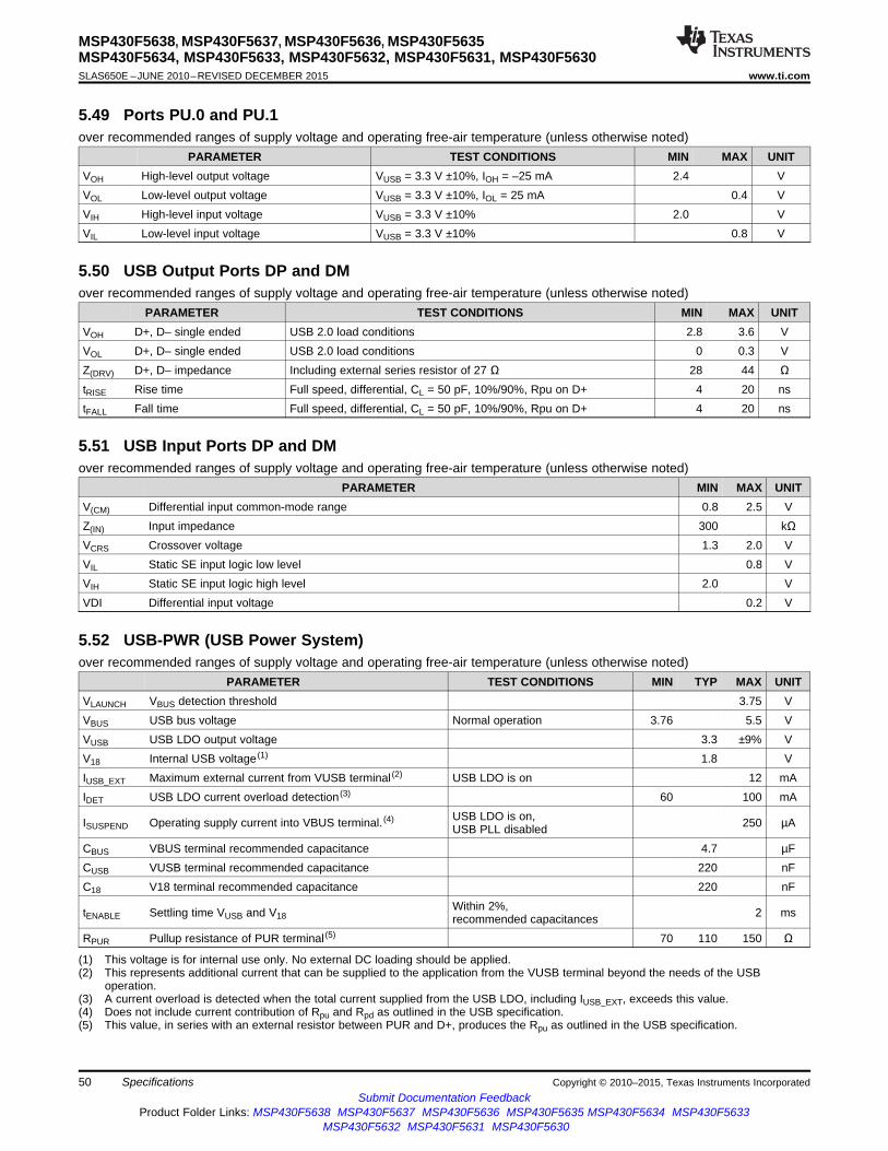
MSP430F5638, MSP430F5637, MSP430F5636, MSP430F5635MSP430F5634, MSP430F5633, MSP430F5632, MSP430F5631, MSP430F5630SLAS650E –JUNE 2010–REVISED DECEMBER 2015 www.ti.com
5.49 Ports PU.0 and PU.1over recommended ranges of supply voltage and operating free-air temperature (unless otherwise noted)
PARAMETER TEST CONDITIONS MIN MAX UNITVOH High-level output voltage VUSB = 3.3 V ±10%, IOH = –25 mA 2.4 VVOL Low-level output voltage VUSB = 3.3 V ±10%, IOL = 25 mA 0.4 VVIH High-level input voltage VUSB = 3.3 V ±10% 2.0 VVIL Low-level input voltage VUSB = 3.3 V ±10% 0.8 V
5.50 USB Output Ports DP and DMover recommended ranges of supply voltage and operating free-air temperature (unless otherwise noted)
PARAMETER TEST CONDITIONS MIN MAX UNITVOH D+, D– single ended USB 2.0 load conditions 2.8 3.6 VVOL D+, D– single ended USB 2.0 load conditions 0 0.3 VZ(DRV) D+, D– impedance Including external series resistor of 27 Ω 28 44 ΩtRISE Rise time Full speed, differential, CL = 50 pF, 10%/90%, Rpu on D+ 4 20 nstFALL Fall time Full speed, differential, CL = 50 pF, 10%/90%, Rpu on D+ 4 20 ns
5.51 USB Input Ports DP and DMover recommended ranges of supply voltage and operating free-air temperature (unless otherwise noted)
PARAMETER MIN MAX UNITV(CM) Differential input common-mode range 0.8 2.5 VZ(IN) Input impedance 300 kΩVCRS Crossover voltage 1.3 2.0 VVIL Static SE input logic low level 0.8 VVIH Static SE input logic high level 2.0 VVDI Differential input voltage 0.2 V
5.52 USB-PWR (USB Power System)over recommended ranges of supply voltage and operating free-air temperature (unless otherwise noted)
PARAMETER TEST CONDITIONS MIN TYP MAX UNITVLAUNCH VBUS detection threshold 3.75 VVBUS USB bus voltage Normal operation 3.76 5.5 VVUSB USB LDO output voltage 3.3 ±9% VV18 Internal USB voltage (1) 1.8 VIUSB_EXT Maximum external current from VUSB terminal (2) USB LDO is on 12 mAIDET USB LDO current overload detection (3) 60 100 mA
USB LDO is on,ISUSPEND Operating supply current into VBUS terminal. (4) 250 µAUSB PLL disabledCBUS VBUS terminal recommended capacitance 4.7 µFCUSB VUSB terminal recommended capacitance 220 nFC18 V18 terminal recommended capacitance 220 nF
Within 2%,tENABLE Settling time VUSB and V18 2 msrecommended capacitancesRPUR Pullup resistance of PUR terminal (5) 70 110 150 Ω
(1) This voltage is for internal use only. No external DC loading should be applied.(2) This represents additional current that can be supplied to the application from the VUSB terminal beyond the needs of the USB
operation.(3) A current overload is detected when the total current supplied from the USB LDO, including IUSB_EXT, exceeds this value.(4) Does not include current contribution of Rpu and Rpd as outlined in the USB specification.(5) This value, in series with an external resistor between PUR and D+, produces the Rpu as outlined in the USB specification.
50 Specifications Copyright © 2010–2015, Texas Instruments IncorporatedSubmit Documentation Feedback
Product Folder Links: MSP430F5638 MSP430F5637 MSP430F5636 MSP430F5635 MSP430F5634 MSP430F5633MSP430F5632 MSP430F5631 MSP430F5630

MSP430F5638, MSP430F5637, MSP430F5636, MSP430F5635MSP430F5634, MSP430F5633, MSP430F5632, MSP430F5631, MSP430F5630
www.ti.com SLAS650E –JUNE 2010–REVISED DECEMBER 2015
5.53 USB-PLL (USB Phase-Locked Loop)over recommended ranges of supply voltage and operating free-air temperature (unless otherwise noted)
PARAMETER TEST CONDITIONS VCC MIN TYP MAX UNITIPLL Operating supply current 7 mAfPLL PLL frequency 48 MHzfUPD PLL reference frequency 1.5 3 MHztLOCK PLL lock time 2 mstJitter PLL jitter 1000 ps
Copyright © 2010–2015, Texas Instruments Incorporated Specifications 51Submit Documentation Feedback
Product Folder Links: MSP430F5638 MSP430F5637 MSP430F5636 MSP430F5635 MSP430F5634 MSP430F5633MSP430F5632 MSP430F5631 MSP430F5630

MSP430F5638, MSP430F5637, MSP430F5636, MSP430F5635MSP430F5634, MSP430F5633, MSP430F5632, MSP430F5631, MSP430F5630SLAS650E –JUNE 2010–REVISED DECEMBER 2015 www.ti.com
5.54 Flash Memoryover recommended ranges of supply voltage and operating free-air temperature (unless otherwise noted)
PARAMETER TEST CONDITIONS MIN TYP MAX UNITDVCC(PGM/ERASE) Program and erase supply voltage 1.8 3.6 VIPGM Average supply current from DVCC during program 3 5 mAIERASE Average supply current from DVCC during erase 6 11 mA
Average supply current from DVCC during mass erase orIMERASE, IBANK 6 11 mAbank erasetCPT Cumulative program time See (1) 16 ms
Program and erase endurance 104 105 cyclestRetention Data retention duration TJ = 25°C 100 yearstWord Word or byte program time See (2) 64 85 µstBlock, 0 Block program time for first byte or word See (2) 49 65 µs
Block program time for each additional byte or word, excepttBlock, 1–(N–1) See (2) 37 49 µsfor last byte or wordtBlock, N Block program time for last byte or word See (2) 55 73 µs
Erase time for segment, mass erase, and bank erase whentSeg Erase See (2) 23 32 msavailableMCLK frequency in marginal read modefMCLK,MRG 0 1 MHz(FCTL4.MRG0 = 1 or FCTL4.MRG1 = 1)
(1) The cumulative program time must not be exceeded when writing to a 128-byte flash block. This parameter applies to all programmingmethods: individual word or byte write and block write modes.
(2) These values are hardwired into the flash controller state machine.
5.55 JTAG and Spy-Bi-Wire Interfaceover recommended ranges of supply voltage and operating free-air temperature (unless otherwise noted)
TESTPARAMETER MIN TYP MAX UNITCONDITIONSfSBW Spy-Bi-Wire input frequency 2.2 V, 3 V 0 20 MHztSBW,Low Spy-Bi-Wire low clock pulse duration 2.2 V, 3 V 0.025 15 µstSBW, En Spy-Bi-Wire enable time (TEST high to acceptance of first clock edge) (1) 2.2 V, 3 V 1 µstSBW,Rst Spy-Bi-Wire return to normal operation time 15 100 µs
2.2 V 0 5 MHzfTCK TCK input frequency (4-wire JTAG) (2)
3 V 0 10 MHzRinternal Internal pulldown resistance on TEST 2.2 V, 3 V 45 60 80 kΩ
(1) Tools that access the Spy-Bi-Wire interface must wait for the tSBW,En time after pulling the TEST/SBWTCK pin high before applying thefirst SBWTCK clock edge.
(2) fTCK may be restricted to meet the timing requirements of the module selected.
52 Specifications Copyright © 2010–2015, Texas Instruments IncorporatedSubmit Documentation Feedback
Product Folder Links: MSP430F5638 MSP430F5637 MSP430F5636 MSP430F5635 MSP430F5634 MSP430F5633MSP430F5632 MSP430F5631 MSP430F5630

Program Counter PC/R0
Stack Pointer SP/R1
Status Register SR/CG1/R2
Constant Generator CG2/R3
General-Purpose Register R4
General-Purpose Register R5
General-Purpose Register R6
General-Purpose Register R7
General-Purpose Register R8
General-Purpose Register R9
General-Purpose Register R10
General-Purpose Register R11
General-Purpose Register R12
General-Purpose Register R13
General-Purpose Register R15
General-Purpose Register R14
MSP430F5638, MSP430F5637, MSP430F5636, MSP430F5635MSP430F5634, MSP430F5633, MSP430F5632, MSP430F5631, MSP430F5630
www.ti.com SLAS650E –JUNE 2010–REVISED DECEMBER 2015
6 Detailed Description
6.1 OverviewThe MSP430F563x devices include a high-performance 12-bit ADC, a comparator, two USCIs, USB 2.0, ahardware multiplier, DMA, four 16-bit timers, an RTC module with alarm capabilities, and up to 74 I/O pins.
6.2 CPUThe MSP430 CPU has a 16-bit RISC architecture that is highly transparent to the application. Alloperations, other than program-flow instructions, are performed as register operations in conjunction withseven addressing modes for source operand and four addressing modes for destination operand.
The CPU is integrated with 16 registers that provide reduced instruction execution time. The register-to-register operation execution time is one cycle of the CPU clock.
Four of the registers, R0 to R3, are dedicated as program counter, stack pointer, status register, andconstant generator, respectively. The remaining registers are general-purpose registers (see Figure 6-1).
Peripherals are connected to the CPU using data, address, and control buses. Peripherals can bemanaged with all instructions.
Figure 6-1. CPU Registers
Copyright © 2010–2015, Texas Instruments Incorporated Detailed Description 53Submit Documentation Feedback
Product Folder Links: MSP430F5638 MSP430F5637 MSP430F5636 MSP430F5635 MSP430F5634 MSP430F5633MSP430F5632 MSP430F5631 MSP430F5630

MSP430F5638, MSP430F5637, MSP430F5636, MSP430F5635MSP430F5634, MSP430F5633, MSP430F5632, MSP430F5631, MSP430F5630SLAS650E –JUNE 2010–REVISED DECEMBER 2015 www.ti.com
6.3 Instruction SetThe instruction set consists of the original 51 instructions with three formats and seven address modesand additional instructions for the expanded address range. Each instruction can operate on word andbyte data. Table 6-1 shows examples of the three types of instruction formats; Table 6-2 shows theaddress modes.
Table 6-1. Instruction Word Formats
INSTRUCTION WORD FORMAT EXAMPLE OPERATIONDual operands, source-destination ADD R4,R5 R4 + R5 → R5Single operands, destination only CALL R8 PC → (TOS), R8 → PCRelative jump, un/conditional JNE Jump-on-equal bit = 0
Table 6-2. Address Mode Descriptions
ADDRESS MODE S (1) D (1) SYNTAX EXAMPLE OPERATIONRegister + + MOV Rs,Rd MOV R10,R11 R10 → R11Indexed + + MOV X(Rn),Y(Rm) MOV 2(R5),6(R6) M(2+R5) → M(6+R6)
Symbolic (PC relative) + + MOV EDE,TONI M(EDE) → M(TONI)Absolute + + MOV &MEM, &TCDAT M(MEM) → M(TCDAT)Indirect + MOV @Rn,Y(Rm) MOV @R10,Tab(R6) M(R10) → M(Tab+R6)
M(R10) → R11Indirect auto-increment + MOV @Rn+,Rm MOV @R10+,R11 R10 + 2 → R10Immediate + MOV #X,TONI MOV #45,TONI #45 → M(TONI)
(1) S = source, D = destination
54 Detailed Description Copyright © 2010–2015, Texas Instruments IncorporatedSubmit Documentation Feedback
Product Folder Links: MSP430F5638 MSP430F5637 MSP430F5636 MSP430F5635 MSP430F5634 MSP430F5633MSP430F5632 MSP430F5631 MSP430F5630
MSP430F5638, MSP430F5637, MSP430F5636, MSP430F5635MSP430F5634, MSP430F5633, MSP430F5632, MSP430F5631, MSP430F5630
www.ti.com SLAS650E –JUNE 2010–REVISED DECEMBER 2015
6.4 Operating ModesThese devices have one active mode and seven software-selectable low-power modes of operation. Aninterrupt event can wake up the device from any of the low-power modes, service the request, and restoreback to the low-power mode on return from the interrupt program.
Software can configure the following operating modes:• Active mode (AM)
– All clocks are active• Low-power mode 0 (LPM0)
– CPU is disabled– ACLK and SMCLK remain active, MCLK is disabled– FLL loop control remains active
• Low-power mode 1 (LPM1)– CPU is disabled– FLL loop control is disabled– ACLK and SMCLK remain active, MCLK is disabled
• Low-power mode 2 (LPM2)– CPU is disabled– MCLK, FLL loop control, and DCOCLK are disabled– DC generator of the DCO remains enabled– ACLK remains active
• Low-power mode 3 (LPM3)– CPU is disabled– MCLK, FLL loop control, and DCOCLK are disabled– DC generator of the DCO is disabled– ACLK remains active
• Low-power mode 4 (LPM4)– CPU is disabled– ACLK is disabled– MCLK, FLL loop control, and DCOCLK are disabled– DC generator of the DCO is disabled– Crystal oscillator is stopped– Complete data retention
• Low-power mode 3.5 (LPM3.5)– Internal regulator disabled– No data retention– RTC enabled and clocked by low-frequency oscillator– Wake-up signal from RST/NMI, RTC_B, P1, P2, P3, and P4
• Low-power mode 4.5 (LPM4.5)– Internal regulator disabled– No data retention– Wake-up signal from RST/NMI, P1, P2, P3, and P4
Copyright © 2010–2015, Texas Instruments Incorporated Detailed Description 55Submit Documentation Feedback
Product Folder Links: MSP430F5638 MSP430F5637 MSP430F5636 MSP430F5635 MSP430F5634 MSP430F5633MSP430F5632 MSP430F5631 MSP430F5630

MSP430F5638, MSP430F5637, MSP430F5636, MSP430F5635MSP430F5634, MSP430F5633, MSP430F5632, MSP430F5631, MSP430F5630SLAS650E –JUNE 2010–REVISED DECEMBER 2015 www.ti.com
6.5 Interrupt Vector AddressesThe interrupt vectors and the power-up start address are located in the address range 0FFFFh to 0FF80h.The vector contains the 16-bit address of the appropriate interrupt-handler instruction sequence (seeTable 6-3).
Table 6-3. Interrupt Sources, Flags, and Vectors of MSP430F563x Configurations
SYSTEM WORDINTERRUPT SOURCE INTERRUPT FLAG PRIORITYINTERRUPT ADDRESSSystem Reset
Power-Up, External Reset WDTIFG, KEYV (SYSRSTIV) (1) (2) Reset 0FFFEh 63, highestWatchdog Time-out, Key ViolationFlash Memory Key Violation
System NMI SVMLIFG, SVMHIFG, DLYLIFG, DLYHIFG,PMM VLRLIFG, VLRHIFG, VMAIFG, JMBNIFG, (Non)maskable 0FFFCh 62Vacant Memory Access JMBOUTIFG (SYSSNIV) (1)JTAG Mailbox
User NMINMI NMIIFG, OFIFG, ACCVIFG, BUSIFG (Non)maskable 0FFFAh 61Oscillator Fault (SYSUNIV) (1) (2)
Flash Memory Access ViolationComp_B Comparator B interrupt flags (CBIV) (1) (3) Maskable 0FFF8h 60
Timer TB0 TB0CCR0 CCIFG0 (3) Maskable 0FFF6h 59TB0CCR1 CCIFG1 to TB0CCR6 CCIFG6,Timer TB0 Maskable 0FFF4h 58TB0IFG (TBIV) (1) (3)
Watchdog Interval Timer Mode WDTIFG Maskable 0FFF2h 57USCI_A0 Receive or Transmit UCA0RXIFG, UCA0TXIFG (UCA0IV) (1) (3) Maskable 0FFF0h 56USCI_B0 Receive or Transmit UCB0RXIFG, UCB0TXIFG (UCB0IV) (1) (3) Maskable 0FFEEh 55
ADC12_A (4) ADC12IFG0 to ADC12IFG15 (ADC12IV) (1) (3) Maskable 0FFECh 54Timer TA0 TA0CCR0 CCIFG0 (3) Maskable 0FFEAh 53
TA0CCR1 CCIFG1 to TA0CCR4 CCIFG4,Timer TA0 Maskable 0FFE8h 52TA0IFG (TA0IV) (1) (3)
USB_UBM USB interrupts (USBIV) (1) (3) Maskable 0FFE6h 51DMA0IFG, DMA1IFG, DMA2IFG, DMA3IFG,DMA Maskable 0FFE4h 50DMA4IFG, DMA5IFG (DMAIV) (1) (3)
Timer TA1 TA1CCR0 CCIFG0 (3) Maskable 0FFE2h 49TA1CCR1 CCIFG1 to TA1CCR2 CCIFG2,Timer TA1 Maskable 0FFE0h 48TA1IFG (TA1IV) (1) (3)
I/O Port P1 P1IFG.0 to P1IFG.7 (P1IV) (1) (3) Maskable 0FFDEh 47USCI_A1 Receive or Transmit UCA1RXIFG, UCA1TXIFG (UCA1IV) (1) (3) Maskable 0FFDCh 46USCI_B1 Receive or Transmit UCB1RXIFG, UCB1TXIFG (UCB1IV) (1) (3) Maskable 0FFDAh 45
I/O Port P2 P2IFG.0 to P2IFG.7 (P2IV) (1) (3) Maskable 0FFD8h 44Reserved Reserved Maskable 0FFD6h 43
RTCRDYIFG, RTCTEVIFG, RTCAIFG,RTC_B Maskable 0FFD4h 42RT0PSIFG, RT1PSIFG, RTCOFIFG (RTCIV) (1) (3)
DAC12_A (5) DAC12_0IFG, DAC12_1IFG (1) (3) Maskable 0FFD2h 41Timer TA2 TA2CCR0 CCIFG0 (3) Maskable 0FFD0h 40
TA2CCR1 CCIFG1 to TA2CCR2 CCIFG2,Timer TA2 Maskable 0FFCEh 39TA2IFG (TA2IV) (1) (3)
I/O Port P3 P3IFG.0 to P3IFG.7 (P3IV) (1) (3) Maskable 0FFCCh 38I/O Port P4 P4IFG.0 to P4IFG.7 (P4IV) (1) (3) Maskable 0FFCAh 37
(1) Multiple source flags(2) A reset is generated if the CPU tries to fetch instructions from within peripheral space or vacant memory space.
(Non)maskable: the individual interrupt-enable bit can disable an interrupt event, but the general-interrupt enable cannot disable it.(3) Interrupt flags are located in the module.(4) Only on devices with peripheral module ADC12_A, otherwise reserved.(5) Only on devices with peripheral module DAC12_A, otherwise reserved.
56 Detailed Description Copyright © 2010–2015, Texas Instruments IncorporatedSubmit Documentation Feedback
Product Folder Links: MSP430F5638 MSP430F5637 MSP430F5636 MSP430F5635 MSP430F5634 MSP430F5633MSP430F5632 MSP430F5631 MSP430F5630

MSP430F5638, MSP430F5637, MSP430F5636, MSP430F5635MSP430F5634, MSP430F5633, MSP430F5632, MSP430F5631, MSP430F5630
www.ti.com SLAS650E –JUNE 2010–REVISED DECEMBER 2015
Table 6-3. Interrupt Sources, Flags, and Vectors of MSP430F563x Configurations (continued)SYSTEM WORDINTERRUPT SOURCE INTERRUPT FLAG PRIORITYINTERRUPT ADDRESS
0FFC8h 36Reserved Reserved (6) ⋮ ⋮
0FF80h 0, lowest
(6) Reserved interrupt vectors at addresses are not used in this device and can be used for regular program code if necessary. To maintaincompatibility with other devices, TI recommends reserving these locations.
6.6 MemoryTable 6-4 shows the memory organization for all device variants.
Table 6-4. Memory Organization (1) (2)
MSP430F5636 MSP430F5637 MSP430F5638MSP430F5633 MSP430F5634 MSP430F5635MSP430F5630 MSP430F5631 MSP430F5632
Memory (flash) Total Size 128KB 192KB 256KBMain: interrupt vector 00FFFFh-00FF80h 00FFFFh-00FF80h 00FFFFh-00FF80h
Bank 3 N/A N/A 64KB047FFFh-038000h
Bank 2 N/A 64KB 64KB037FFFh-028000h 037FFFh-028000h
Main: code memoryBank 1 64KB 64KB 64KB
027FFFh-018000h 027FFFh-018000h 027FFFh-018000hBank 0 64KB 64KB 64KB
017FFFh-008000h 017FFFh-008000h 017FFFh-008000hSector 3 4KB 4KB 4KB
0063FFh-005400h 0063FFh-005400h 0063FFh-005400hSector 2 4KB 4KB 4KB
0053FFh-004400h 0053FFh-004400h 0053FFh-004400hRAM
Sector 1 4KB 4KB 4KB0043FFh-003400h 0043FFh-003400h 0043FFh-003400h
Sector 0 4KB 4KB 4KB0033FFh-002400h 0033FFh-002400h 0033FFh-002400h
Size 2KB 2KB 2KBUSB RAM (3)RAM 0023FFh-001C00h 0023FFh-001C00h 0023FFh-001C00h
Info A 128 B 128 B 128 B0019FFh-001980h 0019FFh-001980h 0019FFh-001980h
Info B 128 B 128 B 128 B00197Fh-001900h 00197Fh-001900h 00197Fh-001900hInformation memory
(flash) Info C 128 B 128 B 128 B0018FFh-001880h 0018FFh-001880h 0018FFh-001880h
Info D 128 B 128 B 128 B00187Fh-001800h 00187Fh-001800h 00187Fh-001800h
BSL 3 512 B 512 B 512 B0017FFh-001600h 0017FFh-001600h 0017FFh-001600h
BSL 2 512 B 512 B 512 B0015FFh-001400h 0015FFh-001400h 0015FFh-001400hBootloader (BSL)
memory (flash) BSL 1 512 B 512 B 512 B0013FFh-001200h 0013FFh-001200h 0013FFh-001200h
BSL 0 512 B 512 B 512 B0011FFh-001000h 0011FFh-001000h 0011FFh-001000h
Size 4KB 4KB 4KBPeripherals 000FFFh-000000h 000FFFh-000000h 000FFFh-000000h
(1) N/A = Not available.(2) Backup RAM is accessed through the control registers BAKMEM0, BAKMEM1, BAKMEM2, and BAKMEM3.(3) USB RAM can be used as general-purpose RAM when not used for USB operation.
Copyright © 2010–2015, Texas Instruments Incorporated Detailed Description 57Submit Documentation Feedback
Product Folder Links: MSP430F5638 MSP430F5637 MSP430F5636 MSP430F5635 MSP430F5634 MSP430F5633MSP430F5632 MSP430F5631 MSP430F5630

MSP430F5638, MSP430F5637, MSP430F5636, MSP430F5635MSP430F5634, MSP430F5633, MSP430F5632, MSP430F5631, MSP430F5630SLAS650E –JUNE 2010–REVISED DECEMBER 2015 www.ti.com
6.7 Bootloader (BSL)The BSL enables users to program the flash memory or RAM using various serial interfaces. Access tothe device memory by the BSL is protected by an user-defined password. For complete description of thefeatures of the BSL and its implementation, see MSP430 Programming With the Bootloader (BSL)(SLAU319).
6.7.1 USB BSLAll devices come preprogrammed with the USB BSL. Use of the USB BSL requires external access to sixpins (see Table 6-5). In addition to these pins, the application must support external componentsnecessary for normal USB operation; for example, the proper crystal on XT2IN and XT2OUT or properdecoupling.
Table 6-5. USB BSL Pin Requirements and Functions
DEVICE SIGNAL BSL FUNCTIONRST/NMI/SBWTDIO Entry sequence signal
PU.0/DP USB data terminal DPPU.1/DM USB data terminal DM
PUR USB pullup resistor terminalVBUS USB bus power supplyVSSU USB ground supply
NOTEThe default USB BSL evaluates the logic level of the PUR pin after a BOR reset. If the PURpin is pulled high externally, the BSL is invoked. Therefore, unless the application is invokingthe BSL, it is important to keep PUR pulled low after a BOR reset, even if BSL or USB isnever used. TI recommends applying a 1-MΩ resistor to ground.
6.7.2 UART BSLA UART BSL is also available that can be programmed by the user into the BSL memory by replacing thepreprogrammed, factory supplied, USB BSL. Use of the UART BSL requires external access to six pins(see Table 6-6).
Table 6-6. UART BSL Pin Requirements and Functions
DEVICE SIGNAL BSL FUNCTIONRST/NMI/SBWTDIO Entry sequence signal
TEST/SBWTCK Entry sequence signalP1.1 Data transmitP1.2 Data receiveVCC Power supplyVSS Ground supply
58 Detailed Description Copyright © 2010–2015, Texas Instruments IncorporatedSubmit Documentation Feedback
Product Folder Links: MSP430F5638 MSP430F5637 MSP430F5636 MSP430F5635 MSP430F5634 MSP430F5633MSP430F5632 MSP430F5631 MSP430F5630

MSP430F5638, MSP430F5637, MSP430F5636, MSP430F5635MSP430F5634, MSP430F5633, MSP430F5632, MSP430F5631, MSP430F5630
www.ti.com SLAS650E –JUNE 2010–REVISED DECEMBER 2015
6.8 JTAG Operation
6.8.1 JTAG Standard InterfaceThe MSP430 family supports the standard JTAG interface which requires four signals for sending andreceiving data. The JTAG signals are shared with general-purpose I/O. The TEST/SBWTCK pin is used toenable the JTAG signals. In addition to these signals, the RST/NMI/SBWTDIO is required to interface withMSP430 development tools and device programmers. Table 6-7 lists the JTAG pin requirements. Forfurther details on interfacing to development tools and device programmers, see the MSP430™ HardwareTools User's Guide (SLAU278). For a complete description of the features of the JTAG interface and itsimplementation, see MSP430 Programming Via the JTAG Interface (SLAU320).
Table 6-7. JTAG Pin Requirements and Functions
DEVICE SIGNAL DIRECTION FUNCTIONPJ.3/TCK IN JTAG clock inputPJ.2/TMS IN JTAG state control
PJ.1/TDI/TCLK IN JTAG data input, TCLK inputPJ.0/TDO OUT JTAG data output
TEST/SBWTCK IN Enable JTAG pinsRST/NMI/SBWTDIO IN External reset
VCC Power supplyVSS Ground supply
6.8.2 Spy-Bi-Wire InterfaceIn addition to the standard JTAG interface, the MSP430 family supports the two wire Spy-Bi-Wireinterface. Spy-Bi-Wire can be used to interface with MSP430 development tools and device programmers.Table 6-8 lists the Spy-Bi-Wire interface pin requirements. For further details on interfacing todevelopment tools and device programmers, see the MSP430 Hardware Tools User's Guide (SLAU278).For a complete description of the features of the JTAG interface and its implementation, see MSP430Programming Via the JTAG Interface (SLAU320).
Table 6-8. Spy-Bi-Wire Pin Requirements and Functions
DEVICE SIGNAL DIRECTION FUNCTIONTEST/SBWTCK IN Spy-Bi-Wire clock input
RST/NMI/SBWTDIO IN, OUT Spy-Bi-Wire data input/outputVCC Power supplyVSS Ground supply
6.9 Flash Memory (Link to User's Guide)The flash memory can be programmed by the JTAG port, Spy-Bi-Wire (SBW), the BSL, or in-system bythe CPU. The CPU can perform single-byte, single-word, and long-word writes to the flash memory.Features of the flash memory include:• Flash memory has n segments of main memory and four segments of information memory (A to D) of
128 bytes each. Each segment in main memory is 512 bytes in size.• Segments 0 to n may be erased in one step, or each segment may be individually erased.• Segments A to D can be erased individually, or as a group with segments 0 to n. Segments A to D are
also called information memory.• Segment A can be locked separately.
Copyright © 2010–2015, Texas Instruments Incorporated Detailed Description 59Submit Documentation Feedback
Product Folder Links: MSP430F5638 MSP430F5637 MSP430F5636 MSP430F5635 MSP430F5634 MSP430F5633MSP430F5632 MSP430F5631 MSP430F5630

MSP430F5638, MSP430F5637, MSP430F5636, MSP430F5635MSP430F5634, MSP430F5633, MSP430F5632, MSP430F5631, MSP430F5630SLAS650E –JUNE 2010–REVISED DECEMBER 2015 www.ti.com
6.10 RAM (Link to User's Guide)The RAM is made up of n sectors. Each sector can be completely powered down to save leakage;however, all data is lost. Features of the RAM include:• RAM has n sectors. The size of a sector can be found in Memory Organization.• Each sector 0 to n can be complete disabled; however, data retention is lost.• Each sector 0 to n automatically enters low power retention mode when possible.• For devices that contain USB memory, the USB memory can be used as normal RAM if USB is not
required.
6.11 Backup RAMThe backup RAM provides a limited number of bytes of RAM that are retained during LPMx.5 and duringoperation from a backup supply if the Battery Backup System module is implemented.
There are 8 bytes of backup RAM available on MSP430F563x. It can be wordwise accessed by thecontrol registers BAKMEM0, BAKMEM1, BAKMEM2, and BAKMEM3.
6.12 PeripheralsPeripherals are connected to the CPU through data, address, and control buses and can be handled usingall instructions. For complete module descriptions, see the MSP430x5xx and MSP430x6xx Family User'sGuide (SLAU208).
6.12.1 Digital I/O (Link to User's Guide)Up to nine 8-bit I/O ports are implemented: P1 through P6, P8, and P9 are complete, P7 contains sixindividual I/O ports, and PJ contains four individual I/O ports.• All individual I/O bits are independently programmable.• Any combination of input, output, and interrupt conditions is possible.• Programmable pullup or pulldown on all ports.• Programmable drive strength on all ports.• Edge-selectable interrupt input capability for all the eight bits of ports P1, P2, P3, and P4.• Read and write access to port-control registers is supported by all instructions.• Ports can be accessed byte-wise (P1 through P9) or word-wise in pairs (PA through PD).
6.12.2 Port Mapping Controller (Link to User's Guide)The port mapping controller allows the flexible and reconfigurable mapping of digital functions to port P2.Table 6-9 lists the mnemonic for each function that can be assigned.
Table 6-9. Port Mapping Mnemonics and Functions
VALUE PxMAPy MNEMONIC INPUT PIN FUNCTION OUTPUT PIN FUNCTION0 PM_NONE None DVSS
PM_CBOUT - Comparator_B output1
PM_TB0CLK Timer TB0 clock input -PM_ADC12CLK - ADC12CLK
2PM_DMAE0 DMAE0 Input -
PM_SVMOUT - SVM output3 Timer TB0 high impedance inputPM_TB0OUTH -TB0OUTH4 PM_TB0CCR0B Timer TB0 CCR0 capture input CCI0B Timer TB0: TB0.0 compare output Out05 PM_TB0CCR1B Timer TB0 CCR1 capture input CCI1B Timer TB0: TB0.1 compare output Out16 PM_TB0CCR2B Timer TB0 CCR2 capture input CCI2B Timer TB0: TB0.2 compare output Out2
60 Detailed Description Copyright © 2010–2015, Texas Instruments IncorporatedSubmit Documentation Feedback
Product Folder Links: MSP430F5638 MSP430F5637 MSP430F5636 MSP430F5635 MSP430F5634 MSP430F5633MSP430F5632 MSP430F5631 MSP430F5630

MSP430F5638, MSP430F5637, MSP430F5636, MSP430F5635MSP430F5634, MSP430F5633, MSP430F5632, MSP430F5631, MSP430F5630
www.ti.com SLAS650E –JUNE 2010–REVISED DECEMBER 2015
Table 6-9. Port Mapping Mnemonics and Functions (continued)VALUE PxMAPy MNEMONIC INPUT PIN FUNCTION OUTPUT PIN FUNCTION
7 PM_TB0CCR3B Timer TB0 CCR3 capture input CCI3B Timer TB0: TB0.3 compare output Out38 PM_TB0CCR4B Timer TB0 CCR4 capture input CCI4B Timer TB0: TB0.4 compare output Out49 PM_TB0CCR5B Timer TB0 CCR5 capture input CCI5B Timer TB0: TB0.5 compare output Out5
10 PM_TB0CCR6B Timer TB0 CCR6 capture input CCI6B Timer TB0: TB0.6 compare output Out6PM_UCA0RXD USCI_A0 UART RXD (Direction controlled by USCI – input)
11PM_UCA0SOMI USCI_A0 SPI slave out master in (direction controlled by USCI)PM_UCA0TXD USCI_A0 UART TXD (Direction controlled by USCI – output)
12PM_UCA0SIMO USCI_A0 SPI slave in master out (direction controlled by USCI)PM_UCA0CLK USCI_A0 clock input/output (direction controlled by USCI)
13PM_UCB0STE USCI_B0 SPI slave transmit enable (direction controlled by USCI – input)
PM_UCB0SOMI USCI_B0 SPI slave out master in (direction controlled by USCI)14
PM_UCB0SCL USCI_B0 I2C clock (open drain and direction controlled by USCI)PM_UCB0SIMO USCI_B0 SPI slave in master out (direction controlled by USCI)
15PM_UCB0SDA USCI_B0 I2C data (open drain and direction controlled by USCI)PM_UCB0CLK USCI_B0 clock input/output (direction controlled by USCI)
16PM_UCA0STE USCI_A0 SPI slave transmit enable (direction controlled by USCI – input)
17 PM_MCLK - MCLK18 Reserved Reserved for test purposes. Do not use this setting.19 Reserved Reserved for test purposes. Do not use this setting.
20-30 Reserved None DVSSDisables the output driver and the input Schmitt-trigger to prevent parasitic cross currents31 (0FFh) (1) PM_ANALOG when applying analog signals.
(1) The value of the PM_ANALOG mnemonic is set to 0FFh. The port mapping registers are 5 bits wide and the upper bits are ignored,which results in a maximum value of 31.
Table 6-10 lists the default port mapping for all supported pins.
Table 6-10. Default Mapping
PxMAPyPIN INPUT PIN FUNCTION OUTPUT PIN FUNCTIONMNEMONICPM_UCB0STE, USCI_B0 SPI slave transmit enable (direction controlled by USCI – input),P2.0/P2MAP0 PM_UCA0CLK USCI_A0 clock input/output (direction controlled by USCI)
PM_UCB0SIMO, USCI_B0 SPI slave in master out (direction controlled by USCI),P2.1/P2MAP1 PM_UCB0SDA USCI_B0 I2C data (open drain and direction controlled by USCI)PM_UCB0SOMI, USCI_B0 SPI slave out master in (direction controlled by USCI),P2.2/P2MAP2 PM_UCB0SCL USCI_B0 I2C clock (open drain and direction controlled by USCI)PM_UCB0CLK, USCI_B0 clock input/output (direction controlled by USCI),P2.3/P2MAP3 PM_UCA0STE USCI_A0 SPI slave transmit enable (direction controlled by USCI – input)PM_UCA0TXD, USCI_A0 UART TXD (direction controlled by USCI – output),P2.4/P2MAP4 PM_UCA0SIMO USCI_A0 SPI slave in master out (direction controlled by USCI)PM_UCA0RXD, USCI_A0 UART RXD (direction controlled by USCI – input),P2.5/P2MAP5 PM_UCA0SOMI USCI_A0 SPI slave out master in (direction controlled by USCI)
P2.6/P2MAP6 PM_NONE - DVSSP2.7/P2MAP7 PM_NONE - DVSS
Copyright © 2010–2015, Texas Instruments Incorporated Detailed Description 61Submit Documentation Feedback
Product Folder Links: MSP430F5638 MSP430F5637 MSP430F5636 MSP430F5635 MSP430F5634 MSP430F5633MSP430F5632 MSP430F5631 MSP430F5630

MSP430F5638, MSP430F5637, MSP430F5636, MSP430F5635MSP430F5634, MSP430F5633, MSP430F5632, MSP430F5631, MSP430F5630SLAS650E –JUNE 2010–REVISED DECEMBER 2015 www.ti.com
6.12.3 Oscillator and System Clock (Link to User's Guide)The clock system is supported by the Unified Clock System (UCS) module that includes support for a 32-kHz watch crystal oscillator (in XT1 LF mode; XT1 HF mode is not supported), an internal very-low-powerlow-frequency oscillator (VLO), an internal trimmed low-frequency oscillator (REFO), an integrated internaldigitally controlled oscillator (DCO), and a high-frequency crystal oscillator XT2. The UCS module isdesigned to meet the requirements of both low system cost and low power consumption. The UCS modulefeatures digital frequency locked loop (FLL) hardware that, in conjunction with a digital modulator,stabilizes the DCO frequency to a programmable multiple of the watch crystal frequency. The internalDCO provides a fast turnon clock source and stabilizes in 3 µs (typical). The UCS module provides thefollowing clock signals:• Auxiliary clock (ACLK), sourced from a 32-kHz watch crystal (XT1), a high-frequency crystal (XT2), the
internal low-frequency oscillator (VLO), the trimmed low-frequency oscillator (REFO), or the internaldigitally-controlled oscillator DCO.
• Main clock (MCLK), the system clock used by the CPU. MCLK can be sourced by same sourcesavailable to ACLK.
• Sub-Main clock (SMCLK), the subsystem clock used by the peripheral modules. SMCLK can besourced by same sources available to ACLK.
• ACLK/n, the buffered output of ACLK, ACLK/2, ACLK/4, ACLK/8, ACLK/16, ACLK/32.
6.12.4 Power-Management Module (PMM) (Link to User's Guide)The PMM includes an integrated voltage regulator that supplies the core voltage to the device andcontains programmable output levels to provide for power optimization. The PMM also includes supplyvoltage supervisor (SVS) and supply voltage monitoring (SVM) circuitry, as well as brownout protection.The brownout circuit is implemented to provide the proper internal reset signal to the device during power-on and power-off. The SVS and SVM circuitry detects if the supply voltage drops below a user-selectablelevel and supports both supply voltage supervision (the device is automatically reset) and supply voltagemonitoring (the device is not automatically reset). SVS and SVM circuitry is available on the primarysupply and core supply.
6.12.5 Hardware Multiplier (MPY) (Link to User's Guide)The multiplication operation is supported by a dedicated peripheral module. The module performsoperations with 32-, 24-, 16-, and 8-bit operands. The module supports signed and unsigned multiplicationas well as signed and unsigned multiply-and-accumulate operations.
6.12.6 Real-Time Clock (RTC_B) (Link to User's Guide)The RTC_B module can be configured for real-time clock (RTC) or calendar mode providing seconds,minutes, hours, day of week, day of month, month, and year. Calendar mode integrates an internalcalendar which compensates for months with less than 31 days and includes leap year correction. TheRTC_B also supports flexible alarm functions and offset-calibration hardware. The implementation on thisdevice supports operation in LPM3.5 mode and operation from a backup supply.
The application report Using the MSP430 RTC_B Module With Battery Backup Supply (SLAA665)describes how to use the RTC_B with battery backup supply functionality to retain the time and keep theRTC counting through loss of main power supply, and how to perform correct reinitialization when themain power supply is restored.
6.12.7 Watchdog Timer (WDT_A) (Link to User's Guide)The primary function of the WDT_A module is to perform a controlled system restart after a softwareproblem occurs. If the selected time interval expires, a system reset is generated. If the watchdog functionis not needed in an application, the module can be configured as an interval timer and can generateinterrupts at selected time intervals.
62 Detailed Description Copyright © 2010–2015, Texas Instruments IncorporatedSubmit Documentation Feedback
Product Folder Links: MSP430F5638 MSP430F5637 MSP430F5636 MSP430F5635 MSP430F5634 MSP430F5633MSP430F5632 MSP430F5631 MSP430F5630

MSP430F5638, MSP430F5637, MSP430F5636, MSP430F5635MSP430F5634, MSP430F5633, MSP430F5632, MSP430F5631, MSP430F5630
www.ti.com SLAS650E –JUNE 2010–REVISED DECEMBER 2015
6.12.8 System Module (SYS) (Link to User's Guide)The SYS module handles many of the system functions within the device. These include power-on resetand power-up clear handling, NMI source selection and management, reset interrupt vector generators,bootloader entry mechanisms, and configuration management (device descriptors). SYS also includes adata exchange mechanism through JTAG called a JTAG mailbox that can be used in the application.
Table 6-11 lists the SYS interrupt vector registers.
Table 6-11. System Module Interrupt Vector Registers
INTERRUPT VECTOR INTERRUPT EVENT WORD ADDRESS OFFSET PRIORITYREGISTERNo interrupt pending 00h
Brownout (BOR) 02h HighestRST/NMI (BOR) 04h
PMMSWBOR (BOR) 06hLPM3.5 or LPM4.5 wakeup (BOR) 08h
Security violation (BOR) 0AhSVSL (POR) 0ChSVSH (POR) 0Eh
SVML_OVP (POR) 10hSYSRSTIV, System Reset 019Eh
SVMH_OVP (POR) 12hPMMSWPOR (POR) 14hWDT time-out (PUC) 16h
WDT key violation (PUC) 18hKEYV flash key violation (PUC) 1Ah
Reserved 1ChPeripheral area fetch (PUC) 1Eh
PMM key violation (PUC) 20hReserved 22h to 3Eh Lowest
No interrupt pending 00hSVMLIFG 02h HighestSVMHIFG 04hDLYLIFG 06hDLYHIFG 08h
SYSSNIV, System NMI VMAIFG 019Ch 0AhJMBINIFG 0Ch
JMBOUTIFG 0EhSVMLVLRIFG 10hSVMHVLRIFG 12h
Reserved 14h to 1Eh LowestNo interrupt pending 00h
NMIIFG 02h HighestOFIFG 04h
SYSUNIV, User NMI 019AhACCVIFG 06hBUSIFG 08hReserved 0Ah to 1Eh Lowest
No interrupt pending 00hSYSBERRIV, Bus Error USB wait state time-out 0198h 02h Highest
Reserved 04h to 1Eh Lowest
Copyright © 2010–2015, Texas Instruments Incorporated Detailed Description 63Submit Documentation Feedback
Product Folder Links: MSP430F5638 MSP430F5637 MSP430F5636 MSP430F5635 MSP430F5634 MSP430F5633MSP430F5632 MSP430F5631 MSP430F5630

MSP430F5638, MSP430F5637, MSP430F5636, MSP430F5635MSP430F5634, MSP430F5633, MSP430F5632, MSP430F5631, MSP430F5630SLAS650E –JUNE 2010–REVISED DECEMBER 2015 www.ti.com
6.12.9 DMA Controller (Link to User's Guide)The DMA controller allows movement of data from one memory address to another without CPUintervention. For example, the DMA controller can be used to move data from the ADC12_A conversionmemory to RAM. Using the DMA controller can increase the throughput of peripheral modules. The DMAcontroller reduces system power consumption by allowing the CPU to remain in sleep mode, withouthaving to awaken to move data to or from a peripheral. Table 6-12 lists the trigger assignments for eachDMA channel.
The USB timestamp generator also uses the channel 0, 1, and 2 DMA trigger assignments (see Table 6-12).
Table 6-12. DMA Trigger Assignments (1)
CHANNELTRIGGER
0 1 2 3 4 50 DMAREQ1 TA0CCR0 CCIFG2 TA0CCR2 CCIFG3 TA1CCR0 CCIFG4 TA1CCR2 CCIFG5 TA2CCR0 CCIFG6 TA2CCR2 CCIFG7 TBCCR0 CCIFG8 TBCCR2 CCIFG9 Reserved10 Reserved11 Reserved12 Reserved13 Reserved14 Reserved15 Reserved16 UCA0RXIFG17 UCA0TXIFG18 UCB0RXIFG19 UCB0TXIFG20 UCA1RXIFG21 UCA1TXIFG22 UCB1RXIFG23 UCB1TXIFG24 ADC12IFGx (2)
25 DAC12_0IFG (3)
26 DAC12_1IFG (3)
27 USB FNRXD28 USB ready29 MPY ready30 DMA5IFG DMA0IFG DMA1IFG DMA2IFG DMA3IFG DMA4IFG31 DMAE0
(1) Reserved DMA triggers may be used by other devices in the family. Reserved DMA triggers will notcause any DMA trigger event when selected.
(2) Only on devices with peripheral module ADC12_A. Reserved on devices without ADC.(3) Only on devices with peripheral module DAC12_A. Reserved on devices without DAC.
64 Detailed Description Copyright © 2010–2015, Texas Instruments IncorporatedSubmit Documentation Feedback
Product Folder Links: MSP430F5638 MSP430F5637 MSP430F5636 MSP430F5635 MSP430F5634 MSP430F5633MSP430F5632 MSP430F5631 MSP430F5630

MSP430F5638, MSP430F5637, MSP430F5636, MSP430F5635MSP430F5634, MSP430F5633, MSP430F5632, MSP430F5631, MSP430F5630
www.ti.com SLAS650E –JUNE 2010–REVISED DECEMBER 2015
6.12.10 Universal Serial Communication Interface (USCI) (Links to User's Guide: UARTMode, SPI Mode, I2C Mode)
The USCI modules are used for serial data communication. The USCI module supports synchronouscommunication protocols such as SPI (3-pin or 4-pin) and I2C, and asynchronous communicationprotocols such as UART, enhanced UART with automatic baudrate detection, and IrDA. Each USCImodule contains two portions, A and B.
The USCI_An module provides support for SPI (3-pin or 4-pin), UART, enhanced UART, or IrDA.
The USCI_Bn module provides support for SPI (3-pin or 4-pin) or I2C.
The MSP430F563x series includes two complete USCI modules (n = 0 to 1).
6.12.11 Timer TA0 (Link to User's Guide)Timer TA0 is a 16-bit timer/counter (Timer_A type) with five capture/compare registers (see Table 6-13).TA0 can support multiple capture/compares, PWM outputs, and interval timing. TA0 also has extensiveinterrupt capabilities. Interrupts may be generated from the counter on overflow conditions and from eachcapture/compare register.
Table 6-13. Timer TA0 Signal Connections
INPUT PIN NUMBER DEVICE MODULE MODULE DEVICE OUTPUT PIN NUMBERMODULEINPUT INPUT OUTPUT OUTPUTBLOCKPZ ZQW PZ ZQWSIGNAL SIGNAL SIGNAL SIGNAL34-P1.0 L5-P1.0 TA0CLK TACLK
ACLK ACLKTimer NA NA
SMCLK SMCLK34-P1.0 L5-P1.0 TA0CLK TACLK35-P1.1 M5-P1.1 TA0.0 CCI0A 35-P1.1 M5-P1.1
DVSS CCI0BCCR0 TA0 TA0.0
DVSS GNDDVCC VCC
36-P1.2 J6-P1.2 TA0.1 CCI1A 36-P1.2 J6-P1.240-P1.6 J7-P1.6 TA0.1 CCI1B 40-P1.6 J7-P1.6
CCR1 TA1 TA0.1 ADC12_A (internal) (1)DVSS GND ADC12SHSx = 1DVCC VCC
37-P1.3 H6-P1.3 TA0.2 CCI2A 37-P1.3 H6-P1.341-P1.7 M7-P1.7 TA0.2 CCI2B 41-P1.7 M7-P1.7
CCR2 TA2 TA0.2DVSS GNDDVCC VCC
38-P1.4 M6-P1.4 TA0.3 CCI3A 38-P1.4 M6-P1.4DVSS CCI3B
CCR3 TA3 TA0.3DVSS GNDDVCC VCC
39-P1.5 L6-P1.5 TA0.4 CCI4A 39-P1.5 L6-P1.5DVSS CCI4B
CCR4 TA4 TA0.4DVSS GNDDVCC VCC
(1) Only on devices with peripheral module ADC12_A.
Copyright © 2010–2015, Texas Instruments Incorporated Detailed Description 65Submit Documentation Feedback
Product Folder Links: MSP430F5638 MSP430F5637 MSP430F5636 MSP430F5635 MSP430F5634 MSP430F5633MSP430F5632 MSP430F5631 MSP430F5630
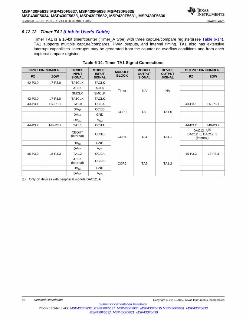
MSP430F5638, MSP430F5637, MSP430F5636, MSP430F5635MSP430F5634, MSP430F5633, MSP430F5632, MSP430F5631, MSP430F5630SLAS650E –JUNE 2010–REVISED DECEMBER 2015 www.ti.com
6.12.12 Timer TA1 (Link to User's Guide)Timer TA1 is a 16-bit timer/counter (Timer_A type) with three capture/compare registers(see Table 6-14).TA1 supports multiple capture/compares, PWM outputs, and interval timing. TA1 also has extensiveinterrupt capabilities. Interrupts may be generated from the counter on overflow conditions and from eachcapture/compare register.
Table 6-14. Timer TA1 Signal Connections
INPUT PIN NUMBER DEVICE MODULE MODULE DEVICE OUTPUT PIN NUMBERMODULEINPUT INPUT OUTPUT OUTPUTBLOCKPZ ZQW PZ ZQWSIGNAL SIGNAL SIGNAL SIGNAL42-P3.0 L7-P3.0 TA1CLK TACLK
ACLK ACLKTimer NA NA
SMCLK SMCLK42-P3.0 L7-P3.0 TA1CLK TACLK43-P3.1 H7-P3.1 TA1.0 CCI0A 43-P3.1 H7-P3.1
DVSS CCI0BCCR0 TA0 TA1.0
DVSS GNDDVCC VCC
44-P3.2 M8-P3.2 TA1.1 CCI1A 44-P3.2 M8-P3.2DAC12_A (1)
CBOUT CCI1B DAC12_0, DAC12_1(internal) CCR1 TA1 TA1.1 (internal)DVSS GNDDVCC VCC
45-P3.3 L8-P3.3 TA1.2 CCI2A 45-P3.3 L8-P3.3ACLK CCI2B(internal) CCR2 TA2 TA1.2DVSS GNDDVCC VCC
(1) Only on devices with peripheral module DAC12_A.
66 Detailed Description Copyright © 2010–2015, Texas Instruments IncorporatedSubmit Documentation Feedback
Product Folder Links: MSP430F5638 MSP430F5637 MSP430F5636 MSP430F5635 MSP430F5634 MSP430F5633MSP430F5632 MSP430F5631 MSP430F5630

MSP430F5638, MSP430F5637, MSP430F5636, MSP430F5635MSP430F5634, MSP430F5633, MSP430F5632, MSP430F5631, MSP430F5630
www.ti.com SLAS650E –JUNE 2010–REVISED DECEMBER 2015
6.12.13 Timer TA2 (Link to User's Guide)Timer TA2 is a 16-bit timer/counter (Timer_A type) with three capture/compare registers(see Table 6-15).TA2 supports multiple capture/compares, PWM outputs, and interval timing. TA2 also has extensiveinterrupt capabilities. Interrupts may be generated from the counter on overflow conditions and from eachcapture/compare register.
Table 6-15. Timer TA2 Signal Connections
INPUT PIN NUMBER DEVICE MODULE MODULE DEVICE OUTPUT PIN NUMBERMODULEINPUT INPUT OUTPUT OUTPUTBLOCKPZ ZQW PZ ZQWSIGNAL SIGNAL SIGNAL SIGNAL46-P3.4 J8-P3.4 TA2CLK TACLK
ACLK ACLKTimer NA NA
SMCLK SMCLK46-P3.4 J8-P3.4 TA2CLK TACLK47-P3.5 M9-P3.5 TA2.0 CCI0A 47-P3.5 M9-P3.5
DVSS CCI0BCCR0 TA0 TA2.0
DVSS GNDDVCC VCC
48-P3.6 L9-P3.6 TA2.1 CCI1A 48-P3.6 L9-P3.6CBOUT CCI1B(internal) CCR1 TA1 TA2.1DVSS GNDDVCC VCC
49-P3.7 M10-P3.7 TA2.2 CCI2A 49-P3.7 M10-P3.7ACLK CCI2B(internal) CCR2 TA2 TA2.2DVSS GNDDVCC VCC
Copyright © 2010–2015, Texas Instruments Incorporated Detailed Description 67Submit Documentation Feedback
Product Folder Links: MSP430F5638 MSP430F5637 MSP430F5636 MSP430F5635 MSP430F5634 MSP430F5633MSP430F5632 MSP430F5631 MSP430F5630

MSP430F5638, MSP430F5637, MSP430F5636, MSP430F5635MSP430F5634, MSP430F5633, MSP430F5632, MSP430F5631, MSP430F5630SLAS650E –JUNE 2010–REVISED DECEMBER 2015 www.ti.com
6.12.14 Timer TB0 (Link to User's Guide)Timer TB0 is a 16-bit timer/counter (Timer_B type) with seven capture/compare registers(see Table 6-16).TB0 supports multiple capture/compares, PWM outputs, and interval timing. TB0 also has extensiveinterrupt capabilities. Interrupts may be generated from the counter on overflow conditions and from eachcapture/compare register.
Table 6-16. Timer TB0 Signal Connections
INPUT PIN NUMBER DEVICE MODULE MODULE DEVICE OUTPUT PIN NUMBERMODULEINPUT INPUT OUTPUT OUTPUTBLOCKPZ ZQW PZ ZQWSIGNAL SIGNAL SIGNAL SIGNAL58-P8.0 J11-P8.0 TB0CLK TB0CLKP2MAPx (1) P2MAPx (1)
ACLK ACLKTimer NA NA
SMCLK SMCLK58-P8.0 J11-P8.0 TB0CLK TB0CLKP2MAPx (1) P2MAPx (1)
50-P4.0 J9-P4.0 TB0.0 CCI0A 50-P4.0 J9-P4.0P2MAPx (1) P2MAPx (1) TB0.0 CCI0B P2MAPx (1) P2MAPx (1)
CCR0 TB0 TB0.0 ADC12 (internal) (2)DVSS GND ADC12SHSx = 2DVCC VCC
51-P4.1 M11-P4.1 TB0.1 CCI1A 51-P4.1 M11-P4.1P2MAPx (1) P2MAPx (1) TB0.1 CCI1B P2MAPx (1) P2MAPx (1)
CCR1 TB1 TB0.1 ADC12 (internal) (2)DVSS GND ADC12SHSx = 3DVCC VCC
52-P4.2 L10-P4.2 TB0.2 CCI2A 52-P4.2 L10-P4.2P2MAPx (1) P2MAPx (1) TB0.2 CCI2B P2MAPx (1) P2MAPx (1)
DAC12_A (3)CCR2 TB2 TB0.2
DVSS GND DAC12_0, DAC12_1(internal)
DVCC VCC
53-P4.3 M12-P4.3 TB0.3 CCI3A 53-P4.3 M12-P4.3P2MAPx (1) P2MAPx (1) TB0.3 CCI3B P2MAPx (1) P2MAPx (1)
CCR3 TB3 TB0.3DVSS GNDDVCC VCC
54-P4.4 L12-P4.4 TB0.4 CCI4A 54-P4.4 L12-P4.4P2MAPx (1) P2MAPx (1) TB0.4 CCI4B P2MAPx (1) P2MAPx (1)
CCR4 TB4 TB0.4DVSS GNDDVCC VCC
55-P4.5 L11-P4.5 TB0.5 CCI5A 55-P4.5 L11-P4.5P2MAPx (1) P2MAPx (1) TB0.5 CCI5B P2MAPx (1) P2MAPx (1)
CCR5 TB5 TB0.5DVSS GNDDVCC VCC
56-P4.6 K11-P4.6 TB0.6 CCI6A 56-P4.6 K11-P4.6P2MAPx (1) P2MAPx (1) TB0.6 CCI6B P2MAPx (1) P2MAPx (1)
CCR6 TB6 TB0.6DVSS GNDDVCC VCC
(1) Timer functions selectable by the port mapping controller.(2) Only on devices with peripheral module ADC12_A.(3) Only on devices with peripheral module DAC12_A.
68 Detailed Description Copyright © 2010–2015, Texas Instruments IncorporatedSubmit Documentation Feedback
Product Folder Links: MSP430F5638 MSP430F5637 MSP430F5636 MSP430F5635 MSP430F5634 MSP430F5633MSP430F5632 MSP430F5631 MSP430F5630

MSP430F5638, MSP430F5637, MSP430F5636, MSP430F5635MSP430F5634, MSP430F5633, MSP430F5632, MSP430F5631, MSP430F5630
www.ti.com SLAS650E –JUNE 2010–REVISED DECEMBER 2015
6.12.15 Comparator_B (Link to User's Guide)The primary function of the Comparator_B module is to support precision slope analog-to-digitalconversions, battery voltage supervision, and monitoring of external analog signals.
6.12.16 ADC12_A (Link to User's Guide)The ADC12_A module supports fast 12-bit analog-to-digital conversions. The module implements a 12-bitSAR core, sample select control, reference generator, and a 16-word conversion-and-control buffer. Theconversion-and-control buffer allows up to 16 independent ADC samples to be converted and storedwithout any CPU intervention.
6.12.17 DAC12_A (Link to User's Guide)The DAC12_A module is a 12-bit R-ladder voltage-output DAC. The DAC12_A may be used in 8-bit or 12-bit mode, and may be used with the DMA controller. When multiple DAC12_A modules are present, theymay be grouped together for synchronous operation.
6.12.18 CRC16 (Link to User's Guide)The CRC16 module produces a signature based on a sequence of entered data values and can be usedfor data checking purposes. The CRC16 module signature is based on the CRC-CCITT standard.
6.12.19 Voltage Reference (REF) Module (Link to User's Guide)The REF module generates all of the critical reference voltages that can be used by the various analogperipherals in the device.
6.12.20 USB Universal Serial Bus (Link to User's Guide)The USB module is a fully integrated USB interface that is compliant with the USB 2.0 specification. Themodule supports full-speed operation of control, interrupt, and bulk transfers. The module includes anintegrated LDO, PHY, and PLL. The PLL is highly flexible and can support a wide range of input clockfrequencies. USB RAM, when not used for USB communication, can be used by the system.
6.12.21 Embedded Emulation Module (EEM) (Link to User's Guide)The EEM supports real-time in-system debugging. The L version of the EEM has the following features:• Eight hardware triggers or breakpoints on memory access• Two hardware triggers or breakpoints on CPU register write access• Up to 10 hardware triggers can be combined to form complex triggers or breakpoints• Two cycle counters• Sequencer• State storage• Clock control on module level
Copyright © 2010–2015, Texas Instruments Incorporated Detailed Description 69Submit Documentation Feedback
Product Folder Links: MSP430F5638 MSP430F5637 MSP430F5636 MSP430F5635 MSP430F5634 MSP430F5633MSP430F5632 MSP430F5631 MSP430F5630

MSP430F5638, MSP430F5637, MSP430F5636, MSP430F5635MSP430F5634, MSP430F5633, MSP430F5632, MSP430F5631, MSP430F5630SLAS650E –JUNE 2010–REVISED DECEMBER 2015 www.ti.com
6.12.22 Peripheral File MapTable 6-17 lists the register base address for all of the available peripheral modules.
Table 6-17. Peripherals
MODULE NAME BASE ADDRESS OFFSET ADDRESS RANGE (1)
Special Functions (see Table 6-18) 0100h 000h-01FhPMM (see Table 6-19) 0120h 000h-010h
Flash Control (see Table 6-20) 0140h 000h-00FhCRC16 (see Table 6-21) 0150h 000h-007h
RAM Control (see Table 6-22) 0158h 000h-001hWatchdog (see Table 6-23) 015Ch 000h-001h
UCS (see Table 6-24) 0160h 000h-01FhSYS (see Table 6-25) 0180h 000h-01Fh
Shared Reference (see Table 6-26) 01B0h 000h-001hPort Mapping Control (see Table 6-27) 01C0h 000h-003hPort Mapping Port P2 (see Table 6-27) 01D0h 000h-007h
Port P1, P2 (see Table 6-28) 0200h 000h-01FhPort P3, P4 (see Table 6-29) 0220h 000h-01FhPort P5, P6 (see Table 6-30) 0240h 000h-00BhPort P7, P8 (see Table 6-31) 0260h 000h-00Bh
Port P9 (see Table 6-32) 0280h 000h-00BhPort PJ (see Table 6-33) 0320h 000h-01Fh
Timer TA0 (see Table 6-34) 0340h 000h-02EhTimer TA1 (see Table 6-35) 0380h 000h-02EhTimer TB0 (see Table 6-36) 03C0h 000h-02EhTimer TA2 (see Table 6-37) 0400h 000h-02Eh
Battery Backup (see Table 6-38) 0480h 000h-01FhRTC_B (see Table 6-39) 04A0h 000h-01Fh
32-bit Hardware Multiplier (see Table 6-40) 04C0h 000h-02FhDMA General Control (see Table 6-41) 0500h 000h-00Fh
DMA Channel 0 (see Table 6-41) 0510h 000h-00AhDMA Channel 1 (see Table 6-41) 0520h 000h-00AhDMA Channel 2 (see Table 6-41) 0530h 000h-00AhDMA Channel 3 (see Table 6-41) 0540h 000h-00AhDMA Channel 4 (see Table 6-41) 0550h 000h-00AhDMA Channel 5 (see Table 6-41) 0560h 000h-00Ah
USCI_A0 (see Table 6-42) 05C0h 000h-01FhUSCI_B0 (see Table 6-43) 05E0h 000h-01FhUSCI_A1 (see Table 6-44) 0600h 000h-01FhUSCI_B1 (see Table 6-45) 0620h 000h-01FhADC12_A (see Table 6-46) 0700h 000h-03FhDAC12_A (see Table 6-47) 0780h 000h-01Fh
Comparator_B (see Table 6-48) 08C0h 000h-00FhUSB configuration (see Table 6-49) 0900h 000h-014h
USB control (see Table 6-50) 0920h 000h-01Fh
(1) For a detailed description of the individual control register offset addresses, see the MSP430x5xx and MSP430x6xx Family User's Guide(SLAU208).
70 Detailed Description Copyright © 2010–2015, Texas Instruments IncorporatedSubmit Documentation Feedback
Product Folder Links: MSP430F5638 MSP430F5637 MSP430F5636 MSP430F5635 MSP430F5634 MSP430F5633MSP430F5632 MSP430F5631 MSP430F5630

MSP430F5638, MSP430F5637, MSP430F5636, MSP430F5635MSP430F5634, MSP430F5633, MSP430F5632, MSP430F5631, MSP430F5630
www.ti.com SLAS650E –JUNE 2010–REVISED DECEMBER 2015
Table 6-18. Special Function Registers (Base Address: 0100h)
REGISTER DESCRIPTION REGISTER OFFSETSFR interrupt enable SFRIE1 00hSFR interrupt flag SFRIFG1 02hSFR reset pin control SFRRPCR 04h
Table 6-19. PMM Registers (Base Address: 0120h)
REGISTER DESCRIPTION REGISTER OFFSETPMM control 0 PMMCTL0 00hPMM control 1 PMMCTL1 02hSVS high-side control SVSMHCTL 04hSVS low-side control SVSMLCTL 06hPMM interrupt flags PMMIFG 0ChPMM interrupt enable PMMIE 0EhPMM power mode 5 control PM5CTL0 10h
Table 6-20. Flash Control Registers (Base Address: 0140h)
REGISTER DESCRIPTION REGISTER OFFSETFlash control 1 FCTL1 00hFlash control 3 FCTL3 04hFlash control 4 FCTL4 06h
Table 6-21. CRC16 Registers (Base Address: 0150h)
REGISTER DESCRIPTION REGISTER OFFSETCRC data input CRC16DI 00hCRC result CRC16INIRES 04h
Table 6-22. RAM Control Registers (Base Address: 0158h)
REGISTER DESCRIPTION REGISTER OFFSETRAM control 0 RCCTL0 00h
Table 6-23. Watchdog Registers (Base Address: 015Ch)
REGISTER DESCRIPTION REGISTER OFFSETWatchdog timer control WDTCTL 00h
Table 6-24. UCS Registers (Base Address: 0160h)
REGISTER DESCRIPTION REGISTER OFFSETUCS control 0 UCSCTL0 00hUCS control 1 UCSCTL1 02hUCS control 2 UCSCTL2 04hUCS control 3 UCSCTL3 06hUCS control 4 UCSCTL4 08hUCS control 5 UCSCTL5 0AhUCS control 6 UCSCTL6 0ChUCS control 7 UCSCTL7 0EhUCS control 8 UCSCTL8 10h
Copyright © 2010–2015, Texas Instruments Incorporated Detailed Description 71Submit Documentation Feedback
Product Folder Links: MSP430F5638 MSP430F5637 MSP430F5636 MSP430F5635 MSP430F5634 MSP430F5633MSP430F5632 MSP430F5631 MSP430F5630
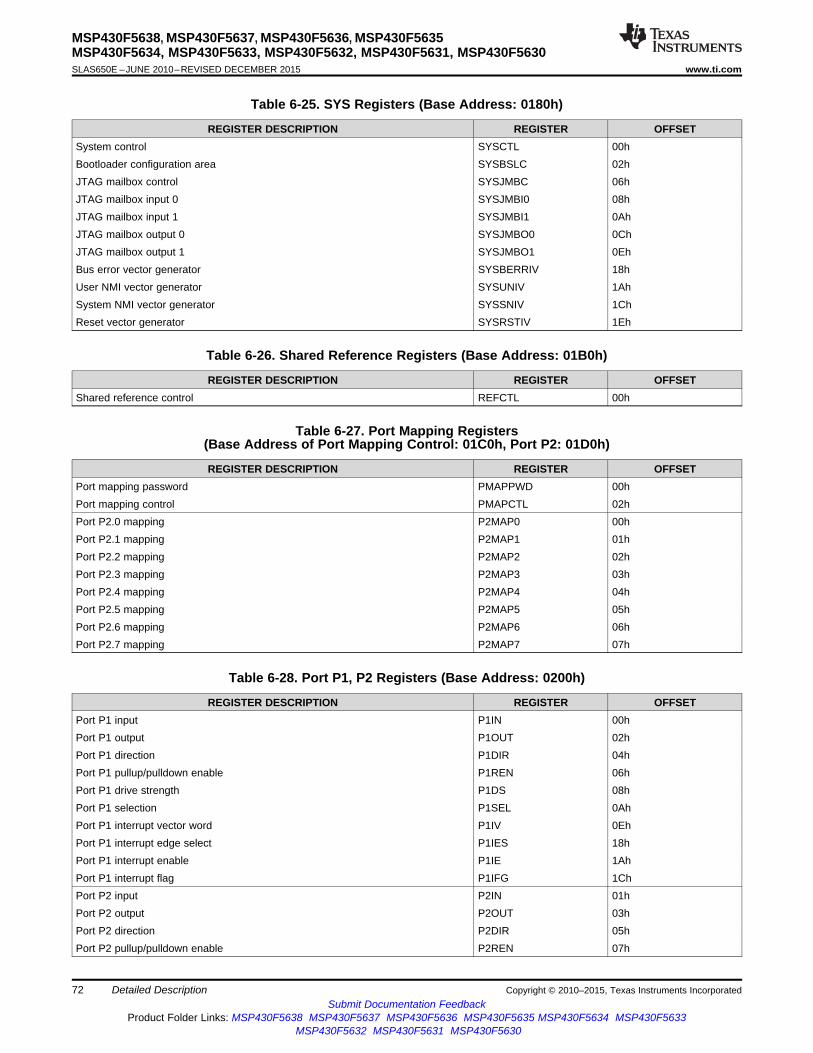
MSP430F5638, MSP430F5637, MSP430F5636, MSP430F5635MSP430F5634, MSP430F5633, MSP430F5632, MSP430F5631, MSP430F5630SLAS650E –JUNE 2010–REVISED DECEMBER 2015 www.ti.com
Table 6-25. SYS Registers (Base Address: 0180h)
REGISTER DESCRIPTION REGISTER OFFSETSystem control SYSCTL 00hBootloader configuration area SYSBSLC 02hJTAG mailbox control SYSJMBC 06hJTAG mailbox input 0 SYSJMBI0 08hJTAG mailbox input 1 SYSJMBI1 0AhJTAG mailbox output 0 SYSJMBO0 0ChJTAG mailbox output 1 SYSJMBO1 0EhBus error vector generator SYSBERRIV 18hUser NMI vector generator SYSUNIV 1AhSystem NMI vector generator SYSSNIV 1ChReset vector generator SYSRSTIV 1Eh
Table 6-26. Shared Reference Registers (Base Address: 01B0h)
REGISTER DESCRIPTION REGISTER OFFSETShared reference control REFCTL 00h
Table 6-27. Port Mapping Registers(Base Address of Port Mapping Control: 01C0h, Port P2: 01D0h)
REGISTER DESCRIPTION REGISTER OFFSETPort mapping password PMAPPWD 00hPort mapping control PMAPCTL 02hPort P2.0 mapping P2MAP0 00hPort P2.1 mapping P2MAP1 01hPort P2.2 mapping P2MAP2 02hPort P2.3 mapping P2MAP3 03hPort P2.4 mapping P2MAP4 04hPort P2.5 mapping P2MAP5 05hPort P2.6 mapping P2MAP6 06hPort P2.7 mapping P2MAP7 07h
Table 6-28. Port P1, P2 Registers (Base Address: 0200h)
REGISTER DESCRIPTION REGISTER OFFSETPort P1 input P1IN 00hPort P1 output P1OUT 02hPort P1 direction P1DIR 04hPort P1 pullup/pulldown enable P1REN 06hPort P1 drive strength P1DS 08hPort P1 selection P1SEL 0AhPort P1 interrupt vector word P1IV 0EhPort P1 interrupt edge select P1IES 18hPort P1 interrupt enable P1IE 1AhPort P1 interrupt flag P1IFG 1ChPort P2 input P2IN 01hPort P2 output P2OUT 03hPort P2 direction P2DIR 05hPort P2 pullup/pulldown enable P2REN 07h
72 Detailed Description Copyright © 2010–2015, Texas Instruments IncorporatedSubmit Documentation Feedback
Product Folder Links: MSP430F5638 MSP430F5637 MSP430F5636 MSP430F5635 MSP430F5634 MSP430F5633MSP430F5632 MSP430F5631 MSP430F5630

MSP430F5638, MSP430F5637, MSP430F5636, MSP430F5635MSP430F5634, MSP430F5633, MSP430F5632, MSP430F5631, MSP430F5630
www.ti.com SLAS650E –JUNE 2010–REVISED DECEMBER 2015
Table 6-28. Port P1, P2 Registers (Base Address: 0200h) (continued)REGISTER DESCRIPTION REGISTER OFFSET
Port P2 drive strength P2DS 09hPort P2 selection P2SEL 0BhPort P2 interrupt vector word P2IV 1EhPort P2 interrupt edge select P2IES 19hPort P2 interrupt enable P2IE 1BhPort P2 interrupt flag P2IFG 1Dh
Table 6-29. Port P3, P4 Registers (Base Address: 0220h)
REGISTER DESCRIPTION REGISTER OFFSETPort P3 input P3IN 00hPort P3 output P3OUT 02hPort P3 direction P3DIR 04hPort P3 pullup/pulldown enable P3REN 06hPort P3 drive strength P3DS 08hPort P3 selection P3SEL 0AhPort P3 interrupt vector word P3IV 0EhPort P3 interrupt edge select P3IES 18hPort P3 interrupt enable P3IE 1AhPort P3 interrupt flag P3IFG 1ChPort P4 input P4IN 01hPort P4 output P4OUT 03hPort P4 direction P4DIR 05hPort P4 pullup/pulldown enable P4REN 07hPort P4 drive strength P4DS 09hPort P4 selection P4SEL 0BhPort P4 interrupt vector word P4IV 1EhPort P4 interrupt edge select P4IES 19hPort P4 interrupt enable P4IE 1BhPort P4 interrupt flag P4IFG 1Dh
Table 6-30. Port P5, P6 Registers (Base Address: 0240h)
REGISTER DESCRIPTION REGISTER OFFSETPort P5 input P5IN 00hPort P5 output P5OUT 02hPort P5 direction P5DIR 04hPort P5 pullup/pulldown enable P5REN 06hPort P5 drive strength P5DS 08hPort P5 selection P5SEL 0AhPort P6 input P6IN 01hPort P6 output P6OUT 03hPort P6 direction P6DIR 05hPort P6 pullup/pulldown enable P6REN 07hPort P6 drive strength P6DS 09hPort P6 selection P6SEL 0Bh
Copyright © 2010–2015, Texas Instruments Incorporated Detailed Description 73Submit Documentation Feedback
Product Folder Links: MSP430F5638 MSP430F5637 MSP430F5636 MSP430F5635 MSP430F5634 MSP430F5633MSP430F5632 MSP430F5631 MSP430F5630

MSP430F5638, MSP430F5637, MSP430F5636, MSP430F5635MSP430F5634, MSP430F5633, MSP430F5632, MSP430F5631, MSP430F5630SLAS650E –JUNE 2010–REVISED DECEMBER 2015 www.ti.com
Table 6-31. Port P7, P8 Registers (Base Address: 0260h)
REGISTER DESCRIPTION REGISTER OFFSETPort P7 input P7IN 00hPort P7 output P7OUT 02hPort P7 direction P7DIR 04hPort P7 pullup/pulldown enable P7REN 06hPort P7 drive strength P7DS 08hPort P7 selection P7SEL 0AhPort P8 input P8IN 01hPort P8 output P8OUT 03hPort P8 direction P8DIR 05hPort P8 pullup/pulldown enable P8REN 07hPort P8 drive strength P8DS 09hPort P8 selection P8SEL 0Bh
Table 6-32. Port P9 Register (Base Address: 0280h)
REGISTER DESCRIPTION REGISTER OFFSETPort P9 input P9IN 00hPort P9 output P9OUT 02hPort P9 direction P9DIR 04hPort P9 pullup/pulldown enable P9REN 06hPort P9 drive strength P9DS 08hPort P9 selection P9SEL 0Ah
Table 6-33. Port J Registers (Base Address: 0320h)
REGISTER DESCRIPTION REGISTER OFFSETPort PJ input PJIN 00hPort PJ output PJOUT 02hPort PJ direction PJDIR 04hPort PJ pullup/pulldown enable PJREN 06hPort PJ drive strength PJDS 08h
Table 6-34. TA0 Registers (Base Address: 0340h)
REGISTER DESCRIPTION REGISTER OFFSETTA0 control TA0CTL 00hCapture/compare control 0 TA0CCTL0 02hCapture/compare control 1 TA0CCTL1 04hCapture/compare control 2 TA0CCTL2 06hCapture/compare control 3 TA0CCTL3 08hCapture/compare control 4 TA0CCTL4 0AhTA0 counter TA0R 10hCapture/compare 0 TA0CCR0 12hCapture/compare 1 TA0CCR1 14hCapture/compare 2 TA0CCR2 16hCapture/compare 3 TA0CCR3 18hCapture/compare 4 TA0CCR4 1AhTA0 expansion 0 TA0EX0 20hTA0 interrupt vector TA0IV 2Eh
74 Detailed Description Copyright © 2010–2015, Texas Instruments IncorporatedSubmit Documentation Feedback
Product Folder Links: MSP430F5638 MSP430F5637 MSP430F5636 MSP430F5635 MSP430F5634 MSP430F5633MSP430F5632 MSP430F5631 MSP430F5630
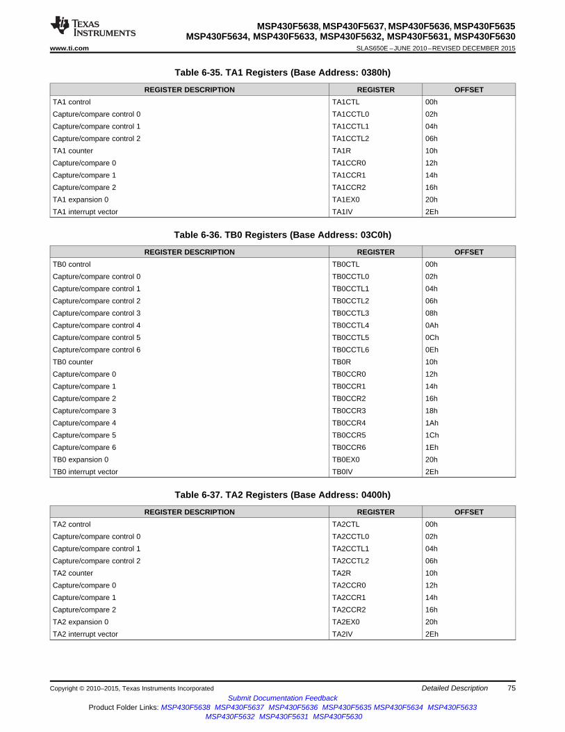
MSP430F5638, MSP430F5637, MSP430F5636, MSP430F5635MSP430F5634, MSP430F5633, MSP430F5632, MSP430F5631, MSP430F5630
www.ti.com SLAS650E –JUNE 2010–REVISED DECEMBER 2015
Table 6-35. TA1 Registers (Base Address: 0380h)
REGISTER DESCRIPTION REGISTER OFFSETTA1 control TA1CTL 00hCapture/compare control 0 TA1CCTL0 02hCapture/compare control 1 TA1CCTL1 04hCapture/compare control 2 TA1CCTL2 06hTA1 counter TA1R 10hCapture/compare 0 TA1CCR0 12hCapture/compare 1 TA1CCR1 14hCapture/compare 2 TA1CCR2 16hTA1 expansion 0 TA1EX0 20hTA1 interrupt vector TA1IV 2Eh
Table 6-36. TB0 Registers (Base Address: 03C0h)
REGISTER DESCRIPTION REGISTER OFFSETTB0 control TB0CTL 00hCapture/compare control 0 TB0CCTL0 02hCapture/compare control 1 TB0CCTL1 04hCapture/compare control 2 TB0CCTL2 06hCapture/compare control 3 TB0CCTL3 08hCapture/compare control 4 TB0CCTL4 0AhCapture/compare control 5 TB0CCTL5 0ChCapture/compare control 6 TB0CCTL6 0EhTB0 counter TB0R 10hCapture/compare 0 TB0CCR0 12hCapture/compare 1 TB0CCR1 14hCapture/compare 2 TB0CCR2 16hCapture/compare 3 TB0CCR3 18hCapture/compare 4 TB0CCR4 1AhCapture/compare 5 TB0CCR5 1ChCapture/compare 6 TB0CCR6 1EhTB0 expansion 0 TB0EX0 20hTB0 interrupt vector TB0IV 2Eh
Table 6-37. TA2 Registers (Base Address: 0400h)
REGISTER DESCRIPTION REGISTER OFFSETTA2 control TA2CTL 00hCapture/compare control 0 TA2CCTL0 02hCapture/compare control 1 TA2CCTL1 04hCapture/compare control 2 TA2CCTL2 06hTA2 counter TA2R 10hCapture/compare 0 TA2CCR0 12hCapture/compare 1 TA2CCR1 14hCapture/compare 2 TA2CCR2 16hTA2 expansion 0 TA2EX0 20hTA2 interrupt vector TA2IV 2Eh
Copyright © 2010–2015, Texas Instruments Incorporated Detailed Description 75Submit Documentation Feedback
Product Folder Links: MSP430F5638 MSP430F5637 MSP430F5636 MSP430F5635 MSP430F5634 MSP430F5633MSP430F5632 MSP430F5631 MSP430F5630
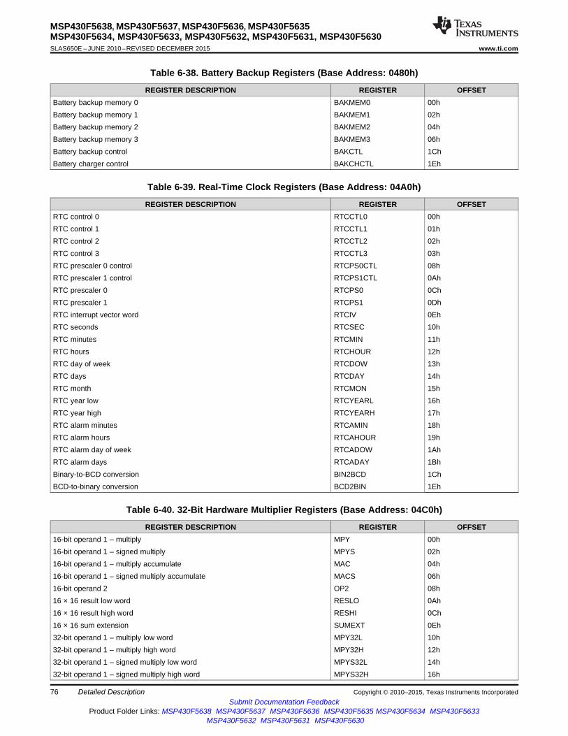
MSP430F5638, MSP430F5637, MSP430F5636, MSP430F5635MSP430F5634, MSP430F5633, MSP430F5632, MSP430F5631, MSP430F5630SLAS650E –JUNE 2010–REVISED DECEMBER 2015 www.ti.com
Table 6-38. Battery Backup Registers (Base Address: 0480h)
REGISTER DESCRIPTION REGISTER OFFSETBattery backup memory 0 BAKMEM0 00hBattery backup memory 1 BAKMEM1 02hBattery backup memory 2 BAKMEM2 04hBattery backup memory 3 BAKMEM3 06hBattery backup control BAKCTL 1ChBattery charger control BAKCHCTL 1Eh
Table 6-39. Real-Time Clock Registers (Base Address: 04A0h)
REGISTER DESCRIPTION REGISTER OFFSETRTC control 0 RTCCTL0 00hRTC control 1 RTCCTL1 01hRTC control 2 RTCCTL2 02hRTC control 3 RTCCTL3 03hRTC prescaler 0 control RTCPS0CTL 08hRTC prescaler 1 control RTCPS1CTL 0AhRTC prescaler 0 RTCPS0 0ChRTC prescaler 1 RTCPS1 0DhRTC interrupt vector word RTCIV 0EhRTC seconds RTCSEC 10hRTC minutes RTCMIN 11hRTC hours RTCHOUR 12hRTC day of week RTCDOW 13hRTC days RTCDAY 14hRTC month RTCMON 15hRTC year low RTCYEARL 16hRTC year high RTCYEARH 17hRTC alarm minutes RTCAMIN 18hRTC alarm hours RTCAHOUR 19hRTC alarm day of week RTCADOW 1AhRTC alarm days RTCADAY 1BhBinary-to-BCD conversion BIN2BCD 1ChBCD-to-binary conversion BCD2BIN 1Eh
Table 6-40. 32-Bit Hardware Multiplier Registers (Base Address: 04C0h)
REGISTER DESCRIPTION REGISTER OFFSET16-bit operand 1 – multiply MPY 00h16-bit operand 1 – signed multiply MPYS 02h16-bit operand 1 – multiply accumulate MAC 04h16-bit operand 1 – signed multiply accumulate MACS 06h16-bit operand 2 OP2 08h16 × 16 result low word RESLO 0Ah16 × 16 result high word RESHI 0Ch16 × 16 sum extension SUMEXT 0Eh32-bit operand 1 – multiply low word MPY32L 10h32-bit operand 1 – multiply high word MPY32H 12h32-bit operand 1 – signed multiply low word MPYS32L 14h32-bit operand 1 – signed multiply high word MPYS32H 16h
76 Detailed Description Copyright © 2010–2015, Texas Instruments IncorporatedSubmit Documentation Feedback
Product Folder Links: MSP430F5638 MSP430F5637 MSP430F5636 MSP430F5635 MSP430F5634 MSP430F5633MSP430F5632 MSP430F5631 MSP430F5630
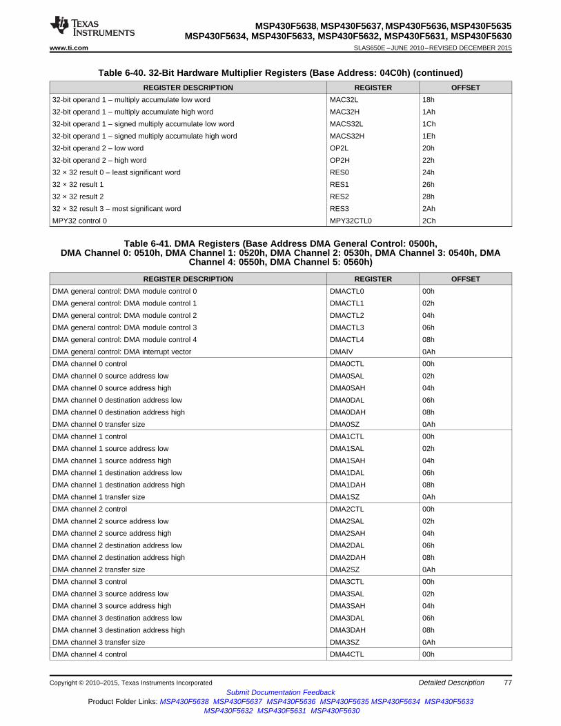
MSP430F5638, MSP430F5637, MSP430F5636, MSP430F5635MSP430F5634, MSP430F5633, MSP430F5632, MSP430F5631, MSP430F5630
www.ti.com SLAS650E –JUNE 2010–REVISED DECEMBER 2015
Table 6-40. 32-Bit Hardware Multiplier Registers (Base Address: 04C0h) (continued)REGISTER DESCRIPTION REGISTER OFFSET
32-bit operand 1 – multiply accumulate low word MAC32L 18h32-bit operand 1 – multiply accumulate high word MAC32H 1Ah32-bit operand 1 – signed multiply accumulate low word MACS32L 1Ch32-bit operand 1 – signed multiply accumulate high word MACS32H 1Eh32-bit operand 2 – low word OP2L 20h32-bit operand 2 – high word OP2H 22h32 × 32 result 0 – least significant word RES0 24h32 × 32 result 1 RES1 26h32 × 32 result 2 RES2 28h32 × 32 result 3 – most significant word RES3 2AhMPY32 control 0 MPY32CTL0 2Ch
Table 6-41. DMA Registers (Base Address DMA General Control: 0500h,DMA Channel 0: 0510h, DMA Channel 1: 0520h, DMA Channel 2: 0530h, DMA Channel 3: 0540h, DMA
Channel 4: 0550h, DMA Channel 5: 0560h)
REGISTER DESCRIPTION REGISTER OFFSETDMA general control: DMA module control 0 DMACTL0 00hDMA general control: DMA module control 1 DMACTL1 02hDMA general control: DMA module control 2 DMACTL2 04hDMA general control: DMA module control 3 DMACTL3 06hDMA general control: DMA module control 4 DMACTL4 08hDMA general control: DMA interrupt vector DMAIV 0AhDMA channel 0 control DMA0CTL 00hDMA channel 0 source address low DMA0SAL 02hDMA channel 0 source address high DMA0SAH 04hDMA channel 0 destination address low DMA0DAL 06hDMA channel 0 destination address high DMA0DAH 08hDMA channel 0 transfer size DMA0SZ 0AhDMA channel 1 control DMA1CTL 00hDMA channel 1 source address low DMA1SAL 02hDMA channel 1 source address high DMA1SAH 04hDMA channel 1 destination address low DMA1DAL 06hDMA channel 1 destination address high DMA1DAH 08hDMA channel 1 transfer size DMA1SZ 0AhDMA channel 2 control DMA2CTL 00hDMA channel 2 source address low DMA2SAL 02hDMA channel 2 source address high DMA2SAH 04hDMA channel 2 destination address low DMA2DAL 06hDMA channel 2 destination address high DMA2DAH 08hDMA channel 2 transfer size DMA2SZ 0AhDMA channel 3 control DMA3CTL 00hDMA channel 3 source address low DMA3SAL 02hDMA channel 3 source address high DMA3SAH 04hDMA channel 3 destination address low DMA3DAL 06hDMA channel 3 destination address high DMA3DAH 08hDMA channel 3 transfer size DMA3SZ 0AhDMA channel 4 control DMA4CTL 00h
Copyright © 2010–2015, Texas Instruments Incorporated Detailed Description 77Submit Documentation Feedback
Product Folder Links: MSP430F5638 MSP430F5637 MSP430F5636 MSP430F5635 MSP430F5634 MSP430F5633MSP430F5632 MSP430F5631 MSP430F5630

MSP430F5638, MSP430F5637, MSP430F5636, MSP430F5635MSP430F5634, MSP430F5633, MSP430F5632, MSP430F5631, MSP430F5630SLAS650E –JUNE 2010–REVISED DECEMBER 2015 www.ti.com
Table 6-41. DMA Registers (Base Address DMA General Control: 0500h,DMA Channel 0: 0510h, DMA Channel 1: 0520h, DMA Channel 2: 0530h, DMA Channel 3: 0540h, DMA
Channel 4: 0550h, DMA Channel 5: 0560h) (continued)REGISTER DESCRIPTION REGISTER OFFSET
DMA channel 4 source address low DMA4SAL 02hDMA channel 4 source address high DMA4SAH 04hDMA channel 4 destination address low DMA4DAL 06hDMA channel 4 destination address high DMA4DAH 08hDMA channel 4 transfer size DMA4SZ 0AhDMA channel 5 control DMA5CTL 00hDMA channel 5 source address low DMA5SAL 02hDMA channel 5 source address high DMA5SAH 04hDMA channel 5 destination address low DMA5DAL 06hDMA channel 5 destination address high DMA5DAH 08hDMA channel 5 transfer size DMA5SZ 0Ah
Table 6-42. USCI_A0 Registers (Base Address: 05C0h)
REGISTER DESCRIPTION REGISTER OFFSETUSCI control 0 UCA0CTL0 00hUSCI control 1 UCA0CTL1 01hUSCI baud rate 0 UCA0BR0 06hUSCI baud rate 1 UCA0BR1 07hUSCI modulation control UCA0MCTL 08hUSCI status UCA0STAT 0AhUSCI receive buffer UCA0RXBUF 0ChUSCI transmit buffer UCA0TXBUF 0EhUSCI LIN control UCA0ABCTL 10hUSCI IrDA transmit control UCA0IRTCTL 12hUSCI IrDA receive control UCA0IRRCTL 13hUSCI interrupt enable UCA0IE 1ChUSCI interrupt flags UCA0IFG 1DhUSCI interrupt vector word UCA0IV 1Eh
Table 6-43. USCI_B0 Registers (Base Address: 05E0h)
REGISTER DESCRIPTION REGISTER OFFSETUSCI synchronous control 0 UCB0CTL0 00hUSCI synchronous control 1 UCB0CTL1 01hUSCI synchronous bit rate 0 UCB0BR0 06hUSCI synchronous bit rate 1 UCB0BR1 07hUSCI synchronous status UCB0STAT 0AhUSCI synchronous receive buffer UCB0RXBUF 0ChUSCI synchronous transmit buffer UCB0TXBUF 0EhUSCI I2C own address UCB0I2COA 10hUSCI I2C slave address UCB0I2CSA 12hUSCI interrupt enable UCB0IE 1ChUSCI interrupt flags UCB0IFG 1DhUSCI interrupt vector word UCB0IV 1Eh
78 Detailed Description Copyright © 2010–2015, Texas Instruments IncorporatedSubmit Documentation Feedback
Product Folder Links: MSP430F5638 MSP430F5637 MSP430F5636 MSP430F5635 MSP430F5634 MSP430F5633MSP430F5632 MSP430F5631 MSP430F5630

MSP430F5638, MSP430F5637, MSP430F5636, MSP430F5635MSP430F5634, MSP430F5633, MSP430F5632, MSP430F5631, MSP430F5630
www.ti.com SLAS650E –JUNE 2010–REVISED DECEMBER 2015
Table 6-44. USCI_A1 Registers (Base Address: 0600h)
REGISTER DESCRIPTION REGISTER OFFSETUSCI control 0 UCA1CTL0 00hUSCI control 1 UCA1CTL1 01hUSCI baud rate 0 UCA1BR0 06hUSCI baud rate 1 UCA1BR1 07hUSCI modulation control UCA1MCTL 08hUSCI status UCA1STAT 0AhUSCI receive buffer UCA1RXBUF 0ChUSCI transmit buffer UCA1TXBUF 0EhUSCI LIN control UCA1ABCTL 10hUSCI IrDA transmit control UCA1IRTCTL 12hUSCI IrDA receive control UCA1IRRCTL 13hUSCI interrupt enable UCA1IE 1ChUSCI interrupt flags UCA1IFG 1DhUSCI interrupt vector word UCA1IV 1Eh
Table 6-45. USCI_B1 Registers (Base Address: 0620h)
REGISTER DESCRIPTION REGISTER OFFSETUSCI synchronous control 0 UCB1CTL0 00hUSCI synchronous control 1 UCB1CTL1 01hUSCI synchronous bit rate 0 UCB1BR0 06hUSCI synchronous bit rate 1 UCB1BR1 07hUSCI synchronous status UCB1STAT 0AhUSCI synchronous receive buffer UCB1RXBUF 0ChUSCI synchronous transmit buffer UCB1TXBUF 0EhUSCI I2C own address UCB1I2COA 10hUSCI I2C slave address UCB1I2CSA 12hUSCI interrupt enable UCB1IE 1ChUSCI interrupt flags UCB1IFG 1DhUSCI interrupt vector word UCB1IV 1Eh
Table 6-46. ADC12_A Registers (Base Address: 0700h)
REGISTER DESCRIPTION REGISTER OFFSETADC12 control 0 ADC12CTL0 00hADC12 control 1 ADC12CTL1 02hADC12 control 2 ADC12CTL2 04hInterrupt flag ADC12IFG 0AhInterrupt enable ADC12IE 0ChInterrupt vector word ADC12IV 0EhADC memory control 0 ADC12MCTL0 10hADC memory control 1 ADC12MCTL1 11hADC memory control 2 ADC12MCTL2 12hADC memory control 3 ADC12MCTL3 13hADC memory control 4 ADC12MCTL4 14hADC memory control 5 ADC12MCTL5 15hADC memory control 6 ADC12MCTL6 16hADC memory control 7 ADC12MCTL7 17hADC memory control 8 ADC12MCTL8 18h
Copyright © 2010–2015, Texas Instruments Incorporated Detailed Description 79Submit Documentation Feedback
Product Folder Links: MSP430F5638 MSP430F5637 MSP430F5636 MSP430F5635 MSP430F5634 MSP430F5633MSP430F5632 MSP430F5631 MSP430F5630

MSP430F5638, MSP430F5637, MSP430F5636, MSP430F5635MSP430F5634, MSP430F5633, MSP430F5632, MSP430F5631, MSP430F5630SLAS650E –JUNE 2010–REVISED DECEMBER 2015 www.ti.com
Table 6-46. ADC12_A Registers (Base Address: 0700h) (continued)REGISTER DESCRIPTION REGISTER OFFSET
ADC memory control 9 ADC12MCTL9 19hADC memory control 10 ADC12MCTL10 1AhADC memory control 11 ADC12MCTL11 1BhADC memory control 12 ADC12MCTL12 1ChADC memory control 13 ADC12MCTL13 1DhADC memory control 14 ADC12MCTL14 1EhADC memory control 15 ADC12MCTL15 1FhConversion memory 0 ADC12MEM0 20hConversion memory 1 ADC12MEM1 22hConversion memory 2 ADC12MEM2 24hConversion memory 3 ADC12MEM3 26hConversion memory 4 ADC12MEM4 28hConversion memory 5 ADC12MEM5 2AhConversion memory 6 ADC12MEM6 2ChConversion memory 7 ADC12MEM7 2EhConversion memory 8 ADC12MEM8 30hConversion memory 9 ADC12MEM9 32hConversion memory 10 ADC12MEM10 34hConversion memory 11 ADC12MEM11 36hConversion memory 12 ADC12MEM12 38hConversion memory 13 ADC12MEM13 3AhConversion memory 14 ADC12MEM14 3ChConversion memory 15 ADC12MEM15 3Eh
Table 6-47. DAC12_A Registers (Base Address: 0780h)
REGISTER DESCRIPTION REGISTER OFFSETDAC12_A channel 0 control 0 DAC12_0CTL0 00hDAC12_A channel 0 control 1 DAC12_0CTL1 02hDAC12_A channel 0 data DAC12_0DAT 04hDAC12_A channel 0 calibration control DAC12_0CALCTL 06hDAC12_A channel 0 calibration data DAC12_0CALDAT 08hDAC12_A channel 1 control 0 DAC12_1CTL0 10hDAC12_A channel 1 control 1 DAC12_1CTL1 12hDAC12_A channel 1 data DAC12_1DAT 14hDAC12_A channel 1 calibration control DAC12_1CALCTL 16hDAC12_A channel 1 calibration data DAC12_1CALDAT 18hDAC12_A interrupt vector word DAC12IV 1Eh
Table 6-48. Comparator_B Registers (Base Address: 08C0h)
REGISTER DESCRIPTION REGISTER OFFSETComp_B control 0 CBCTL0 00hComp_B control 1 CBCTL1 02hComp_B control 2 CBCTL2 04hComp_B control 3 CBCTL3 06hComp_B interrupt CBINT 0ChComp_B interrupt vector word CBIV 0Eh
80 Detailed Description Copyright © 2010–2015, Texas Instruments IncorporatedSubmit Documentation Feedback
Product Folder Links: MSP430F5638 MSP430F5637 MSP430F5636 MSP430F5635 MSP430F5634 MSP430F5633MSP430F5632 MSP430F5631 MSP430F5630
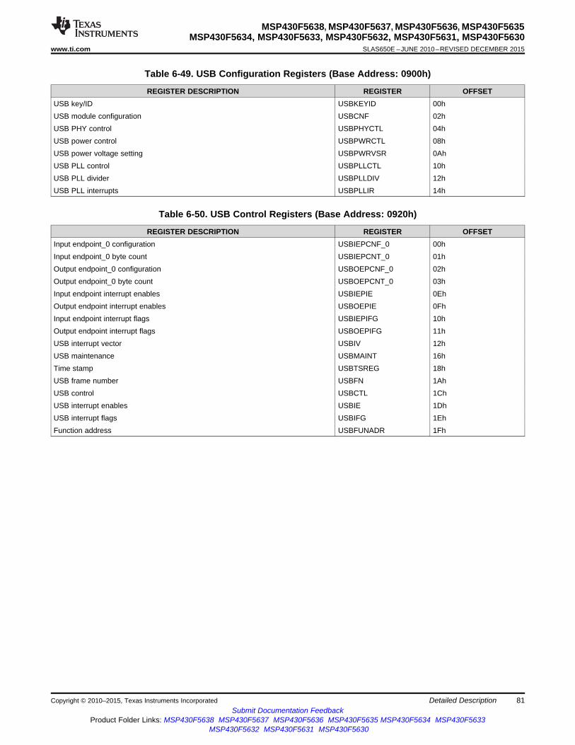
MSP430F5638, MSP430F5637, MSP430F5636, MSP430F5635MSP430F5634, MSP430F5633, MSP430F5632, MSP430F5631, MSP430F5630
www.ti.com SLAS650E –JUNE 2010–REVISED DECEMBER 2015
Table 6-49. USB Configuration Registers (Base Address: 0900h)
REGISTER DESCRIPTION REGISTER OFFSETUSB key/ID USBKEYID 00hUSB module configuration USBCNF 02hUSB PHY control USBPHYCTL 04hUSB power control USBPWRCTL 08hUSB power voltage setting USBPWRVSR 0AhUSB PLL control USBPLLCTL 10hUSB PLL divider USBPLLDIV 12hUSB PLL interrupts USBPLLIR 14h
Table 6-50. USB Control Registers (Base Address: 0920h)
REGISTER DESCRIPTION REGISTER OFFSETInput endpoint_0 configuration USBIEPCNF_0 00hInput endpoint_0 byte count USBIEPCNT_0 01hOutput endpoint_0 configuration USBOEPCNF_0 02hOutput endpoint_0 byte count USBOEPCNT_0 03hInput endpoint interrupt enables USBIEPIE 0EhOutput endpoint interrupt enables USBOEPIE 0FhInput endpoint interrupt flags USBIEPIFG 10hOutput endpoint interrupt flags USBOEPIFG 11hUSB interrupt vector USBIV 12hUSB maintenance USBMAINT 16hTime stamp USBTSREG 18hUSB frame number USBFN 1AhUSB control USBCTL 1ChUSB interrupt enables USBIE 1DhUSB interrupt flags USBIFG 1EhFunction address USBFUNADR 1Fh
Copyright © 2010–2015, Texas Instruments Incorporated Detailed Description 81Submit Documentation Feedback
Product Folder Links: MSP430F5638 MSP430F5637 MSP430F5636 MSP430F5635 MSP430F5634 MSP430F5633MSP430F5632 MSP430F5631 MSP430F5630

P1.0/TA0CLK/ACLKP1.1/TA0.0P1.2/TA0.1P1.3/TA0.2P1.4/TA0.3P1.5/TA0.4P1.6/TA0.1P1.7/TA0.2
Direction0: Input1: Output
P1SEL.x
P1DIR.x
P1IN.x
P1IRQ.x
EN
Module X IN
1
0
Module X OUT
P1OUT.x
InterruptEdgeSelect
Q
EN
Set
P1SEL.x
P1IES.x
P1IFG.x
P1IE.x
1
0DVSS
DVCC
P1REN.xPad Logic
1
P1DS.x0: Low drive1: High drive
D
MSP430F5638, MSP430F5637, MSP430F5636, MSP430F5635MSP430F5634, MSP430F5633, MSP430F5632, MSP430F5631, MSP430F5630SLAS650E –JUNE 2010–REVISED DECEMBER 2015 www.ti.com
6.13 Input/Output Schematics
6.13.1 Port P1, P1.0 to P1.7, Input/Output With Schmitt Trigger
Figure 6-2. Port P1 (P1.0 to P1.7) Schematic
82 Detailed Description Copyright © 2010–2015, Texas Instruments IncorporatedSubmit Documentation Feedback
Product Folder Links: MSP430F5638 MSP430F5637 MSP430F5636 MSP430F5635 MSP430F5634 MSP430F5633MSP430F5632 MSP430F5631 MSP430F5630

MSP430F5638, MSP430F5637, MSP430F5636, MSP430F5635MSP430F5634, MSP430F5633, MSP430F5632, MSP430F5631, MSP430F5630
www.ti.com SLAS650E –JUNE 2010–REVISED DECEMBER 2015
Table 6-51. Port P1 (P1.0 to P1.7) Pin Functions
CONTROL BITS OR SIGNALSPIN NAME (P1.x) x FUNCTION
P1DIR.x P1SEL.xP1.0/TA0CLK/ACLK 0 P1.0 (I/O) I: 0; O: 1 0
Timer TA0.TA0CLK 0 1ACLK 1 1
P1.1/TA0.0 1 P1.1 (I/O) I: 0; O: 1 0Timer TA0.CCI0A capture input 0 1Timer TA0.0 output 1 1
P1.2/TA0.1 2 P1.2 (I/O) I: 0; O: 1 0Timer TA0.CCI1A capture input 0 1Timer TA0.1 output 1 1
P1.3/TA0.2 3 P1.3 (I/O) I: 0; O: 1 0Timer TA0.CCI2A capture input 0 1Timer TA0.2 output 1 1
P1.4/TA0.3 4 P1.4 (I/O) I: 0; O: 1 0Timer TA0.CCI3A capture input 0 1Timer TA0.3 output 1 1
P1.5/TA0.4 5 P1.5 (I/O) I: 0; O: 1 0Timer TA0.CCI4A capture input 0 1Timer TA0.4 output 1 1
P1.6/TA0.1 6 P1.6 (I/O) I: 0; O: 1 0Timer TA0.CCI1B capture input 0 1Timer TA0.1 output 1 1
P1.7/TA0.2 7 P1.7 (I/O) I: 0; O: 1 0Timer TA0.CCI2B capture input 0 1Timer TA0.2 output 1 1
Copyright © 2010–2015, Texas Instruments Incorporated Detailed Description 83Submit Documentation Feedback
Product Folder Links: MSP430F5638 MSP430F5637 MSP430F5636 MSP430F5635 MSP430F5634 MSP430F5633MSP430F5632 MSP430F5631 MSP430F5630

P2.0/P2MAP0P2.1/P2MAP1P2.2/P2MAP2P2.3/P2MAP3P2.4/P2MAP4P2.5/P2MAP5P2.6/P2MAP6P2.7/P2MAP7
Direction0: Input1: Output
P2SEL.x
1
0P2DIR.x
P2IN.x
P2IRQ.x
EN
To Port Mapping
1
0
From Port Mapping
P2OUT.x
InterruptEdgeSelect
Q
EN
Set
P2SEL.x
P2IES.x
P2IFG.x
P2IE.x
1
0DVSS
DVCC
P2REN.xPad Logic
1
P2DS.x0: Low drive1: High drive
D
From Port Mapping
MSP430F5638, MSP430F5637, MSP430F5636, MSP430F5635MSP430F5634, MSP430F5633, MSP430F5632, MSP430F5631, MSP430F5630SLAS650E –JUNE 2010–REVISED DECEMBER 2015 www.ti.com
6.13.2 Port P2, P2.0 to P2.7, Input/Output With Schmitt Trigger
Figure 6-3. Port P2 (P2.0 to P2.7) Schematic
84 Detailed Description Copyright © 2010–2015, Texas Instruments IncorporatedSubmit Documentation Feedback
Product Folder Links: MSP430F5638 MSP430F5637 MSP430F5636 MSP430F5635 MSP430F5634 MSP430F5633MSP430F5632 MSP430F5631 MSP430F5630

MSP430F5638, MSP430F5637, MSP430F5636, MSP430F5635MSP430F5634, MSP430F5633, MSP430F5632, MSP430F5631, MSP430F5630
www.ti.com SLAS650E –JUNE 2010–REVISED DECEMBER 2015
Table 6-52. Port P2 (P2.0 to P2.7) Pin Functions
CONTROL BITS OR SIGNALS (1)PIN NAME (P2.x) x FUNCTION
P2DIR.x P2SEL.x P2MAPxP2.0/P2MAP0 0 P2.0 (I/O) I: 0; O: 1 0
Mapped secondary digital function X 1 ≤ 19P2.1/P2MAP1 1 P2.1 (I/O) I: 0; O: 1 0
Mapped secondary digital function X 1 ≤ 19P2.2/P2MAP2 2 P2.2 (I/O) I: 0; O: 1 0
Mapped secondary digital function X 1 ≤ 19P2.3/P2MAP3 3 P2.3 (I/O) I: 0; O: 1 0
Mapped secondary digital function X 1 ≤ 19P2.4/P2MAP4 4 P2.4 (I/O) I: 0; O: 1 0
Mapped secondary digital function X 1 ≤ 19P2.5/P2MAP5 5 P2.5 (I/O I: 0; O: 1 0
Mapped secondary digital function X 1 ≤ 19P2.6/P2MAP6 6 P2.6 (I/O) I: 0; O: 1 0
Mapped secondary digital function X 1 ≤ 19P2.7/P2MAP7 7 P2.7 (I/O) I: 0; O: 1 0
Mapped secondary digital function X 1 ≤ 19
(1) X = Don't care
Copyright © 2010–2015, Texas Instruments Incorporated Detailed Description 85Submit Documentation Feedback
Product Folder Links: MSP430F5638 MSP430F5637 MSP430F5636 MSP430F5635 MSP430F5634 MSP430F5633MSP430F5632 MSP430F5631 MSP430F5630

P3.0/TA1CLK/CBOUTP3.1/TA1.0P3.2/TA1.1P3.3/TA1.2P3.4/TA2CLK/SMCLKP3.5/TA2.0P3.6/TA2.1P3.7/TA2.2
Direction0: Input1: Output
P3SEL.x
P3DIR.x
P3IN.x
EN
Module X IN
1
0
Module X OUT
P3OUT.x
1
0DVSS
DVCC
P3REN.xPad Logic
1
P3DS.x0: Low drive1: High drive
D
P3IRQ.x
InterruptEdgeSelect
Q
EN
Set
P3SEL.x
P3IES.x
P3IFG.x
P3IE.x
MSP430F5638, MSP430F5637, MSP430F5636, MSP430F5635MSP430F5634, MSP430F5633, MSP430F5632, MSP430F5631, MSP430F5630SLAS650E –JUNE 2010–REVISED DECEMBER 2015 www.ti.com
6.13.3 Port P3, P3.0 to P3.7, Input/Output With Schmitt Trigger
Figure 6-4. Port P3 (P3.0 to P3.7) Schematic
86 Detailed Description Copyright © 2010–2015, Texas Instruments IncorporatedSubmit Documentation Feedback
Product Folder Links: MSP430F5638 MSP430F5637 MSP430F5636 MSP430F5635 MSP430F5634 MSP430F5633MSP430F5632 MSP430F5631 MSP430F5630

MSP430F5638, MSP430F5637, MSP430F5636, MSP430F5635MSP430F5634, MSP430F5633, MSP430F5632, MSP430F5631, MSP430F5630
www.ti.com SLAS650E –JUNE 2010–REVISED DECEMBER 2015
Table 6-53. Port P3 (P3.0 to P3.7) Pin Functions
CONTROL BITS OR SIGNALSPIN NAME (P3.x) x FUNCTION
P3DIR.x P3SEL.xP3.0/TA1CLK/CBOUT 0 P3.0 (I/O) I: 0; O: 1 0
Timer TA1.TA1CLK 0 1CBOUT 1 1
P3.1/TA1.0 1 P3.1 (I/O) I: 0; O: 1 0Timer TA1.CCI0A capture input 0 1Timer TA1.0 output 1 1
P3.2/TA1.1 2 P3.2 (I/O) I: 0; O: 1 0Timer TA1.CCI1A capture input 0 1Timer TA1.1 output 1 1
P3.3/TA1.2 3 P3.3 (I/O) I: 0; O: 1 0Timer TA1.CCI2A capture input 0 1Timer TA1.2 output 1 1
P3.4/TA2CLK/SMCLK 4 P3.4 (I/O) I: 0; O: 1 0Timer TA2.TA2CLK 0 1SMCLK 1 1
P3.5/TA2.0 5 P3.5 (I/O) I: 0; O: 1 0Timer TA2.CCI0A capture input 0 1Timer TA2.0 output 1 1
P3.6/TA2.1 6 P3.6 (I/O) I: 0; O: 1 0Timer TA2.CCI1A capture input 0 1Timer TA2.1 output 1 1
P3.7/TA2.2 7 P3.7 (I/O) I: 0; O: 1 0Timer TA2.CCI2A capture input 0 1Timer TA2.2 output 1 1
Copyright © 2010–2015, Texas Instruments Incorporated Detailed Description 87Submit Documentation Feedback
Product Folder Links: MSP430F5638 MSP430F5637 MSP430F5636 MSP430F5635 MSP430F5634 MSP430F5633MSP430F5632 MSP430F5631 MSP430F5630

P4.0/TB0.0P4.1/TB0.1P4.2/TB0.2P4.3/TB0.3P4.4/TB0.4P4.5/TB0.5P4.6/TB0.6P4.7/TB0OUTH/SVMOUT
Direction0: Input1: Output
P4SEL.x
P4DIR.x
P4IN.x
EN
Module X IN
1
0
Module X OUT
P4OUT.x
1
0DVSS
DVCC
P4REN.xPad Logic
1
P4DS.x0: Low drive1: High drive
D
P4IRQ.x
InterruptEdgeSelect
Q
EN
Set
P4SEL.x
P4IES.x
P4IFG.x
P4IE.x
MSP430F5638, MSP430F5637, MSP430F5636, MSP430F5635MSP430F5634, MSP430F5633, MSP430F5632, MSP430F5631, MSP430F5630SLAS650E –JUNE 2010–REVISED DECEMBER 2015 www.ti.com
6.13.4 Port P4, P4.0 to P4.7, Input/Output With Schmitt Trigger
Figure 6-5. Port P4 (P4.0 to P4.7) Schematic
88 Detailed Description Copyright © 2010–2015, Texas Instruments IncorporatedSubmit Documentation Feedback
Product Folder Links: MSP430F5638 MSP430F5637 MSP430F5636 MSP430F5635 MSP430F5634 MSP430F5633MSP430F5632 MSP430F5631 MSP430F5630

MSP430F5638, MSP430F5637, MSP430F5636, MSP430F5635MSP430F5634, MSP430F5633, MSP430F5632, MSP430F5631, MSP430F5630
www.ti.com SLAS650E –JUNE 2010–REVISED DECEMBER 2015
Table 6-54. Port P4 (P4.0 to P4.7) Pin Functions
CONTROL BITS OR SIGNALSPIN NAME (P4.x) x FUNCTION
P4DIR.x P4SEL.xP4.0/TB0.0 0 P4.0 (I/O) I: 0; O: 1 0
Timer TB0.CCI0A capture input 0 1Timer TB0.0 output (1) 1 1
P4.1/TB0.1 1 P4.1 (I/O) I: 0; O: 1 0Timer TB0.CCI1A capture input 0 1Timer TB0.1 output (1) 1 1
P4.2/TB0.2 2 P4.2 (I/O) I: 0; O: 1 0Timer TB0.CCI2A capture input 0 1Timer TB0.2 output (1) 1 1
P4.3/TB0.3 3 P4.3 (I/O) I: 0; O: 1 0Timer TB0.CCI3A capture input 0 1Timer TB0.3 output (1) 1 1
P4.4/TB0.4 4 P4.4 (I/O) I: 0; O: 1 0Timer TB0.CCI4A capture input 0 1Timer TB0.4 output (1) 1 1
P4.5/TB0.5 5 P4.5 (I/O) I: 0; O: 1 0Timer TB0.CCI5A capture input 0 1Timer TB0.5 output (1) 1 1
P4.6/TB0.6 6 P4.6 (I/O) I: 0; O: 1 0Timer TB0.CCI6A capture input 0 1Timer TB0.6 output (1) 1 1
P4.7/TB0OUTH/ 7 P4.7 (I/O) I: 0; O: 1 0SVMOUT Timer TB0.TB0OUTH 0 1
SVMOUT 1 1
(1) Setting TB0OUTH causes all Timer_B configured outputs to be set to high impedance.
Copyright © 2010–2015, Texas Instruments Incorporated Detailed Description 89Submit Documentation Feedback
Product Folder Links: MSP430F5638 MSP430F5637 MSP430F5636 MSP430F5635 MSP430F5634 MSP430F5633MSP430F5632 MSP430F5631 MSP430F5630

P5.0/VREF+/VeREF+P5.1/VREF–/VeREF–P5SEL.x
1
0P5DIR.x
P5IN.x
EN
Module X IN
1
0
Module X OUT
P5OUT.x
1
0DVSS
DVCC
P5REN.x
Pad Logic
1
P5DS.x0: Low drive1: High drive
D
BusKeeper
To/FromReference
MSP430F5638, MSP430F5637, MSP430F5636, MSP430F5635MSP430F5634, MSP430F5633, MSP430F5632, MSP430F5631, MSP430F5630SLAS650E –JUNE 2010–REVISED DECEMBER 2015 www.ti.com
6.13.5 Port P5, P5.0 and P5.1, Input/Output With Schmitt Trigger
Figure 6-6. Port P5 (P5.0 and P5.1) Schematic
Table 6-55. Port P5 (P5.0 and P5.1) Pin Functions
CONTROL BITS OR SIGNALS (1)PIN NAME (P5.x) x FUNCTION
P5DIR.x P5SEL.x REFOUTP5.0/VREF+/VeREF+ 0 P5.0 (I/O) (2) I: 0; O: 1 0 X
VeREF+ (3) X 1 0VREF+ (4) X 1 1
P5.1/VREF-/VeREF- 1 P5.1 (I/O) (2) I: 0; O: 1 0 XVeREF- (5) X 1 0VREF- (6) X 1 1
(1) X = Don't care(2) Default condition(3) Setting the P5SEL.0 bit disables the output driver and the input Schmitt trigger to prevent parasitic cross currents when applying analog
signals. An external voltage can be applied to VeREF+ and used as the reference for the ADC12_A, Comparator_B, or DAC12_A.(4) Setting the P5SEL.0 bit disables the output driver and the input Schmitt trigger to prevent parasitic cross currents when applying analog
signals. The ADC12_A, VREF+ reference is available at the pin.(5) Setting the P5SEL.1 bit disables the output driver and the input Schmitt trigger to prevent parasitic cross currents when applying analog
signals. An external voltage can be applied to VeREF- and used as the reference for the ADC12_A, Comparator_B, or DAC12_A.(6) Setting the P5SEL.1 bit disables the output driver and the input Schmitt trigger to prevent parasitic cross currents when applying analog
signals. The ADC12_A, VREF- reference is available at the pin.
90 Detailed Description Copyright © 2010–2015, Texas Instruments IncorporatedSubmit Documentation Feedback
Product Folder Links: MSP430F5638 MSP430F5637 MSP430F5636 MSP430F5635 MSP430F5634 MSP430F5633MSP430F5632 MSP430F5631 MSP430F5630

P5.2P5.3P5.4P5.5P5.6/ADC12CLK/DMAE0P5.7/RTCCLK
Direction0: Input1: Output
P5SEL.x
P5DIR.x
P5IN.x
EN
Module X IN
1
0
Module X OUT
P5OUT.x
1
0DVSS
DVCC
P5REN.xPad Logic
1
P5DS.x0: Low drive1: High drive
D
MSP430F5638, MSP430F5637, MSP430F5636, MSP430F5635MSP430F5634, MSP430F5633, MSP430F5632, MSP430F5631, MSP430F5630
www.ti.com SLAS650E –JUNE 2010–REVISED DECEMBER 2015
6.13.6 Port P5, P5.2 to P5.7, Input/Output With Schmitt Trigger
Figure 6-7. Port P5 (P5.2 to P5.7) Schematic
Table 6-56. Port P5 (P5.2 to P5.7) Pin Functions
CONTROL BITS OR SIGNALSPIN NAME (P5.x) x FUNCTION
P5DIR.x P5SEL.xP5.2 2 P5.2 (I/O) I: 0; O: 1 0P5.3 3 P5.3 (I/O) I: 0; O: 1 0P5.4 4 P5.4 (I/O) I: 0; O: 1 0P5.5 5 P5.5 (I/O) I: 0; O: 1 0P5.6/ADC12CLK/DMAE0 6 P5.6 (I/O) I: 0; O: 1 0
ADC12CLK 1 1DMAE0 0 1
P5.7/RTCCLK 7 P5.7 (I/O) I: 0; O: 1 0RTCCLK 1 1
Copyright © 2010–2015, Texas Instruments Incorporated Detailed Description 91Submit Documentation Feedback
Product Folder Links: MSP430F5638 MSP430F5637 MSP430F5636 MSP430F5635 MSP430F5634 MSP430F5633MSP430F5632 MSP430F5631 MSP430F5630
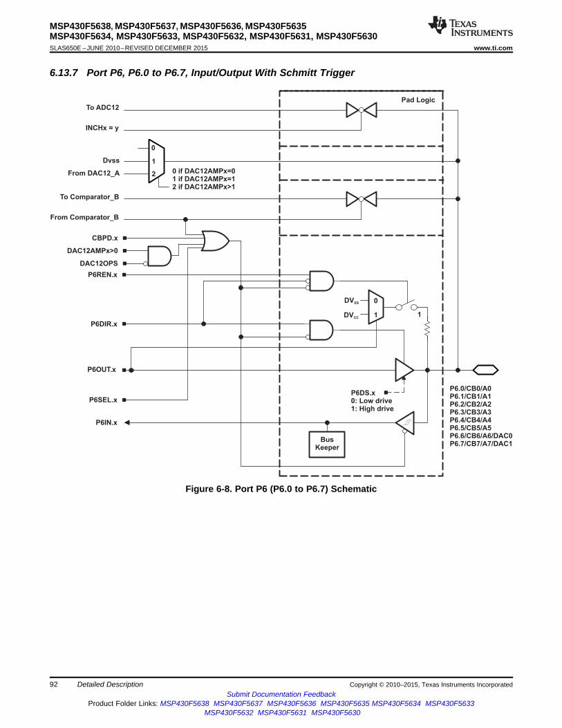
P6SEL.x
P6DIR.x
P6IN.x
P6OUT.x
1
0DVSS
DVCC
P6REN.x
Pad Logic
1
P6DS.x0: Low drive1: High drive
BusKeeper
To ADC12
P6.0/CB0/A0P6.1/CB1/A1P6.2/CB2/A2P6.3/CB3/A3P6.4/CB4/A4P6.5/CB5/A5P6.6/CB6/A6/DAC0P6.7/CB7/A7/DAC1
INCHx = y
From DAC12_A
To Comparator_B
From Comparator_B
CBPD.x
0
1
2
Dvss
0 if DAC12AMPx=01 if DAC12AMPx=12 if DAC12AMPx>1
DAC12AMPx>0
DAC12OPS
MSP430F5638, MSP430F5637, MSP430F5636, MSP430F5635MSP430F5634, MSP430F5633, MSP430F5632, MSP430F5631, MSP430F5630SLAS650E –JUNE 2010–REVISED DECEMBER 2015 www.ti.com
6.13.7 Port P6, P6.0 to P6.7, Input/Output With Schmitt Trigger
Figure 6-8. Port P6 (P6.0 to P6.7) Schematic
92 Detailed Description Copyright © 2010–2015, Texas Instruments IncorporatedSubmit Documentation Feedback
Product Folder Links: MSP430F5638 MSP430F5637 MSP430F5636 MSP430F5635 MSP430F5634 MSP430F5633MSP430F5632 MSP430F5631 MSP430F5630

MSP430F5638, MSP430F5637, MSP430F5636, MSP430F5635MSP430F5634, MSP430F5633, MSP430F5632, MSP430F5631, MSP430F5630
www.ti.com SLAS650E –JUNE 2010–REVISED DECEMBER 2015
Table 6-57. Port P6 (P6.0 to P6.7) Pin Functions
CONTROL BITS OR SIGNALS (1)PIN NAME (P6.x) x FUNCTION
P6DIR.x P6SEL.x CBPD.x DAC12OPS DAC12AMPxP6.0/CB0/A0 0 P6.0 (I/O) I: 0; O: 1 0 0 n/a n/a
CB0 X X 1 n/a n/aA0 (2) (3) X 1 X n/a n/a
P6.1/CB1/A1 1 P6.1 (I/O) I: 0; O: 1 0 0 n/a n/aCB1 X X 1 n/a n/aA1 (2) (3) X 1 X n/a n/a
P6.2/CB2/A2 2 P6.2 (I/O) I: 0; O: 1 0 0 n/a n/aCB2 X X 1 n/a n/aA2 (2) (3) X 1 X n/a n/a
P6.3/CB3/A3 3 P6.3 (I/O) I: 0; O: 1 0 0 n/a n/aCB3 X X 1 n/a n/aA3 (2) (3) X 1 X n/a n/a
P6.4/CB4/A4 4 P6.4 (I/O) I: 0; O: 1 0 0 n/a n/aCB4 X X 1 n/a n/aA4 (2) (3) X 1 X n/a n/a
P6.5/CB5/A5 5 P6.5 (I/O) I: 0; O: 1 0 0 n/a n/aCB5 X X 1 n/a n/aA5 (2) (3) X 1 X n/a n/a
P6.6/CB6/A6/DAC0 6 P6.6 (I/O) I: 0; O: 1 0 0 X 0CB6 X X 1 X 0A6 (2) (3) X 1 X X 0DAC0 X X X 0 >1
P6.7/CB7/A7/DAC1 7 P6.7 (I/O) I: 0; O: 1 0 0 X 0CB7 X X 1 X 0A7 (2) (3) X 1 X X 0DAC1 X X X 0 >1
(1) X = Don't care(2) Setting the P6SEL.x bit disables the output driver and the input Schmitt trigger to prevent parasitic cross currents when applying analog
signals.(3) The ADC12_A channel Ax is connected internally to AVSS if not selected by the respective INCHx bits.
Copyright © 2010–2015, Texas Instruments Incorporated Detailed Description 93Submit Documentation Feedback
Product Folder Links: MSP430F5638 MSP430F5637 MSP430F5636 MSP430F5635 MSP430F5634 MSP430F5633MSP430F5632 MSP430F5631 MSP430F5630
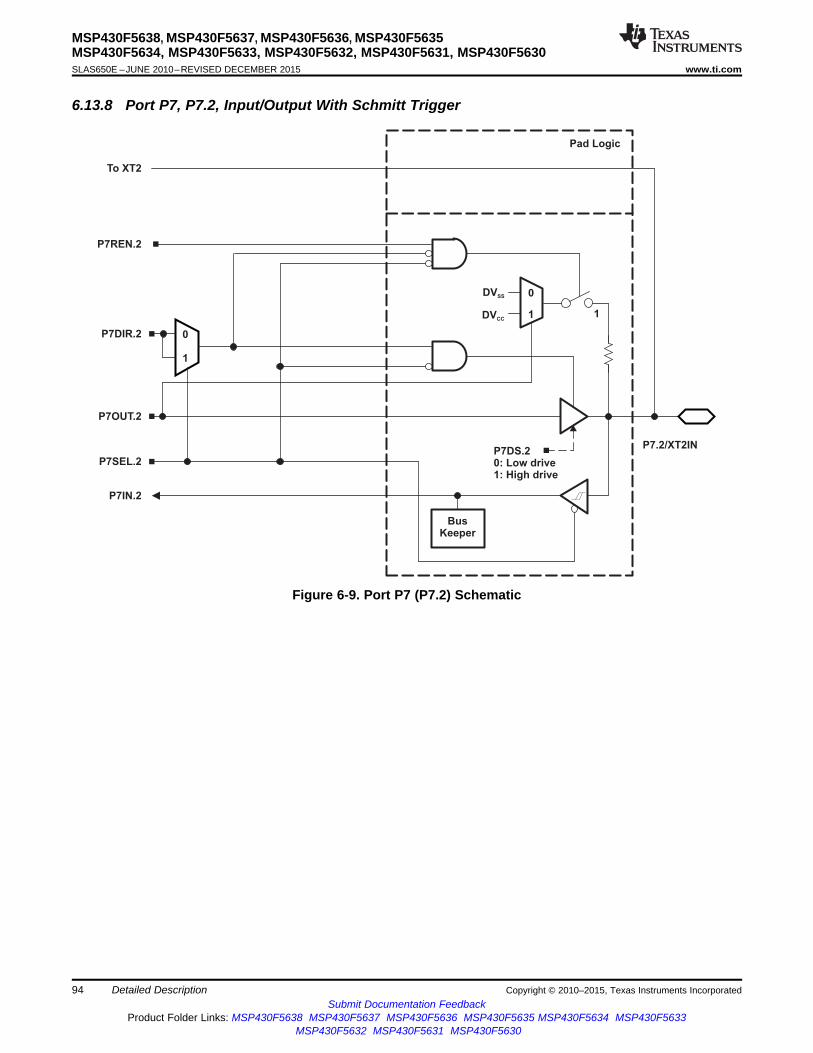
P7.2/XT2IN
P7SEL.2
1
0P7DIR.2
P7IN.2
P7OUT.2
1
0DVSS
DVCC
P7REN.2
Pad Logic
1
P7DS.20: Low drive1: High drive
BusKeeper
To XT2
MSP430F5638, MSP430F5637, MSP430F5636, MSP430F5635MSP430F5634, MSP430F5633, MSP430F5632, MSP430F5631, MSP430F5630SLAS650E –JUNE 2010–REVISED DECEMBER 2015 www.ti.com
6.13.8 Port P7, P7.2, Input/Output With Schmitt Trigger
Figure 6-9. Port P7 (P7.2) Schematic
94 Detailed Description Copyright © 2010–2015, Texas Instruments IncorporatedSubmit Documentation Feedback
Product Folder Links: MSP430F5638 MSP430F5637 MSP430F5636 MSP430F5635 MSP430F5634 MSP430F5633MSP430F5632 MSP430F5631 MSP430F5630

P7.3/XT2OUT
1
0P7DIR.3
P7IN.3
P7OUT.3
1
0DVSS
DVCC
P7REN.3
Pad Logic
1
P7DS.30: Low drive1: High drive
BusKeeper
To XT2
P7SEL.2
XT2BYPASS
P7SEL.3
MSP430F5638, MSP430F5637, MSP430F5636, MSP430F5635MSP430F5634, MSP430F5633, MSP430F5632, MSP430F5631, MSP430F5630
www.ti.com SLAS650E –JUNE 2010–REVISED DECEMBER 2015
6.13.9 Port P7, P7.3, Input/Output With Schmitt Trigger
Figure 6-10. Port P7 (P7.3) Schematic
Table 6-58. Port P7 (P7.2 and P7.3) Pin Functions
CONTROL BITS OR SIGNALS (1)PIN NAME (P5.x) x FUNCTION
P7DIR.x P7SEL.2 P7SEL.3 XT2BYPASSP7.2/XT2IN 2 P7.2 (I/O) I: 0; O: 1 0 X X
XT2IN crystal mode (2) X 1 X 0XT2IN bypass mode (2) X 1 X 1
P7.3/XT2OUT 3 P7.3 (I/O) I: 0; O: 1 0 0 XXT2OUT crystal mode (3) X 1 X 0P7.3 (I/O) (3) X 1 0 1
(1) X = Don't care(2) Setting P7SEL.2 causes the general-purpose I/O to be disabled. Pending the setting of XT2BYPASS, P7.2 is configured for crystal
mode or bypass mode.(3) Setting P7SEL.2 causes the general-purpose I/O to be disabled in crystal mode. When using bypass mode, P7.3 can be used as
general-purpose I/O.
Copyright © 2010–2015, Texas Instruments Incorporated Detailed Description 95Submit Documentation Feedback
Product Folder Links: MSP430F5638 MSP430F5637 MSP430F5636 MSP430F5635 MSP430F5634 MSP430F5633MSP430F5632 MSP430F5631 MSP430F5630
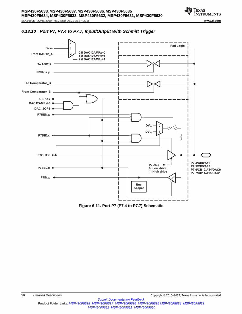
P7SEL.x
P7DIR.x
P7IN.x
P7OUT.x
1
0DVSS
DVCC
P7REN.x
Pad Logic
1
P7DS.x0: Low drive1: High drive
BusKeeper
From DAC12_A
P7.4/CB8/A12P7.5/CB9/A13P7.6/CB10/A14/DAC0P7.7/CB11/A15/DAC1
INCHx = y
To ADC12
To Comparator_B
From Comparator_B
CBPD.x
0
1
2
Dvss
0 if DAC12AMPx=01 if DAC12AMPx=12 if DAC12AMPx>1
DAC12AMPx>0
DAC12OPS
MSP430F5638, MSP430F5637, MSP430F5636, MSP430F5635MSP430F5634, MSP430F5633, MSP430F5632, MSP430F5631, MSP430F5630SLAS650E –JUNE 2010–REVISED DECEMBER 2015 www.ti.com
6.13.10 Port P7, P7.4 to P7.7, Input/Output With Schmitt Trigger
Figure 6-11. Port P7 (P7.4 to P7.7) Schematic
96 Detailed Description Copyright © 2010–2015, Texas Instruments IncorporatedSubmit Documentation Feedback
Product Folder Links: MSP430F5638 MSP430F5637 MSP430F5636 MSP430F5635 MSP430F5634 MSP430F5633MSP430F5632 MSP430F5631 MSP430F5630

MSP430F5638, MSP430F5637, MSP430F5636, MSP430F5635MSP430F5634, MSP430F5633, MSP430F5632, MSP430F5631, MSP430F5630
www.ti.com SLAS650E –JUNE 2010–REVISED DECEMBER 2015
Table 6-59. Port P7 (P7.4 to P7.7) Pin Functions
CONTROL BITS OR SIGNALS (1)PIN NAME (P7.x) x FUNCTION
P7DIR.x P7SEL.x CBPD.x DAC12OPS DAC12AMPxP7.4/CB8/A12 4 P7.4 (I/O) I: 0; O: 1 0 0 n/a n/a
Comparator_B input CB8 X X 1 n/a n/aA12 (2) (3) X 1 X n/a n/a
P7.5/CB9/A13 5 P7.5 (I/O) I: 0; O: 1 0 0 n/a n/aComparator_B input CB9 X X 1 n/a n/aA13 (2) (3) X 1 X n/a n/a
P7.6/CB10/A14/DAC0 6 P7.6 (I/O) I: 0; O: 1 0 0 X 0Comparator_B input CB10 X X 1 X 0A14 (2) (3) X 1 X X 0DAC12_A output DAC0 X X X 1 >1
P7.7/CB11/A15/DAC1 7 P7.7 (I/O) I: 0; O: 1 0 0 X 0Comparator_B input CB11 X X 1 X 0A15 (2) (3) X 1 X X 0DAC12_A output DAC1 X X X 1 >1
(1) X = Don't care(2) Setting the P7SEL.x bit disables the output driver and the input Schmitt trigger to prevent parasitic cross currents when applying analog
signals.(3) The ADC12_A channel Ax is connected internally to AVSS if not selected by the respective INCHx bits.
Copyright © 2010–2015, Texas Instruments Incorporated Detailed Description 97Submit Documentation Feedback
Product Folder Links: MSP430F5638 MSP430F5637 MSP430F5636 MSP430F5635 MSP430F5634 MSP430F5633MSP430F5632 MSP430F5631 MSP430F5630
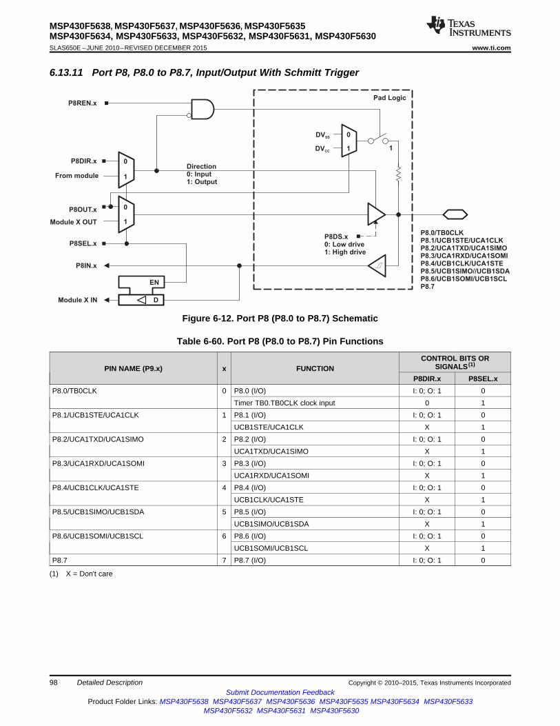
P8.0/TB0CLKP8.1/UCB1STE/UCA1CLKP8.2/UCA1TXD/UCA1SIMOP8.3/UCA1RXD/UCA1SOMIP8.4/UCB1CLK/UCA1STEP8.5/UCB1SIMO//UCB1SDAP8.6/UCB1SOMI/UCB1SCLP8.7
Direction0: Input1: Output
P8SEL.x
1
0P8DIR.x
P8IN.x
EN
Module X IN
1
0
Module X OUT
P8OUT.x
1
0DVSS
DVCC
P8REN.xPad Logic
1
P8DS.x0: Low drive1: High drive
D
From module
MSP430F5638, MSP430F5637, MSP430F5636, MSP430F5635MSP430F5634, MSP430F5633, MSP430F5632, MSP430F5631, MSP430F5630SLAS650E –JUNE 2010–REVISED DECEMBER 2015 www.ti.com
6.13.11 Port P8, P8.0 to P8.7, Input/Output With Schmitt Trigger
Figure 6-12. Port P8 (P8.0 to P8.7) Schematic
Table 6-60. Port P8 (P8.0 to P8.7) Pin Functions
CONTROL BITS ORSIGNALS (1)PIN NAME (P9.x) x FUNCTION
P8DIR.x P8SEL.xP8.0/TB0CLK 0 P8.0 (I/O) I: 0; O: 1 0
Timer TB0.TB0CLK clock input 0 1P8.1/UCB1STE/UCA1CLK 1 P8.1 (I/O) I: 0; O: 1 0
UCB1STE/UCA1CLK X 1P8.2/UCA1TXD/UCA1SIMO 2 P8.2 (I/O) I: 0; O: 1 0
UCA1TXD/UCA1SIMO X 1P8.3/UCA1RXD/UCA1SOMI 3 P8.3 (I/O) I: 0; O: 1 0
UCA1RXD/UCA1SOMI X 1P8.4/UCB1CLK/UCA1STE 4 P8.4 (I/O) I: 0; O: 1 0
UCB1CLK/UCA1STE X 1P8.5/UCB1SIMO/UCB1SDA 5 P8.5 (I/O) I: 0; O: 1 0
UCB1SIMO/UCB1SDA X 1P8.6/UCB1SOMI/UCB1SCL 6 P8.6 (I/O) I: 0; O: 1 0
UCB1SOMI/UCB1SCL X 1P8.7 7 P8.7 (I/O) I: 0; O: 1 0
(1) X = Don't care
98 Detailed Description Copyright © 2010–2015, Texas Instruments IncorporatedSubmit Documentation Feedback
Product Folder Links: MSP430F5638 MSP430F5637 MSP430F5636 MSP430F5635 MSP430F5634 MSP430F5633MSP430F5632 MSP430F5631 MSP430F5630
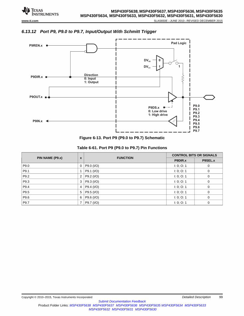
P9.0P9.1P9.2P9.3P9.4P9.5P9.6P9.7
Direction0: Input1: Output
P9DIR.x
P9IN.x
P9OUT.x
1
0DVSS
DVCC
P9REN.xPad Logic
1
P9DS.x0: Low drive1: High drive
MSP430F5638, MSP430F5637, MSP430F5636, MSP430F5635MSP430F5634, MSP430F5633, MSP430F5632, MSP430F5631, MSP430F5630
www.ti.com SLAS650E –JUNE 2010–REVISED DECEMBER 2015
6.13.12 Port P9, P9.0 to P9.7, Input/Output With Schmitt Trigger
Figure 6-13. Port P9 (P9.0 to P9.7) Schematic
Table 6-61. Port P9 (P9.0 to P9.7) Pin Functions
CONTROL BITS OR SIGNALSPIN NAME (P9.x) x FUNCTION
P9DIR.x P9SEL.xP9.0 0 P9.0 (I/O) I: 0; O: 1 0P9.1 1 P9.1 (I/O) I: 0; O: 1 0P9.2 2 P9.2 (I/O) I: 0; O: 1 0P9.3 3 P9.3 (I/O) I: 0; O: 1 0P9.4 4 P9.4 (I/O) I: 0; O: 1 0P9.5 5 P9.5 (I/O) I: 0; O: 1 0P9.6 6 P9.6 (I/O) I: 0; O: 1 0P9.7 7 P9.7 (I/O) I: 0; O: 1 0
Copyright © 2010–2015, Texas Instruments Incorporated Detailed Description 99Submit Documentation Feedback
Product Folder Links: MSP430F5638 MSP430F5637 MSP430F5636 MSP430F5635 MSP430F5634 MSP430F5633MSP430F5632 MSP430F5631 MSP430F5630
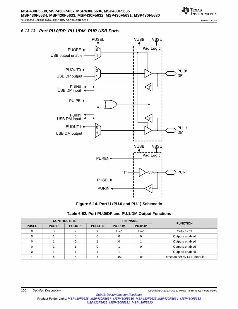
PUOPE 0
1
0
1
PUOUT0
PUSEL
Pad Logic
PU.0/
DP
VUSB VSSU
PU.1/
DM
0
1
PUOUT1
.PUIN1
USB DM input
PUIN0USB DP input
USB DM output
USB DP output
USB output enable
PUSEL
Pad Logic
PUR
VUSB VSSU
“1”
PUREN
PURIN
PUIPE
MSP430F5638, MSP430F5637, MSP430F5636, MSP430F5635MSP430F5634, MSP430F5633, MSP430F5632, MSP430F5631, MSP430F5630SLAS650E –JUNE 2010–REVISED DECEMBER 2015 www.ti.com
6.13.13 Port PU.0/DP, PU.1/DM, PUR USB Ports
Figure 6-14. Port U (PU.0 and PU.1) Schematic
Table 6-62. Port PU.0/DP and PU.1/DM Output Functions
CONTROL BITS PIN NAMEFUNCTION
PUSEL PUDIR PUOUT1 PUOUT0 PU.1/DM PU.0/DP0 0 X X Hi-Z Hi-Z Outputs off0 1 0 0 0 0 Outputs enabled0 1 0 1 0 1 Outputs enabled0 1 1 0 1 0 Outputs enabled0 1 1 1 1 1 Outputs enabled1 X X X DM DP Direction set by USB module
100 Detailed Description Copyright © 2010–2015, Texas Instruments IncorporatedSubmit Documentation Feedback
Product Folder Links: MSP430F5638 MSP430F5637 MSP430F5636 MSP430F5635 MSP430F5634 MSP430F5633MSP430F5632 MSP430F5631 MSP430F5630

MSP430F5638, MSP430F5637, MSP430F5636, MSP430F5635MSP430F5634, MSP430F5633, MSP430F5632, MSP430F5631, MSP430F5630
www.ti.com SLAS650E –JUNE 2010–REVISED DECEMBER 2015
Table 6-63. Port PUR Input Functions
CONTROL BITSFUNCTION
PUSEL PURENInput disabled0 0 Pullup disabledInput disabled0 1 Pullup enabledInput enabled1 0 Pullup disabledInput enabled1 1 Pullup enabled
Copyright © 2010–2015, Texas Instruments Incorporated Detailed Description 101Submit Documentation Feedback
Product Folder Links: MSP430F5638 MSP430F5637 MSP430F5636 MSP430F5635 MSP430F5634 MSP430F5633MSP430F5632 MSP430F5631 MSP430F5630

PJ.1/TDI/TCLKPJ.2/TMSPJ.3/TCK
From JTAG
1
0PJDIR.x
PJIN.x
EN
1
0
From JTAG
PJOUT.x
1
0DVSS
DVCC
PJREN.xPad Logic
1
PJDS.x0: Low drive1: High drive
D
DVSS
To JTAG
PJ.0/TDO
From JTAG
1
0PJDIR.0
PJIN.0
EN
1
0
From JTAG
PJOUT.0
1
0DVSS
DVCC
PJREN.0Pad Logic
1
PJDS.00: Low drive1: High drive
D
DVCC
MSP430F5638, MSP430F5637, MSP430F5636, MSP430F5635MSP430F5634, MSP430F5633, MSP430F5632, MSP430F5631, MSP430F5630SLAS650E –JUNE 2010–REVISED DECEMBER 2015 www.ti.com
6.13.14 Port J, J.0 JTAG Pin TDO, Input/Output With Schmitt Trigger or Output
Figure 6-15. Port J (PJ.0) Schematic
6.13.15 Port J, J.1 to J.3 JTAG Pins TMS, TCK, TDI/TCLK, Input/Output With SchmittTrigger or Output
Figure 6-16. Port PJ (PJ.1 to PJ.3) Schematic
102 Detailed Description Copyright © 2010–2015, Texas Instruments IncorporatedSubmit Documentation Feedback
Product Folder Links: MSP430F5638 MSP430F5637 MSP430F5636 MSP430F5635 MSP430F5634 MSP430F5633MSP430F5632 MSP430F5631 MSP430F5630

MSP430F5638, MSP430F5637, MSP430F5636, MSP430F5635MSP430F5634, MSP430F5633, MSP430F5632, MSP430F5631, MSP430F5630
www.ti.com SLAS650E –JUNE 2010–REVISED DECEMBER 2015
Table 6-64. Port PJ (PJ.0 to PJ.3) Pin Functions
CONTROL BITS ORSIGNALS (1)PIN NAME (PJ.x) x FUNCTION
PJDIR.xPJ.0/TDO 0 PJ.0 (I/O) (2) I: 0; O: 1
TDO (3) XPJ.1/TDI/TCLK 1 PJ.1 (I/O) (2) I: 0; O: 1
TDI/TCLK (3) (4) XPJ.2/TMS 2 PJ.2 (I/O) (2) I: 0; O: 1
TMS (3) (4) XPJ.3/TCK 3 PJ.3 (I/O) (2) I: 0; O: 1
TCK (3) (4) X
(1) X = Don't care(2) Default condition(3) The pin direction is controlled by the JTAG module.(4) In JTAG mode, pullups are activated automatically on TMS, TCK, and TDI/TCLK. PJREN.x are don't care.
Copyright © 2010–2015, Texas Instruments Incorporated Detailed Description 103Submit Documentation Feedback
Product Folder Links: MSP430F5638 MSP430F5637 MSP430F5636 MSP430F5635 MSP430F5634 MSP430F5633MSP430F5632 MSP430F5631 MSP430F5630

MSP430F5638, MSP430F5637, MSP430F5636, MSP430F5635MSP430F5634, MSP430F5633, MSP430F5632, MSP430F5631, MSP430F5630SLAS650E –JUNE 2010–REVISED DECEMBER 2015 www.ti.com
6.14 Device DescriptorsTable 6-65 list the complete contents of the device descriptor tag-length-value (TLV) structure for eachdevice type.
Table 6-65. MSP430F563x Device Descriptor Table (1)
VALUESIZEDESCRIPTION ADDRESS (bytes) F5638 F5637 F5636 F5635 F5634 F5633 F5632 F5631 F5630
Info length 01A00h 1 06h 06h 06h 06h 06h 06h 06h 06h 06h
CRC length 01A01h 1 06h 06h 06h 06h 06h 06h 06h 06h 06h
CRC value 01A02h 2 per unit per unit per unit per unit per unit per unit per unit per unit per unitInfo Block
Device ID 01A04h 2 8014h 8012h 8010h 800Eh 8044h 8042h 8040h 803Eh 803Ch
Hardware revision 01A06h 1 per unit per unit per unit per unit per unit per unit per unit per unit per unit
Firmware revision 01A07h 1 per unit per unit per unit per unit per unit per unit per unit per unit per unit
Die record tag 01A08h 1 08h 08h 08h 08h 08h 08h 08h 08h 08h
Die record length 01A09h 1 0Ah 0Ah 0Ah 0Ah 0Ah 0Ah 0Ah 0Ah 0Ah
Lot/wafer ID 01A0Ah 4 per unit per unit per unit per unit per unit per unit per unit per unit per unitDie Record
Die X position 01A0Eh 2 per unit per unit per unit per unit per unit per unit per unit per unit per unit
Die Y position 01A10h 2 per unit per unit per unit per unit per unit per unit per unit per unit per unit
Test results 01A12h 2 per unit per unit per unit per unit per unit per unit per unit per unit per unit
ADC12 calibration tag 01A14h 1 11h 11h 11h 11h 11h 11h 11h 11h 11h
ADC12 calibration length 01A15h 1 10h 10h 10h 10h 10h 10h 10h 10h 10h
ADC gain factor 01A16h 2 per unit per unit per unit per unit per unit per unit per unit per unit per unit
ADC offset 01A18h 2 per unit per unit per unit per unit per unit per unit per unit per unit per unit
ADC 1.5-V reference 01A1Ah 2 per unit per unit per unit per unit per unit per unit per unit per unit per unittemp. l 30°C
ADC 1.5-V reference 01A1Ch 2 per unit per unit per unit per unit per unit per unit per unit per unit per unitADC12 temp. sensor 85°CCalibration
ADC 2.0-V reference 01A1Eh 2 per unit per unit per unit per unit per unit per unit per unit per unit per unittemp. sensor 30°C
ADC 2.0-V reference 01A20h 2 per unit per unit per unit per unit per unit per unit per unit per unit per unittemp. sensor 85°C
ADC 2.5-V reference 01A22h 2 per unit per unit per unit per unit per unit per unit per unit per unit per unittemp. sensor 30°C
ADC 2.5-V reference 01A24h 2 per unit per unit per unit per unit per unit per unit per unit per unit per unittemp. sensor 85°C
(1) NA = Not applicable
104 Detailed Description Copyright © 2010–2015, Texas Instruments IncorporatedSubmit Documentation Feedback
Product Folder Links: MSP430F5638 MSP430F5637 MSP430F5636 MSP430F5635 MSP430F5634 MSP430F5633MSP430F5632 MSP430F5631 MSP430F5630

MSP430F5638, MSP430F5637, MSP430F5636, MSP430F5635MSP430F5634, MSP430F5633, MSP430F5632, MSP430F5631, MSP430F5630
www.ti.com SLAS650E –JUNE 2010–REVISED DECEMBER 2015
7 Device and Documentation Support
7.1 Device Support
7.1.1 Development Support
7.1.1.1 Getting Started and Next Steps
For more information on the MSP430™ family of devices and the tools and libraries that are available tohelp with your development, visit the Getting Started page.
7.1.1.2 Development Tools Support
All MSP430™ microcontrollers are supported by a wide variety of software and hardware developmenttools. Tools are available from TI and various third parties. See them all at www.ti.com/msp430tools.
7.1.1.2.1 Hardware Features
See the Code Composer Studio for MSP430 User's Guide (SLAU157) for details on the available features.BREAK- RANGE LPMx.5MSP430 4-WIRE 2-WIRE CLOCK STATE TRACEPOINTS BREAK- DEBUGGINGARCHITECTURE JTAG JTAG CONTROL SEQUENCER BUFFER(N) POINTS SUPPORT
MSP430Xv2 Yes Yes 8 Yes Yes Yes Yes No
7.1.1.2.2 Recommended Hardware Options
7.1.1.2.2.1 Target Socket Boards
The target socket boards allow easy programming and debugging of the device using JTAG. They alsofeature header pin outs for prototyping. Target socket boards are orderable individually or as a kit with theJTAG programmer and debugger included. The following table shows the compatible target boards andthe supported packages.
PACKAGE TARGET BOARD AND PROGRAMMER BUNDLE TARGET BOARD ONLY100-pin LQFP (PZ) MSP-FET430U100USB MSP-TS430PZ100USB
7.1.1.2.2.2 Experimenter Boards
Experimenter Boards and Evaluation kits are available for some MSP430 devices. These kits featureadditional hardware components and connectivity for full system evaluation and prototyping. Seewww.ti.com/msp430tools for details.
7.1.1.2.2.3 Debugging and Programming Tools
Hardware programming and debugging tools are available from TI and from its third party suppliers. Seethe full list of available tools at www.ti.com/msp430tools.
7.1.1.2.2.4 Production Programmers
The production programmers expedite loading firmware to devices by programming several devicessimultaneously.
PART NUMBER PC PORT FEATURES PROVIDERProgram up to eight devices at a time. Works with a PC or as aMSP-GANG Serial and USB Texas Instrumentsstand-alone package.
Copyright © 2010–2015, Texas Instruments Incorporated Device and Documentation Support 105Submit Documentation Feedback
Product Folder Links: MSP430F5638 MSP430F5637 MSP430F5636 MSP430F5635 MSP430F5634 MSP430F5633MSP430F5632 MSP430F5631 MSP430F5630

MSP430F5638, MSP430F5637, MSP430F5636, MSP430F5635MSP430F5634, MSP430F5633, MSP430F5632, MSP430F5631, MSP430F5630SLAS650E –JUNE 2010–REVISED DECEMBER 2015 www.ti.com
7.1.1.2.3 Recommended Software Options
7.1.1.2.3.1 Integrated Development Environments
Software development tools are available from TI or from third parties. Open source solutions are alsoavailable.
This device is supported by Code Composer Studio™ IDE (CCS).
7.1.1.2.3.2 MSP430Ware
MSP430Ware is a collection of code examples, data sheets, and other design resources for all MSP430devices delivered in a convenient package. In addition to providing a complete collection of existingMSP430 design resources, MSP430Ware also includes a high-level API called MSP430 Driver Library.This library makes it easy to program MSP430 hardware. MSP430Ware is available as a component ofCCS or as a stand-alone package.
7.1.1.2.3.3 TI-RTOS
TI-RTOS is a complete real-time operating system for the MSP430 microcontrollers. It combines a real-time multitasking kernel SYS/BIOS with additional middleware components. TI-RTOS is available free ofcharge and provided with full source code.
7.1.1.2.3.4 MSP430 USB Developer's Package
MSP430 USB Developer's Package is an easy-to-use USB stack implementation for the MSP430microcontrollers.
7.1.1.2.3.5 Command-Line Programmer
MSP430 Flasher is an open-source, shell-based interface for programming MSP430 microcontrollersthrough a FET programmer or eZ430 using JTAG or Spy-Bi-Wire (SBW) communication. MSP430 Flashercan be used to download binary files (.txt or .hex) files directly to the MSP430 Flash without the need foran IDE.
7.1.2 Device and Development Tool NomenclatureTo designate the stages in the product development cycle, TI assigns prefixes to the part numbers of allMSP430 MCU devices and support tools. Each MSP430 MCU commercial family member has one ofthree prefixes: MSP, PMS, or XMS (for example, MSP430F5438A). TI recommends two of three possibleprefix designators for its support tools: MSP and MSPX. These prefixes represent evolutionary stages ofproduct development from engineering prototypes (with XMS for devices and MSPX for tools) through fullyqualified production devices and tools (with MSP for devices and MSP for tools).
Device development evolutionary flow:
XMS – Experimental device that is not necessarily representative of the electrical specifications for thefinal device
PMS – Final silicon die that conforms to the electrical specifications for the device but has not completedquality and reliability verification
MSP – Fully qualified production device
Support tool development evolutionary flow:
MSPX – Development-support product that has not yet completed TI's internal qualification testing.
MSP – Fully-qualified development-support product
XMS and PMS devices and MSPX development-support tools are shipped against the followingdisclaimer:
"Developmental product is intended for internal evaluation purposes."106 Device and Documentation Support Copyright © 2010–2015, Texas Instruments Incorporated
Submit Documentation FeedbackProduct Folder Links: MSP430F5638 MSP430F5637 MSP430F5636 MSP430F5635 MSP430F5634 MSP430F5633
MSP430F5632 MSP430F5631 MSP430F5630

Processor Family CC = Embedded RF RadioMSP = Mixed-Signal ProcessorXMS = Experimental SiliconPMS = Prototype Device
MCU Platform 430 = MSP430 low-power microcontroller platform
Device Type Memory TypeC = ROMF = FlashFR = FRAMG = Flash or FRAM (Value Line)L = No Nonvolatile Memory
Specialized ApplicationAFE = Analog Front EndBT = Preprogrammed withBQ = Contactless PowerCG = ROM MedicalFE = Flash Energy MeterFG = Flash MedicalFW = Flash Electronic Flow Meter
Bluetooth
Series 1 Series = Up to 8 MHz2 Series = Up to 16 MHz3 Series = Legacy4 Series = Up to 16 MHz with LCD
5 Series = Up to 25 MHz6 Series = Up to 25 MHz with LCD0 = Low-Voltage Series
Feature Set Various Levels of Integration Within a Series
Optional: A = Revision N/A
Optional: Temperature Range S = 0°C to 50 CC to 70 C
I = 40 C to 85 CT = –40 C to 105 C
°C = 0° °
– ° °° °
Packaging http://www.ti.com/packaging
Optional: Tape and Reel T = Small ReelR = Large ReelNo Markings = Tube or Tray
Optional: Additional Features -EP = Enhanced Product ( 40°C to 105°C)-HT = Extreme Temperature Parts ( 55°C to 150°C)-Q1 = Automotive Q100 Qualified
––
MSP 430 F 5 438 A I ZQW T -EP
Processor Family
Series Optional: Temperature Range
MCU Platform
PackagingDevice Type
Optional: A = Revision
Optional: Tape and Reel
Feature Set
Optional: Additional Features
MSP430F5638, MSP430F5637, MSP430F5636, MSP430F5635MSP430F5634, MSP430F5633, MSP430F5632, MSP430F5631, MSP430F5630
www.ti.com SLAS650E –JUNE 2010–REVISED DECEMBER 2015
MSP devices and MSP development-support tools have been characterized fully, and the quality andreliability of the device have been demonstrated fully. TI's standard warranty applies.
Predictions show that prototype devices (XMS and PMS) have a greater failure rate than the standardproduction devices. TI recommends that these devices not be used in any production system becausetheir expected end-use failure rate still is undefined. Only qualified production devices are to be used.
TI device nomenclature also includes a suffix with the device family name. This suffix indicates thepackage type (for example, PZP) and temperature range (for example, T). Figure 7-1 provides a legendfor reading the complete device name for any family member.
Figure 7-1. Device Nomenclature
Copyright © 2010–2015, Texas Instruments Incorporated Device and Documentation Support 107Submit Documentation Feedback
Product Folder Links: MSP430F5638 MSP430F5637 MSP430F5636 MSP430F5635 MSP430F5634 MSP430F5633MSP430F5632 MSP430F5631 MSP430F5630
MSP430F5638, MSP430F5637, MSP430F5636, MSP430F5635MSP430F5634, MSP430F5633, MSP430F5632, MSP430F5631, MSP430F5630SLAS650E –JUNE 2010–REVISED DECEMBER 2015 www.ti.com
7.2 Documentation SupportThe following documents describe the devices. Copies of these documents are available on the Internet atwww.ti.com.
SLAU208 MSP430x5xx and MSP430x6xx Family User's Guide. Detailed information on the modulesand peripherals available in this device family.
SLAZ323 MSP430F5638 Device Erratasheet. Describes the known exceptions to the functionalspecifications for this device.
SLAZ322 MSP430F5637 Device Erratasheet. Describes the known exceptions to the functionalspecifications for this device.
SLAZ321 MSP430F5636 Device Erratasheet. Describes the known exceptions to the functionalspecifications for this device.
SLAZ320 MSP430F5635 Device Erratasheet. Describes the known exceptions to the functionalspecifications for this device.
SLAZ319 MSP430F5634 Device Erratasheet. Describes the known exceptions to the functionalspecifications for this device.
SLAZ318 MSP430F5633 Device Erratasheet. Describes the known exceptions to the functionalspecifications for this device.
SLAZ317 MSP430F5632 Device Erratasheet. Describes the known exceptions to the functionalspecifications for this device.
SLAZ316 MSP430F5631 Device Erratasheet. Describes the known exceptions to the functionalspecifications for this device.
SLAZ315 MSP430F5630 Device Erratasheet. Describes the known exceptions to the functionalspecifications for this device.
7.3 Related LinksTable 7-1 lists quick access links. Categories include technical documents, support and communityresources, tools and software, and quick access to sample or buy.
Table 7-1. Related Links
TECHNICAL TOOLS & SUPPORT &PARTS PRODUCT FOLDER SAMPLE & BUY DOCUMENTS SOFTWARE COMMUNITYMSP430F5638 Click here Click here Click here Click here Click hereMSP430F5637 Click here Click here Click here Click here Click hereMSP430F5636 Click here Click here Click here Click here Click hereMSP430F5635 Click here Click here Click here Click here Click hereMSP430F5634 Click here Click here Click here Click here Click hereMSP430F5633 Click here Click here Click here Click here Click hereMSP430F5632 Click here Click here Click here Click here Click hereMSP430F5631 Click here Click here Click here Click here Click hereMSP430F5630 Click here Click here Click here Click here Click here
108 Device and Documentation Support Copyright © 2010–2015, Texas Instruments IncorporatedSubmit Documentation Feedback
Product Folder Links: MSP430F5638 MSP430F5637 MSP430F5636 MSP430F5635 MSP430F5634 MSP430F5633MSP430F5632 MSP430F5631 MSP430F5630
MSP430F5638, MSP430F5637, MSP430F5636, MSP430F5635MSP430F5634, MSP430F5633, MSP430F5632, MSP430F5631, MSP430F5630
www.ti.com SLAS650E –JUNE 2010–REVISED DECEMBER 2015
7.4 Community ResourcesThe following links connect to TI community resources. Linked contents are provided "AS IS" by therespective contributors. They do not constitute TI specifications and do not necessarily reflect TI's views;see TI's Terms of Use.
TI E2E™ CommunityTI's Engineer-to-Engineer (E2E) Community. Created to foster collaboration among engineers. Ate2e.ti.com, you can ask questions, share knowledge, explore ideas, and help solve problems with fellowengineers.
TI Embedded Processors WikiTexas Instruments Embedded Processors Wiki. Established to help developers get started with embeddedprocessors from Texas Instruments and to foster innovation and growth of general knowledge about thehardware and software surrounding these devices.
7.5 TrademarksMSP430, Code Composer Studio, E2E are trademarks of Texas Instruments.All other trademarks are the property of their respective owners.
7.6 Electrostatic Discharge CautionThis integrated circuit can be damaged by ESD. Texas Instruments recommends that all integrated circuits be handled withappropriate precautions. Failure to observe proper handling and installation procedures can cause damage.
ESD damage can range from subtle performance degradation to complete device failure. Precision integrated circuits may be moresusceptible to damage because very small parametric changes could cause the device not to meet its published specifications.
7.7 Export Control NoticeRecipient agrees to not knowingly export or re-export, directly or indirectly, any product or technical data(as defined by the U.S., EU, and other Export Administration Regulations) including software, or anycontrolled product restricted by other applicable national regulations, received from disclosing party undernondisclosure obligations (if any), or any direct product of such technology, to any destination to whichsuch export or re-export is restricted or prohibited by U.S. or other applicable laws, without obtaining priorauthorization from U.S. Department of Commerce and other competent Government authorities to theextent required by those laws.
7.8 GlossaryTI Glossary This glossary lists and explains terms, acronyms, and definitions.
8 Mechanical, Packaging, and Orderable Information
The following pages include mechanical, packaging, and orderable information. This information is themost current data available for the designated devices. This data is subject to change without notice andrevision of this document. For browser-based versions of this data sheet, refer to the left-hand navigation.
Copyright © 2010–2015, Texas Instruments Incorporated Mechanical, Packaging, and Orderable Information 109Submit Documentation Feedback
Product Folder Links: MSP430F5638 MSP430F5637 MSP430F5636 MSP430F5635 MSP430F5634 MSP430F5633MSP430F5632 MSP430F5631 MSP430F5630
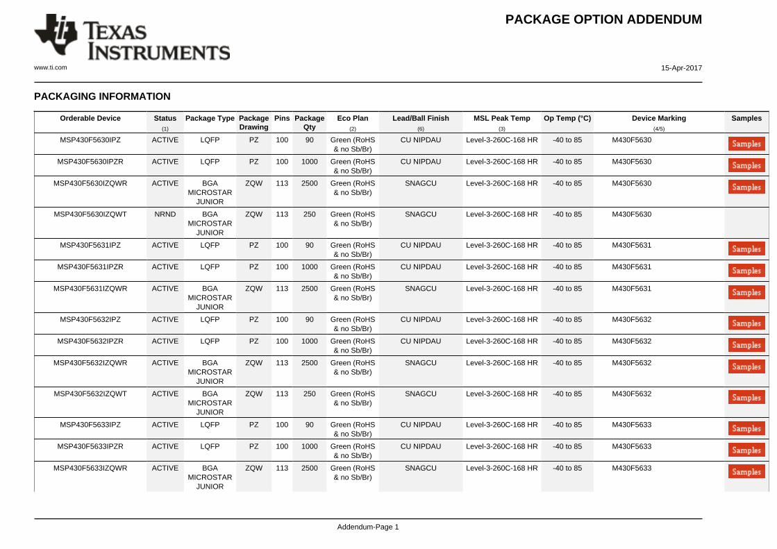
PACKAGE OPTION ADDENDUM
www.ti.com 15-Apr-2017
Addendum-Page 1
PACKAGING INFORMATION
Orderable Device Status(1)
Package Type PackageDrawing
Pins PackageQty
Eco Plan(2)
Lead/Ball Finish(6)
MSL Peak Temp(3)
Op Temp (°C) Device Marking(4/5)
Samples
MSP430F5630IPZ ACTIVE LQFP PZ 100 90 Green (RoHS& no Sb/Br)
CU NIPDAU Level-3-260C-168 HR -40 to 85 M430F5630
MSP430F5630IPZR ACTIVE LQFP PZ 100 1000 Green (RoHS& no Sb/Br)
CU NIPDAU Level-3-260C-168 HR -40 to 85 M430F5630
MSP430F5630IZQWR ACTIVE BGAMICROSTAR
JUNIOR
ZQW 113 2500 Green (RoHS& no Sb/Br)
SNAGCU Level-3-260C-168 HR -40 to 85 M430F5630
MSP430F5630IZQWT NRND BGAMICROSTAR
JUNIOR
ZQW 113 250 Green (RoHS& no Sb/Br)
SNAGCU Level-3-260C-168 HR -40 to 85 M430F5630
MSP430F5631IPZ ACTIVE LQFP PZ 100 90 Green (RoHS& no Sb/Br)
CU NIPDAU Level-3-260C-168 HR -40 to 85 M430F5631
MSP430F5631IPZR ACTIVE LQFP PZ 100 1000 Green (RoHS& no Sb/Br)
CU NIPDAU Level-3-260C-168 HR -40 to 85 M430F5631
MSP430F5631IZQWR ACTIVE BGAMICROSTAR
JUNIOR
ZQW 113 2500 Green (RoHS& no Sb/Br)
SNAGCU Level-3-260C-168 HR -40 to 85 M430F5631
MSP430F5632IPZ ACTIVE LQFP PZ 100 90 Green (RoHS& no Sb/Br)
CU NIPDAU Level-3-260C-168 HR -40 to 85 M430F5632
MSP430F5632IPZR ACTIVE LQFP PZ 100 1000 Green (RoHS& no Sb/Br)
CU NIPDAU Level-3-260C-168 HR -40 to 85 M430F5632
MSP430F5632IZQWR ACTIVE BGAMICROSTAR
JUNIOR
ZQW 113 2500 Green (RoHS& no Sb/Br)
SNAGCU Level-3-260C-168 HR -40 to 85 M430F5632
MSP430F5632IZQWT ACTIVE BGAMICROSTAR
JUNIOR
ZQW 113 250 Green (RoHS& no Sb/Br)
SNAGCU Level-3-260C-168 HR -40 to 85 M430F5632
MSP430F5633IPZ ACTIVE LQFP PZ 100 90 Green (RoHS& no Sb/Br)
CU NIPDAU Level-3-260C-168 HR -40 to 85 M430F5633
MSP430F5633IPZR ACTIVE LQFP PZ 100 1000 Green (RoHS& no Sb/Br)
CU NIPDAU Level-3-260C-168 HR -40 to 85 M430F5633
MSP430F5633IZQWR ACTIVE BGAMICROSTAR
JUNIOR
ZQW 113 2500 Green (RoHS& no Sb/Br)
SNAGCU Level-3-260C-168 HR -40 to 85 M430F5633
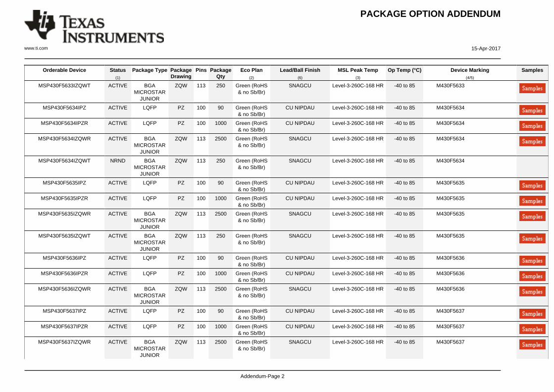
PACKAGE OPTION ADDENDUM
www.ti.com 15-Apr-2017
Addendum-Page 2
Orderable Device Status(1)
Package Type PackageDrawing
Pins PackageQty
Eco Plan(2)
Lead/Ball Finish(6)
MSL Peak Temp(3)
Op Temp (°C) Device Marking(4/5)
Samples
MSP430F5633IZQWT ACTIVE BGAMICROSTAR
JUNIOR
ZQW 113 250 Green (RoHS& no Sb/Br)
SNAGCU Level-3-260C-168 HR -40 to 85 M430F5633
MSP430F5634IPZ ACTIVE LQFP PZ 100 90 Green (RoHS& no Sb/Br)
CU NIPDAU Level-3-260C-168 HR -40 to 85 M430F5634
MSP430F5634IPZR ACTIVE LQFP PZ 100 1000 Green (RoHS& no Sb/Br)
CU NIPDAU Level-3-260C-168 HR -40 to 85 M430F5634
MSP430F5634IZQWR ACTIVE BGAMICROSTAR
JUNIOR
ZQW 113 2500 Green (RoHS& no Sb/Br)
SNAGCU Level-3-260C-168 HR -40 to 85 M430F5634
MSP430F5634IZQWT NRND BGAMICROSTAR
JUNIOR
ZQW 113 250 Green (RoHS& no Sb/Br)
SNAGCU Level-3-260C-168 HR -40 to 85 M430F5634
MSP430F5635IPZ ACTIVE LQFP PZ 100 90 Green (RoHS& no Sb/Br)
CU NIPDAU Level-3-260C-168 HR -40 to 85 M430F5635
MSP430F5635IPZR ACTIVE LQFP PZ 100 1000 Green (RoHS& no Sb/Br)
CU NIPDAU Level-3-260C-168 HR -40 to 85 M430F5635
MSP430F5635IZQWR ACTIVE BGAMICROSTAR
JUNIOR
ZQW 113 2500 Green (RoHS& no Sb/Br)
SNAGCU Level-3-260C-168 HR -40 to 85 M430F5635
MSP430F5635IZQWT ACTIVE BGAMICROSTAR
JUNIOR
ZQW 113 250 Green (RoHS& no Sb/Br)
SNAGCU Level-3-260C-168 HR -40 to 85 M430F5635
MSP430F5636IPZ ACTIVE LQFP PZ 100 90 Green (RoHS& no Sb/Br)
CU NIPDAU Level-3-260C-168 HR -40 to 85 M430F5636
MSP430F5636IPZR ACTIVE LQFP PZ 100 1000 Green (RoHS& no Sb/Br)
CU NIPDAU Level-3-260C-168 HR -40 to 85 M430F5636
MSP430F5636IZQWR ACTIVE BGAMICROSTAR
JUNIOR
ZQW 113 2500 Green (RoHS& no Sb/Br)
SNAGCU Level-3-260C-168 HR -40 to 85 M430F5636
MSP430F5637IPZ ACTIVE LQFP PZ 100 90 Green (RoHS& no Sb/Br)
CU NIPDAU Level-3-260C-168 HR -40 to 85 M430F5637
MSP430F5637IPZR ACTIVE LQFP PZ 100 1000 Green (RoHS& no Sb/Br)
CU NIPDAU Level-3-260C-168 HR -40 to 85 M430F5637
MSP430F5637IZQWR ACTIVE BGAMICROSTAR
JUNIOR
ZQW 113 2500 Green (RoHS& no Sb/Br)
SNAGCU Level-3-260C-168 HR -40 to 85 M430F5637

PACKAGE OPTION ADDENDUM
www.ti.com 15-Apr-2017
Addendum-Page 3
Orderable Device Status(1)
Package Type PackageDrawing
Pins PackageQty
Eco Plan(2)
Lead/Ball Finish(6)
MSL Peak Temp(3)
Op Temp (°C) Device Marking(4/5)
Samples
MSP430F5638IPZ ACTIVE LQFP PZ 100 90 Green (RoHS& no Sb/Br)
CU NIPDAU Level-3-260C-168 HR -40 to 85 M430F5638
MSP430F5638IPZR ACTIVE LQFP PZ 100 1000 Green (RoHS& no Sb/Br)
CU NIPDAU Level-3-260C-168 HR -40 to 85 M430F5638
MSP430F5638IZQWR ACTIVE BGAMICROSTAR
JUNIOR
ZQW 113 2500 Green (RoHS& no Sb/Br)
SNAGCU Level-3-260C-168 HR -40 to 85 M430F5638
MSP430F5638IZQWT ACTIVE BGAMICROSTAR
JUNIOR
ZQW 113 250 Green (RoHS& no Sb/Br)
SNAGCU Level-3-260C-168 HR -40 to 85 M430F5638
(1) The marketing status values are defined as follows:ACTIVE: Product device recommended for new designs.LIFEBUY: TI has announced that the device will be discontinued, and a lifetime-buy period is in effect.NRND: Not recommended for new designs. Device is in production to support existing customers, but TI does not recommend using this part in a new design.PREVIEW: Device has been announced but is not in production. Samples may or may not be available.OBSOLETE: TI has discontinued the production of the device.
(2) Eco Plan - The planned eco-friendly classification: Pb-Free (RoHS), Pb-Free (RoHS Exempt), or Green (RoHS & no Sb/Br) - please check http://www.ti.com/productcontent for the latest availabilityinformation and additional product content details.TBD: The Pb-Free/Green conversion plan has not been defined.Pb-Free (RoHS): TI's terms "Lead-Free" or "Pb-Free" mean semiconductor products that are compatible with the current RoHS requirements for all 6 substances, including the requirement thatlead not exceed 0.1% by weight in homogeneous materials. Where designed to be soldered at high temperatures, TI Pb-Free products are suitable for use in specified lead-free processes.Pb-Free (RoHS Exempt): This component has a RoHS exemption for either 1) lead-based flip-chip solder bumps used between the die and package, or 2) lead-based die adhesive used betweenthe die and leadframe. The component is otherwise considered Pb-Free (RoHS compatible) as defined above.Green (RoHS & no Sb/Br): TI defines "Green" to mean Pb-Free (RoHS compatible), and free of Bromine (Br) and Antimony (Sb) based flame retardants (Br or Sb do not exceed 0.1% by weightin homogeneous material)
(3) MSL, Peak Temp. - The Moisture Sensitivity Level rating according to the JEDEC industry standard classifications, and peak solder temperature.
(4) There may be additional marking, which relates to the logo, the lot trace code information, or the environmental category on the device.
(5) Multiple Device Markings will be inside parentheses. Only one Device Marking contained in parentheses and separated by a "~" will appear on a device. If a line is indented then it is a continuationof the previous line and the two combined represent the entire Device Marking for that device.
(6) Lead/Ball Finish - Orderable Devices may have multiple material finish options. Finish options are separated by a vertical ruled line. Lead/Ball Finish values may wrap to two lines if the finishvalue exceeds the maximum column width.
PACKAGE OPTION ADDENDUM
www.ti.com 15-Apr-2017
Addendum-Page 4
Important Information and Disclaimer:The information provided on this page represents TI's knowledge and belief as of the date that it is provided. TI bases its knowledge and belief on informationprovided by third parties, and makes no representation or warranty as to the accuracy of such information. Efforts are underway to better integrate information from third parties. TI has taken andcontinues to take reasonable steps to provide representative and accurate information but may not have conducted destructive testing or chemical analysis on incoming materials and chemicals.TI and TI suppliers consider certain information to be proprietary, and thus CAS numbers and other limited information may not be available for release.
In no event shall TI's liability arising out of such information exceed the total purchase price of the TI part(s) at issue in this document sold by TI to Customer on an annual basis.
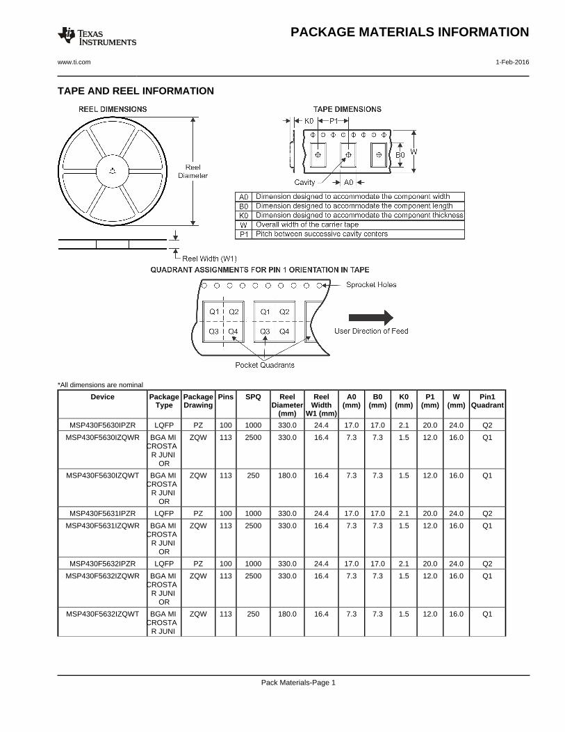
TAPE AND REEL INFORMATION
*All dimensions are nominal
Device PackageType
PackageDrawing
Pins SPQ ReelDiameter
(mm)
ReelWidth
W1 (mm)
A0(mm)
B0(mm)
K0(mm)
P1(mm)
W(mm)
Pin1Quadrant
MSP430F5630IPZR LQFP PZ 100 1000 330.0 24.4 17.0 17.0 2.1 20.0 24.0 Q2
MSP430F5630IZQWR BGA MI CROSTA
R JUNI OR
ZQW 113 2500 330.0 16.4 7.3 7.3 1.5 12.0 16.0 Q1
MSP430F5630IZQWT BGA MI CROSTA
R JUNI OR
ZQW 113 250 180.0 16.4 7.3 7.3 1.5 12.0 16.0 Q1
MSP430F5631IPZR LQFP PZ 100 1000 330.0 24.4 17.0 17.0 2.1 20.0 24.0 Q2
MSP430F5631IZQWR BGA MI CROSTA
R JUNI OR
ZQW 113 2500 330.0 16.4 7.3 7.3 1.5 12.0 16.0 Q1
MSP430F5632IPZR LQFP PZ 100 1000 330.0 24.4 17.0 17.0 2.1 20.0 24.0 Q2
MSP430F5632IZQWR BGA MI CROSTA
R JUNI OR
ZQW 113 2500 330.0 16.4 7.3 7.3 1.5 12.0 16.0 Q1
MSP430F5632IZQWT BGA MI CROSTA
R JUNI
ZQW 113 250 180.0 16.4 7.3 7.3 1.5 12.0 16.0 Q1
PACKAGE MATERIALS INFORMATION
www.ti.com 1-Feb-2016
Pack Materials-Page 1
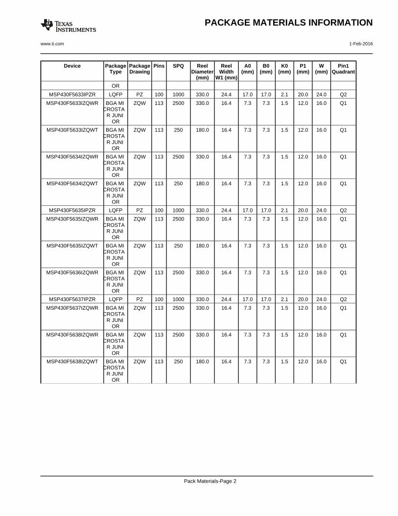
Device PackageType
PackageDrawing
Pins SPQ ReelDiameter
(mm)
ReelWidth
W1 (mm)
A0(mm)
B0(mm)
K0(mm)
P1(mm)
W(mm)
Pin1Quadrant
OR
MSP430F5633IPZR LQFP PZ 100 1000 330.0 24.4 17.0 17.0 2.1 20.0 24.0 Q2
MSP430F5633IZQWR BGA MI CROSTA
R JUNI OR
ZQW 113 2500 330.0 16.4 7.3 7.3 1.5 12.0 16.0 Q1
MSP430F5633IZQWT BGA MI CROSTA
R JUNI OR
ZQW 113 250 180.0 16.4 7.3 7.3 1.5 12.0 16.0 Q1
MSP430F5634IZQWR BGA MI CROSTA
R JUNI OR
ZQW 113 2500 330.0 16.4 7.3 7.3 1.5 12.0 16.0 Q1
MSP430F5634IZQWT BGA MI CROSTA
R JUNI OR
ZQW 113 250 180.0 16.4 7.3 7.3 1.5 12.0 16.0 Q1
MSP430F5635IPZR LQFP PZ 100 1000 330.0 24.4 17.0 17.0 2.1 20.0 24.0 Q2
MSP430F5635IZQWR BGA MI CROSTA
R JUNI OR
ZQW 113 2500 330.0 16.4 7.3 7.3 1.5 12.0 16.0 Q1
MSP430F5635IZQWT BGA MI CROSTA
R JUNI OR
ZQW 113 250 180.0 16.4 7.3 7.3 1.5 12.0 16.0 Q1
MSP430F5636IZQWR BGA MI CROSTA
R JUNI OR
ZQW 113 2500 330.0 16.4 7.3 7.3 1.5 12.0 16.0 Q1
MSP430F5637IPZR LQFP PZ 100 1000 330.0 24.4 17.0 17.0 2.1 20.0 24.0 Q2
MSP430F5637IZQWR BGA MI CROSTA
R JUNI OR
ZQW 113 2500 330.0 16.4 7.3 7.3 1.5 12.0 16.0 Q1
MSP430F5638IZQWR BGA MI CROSTA
R JUNI OR
ZQW 113 2500 330.0 16.4 7.3 7.3 1.5 12.0 16.0 Q1
MSP430F5638IZQWT BGA MI CROSTA
R JUNI OR
ZQW 113 250 180.0 16.4 7.3 7.3 1.5 12.0 16.0 Q1
PACKAGE MATERIALS INFORMATION
www.ti.com 1-Feb-2016
Pack Materials-Page 2

*All dimensions are nominal
Device Package Type Package Drawing Pins SPQ Length (mm) Width (mm) Height (mm)
MSP430F5630IPZR LQFP PZ 100 1000 367.0 367.0 45.0
MSP430F5630IZQWR BGA MICROSTARJUNIOR
ZQW 113 2500 336.6 336.6 28.6
MSP430F5630IZQWT BGA MICROSTARJUNIOR
ZQW 113 250 213.0 191.0 55.0
MSP430F5631IPZR LQFP PZ 100 1000 367.0 367.0 45.0
MSP430F5631IZQWR BGA MICROSTARJUNIOR
ZQW 113 2500 336.6 336.6 28.6
MSP430F5632IPZR LQFP PZ 100 1000 367.0 367.0 45.0
MSP430F5632IZQWR BGA MICROSTARJUNIOR
ZQW 113 2500 336.6 336.6 28.6
MSP430F5632IZQWT BGA MICROSTARJUNIOR
ZQW 113 250 213.0 191.0 55.0
MSP430F5633IPZR LQFP PZ 100 1000 367.0 367.0 45.0
MSP430F5633IZQWR BGA MICROSTARJUNIOR
ZQW 113 2500 336.6 336.6 28.6
MSP430F5633IZQWT BGA MICROSTARJUNIOR
ZQW 113 250 213.0 191.0 55.0
MSP430F5634IZQWR BGA MICROSTARJUNIOR
ZQW 113 2500 336.6 336.6 28.6
MSP430F5634IZQWT BGA MICROSTARJUNIOR
ZQW 113 250 213.0 191.0 55.0
MSP430F5635IPZR LQFP PZ 100 1000 367.0 367.0 45.0
PACKAGE MATERIALS INFORMATION
www.ti.com 1-Feb-2016
Pack Materials-Page 3

Device Package Type Package Drawing Pins SPQ Length (mm) Width (mm) Height (mm)
MSP430F5635IZQWR BGA MICROSTARJUNIOR
ZQW 113 2500 336.6 336.6 28.6
MSP430F5635IZQWT BGA MICROSTARJUNIOR
ZQW 113 250 213.0 191.0 55.0
MSP430F5636IZQWR BGA MICROSTARJUNIOR
ZQW 113 2500 336.6 336.6 28.6
MSP430F5637IPZR LQFP PZ 100 1000 367.0 367.0 45.0
MSP430F5637IZQWR BGA MICROSTARJUNIOR
ZQW 113 2500 336.6 336.6 28.6
MSP430F5638IZQWR BGA MICROSTARJUNIOR
ZQW 113 2500 336.6 336.6 28.6
MSP430F5638IZQWT BGA MICROSTARJUNIOR
ZQW 113 250 213.0 191.0 55.0
PACKAGE MATERIALS INFORMATION
www.ti.com 1-Feb-2016
Pack Materials-Page 4

MECHANICAL DATA
MTQF013A – OCTOBER 1994 – REVISED DECEMBER 1996
1POST OFFICE BOX 655303 • DALLAS, TEXAS 75265
PZ (S-PQFP-G100) PLASTIC QUAD FLATPACK
4040149/B 11/96
50
26 0,13 NOM
Gage Plane
0,25
0,450,75
0,05 MIN
0,27
51
25
75
1
12,00 TYP
0,17
76
100
SQ
SQ15,8016,20
13,80
1,351,45
1,60 MAX
14,20
0°–7°
Seating Plane
0,08
0,50 M0,08
NOTES: A. All linear dimensions are in millimeters.B. This drawing is subject to change without notice.C. Falls within JEDEC MS-026


IMPORTANT NOTICE
Texas Instruments Incorporated (TI) reserves the right to make corrections, enhancements, improvements and other changes to itssemiconductor products and services per JESD46, latest issue, and to discontinue any product or service per JESD48, latest issue. Buyersshould obtain the latest relevant information before placing orders and should verify that such information is current and complete.TI’s published terms of sale for semiconductor products (http://www.ti.com/sc/docs/stdterms.htm) apply to the sale of packaged integratedcircuit products that TI has qualified and released to market. Additional terms may apply to the use or sale of other types of TI products andservices.Reproduction of significant portions of TI information in TI data sheets is permissible only if reproduction is without alteration and isaccompanied by all associated warranties, conditions, limitations, and notices. TI is not responsible or liable for such reproduceddocumentation. Information of third parties may be subject to additional restrictions. Resale of TI products or services with statementsdifferent from or beyond the parameters stated by TI for that product or service voids all express and any implied warranties for theassociated TI product or service and is an unfair and deceptive business practice. TI is not responsible or liable for any such statements.Buyers and others who are developing systems that incorporate TI products (collectively, “Designers”) understand and agree that Designersremain responsible for using their independent analysis, evaluation and judgment in designing their applications and that Designers havefull and exclusive responsibility to assure the safety of Designers' applications and compliance of their applications (and of all TI productsused in or for Designers’ applications) with all applicable regulations, laws and other applicable requirements. Designer represents that, withrespect to their applications, Designer has all the necessary expertise to create and implement safeguards that (1) anticipate dangerousconsequences of failures, (2) monitor failures and their consequences, and (3) lessen the likelihood of failures that might cause harm andtake appropriate actions. Designer agrees that prior to using or distributing any applications that include TI products, Designer willthoroughly test such applications and the functionality of such TI products as used in such applications.TI’s provision of technical, application or other design advice, quality characterization, reliability data or other services or information,including, but not limited to, reference designs and materials relating to evaluation modules, (collectively, “TI Resources”) are intended toassist designers who are developing applications that incorporate TI products; by downloading, accessing or using TI Resources in anyway, Designer (individually or, if Designer is acting on behalf of a company, Designer’s company) agrees to use any particular TI Resourcesolely for this purpose and subject to the terms of this Notice.TI’s provision of TI Resources does not expand or otherwise alter TI’s applicable published warranties or warranty disclaimers for TIproducts, and no additional obligations or liabilities arise from TI providing such TI Resources. TI reserves the right to make corrections,enhancements, improvements and other changes to its TI Resources. TI has not conducted any testing other than that specificallydescribed in the published documentation for a particular TI Resource.Designer is authorized to use, copy and modify any individual TI Resource only in connection with the development of applications thatinclude the TI product(s) identified in such TI Resource. NO OTHER LICENSE, EXPRESS OR IMPLIED, BY ESTOPPEL OR OTHERWISETO ANY OTHER TI INTELLECTUAL PROPERTY RIGHT, AND NO LICENSE TO ANY TECHNOLOGY OR INTELLECTUAL PROPERTYRIGHT OF TI OR ANY THIRD PARTY IS GRANTED HEREIN, including but not limited to any patent right, copyright, mask work right, orother intellectual property right relating to any combination, machine, or process in which TI products or services are used. Informationregarding or referencing third-party products or services does not constitute a license to use such products or services, or a warranty orendorsement thereof. Use of TI Resources may require a license from a third party under the patents or other intellectual property of thethird party, or a license from TI under the patents or other intellectual property of TI.TI RESOURCES ARE PROVIDED “AS IS” AND WITH ALL FAULTS. TI DISCLAIMS ALL OTHER WARRANTIES ORREPRESENTATIONS, EXPRESS OR IMPLIED, REGARDING RESOURCES OR USE THEREOF, INCLUDING BUT NOT LIMITED TOACCURACY OR COMPLETENESS, TITLE, ANY EPIDEMIC FAILURE WARRANTY AND ANY IMPLIED WARRANTIES OFMERCHANTABILITY, FITNESS FOR A PARTICULAR PURPOSE, AND NON-INFRINGEMENT OF ANY THIRD PARTY INTELLECTUALPROPERTY RIGHTS. TI SHALL NOT BE LIABLE FOR AND SHALL NOT DEFEND OR INDEMNIFY DESIGNER AGAINST ANY CLAIM,INCLUDING BUT NOT LIMITED TO ANY INFRINGEMENT CLAIM THAT RELATES TO OR IS BASED ON ANY COMBINATION OFPRODUCTS EVEN IF DESCRIBED IN TI RESOURCES OR OTHERWISE. IN NO EVENT SHALL TI BE LIABLE FOR ANY ACTUAL,DIRECT, SPECIAL, COLLATERAL, INDIRECT, PUNITIVE, INCIDENTAL, CONSEQUENTIAL OR EXEMPLARY DAMAGES INCONNECTION WITH OR ARISING OUT OF TI RESOURCES OR USE THEREOF, AND REGARDLESS OF WHETHER TI HAS BEENADVISED OF THE POSSIBILITY OF SUCH DAMAGES.Unless TI has explicitly designated an individual product as meeting the requirements of a particular industry standard (e.g., ISO/TS 16949and ISO 26262), TI is not responsible for any failure to meet such industry standard requirements.Where TI specifically promotes products as facilitating functional safety or as compliant with industry functional safety standards, suchproducts are intended to help enable customers to design and create their own applications that meet applicable functional safety standardsand requirements. Using products in an application does not by itself establish any safety features in the application. Designers mustensure compliance with safety-related requirements and standards applicable to their applications. Designer may not use any TI products inlife-critical medical equipment unless authorized officers of the parties have executed a special contract specifically governing such use.Life-critical medical equipment is medical equipment where failure of such equipment would cause serious bodily injury or death (e.g., lifesupport, pacemakers, defibrillators, heart pumps, neurostimulators, and implantables). Such equipment includes, without limitation, allmedical devices identified by the U.S. Food and Drug Administration as Class III devices and equivalent classifications outside the U.S.TI may expressly designate certain products as completing a particular qualification (e.g., Q100, Military Grade, or Enhanced Product).Designers agree that it has the necessary expertise to select the product with the appropriate qualification designation for their applicationsand that proper product selection is at Designers’ own risk. Designers are solely responsible for compliance with all legal and regulatoryrequirements in connection with such selection.Designer will fully indemnify TI and its representatives against any damages, costs, losses, and/or liabilities arising out of Designer’s non-compliance with the terms and provisions of this Notice.
Mailing Address: Texas Instruments, Post Office Box 655303, Dallas, Texas 75265Copyright © 2017, Texas Instruments Incorporated