SK hynix e-NAND Product Family eMMC5.1 Compatible hynix 1ynm_eMMC5 1_ver1 6.pdf · nc dat3 dat4...
74
Rev 1.6 / Jul. 2016 1 SK hynix e-NAND Product Family eMMC5.1 Compatible
Transcript of SK hynix e-NAND Product Family eMMC5.1 Compatible hynix 1ynm_eMMC5 1_ver1 6.pdf · nc dat3 dat4...

Rev 1.6 / Jul. 2016 1
SK hynix e-NAND Product Family eMMC5.1 Compatible

Rev 1.6 / Jul. 2016 2
Revision History
Revision No. History Date Remark
1.0 - 1st Official release May. 20, 2015
1.1 - Change ‘FFU argument’ value in ‘send FW to device’ from 0x6600 to 0xFFFAFFF0 (p.19)
May. 22, 2015
1.2 - Add ‘Vccq=2.7V ~ 3.6V’ (p.4)- Change ‘The last value of PNM’ from ‘1’ to ‘2’ (p.65)
May. 28, 2015
1.3
- Modify VENDOR_PROPRIETARY_HEALTH_REPORT[301-270] (p.22)- Change the typo : bit[0] value of Cache Flush Policy (p.33)- Modify 4.2.7 RPMB throughput improvement (p.43)- Change ‘PON Busy Time’ (p.63)- Modify CSD/EXT_CSD values of 64GB (WP_GRP_SIZE, etc.) (p.68 ~ 73)
Jul. 07, 2015
1.4 - Modify the Typo of 64GB PNM Value (p.65)- Modify the value of TRIM multiplier (p.69)
Nov. 13, 2015
1.5 - Modification of power value (p.56)- Modification of PSN value and usage guidance
Apr. 20, 2016
1.6 - Added 8GB Information- Modification of PKG Ball Size Value
Jul. 21, 2016
Rev 1.6 / Jul. 2016 3
Table of Contents
1. Introduction ................................................................................................................. 41.1 General Description ............................................................................................................................................................. 41.2 Product Line-up ................................................................................................................................................................. 41.3 Key Features ...................................................................................................................................................................... 4
2. Package Configurations ................................................................................................ 52.1 Pin connection .................................................................................................................................................................... 52.2 Package Mechanical Drawing ............................................................................................................................................... 7
3. e-NAND Characteristics ............................................................................................... 93.1 Performance ..................................................................................................................................................................... 93.2 Power .............................................................................................................................................................................. 10 4. e-NAND new features (eMMC5.0 and eMMC5.1).......................................................... 124.1 eMMC5.0 New features............................................................................................................................................ 124.1.1 HS400 mode .................................................................................................................................................................. 124.1.2 Field firmware update ..................................................................................................................................................... 194.1.3 Health(Smart) report ...................................................................................................................................................... 224.1.4 Production state awareness ............................................................................................................................................. 234.1.5 Sleep notification ............................................................................................................................................................ 254.1.6 Secure removal type ....................................................................................................................................................... 264.2 eMMC5.1 New features............................................................................................................................................ 274.2.1 Command queuing ......................................................................................................................................................... 274.2.2 Cache barrier ................................................................................................................................................................. 314.2.3 Cache Flushing report ..................................................................................................................................................... 334.2.4 Background operation(BKOP) control ............................................................................................................................... 334.2.5 Secure Write Protection .................................................................................................................................................. 344.2.6 Enhanced strobe ............................................................................................................................................................ 394.2.7 RPMB throughput improvement ....................................................................................................................................... 43
5. e-NAND general parameters ....................................................................................... 445.1 Timing ............................................................................................................................................................................. 445.2 Bus signal ......................................................................................................................................................................... 495.3 Power mode ..................................................................................................................................................................... 535.4 Connection guide .............................................................................................................................................................. 57
6. e-NAND basic operations ............................................................................................. 586.1 Partitioning ....................................................................................................................................................................... 586.2 Boot operation .................................................................................................................................................................. 61
7. Timeout ....................................................................................................................... 62
8. Register ....................................................................................................................... 648.1 Operation conditions register (OCR) .................................................................................................................................... 648.2 Card identification (CID) register ......................................................................................................................................... 658.3 Card specific data register(CSD) ......................................................................................................................................... 658.4 Extended CSD register ....................................................................................................................................................... 688.5 RCA (Relative Card Address) ............................................................................................................................................... 748.6 DSR (Driver Stage Register) .............................................................................................................................................. 74

Rev 1.6 / Jul. 2016 4
1. Introduction
1.1 General Description
SK hynix e-NAND consists of NAND flash and MMC controller. e-NAND has the built-in intelligent controller which manages interface protocols, wear leveling, bad block management, garbage col-lection, and ECC. e-NAND protects the data contents from the host sudden power off failure.e-NAND is compatible with JEDEC standard eMMC5.1 specification.
1.2 Product Line-up
1.3 Key Features
• eMMC5.1 compatible (Backward compatible to eMMC4.5&eMMC5.0)
• Bus mode - Data bus width : 1bit(default), 4bits, 8bits - Data transfer rate: up to 400MB/s (HS400) - MMC I/F Clock frequency : 0~200MHz - MMC I/F Boot frequency : 0~52MHz
• Operating Voltage Range - Vcc (NAND) : 2.7V - 3.6V - Vccq (Controller) : 1.7V - 1.95V / 2.7V ~ 3.3V
• Temperature - Operation (-25 ~ +85) - Storage without operation (-40 ~ +85)
• Others - This product is compliance with the RoHS directive
Density Part Number NAND Stack PKG Size (mm) Package Type
8GB H26M41208HPR 64Gb x 1 11.5x13x0.8
153FBGA16GB H26M52208FPR 64Gb x 2 11.5x13x0.8
32GB H26M64208EMR 64Gb x 4 11.5x13x1.0
64GB H26M78208CMR 64Gb x 8 11.5x13x1.0
• Supported Features - HS400, HS200 - HPI, BKOPS, BKOP operation control - Packed CMD, CMD queuing - Cache, Cache barrier, Cache flushing report - Partitioning, RPMB, RPMB throughput improve - Discard, Trim, Erase, Sanitize - Write protect, Secure write protection - Lock/Unlock - PON, Sleep/Awake - Reliable Write - Boot feature, Boot partition - HW/SW Reset - Field Firmware Update - Configurable driver strength - Health(Smart) report - Production state awareness - Secure removal type - Data Strobe pin, Enhanced data strobe (Bold features are added in eMMC5.1)

Rev 1.6 / Jul. 2016 5
2. Package Configurations
2.1 Pin connection
[Figure 1] FBGA153 Package Connection (Top view through Package)
Pin number Name Pin number Name Pin number Name Pin number Name
A3 DAT0 C4 Vssq G10 VSF M5 CMD
A4 DAT1 C6 Vccq H5 DS M6 CLK
A5 DAT2 E6 Vcc H10 Vss N2 Vssq
A6 Vss E7 Vss J5 Vss N4 Vccq
B2 DAT3 E8 VSF J10 Vcc N5 Vssq
B3 DAT4 E9 VSF K5 RSTN P3 Vccq
B4 DAT5 E10 VSF K8 Vss P4 Vssq
B5 DAT6 F5 Vcc K9 Vcc P5 Vccq
B6 DAT7 F10 VSF K10 VSF P6 Vssq
C2 VDDi G5 Vss M4 Vccq P10 VSF
NC
NCNC NC
NCNC NC
NCNC NC
NCNC RFU
NCNC
NC
NC
NC NC NC
NC NC NC
NC NC NC
NC NC NC
NC NC
NC
NC
NC
NC
NC
VccqNCNC
NC
NC
NC
Vssq
NC
VccRFU
Vcc
Vss
RSTN
DS
VSF
VSS
VSF
VSF
RFU RFU
Vss VSF
Vss Vcc VSF
Vcc
Vss
CMD CLK NC NC NC NC NC NC NC
NC
NCNC NC
NC
Vccq Vssq
Vccq
Vccq Vssq NC NC NC VSF NC NC
NCVssq NC NC NC NC NC NC
NC
NC
NC
A
B
C
D
E
F
G
H
J
K
L
M
N
P
1 2 3 4 5 6 7 8 9 10 11 12 13 14
NC NCNC DAT0 DAT1 DAT2 Vss RFU NC NC NC NC NC NC
DAT3NC DAT4 DAT5 DAT6 DAT7 NC NC NC NC NC NC NC NC
VDDiNC NC Vssq NC Vccq NC NC NC NC NC NC NC NC
NCIndex
VSF
NC
NC
NC
NC
NC
NC
NC
NC
NCNC

Rev 1.6 / Jul. 2016 6
[Table 1] FBGA153 Ball Description
Name Type Ball No. Description
CLK Input M6 Clock: Each cycle directs a 1-bit transfer on the command and DAT lines.
CMD Input M5
Command:A bidirectional channel used for device initialization and command transfers. Command has two operating modes:1) Open-drain for initialization.2) Push-pull for fast command transfer.
DAT0 I/O A3 Data I/O0: Bidirectional channel used for data transfer.
DAT1 I/O A4 Data I/O1: Bidirectional channel used for data transfer.
DAT2 I/O A5 Data I/O2: Bidirectional channel used for data transfer.
DAT3 I/O B2 Data I/O3: Bidirectional channel used for data transfer.
DAT4 I/O B3 Data I/O4: Bidirectional channel used for data transfer.
DAT5 I/O B4 Data I/O5: Bidirectional channel used for data transfer.
DAT6 I/O B5 Data I/O6: Bidirectional channel used for data transfer.
DAT7 I/O B6 Data I/O7: Bidirectional channel used for data transfer.
RSTN Input K5 Reset signal pin
Vcc Supply E6,F5,J10,K9 Vcc: Flash memory I/F and Flash memory power supply.
Vccq Supply C6,M4,N4,P3,P5 Vccq: Memory controller core and MMC interface I/O power supply.
Vss Supply A6,E7,G5,H10,J5,K8 Vss: Flash memory I/F and Flash memory ground connection.
Vssq Supply C4,N2,N5,P4,P6 Vssq: Memory controller core and MMC I/F ground connection
VDDi C2 VDDi: Connect 0.1uF capacitor from VDDi to ground.
DS Out put H5 DS: Data Strobe
VSF Supply E8,E9,E10,F10,G10, K10, P10
VSF: Vendor Specific FunctionSK hynix use E9, E10 Pin as VSF Pin
RFU Reserved for future use

Rev 1.6 / Jul. 2016 7
2.2 Package Mechanical Drawing
2.2.1 11.5mm x13.0mm x0.8mm
Top view Bottom view
[Figure 2] 11.5mm x 13.0mm x 0.8mm Package dimension
11.500±0.100B
A
13
.00
0±0
.10
0
A1 INDEX MARK
0.2
00
±0
.05
0
0.7
00
±0
.10
0
SEATING PLANE
C
0.08 C
0.500 <PITCH>
0.50
0 P
ITC
H x
13
= 6
.500
0.500 PITCH x 13 = 6.500
153
x Ø
0.32
0±0.
050
0.50
0 <
PIT
CH
>0.
300
0.300
<13
.00>
<P
KG
OU
TLI
NE
>
0.5
00<
PIT
CH
>
0.500<PITCH>
8,500
8,50
0
<11.500><PKG OUTLINE>
Ø0.
15 M
C A
B

Rev 1.6 / Jul. 2016 8
2.2.2 11.5mm x13.0mm x1.0mm
Top view Bottom view
[Figure 3] 11.5mm x13.0mm x 1.0mm Package dimension
11.500±0.100B
A
13
.00
0±0
.10
0
A1 INDEX MARK
0.2
00
±0
.05
0
0.9
00
±0
.10
0
SEATING PLANE
C
0.08 C
0.500 <PITCH>
0.50
0 P
ITC
H x
13
= 6
.500
0.500 PITCH x 13 = 6.500
153
x Ø
0.32
0±0.
050
0.50
0 <
PIT
CH
>0.
300
0.300
<13
.00>
<P
KG
OU
TLI
NE
>
0.5
00<
PIT
CH
>
0.500<PITCH>
8,500
8,50
0
<11.500><PKG OUTLINE>
Ø0.
15 M
C A
B

Rev 1.6 / Jul. 2016 9
3. e-NAND Characteristics
3.1 Performance
• Tool : Device level• eMMC I/F speed : HS400• Seq. chunk size : 512KB• Adapted feature : Cache on• Not 100% tested
Density Sequential Write (MB/s)
Sequential Read(MB/s)
8GB(SDP) 35 200
16GB(DDP) 70 280
32GB(QDP) 140 280
64GB(ODP) 140 280

Rev 1.6 / Jul. 2016 10
3.2 Power
3.2.1 Active Power Consumption During Operation
• Temperature : 25• Average current consumption : over a period of 100ms• Peak current consumption : averaged over a period of 20us• Vcc : 3.3V• Vccq : 1.8V• Not 100% tested
Density Icc Iccq
8GB (SDP)Avg (mA) 100 130 (HS200)
140 (HS400)
Peak (mA) 200 200 (HS200)230 (HS400)
16GB (DDP)Avg (mA) 100 130 (HS200)
140 (HS400)
Peak (mA) 200 200 (HS200)230 (HS400)
32GB (QDP)Avg (mA) 180 130 (HS200)
140 (HS400)
Peak (mA) 300 200 (HS200)230 (HS400)
64GB (ODP)Avg (mA) 180 130 (HS200)
140 (HS400)
Peak (mA) 300 200 (HS200)230 (HS400)

Rev 1.6 / Jul. 2016 11
3.2.2 Low Power Mode (Idle)
• In Standby Power mode, CTRL Vccq & NAND Vcc power supply is switched on
• No data transaction period before entering sleep status• Not 100% tested.
3.2.3 Low Power Mode (CMD5 Sleep)
• In Sleep state, triggered by CMD5, NAND Vcc power supply is switched off (CTRL Vccq on)• Temperature : 25 • Not 100% tested.
DensityRoom Temperature (25) Hot Temperature (85)
Icc Iccq Icc Iccq
8GB (SDP) Typ. 50uA
Typ. 150uA
Max. 200uA
Max. 650uA16GB (DDP) Typ. 100uA Max. 300uA
32GB (QDP) Typ. 200uA Max. 400uA
64GB (ODP) Typ. 400uA Max. 500uA
DensityRoom Temperature (25) Hot Temperature (85)
Icc Iccq Icc Iccq
8GB (SDP)
0 Typ. 150uA 0 Max. 650uA16GB (DDP)
32GB (QDP)
64GB (ODP)

Rev 1.6 / Jul. 2016 12
4. e-NAND New features (eMMC5.0 and eMMC5.1)
4.1 eMMC5.0 New features
4.1.1 HS400 mode
e-NAND supports HS400 signaling to achieve a bus speed of 400MB/s via a 200MHz DDR clock frequency. HS400 mode supports only 8-bit bus width and the 1.8V Vccq. Due to the speed, the host may need to have an adjustable sampling point to reliably receive the incoming data (Read Data and CRC Response) with DS pin. e-NAND supports up to 5 Driver Strength.
[Table 2] I/O Driver strength types
Selecting HS_Timing depends on Host I/F speed, default is 0, but all of value can be selected by host.
[Table 3] HS_Timing values
Driver type values Support Nominal
Impedance
Approximated driving capability compared to
Type_0Remark
0 Mandatory 50Ω x 1 Default Driver Type.Supports up to 200MHz operation.
1
Optional
33Ω x 1.5 Supports up to 200MHz operation.
2 66Ω x 0.75 The weakest driver that supports up to 200MHz operation.
3 100Ω x 0.5 For low noise and low EMI systems.Maximal operating frequency is decided by host design.
4 40Ω x 1.2
Value Timing Supportability for e-NAND
0x00 Selecting backward compatibility interface timing Support
0x01 High speed Support
0x02 HS200 Support
0x03 HS400 Support

Rev 1.6 / Jul. 2016 13
4.1.1.1 Bus timing specification in HS400 mode
HS400 Device input timingThe CMD input timing for HS400 mode is the same as CMD input timing for HS200 mode.
[Figure 4] HS400 Device input timing
[Table 4] HS400 Device input timing
Parameter Symbol Min Max Unit Remark
Input CLK
Cycle time datatransfer mode
tPERIOD 5200MHz(Max), between rising edges with respect to VT
Slew rate SR 1.125 V/ns With respect to VIH/VIL
Duty cycle distortion
tCKDCD 0.0 0.3 nsAllowable deviation from an ideal 50% duty cycle.With respect to VT. Includes jitter, phase noise
Minimum pulse width
tCKMPW 2.2 ns With respect to VT
Input DAT (referenced to CLK)
Input set-up time tISUddr 0.4 nsCDEVICE ≤ 6pFWith respect to VIH/VIL
Input hold time tIHddr 0.4 nsCDEVICE ≤ 6pFWith respect to VIH/VIL
Slew rate SR 1.125 V/ns With respect to VIH/VIL
Rev 1.6 / Jul. 2016 14
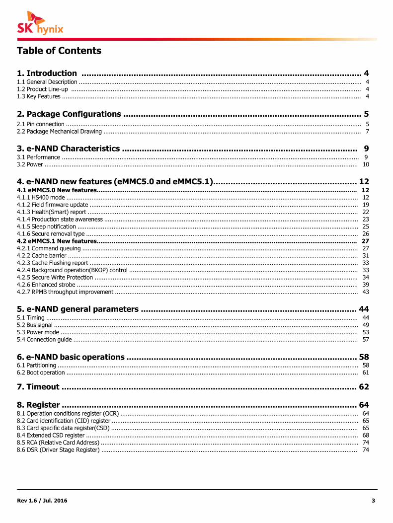
HS400 Device output timingData strobe is for reading data in HS400 mode. Data strobe is toggled only during data read or CRC status response.
[Figure 5] HS400 Device output timing
[Table 5] HS400 Device output timing
Parameter Symbol Min Max Unit Remark
Data Strobe
Cycle time datatransfer mode
tPERIOD 5200MHz(Max), between rising edges with respect to VT
Slew rate SR 1.125 V/ns With respect to VOH/VOL and HS400 reference load
Duty cycle distortion
tDSDCD 0.0 0.2 nsAllowable deviation from the input CLK duty cycle distortion(tCKDCD)With respect to VT Includes jitter, phase noise
Minimum pulse width
tDSMPW 2.0 ns With respect to VT
Read pre-amble tRPRE 0.4 5 (One Clock Cycle)
tPERIODMax value is specified by manufacturer.value up to infinite is valid.
Read post-amble tRPST 0.4 2.5 (Half Clock Cycle)
tPERIODMax value is specified by manufacturer.value up to infinite is valid.
Output DAT (referenced to Data strobe)
Output skew tRQ 0.4 ns With respect to VOH/VOL and HS400 reference load
Output hold skew tRQH 0.4 ns With respect to VOH/VOL and HS400 reference load
Slew rate SR 1.125 V/ns With respect to VOH/VOL and HS400 reference load

Rev 1.6 / Jul. 2016 15
[Table 6] HS400 Device input timing
Parameter Symbol Min Type Max Unit Remark
Pull-up resistance for CMD RCMD 4.7 100 Kohm
Pull-up resistance for DAT0-7 RDAT 10 100 Kohm
Pull-down resistance for Data strobe RDS 10 100 Kohm
Internal pull up resistance DAT1-DAT7 Rint 10 150 Kohm
Bus signal line capacitance CL 13 pF
Single Device capacitance CDevice 6 pF

Rev 1.6 / Jul. 2016 16
Data Strobe for HS400
Data strobe is Return Clock signal used in HS400 mode. This signal is generated by the device and used for data output and CRC status response output in HS400 mode. The frequency of this signal follows the frequency of CLK. For data output each cycle of this signal directs two bits transfer(2x) on the data - one bit for positive edge and the other bit for negative edge. For CRC status response output, the CRC status is latched on the positive edge only, and don't care on the negative edge. Data strobe signal is toggled only for Data out and CRC response (Align CMD response as well as CRC response to the DS in eMMC5.1)
[Figure 6] HS400 Host and Device block diagram
Rev 1.6 / Jul. 2016 17
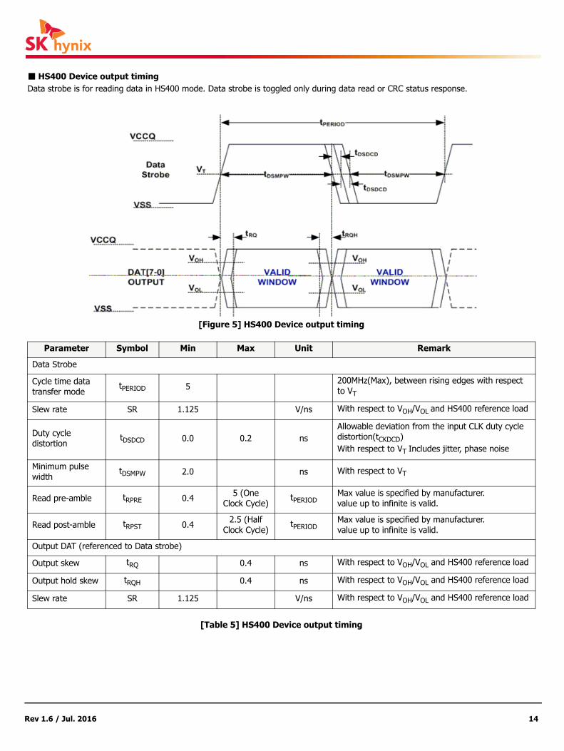
4.1.1.2 HS400 Mode selection
Following JEDEC standard for eMMC5.0, changing bus mode directly from HS200 to HS400 is not allowed. It has a rule for changing bus width from SDR mode to DDR mode that HS_TIMING must be set to “0x01”(HS mode : 52MHz) before setting BUS_WIDTH for DDR oper-ation. We recommend the HS400 bus mode selection sequence as following.(eMMC5.1 has basically same flow, but ‘enhanced strobe feature’ is added. Please refer to 4.2.6 Enhanced strobe)
[Figure 7] HS400 Bus mode selection sequence

Rev 1.6 / Jul. 2016 18
EXT_CSD register for Data strobe
• Enhanced Strobe field in BUS_WIDTH [183]
BIT[7] : 0: Strobe is provided only during data out and CTC response [Default] 1: Strobe is provided during data out, CRC response and CMD response
The support of STROBE_ENHANCED mode is optional for devices. STROBE_SUPPORT[184] register of EXT_CSD indicates whether a device supports that mode.
Bit 7 Bit 6 Bit 5 Bit 4 Bit 3 Bit 2 Bit 1 Bit 0
Enhanced Strobe Reserved Bus Mode Selection

Rev 1.6 / Jul. 2016 19
4.1.2 Field firmware update (FFU)
To download a new firmware, the e-NAND requires instruction sequence following JEDEC standard.SK hynix e-NAND only supports Manual mode (MODE_OPERATION_CODES is not supported). For more details, see as the following chart and register table given below.
[Figure 8] FFU flow chart
4.1.2.1 Field F/W update flow - CMD sequence
Operation CMD Remark
Set bus width (1bit or 4bit) Bus width should be 1bit or 4bit
Set block length 512B CMD16, arg : 0x00000200
Enter FFU mode CMD6, arg : 0x031E0100
Send FW to device(Download) CMD25, arg : 0xFFFAFFF0 Sending CMD25 is followed by sending FW data
CMD12 : Stop CMD12, arg : 0x00000000
CMD6 : Exit FFU mode CMD6, arg : 0x031E0000
CMD0/HW Reset/Power cycle
Re-Init to trans state CMD0, CMD1 ...
Check if FFU is succeeded CMD8, arg : 0x00000000Check EXT_CSD[26] : FFU_SUCCESS
If FFU_SUCCESS is 0, FFU is succeeded,otherwise FFU is failed.

Rev 1.6 / Jul. 2016 20
4.1.2.2 EXT_CSD Register for FFU
SUPPORTED_MODE[493] (Read Only)BIT[0] : ‘0’ FFU is not supported by the device. ‘1’ FFU is supported by the device.
BIT[1] : ‘0’ Vendor specific mode (VSM) is not supported by the device. ‘1’ Vendor specific mode is supported by the device.
FFU_FEATURE[492] (Read Only)BIT[0] : ‘0’ Device does not support MODE_OPERATION_CODES field (Manual mode)
‘1’ Device supports MODE_OPERATION_CODES field (Auto mode)
FF_ARG[490-487] (Read Only)Using this field the device reports to the host which value the host should set as an argument for read and write commands is FFU mode.
FF_CONFIG[169] (R/W)BIT[0] : Update disable
0x0 : FW updates enabled. / 0x01 : FW update disabled permanently
Bit Field Supportability
Bit[7:2] Reserved -
Bit[1] VSM Not support
Bit[0] FFU Supported
Bit Field Supportability
Bit[7:1] Reserved -
Bit[0] SUPPORTED_MODE_OPERATION_CODES Not supported
Bit Field Supportability
Bit[7:1] Reserved -
Bit[0] Update disable FW updates enabled (0x0)

Rev 1.6 / Jul. 2016 21
FFU_STATUS[26] (R/W/E_P)
Using this field the device reports to the host the state of FFU process.
OPERATION_CODES_TIMEOUT[491](Read Only)Maximum timeout for the SWITCH command when setting a value to the MODE_OPERATION_CODES field
The register is set to ‘0’, because the e-NAND doesn’t support MODE_OPERATION_CODES.
MODE_OPERATION_CODES[29] (W/E_P)The host sets the operation to be performed at the selected modes, in case MODE_CONFIGS is set to FFU_MODE,
MODE_OPERATION_CODES could have the following values :
Value Description
0x13 ~ 0xFF Reserved
0x12 Error in downloading Firmware
0x11 Firmware install error
0x10 General error
0x01 ~ 0x0F Reserved
0x00 Success
Value Description Timeout value
0x01 ~ 0x17 MODE_OPERATION_CODES_TIMEOUT = 100us x 2OPERATION_CODES_TIMEOUT 0 (Not defined)
0x18 ~ 0xFF Reserved -
Bit Description
0x01 FFU_INSTALL
0x02 FFU_ABOUT
0x00, others Reserved

Rev 1.6 / Jul. 2016 22
4.1.3 Health(Smart) report
Using this feature is for monitoring device status and preventing the error and failure in advance.Host can check device information with EXT_CSD as the register table given below.
[Table 7] Using EXT_CSD for health report (Read only)
Field CSD slice Description
VENDOR_PROPRIETARY_HEALTH_REPORT [301:270] Reserved for vendor proprietary health report. (NONE)
DEVICE_LIFE_TIME_EST_TYPE_ A/B [268:269] Current average P/E cycle of memory of Type A(SLC) / Type B(MLC)relative to its maximum estimated capability
PRE_EOL_INFO [267] Consumed reserved blocks to notify before reaching the EOL (End of life) status
OPTIMAL_TRIM/WRITE_READ_SIZE [264:266] Minimum optimal (for the device) Erase / Write / Read unit size for the different partitions
DEVICE_VERSION [263:262] Device version
FIRMWARE_VERSION [261:254] Device FW version
Rev 1.6 / Jul. 2016 23
4.1.4 Production state awareness
This new feature is added for eMMC5.0 JEDEC Spec. to prevent the data break during device soldering. For this feature implementation, e-NAND supports only manual mode and PRODUCT_STATE_AWARENESS_TIMEOUT is 0x17(maximum). For more detail, see as the flow chart and register table given below.
[Figure 9] Production State Awareness manual mode flowchart
PRODUCTION_STATE_AWARENESS_TIMEOUT[218] (Read Only)This field indicates maximum timeout for the SWITCH command when setting a value to thePRODUCTION_STATE_AWARENESS[133]field
Value Description Timeout value
0x01 ~ 0x17 Production State Timeout = 100us x 2PRODUCTION_STATE_AWARENESS_TIMEOUT 0x17 (838.86s)
0x18 ~ 0xFF Reserved -

Rev 1.6 / Jul. 2016 24
PRODUCTION_STATE_AWARENESS[133](R/W/E)
e-NAND doesn’t support 0x03 state.
PRODUCTION_STATE_ENABLEMENT[17]
e-NAND only supports manual mode for PRODUCTION_STATE_AWARENESS
Value Device State Description
0x00 NORMAL (Field) Regular operation
0x01 PRE_SOLDERING_WRITES -
0x02 PRE_SOLDERING_POST_WRITES Once transferred to this state the host should not write content to the device
0x03 AUTO_PRE_SOLDERING Not supported
0x04 ~ 0x0F Reserved -
0x10 ~ 0x1F Reserved for Vendor Proprietary Usage -
Enablement(R/W/E) Capabilities(R)
Bit7 Bit6 Bit5 Bit4 Bit3 Bit2 Bit1 Bit0
Reserved Mode
Production State
Awareness enable
Reserved Auto modeSupported
Manual mode Supported
Cleared when PRODUCTION_STATE_AWARENESS is charged to Normal (either automatically or by setting
PRODUCTION_STATE_AWARENESS to Normal)
This bit could be set to ‘1’ only once

Rev 1.6 / Jul. 2016 25
4.1.5 Sleep notification
Host may use to a power off notification when it intends to turn-off Vcc After moving the device to sleep state. Some features are added to clarify the spec for entering sleep mode when power off notification is enabled.
Add the SLEEP_NOTIFICATION on the interruptible Command List
SLEEP_NOTIFICATION_TIME[216](Read Only)Maximum timeout for the SWITCH command when notifying the device that it is about to move to sleep state by writing SLEEP_NOTIFICATION to POWER_OFF_NOTIFICATION[34]byte. (unit : 10us)
POWER_OFF_NOTIFICATION[34]
Add Ox04h for the SLEEP_NOTIFICATION as a valid value
CMD Description Is interruptible?
CMD6 SWITCH, Byte POWER_OFF_NOTIFICATION, Value POWER_OFF_LONG or SLEEP_NOTIFICATION Yes
Value Description Timeout value
0x01 ~ 0x17 Sleep Notification Timeout = 10us x 2 SLEEP_NOTIFICATION_TIME 0xC (40.96ms)
0x18 ~ 0xFF Reserved -
Value Field Description
: : :
0x03 POWER_OFF_LONG Host is going to power off the device.The device shall respond within POWER_OFF_LONG_TIME
0x04 SLEEP_NOTIFICATION Host is going to put device in sleep mode. The device shall respond within SLEEP_NOTIFICATION_TIME

Rev 1.6 / Jul. 2016 26
4.1.6 Secure removal type
This feature is used for how information is removed from the physical memory during a purge operation.
Secure Removal Type[16]Among four options for secure removal type, e-NAND supports 0x3, 0x1 and 0x0 (0x2 option is not supported)e-NAND recommends using a vendor defined removal type(type 3). If host want to erase the device physically using removal type0.Secure erase & Secure trim time is longer than using removal type0
BIT Description of Secure Removal Type Description Supportability
BIT[5:4] Configure Secure Removal Type (R/W)
0x3 Information removed using a vendor defined Support
0x2Information removed by an overwriting the addressed locations with a character, its complement, then a random character
-
0x1Information removed by an overwriting the addressed locations with a character followed by an erase
-
0x0 Information removed by an erase of the physical memory -
BIT[3:0] Supported Secure Removal Type (R)
BIT[3] Information removed using a vendor defined Support
BIT[2]Information removed by an overwriting the addressed locations with a character, its complement, then a random character
Not support
BIT[1]Information removed by an overwriting the addressed locations with a character followed by an erase
Support
BIT[0] Information removed by an erase of the physical memory Support

Rev 1.6 / Jul. 2016 27
4.2 eMMC5.1 New features
4.2.1 Command queuing
e-NAND manages an internal task queue to which the host can queue data transfer tasks to efficient operate.
4.2.1.1 CMD list for Command queuing
Index Abbreviation Argument Remark
CMD44 Queued Task parameter
[31] Reliable Write Request[30] Data Direction (Read=1, Write=0)[29] Tag Request[28:25] context ID[24]Forced Programming[23] Priority ( simple =0, high=1)[20:16] Task ID(31~0)[15:0] # of BLK
Encodes parameter which are necessary for queuing the task and executing the transfer
CMD45 Queued Task Address [31:0] Block address for the transaction The host instructs the device to queue a data transfer task
CMD46 Execute Read Task [20:16] Task ID of therequested task which is must marked as “ready for execution” in the Queue Status Register
In order to execute a data read task (CMD46) or write task(CMD47) which is already queuedCMD47 Execute Write Task
CMD48 CMDQ_TASK_MGMT
[31:21] reserved [20:16]: TaskID [15:4]: reserved [3:0] TM op-code
Device shall discard a specific task or entire queue (all tasks in the queue) [20:16] when TM op-code = 2h these bits represent TaskID. When TM op-code=1h these bits are reserved.
Index Abbreviation Argument Remark
CMD13 SEND_STATUS
[31:16] RCA [15] SQS[14] Stuff bits[0] HPI
In case SQS bit = 1: indicate that this is CMD13 of CMD Queue. In response device shall send the QSR. In this case HPI bit muse be set to ‘0’.

Rev 1.6 / Jul. 2016 28
4.2.1.2 EXT_CSD Register for Command queuing
CMDQ_SUPPORT[308](Read only)This field indicates whether command queuing is supported by the device.
BIT[0]: 0: Command queuing is not supported
1: Command queuing is supported
CMDQ_DEPTH[307](Read only)This field is used to calculate the depth of the queue supported by the device. The maximum depth allowed by the standard is 32. The range of allowed Task IDs is 0 through N.
BIT[4:0]: N, a parameter used to calculate the Queue Depth of task queue in the device.
Queue Depth = N+1.
CMDQ_MODE_EN[15](R/W)This field is used by the host enable command queuing mechanism if supported by the device.
BIT[0]: 0: Command queuing is disabled. Host should clear the queue empty using CMD48 prior disabling the queue.
1: Command queuing is enabled
To maintain backward compatibility with hosts, which do not support command queuing, when the command queuing is disabled other functionality of the device is as if the device does not support command queuing.
Bit Field Supportability
Bit[7:1] Reserved -
Bit[0] CMDQ Support Supported (0x1)
Bit Field CMD queue depth value
Bit[7:5] Reserved -
Bit[4:0] N N=31 (0x1F)
Bit Field Supportability
Bit[7:1] Reserved -
Bit[0] CMDQ enable -

Rev 1.6 / Jul. 2016 29
4.2.1.3 New register for Command queuing
QSR (Queue Status Register)
The 32bit QSR carries the state of tasks in the queue at a specific point in time.
The host has read access to this register through device response to SEND_STATUS command(CMD13 with bit[15]=”1”), R1’s argument
will be the QSR.
Every bit in the QSR represents the task who’s ID corresponds to the bit index.
If bit QSR[i]=‘0’, the queued task with a Task ID i is not ready for execution.
The task may be queued and pending, or the Task ID is unused.
If bit QSR[i]=‘1’, the queued task with Task ID i is ready for execution.

Rev 1.6 / Jul. 2016 30
4.2.1.4 Command queuing Flows

Rev 1.6 / Jul. 2016 31
4.2.2 Cache Barrier
There are cases where the host is not interested in flushing the data right away, however it would like to keep an order between different cached data.The flushing can be delayed by the device to some later idle time. Barrier commands avoid the long delay by flush commands.
4.2.2.1 EXT_CSD Register for Cache Barrier
BARRIER_SUPPORT[488](Read only)This field indicates whether the device supports the barrier command.
BIT[7:0]: 0: Barrier command is not supported
1: Barrier command is supported
FLUSH_CACHE[32](W/E_P)A barrier command is issued by setting BARRIER bit. All data cached before the barrier shall be flushed to the non-volatile memory before any request after the barrier command. Data in the cache shall be flushed to the non-volatile storage by setting the FLUSH bit.
BIT[1]: 0: Reset value 1: Set barrier
BIT[0]: 0: Reset value
1: Triggers the flush
Bit Field Supportability
Bit[7:0] BARRIER_SUPPORT Supported (0x1)
Bit Field Supportability
Bit[7:2] Reserved -
Bit[1] BARRIER -
Bit[0] FLUSH -
Flush
Rev 1.6 / Jul. 2016 32
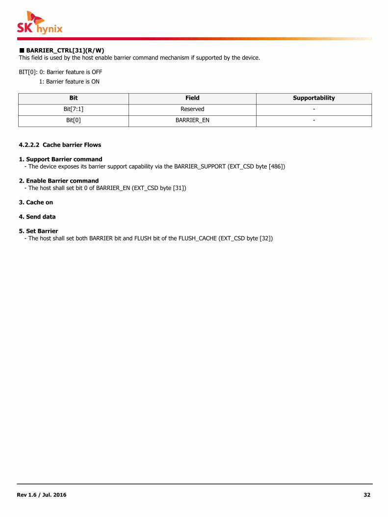
BARRIER_CTRL[31](R/W)This field is used by the host enable barrier command mechanism if supported by the device.
BIT[0]: 0: Barrier feature is OFF
1: Barrier feature is ON
4.2.2.2 Cache barrier Flows
1. Support Barrier command - The device exposes its barrier support capability via the BARRIER_SUPPORT (EXT_CSD byte [486])
2. Enable Barrier command - The host shall set bit 0 of BARRIER_EN (EXT_CSD byte [31])
3. Cache on
4. Send data
5. Set Barrier - The host shall set both BARRIER bit and FLUSH bit of the FLUSH_CACHE (EXT_CSD byte [32])
Bit Field Supportability
Bit[7:1] Reserved -
Bit[0] BARRIER_EN -

Rev 1.6 / Jul. 2016 33
4.2.3 Cache Flushing Report
For devices which flush cached data in an in-order manner, cache barrier commands are redundant and impose a needless overhead to the device and host.
4.2.3.1 EXT_CSD Register for Cache Flushing Report
CACHE_FLUSH_POLICY[240](Read only)BIT[0]: 0: Device flushing policy is not provided by the device.
1: Device is using a FIFO policy for cache flushing
4.2.4 BKOP Control
This feature allows the host to indicate to the device if it is expected to periodically manually start background operations by writing to the BKOPS_START field.
4.2.4.1 EXT_CSD Register for BKOP Control
BKOP_EN[163](R/W/E, R/W)
BIT[1](R/W/E): 0: Device shall not perform background operations while not servicing the host. 1: Device may perform background operations while not servicing the host.
BIT[0] (R/W): 0: Host does not support background operations handling and is not expected to write to BKOPS_START field.
1: Host is indicating that it shall periodically write to BKOPS_START field to manually start background operations.
Bit Field Supportability
Bit[7:1] Reserved -
Bit[0] FIFO Supported (0x01)
Bit Field Supportability
Bit[7:2] Reserved -
Bit[1] AUTO_EN -
Bit[0] MANUAL_EN -

Rev 1.6 / Jul. 2016 34
4.2.5 Secure Write Protection
Any application running on the host may issue write protection by updating fields of write protection related EXT_CSD, like USER_WP[171], BOOT_WP[173], by issuing CMD6, CMD8, CMD28 and CMD29 (Legacy mode). However there are weak points in the legacy mode. To prevent un-authorized changes, host should enter the secure write protect mode
• In Secure WP Mode, WP related EXT_CSDs (EXT_CSD[171],[173]) can be updated only if SECURE_WP_MASK fields is 0x1.
• Secureness is provided by allowing only RPMB method to update the register for SECURE_WP_MASK.
• Automatic Write protection mode is added to prevent security hole by power-control security attack.
SECURE_WP_INFO[211]
Updated by CMD6 when SECURE_WP_MASK is 0x1.
All legacy WP related commands works when SECURE_WP_MASK is 0x1.

Rev 1.6 / Jul. 2016 35
4.2.5.1 EXT_CSD Register for Secure Write Protection
SECURE_WP_INFO[211](Read Only)The SECURE_WP_SUPPORT field indicates whether the device is supporting secure write protection mode. The SECURE_WP_EN_STATUS is showing the value of SECURE_WP_EN defined in Authenticated Device Configuration Area.
BIT[1] 0: Legacy Write Protection mode 1: Secure Write Protection mode
BIT[0] 0: Secure Write Protection is NOT supported by this device
1: Secure Write Protection is supported by this device
4.2.5.2 New register for Secure Write Protection
Authenticated Device Configuration Area
• Hidden register instead of EXT_CSD register for SECURE_WP_MODE_CONFIG, ENABLE.
• Those two SECURE_WP_MODE_CONFIG and SECURE_WP_MODE_ENABLE registers are defined in Device Configuration area, and
those register should be updated only by Authenticated Device Configuration write request. (RPMB)
Bit Field Supportability
Bit[7:2] Reserved -
Bit[1] SECURE_WP_EN_STATUS -
Bit[0] SECURE_WP_SUPPROT Supported (0x01)
Name Field Size (Bytes) Cell Type Address
Reserved 253 - [255:3]
Secure Write Protect Configuration SECURE_WP_MODE_CONFIG 1 R/W/E_P [2]
Secure Write Protect Enable SECURE_WP_MODE_ENABLE 1 R/W/E [1]
Reserved 1 [0]

Rev 1.6 / Jul. 2016 36
Authenticated Device Configuration Area (1) : SECURE_WP_MODE_ENABLE (R/W/E)
The byte is to enter/exit the secure write protection mode. If host want a device to enter the secure Write Protection mode, host set the SECURE_WP_EN bit as ‘0x1’ in this register using Authen-ticated Device Configuration Write request. This register can be read using Authenticated Device Configuration Read request. If there are already write protected groups or write protected boot partitions, those will be preserved when entering or exiting secure Write pro-tected mode.
Bit [0] 0: Legacy Write Protection mode. (TMP_WRITE_PROTECT[12] , PERM_WRITE_PROTECT[13] is updated by CMD27. USER_WP[171], BOOT_WP[173] and BOOT_WP_STATUS[174] are updated by CMD6.)
1: Secure Write Protection mode. (The access to the write protection related EXT_CSD and CSD fields depends on the value of SECURE_WP_MASK bit in SECURE_WP_MODE_CONFIG field.)
The default value of this field is 0x0.
Bit Field Supportability
Bit[7:1] Reserved -
Bit[0] SECURE_WP_MODE_ENABLE -

Rev 1.6 / Jul. 2016 37
Authenticated Device Configuration Area (2) : SECURE _WP_MODE_CONFIG (R/W/E_P)
In secure write protected mode, the updatability of USER_WP[171], BOOT_WP[173], TMP_WRITE_PROTECT[12] and PERM_WRITE_PROTECT[13] are controlled by this mask value. Bit [0] 0: Disabling updating WP related EXT_CSD and CSD fields. CMD27 (Program CSD) will generate generic error for setting TMP_WRITE_PROTECT[12] , PERM_WRITE_PROTECT[13]. CMD6 for updating USER_WP[171], BOOT_WP[173] and BOOT_WP_STATUS[174] generates SWITCH_ERROR. If a force erase command is issued, the command will fail (Device stays locked) and the LOCK_UNLOCK_FAILED error bit will be set in the status register. If CMD28 or CMD29 is issued, then generic error will be occurred. Power-on Write Protected boot partitions will keep protected mode after power failure, H/W reset assertion and any CMD0 reset. The device keeps the current value of BOOT_WP in the EXT_CSD register to be same after power cycle, H/W reset assertion, and any CMD0 reset.
1: Enabling updating WP related EXT_CSD and CSD fields. (TMP_WRITE_PROTECT[12] , PERM_WRITE_PROTECT[13] , USER_WP[171], BOOT_WP[173] and BOOT_WP_STATUS[174] are accessed using CMD6, CMD8 and CMD27. If a force erase command is issued and accepted, then ALL THE DEVICE CONTENT WILL BE ERASED including the PWD and PWD_LEN register content and the locked Device will get unlocked. If a force erase command is issued and power-on protected or a permanently-write-protected write protect groups exist on the device, the command will fail (Device stays locked) and the LOCK_UNLOCK_FAILED error bit will be set in the status register. An attempt to force erase on an unlocked Device will fail and LOCK_UNLOCK_FAILED error bit will be set in the status register. Write Protection is applied to the WPG indicated by CMD28 with the WP type indicated by the bit[2] and bit[0] of USER_WP[171]. All temporary WP Groups and power-on Write Protected boot partitions become writable/erasable temporarily which means write protect type is not changed. All power-on and permanent WP Groups in user area will not become writable/ erasable temporarily. Those temporarily writable/erasable area will become write protected when this bit is cleared to 0x0 by the host or when there is power failure, H/W reset assertion and any CMD0 reset. The device keeps the current value of BOOT_WP CSD register to be same after power cycle, H/W reset assertion, and any CMD0 reset.)
The default value of this field is 0x0.
Bit Field Supportability
Bit[7:1] Reserved -
Bit[0] SECURE_WP_MODE_CONFIG -
Rev 1.6 / Jul. 2016 38
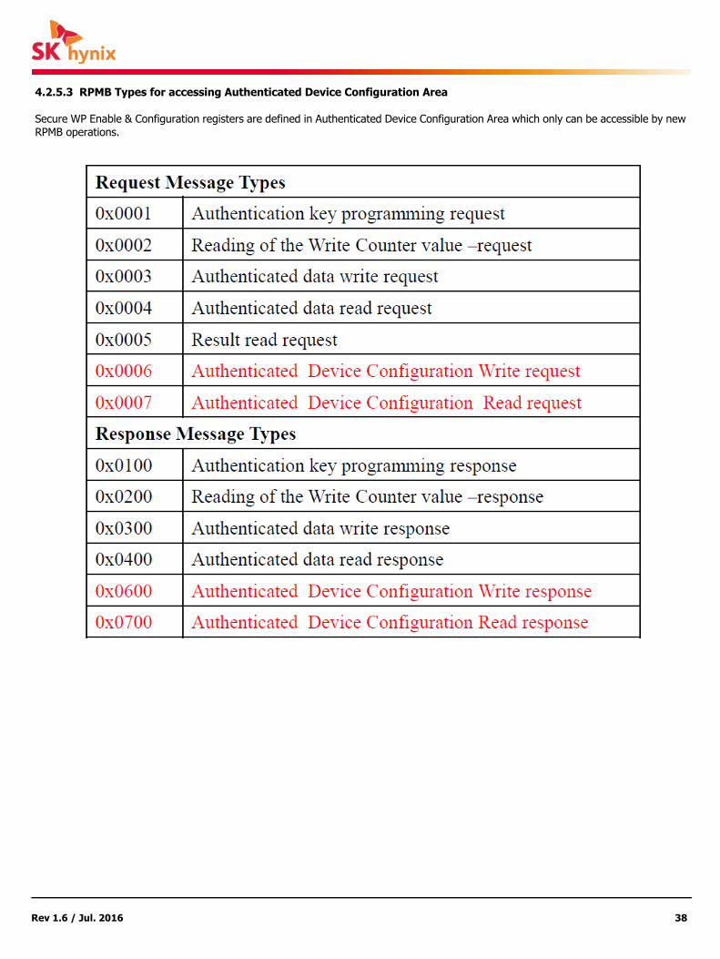
4.2.5.3 RPMB Types for accessing Authenticated Device Configuration Area
Secure WP Enable & Configuration registers are defined in Authenticated Device Configuration Area which only can be accessible by new RPMB operations.

Rev 1.6 / Jul. 2016 39
4.2.6 Enhanced strobe
In Enhanced Strobe mode DATA OUT, CRC Response and CMD Response are all synched to STROBE clocks. The timing relation between CMD Response output signals and STROBE clocks is the same as defined for DATA Out to STROBE clocks.
[Figure 10] HS400 Host and Device block diagram (when Enhanced Strobe is enabled)

Rev 1.6 / Jul. 2016 40
[Figure 11] Enhanced Strobe signals for CMD Response and Data Out (Read operation)
[Figure 12] Enhanced Strobe signals for CMD Response and Data Out (Write operation)
[Figure 13] HS400 mode change with Enhanced Strobe

Rev 1.6 / Jul. 2016 41
4.2.6.1 EXT_CSD Register for Enhanced Strobe
STROBE_SUPPORT[184](Read only)This register indicates whether a device supports Enhanced Strobe mode for operation modes that STROBE is used for HS400.
BIT[7:0]: 0: Indicates No support of Enhanced Strobe mode
1: Indicates the device supports Enhanced Strobe mode
Bit Field Supportability
Bit[7:0] STROBE_SUPPORT Supported (0x01)

Rev 1.6 / Jul. 2016 42
4.2.6.2 HS400 mode (Enhanced Strobe) selection
This selection flow describes how to initialize the eMMC device in HS400 mode while enabling Enhanced Strobe without the need for tun-ing procedure. After the host initializes the device, host check whether the device supports the HS400 mode and Enhanced Strobe by reading the DEVICE_TYPE and STROBE_SUPPORT fields in the Extended CSD register. After power-on or software reset (CMD0), the interface timing of the device is set as the default ‘Backward Compatible Timing’. In order to switch to HS400 mode with Enhanced Strobe, host should perform the following steps.
[Figure 14] HS400 Bus mode (Enhanced Strobe) selection flow diagram

Rev 1.6 / Jul. 2016 43
4.2.7 RPMB throughput improvement
This feature is proposed for RPMB write data size to improve the RPMB throughput in eMMC5.1 spec. In the eMMC5.0 spec, REL_WR_SEC_C[222] register shall be set to 1 (hence the granularity is always 512B.)- For reliable write to RPMB partition, there is limitation that block count can not exceed the size of REL_WR_SEC_C x 512B. In eMMC5.1, the supported RPMB write access size is 256B, 512B, and 8KB.
WRITE_REL_PARAM (EXT_CSD[166]): Read only
When EXT_CSD[166][4] (R) = 0
- Device does not support large RPMB wirte transfer- The behavior is same as eMMC v5.0 or earlier
When EXT_CSD[166][4] (R) = 1
- Device supports large RPMB wirte transfer- Host transfers small RPMB write with block count = 1 or 2 (256/512B)- Host transfers large RPMB write with block count = 32 (8KB) * the start address should be 8KB aligned, and the transferred data (8KB) is all-new or all-old
Bit Field Supportability
Bit[4] EN_RPMB_REL_WR Supported (0x01)

Rev 1.6 / Jul. 2016 44
5. e-NAND general parameters
5.1 Timing
5.1.1 Bus timing
Data must always be sampled on the rising edge of the clock.
[Figure 15] Timing diagram: data input/output

Rev 1.6 / Jul. 2016 45
[Table 9] High-speed e-NAND interface timing
• CLK timing is measured at 50% of VDD.
• e-NAND shall support the full frequency range from 0-26Mhz, or 0-52MHz
• CLK rising and falling times are measured by min (VIH) and max (VIL).
• Input CMD, DAT rising and falling times are measured by min (VIH) and max (VIL), and output CMD, DAT rising and falling times
are measured by min (VOH) and max (VOL).
Parameter Symbol Min Max Unit Remark
Clock CLK
Clock frequency data transfer mode (PP) fPP 0 52 MHz CL ≤30 pFTolerance: +100KHz
Clock frequency identification mode (OD) fOD 0 400 KHz Tolerance: +20KHz
Clock high time tWH 6.5 ns CL ≤ 30 pF
Clock low time tWL 6.5 ns CL ≤ 30 pF
Clock rise time tTLH 3 ns CL ≤ 30 pF
Clock fall time tTHL 3 ns CL ≤ 30 pF
Inputs CMD, DAT (referenced to CLK)
Input set-up time tISU 3 ns CL ≤ 30 pF
Input hold time tIH 3 ns CL ≤ 30 pF
Outputs CMD, DAT (referenced to CLK)
Output delay time during data transfer tODLY 13.7 ns CL ≤ 30 pF
Output hold time tOH 2.5 ns CL ≤ 30 pF
Signal rise time tRISE 3 ns CL ≤ 30 pF
Signal fall time tFALL 3 ns CL ≤ 30 pF

Rev 1.6 / Jul. 2016 46
[Table 10] Backward-compatible e-NAND interface timing
• e-NAND must always start with the backward-compatible interface timing. The timing mode can be switched to
high-speed timing by the host sending the switch command (CMD6) with the argument for high speed interface select.
• CLK timing is measured at 50% of VDD.
• CLK rising and falling times are measured by min (VIH) and max (VIL).
• tOSU and tOH are defined as values from clock rising edge. However, there may be cards or devices which utilize clock falling edge to
output data in backward compatibility mode.
Therefore, it is recommended for hosts either to set tWL value as long as possible within the range which should not go over
tCK-tOH(min) in the system or to use slow clock frequency, so that host could have data set up margin for those devices.
In this case, each device which utilizes clock falling edge might show the correlation either between tWL and tOSU or between
tCK and tOSU for the device.
Parameter Symbol Min Max Unit Remark
Clock CLK
Clock frequency data transfer mode (PP) fPP 0 26 400 CL ≤30 pF
Clock frequency identification mode (OD) fOD 0 400 KHz
Clock high time tWH 10 ns CL ≤ 30 pF
Clock low time tWL 10 ns CL ≤ 30 pF
Clock rise time tTLH 10 ns CL ≤ 30 pF
Clock fall time tTHL 10 ns CL ≤ 30 pF
Inputs CMD, DAT (referenced to CLK)
Input set-up time tISU 3 ns CL ≤ 30 pF
Input hold time tIH 3 ns CL ≤ 30 pF
Outputs CMD, DAT (referenced to CLK)
Output set-up time tOSU 11.7 ns CL ≤ 30 pF
Output hold time tOH 8.3 ns CL ≤ 30 pF
Rev 1.6 / Jul. 2016 47
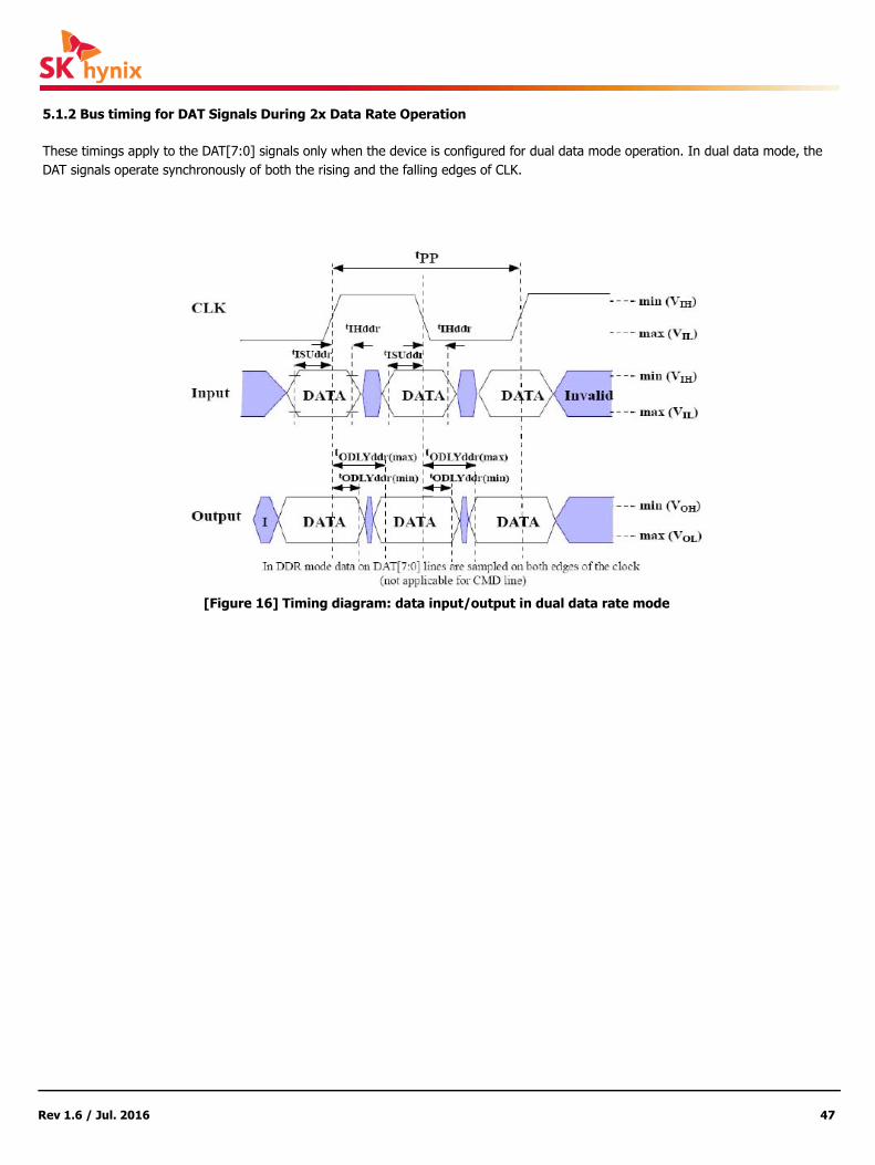
5.1.2 Bus timing for DAT Signals During 2x Data Rate Operation
These timings apply to the DAT[7:0] signals only when the device is configured for dual data mode operation. In dual data mode, the DAT signals operate synchronously of both the rising and the falling edges of CLK.
[Figure 16] Timing diagram: data input/output in dual data rate mode

Rev 1.6 / Jul. 2016 48
[Table 11] Dual data rate interface timings
• NOTE 1. CLK timing is measured at 50% of VDD.• NOTE 2. Inputs DAT rising and falling times are measured by min (VIH) and max (VIL), and outputs CMD, DAT rising and falling
times are measured by min (VOH) and max (VOL)
Parameter Symbol Min. Max. Unit Remark
Input CLK(1)
Clock duty cycle 45 55 % Includes jitter, phase noise
Clock rise time tTLH 3 ns CL≤30 pF
Clock fail time tTHL 3 ns CL≤30 pF
Input CMD (referenced to CLK-SDR mode)
Input set-up time tISUddr 3 ns CL≤20 pF
Input hold time tIHDDR 3 ns CL≤20 pF
Output CMD (referenced to CLK-SDR mode)
Output delay time during data transfer tODLY 13.7 ns CL≤20 pF
Output hold time tOH 2.5 ns CL≤20 pF
Signal rise time tRISE 3 ns CL≤20 pF
Signal fall time tFALL 3 ns CL≤20 pF
Input DAT (referenced to CLK-DDR mode)
Input set-up time tISUddr 2.5 ns CL≤20 pF
Input hold time tIHddr 2.5 ns CL≤20 pF
Outputs DAT (referenced to CLK-DDR mode)
Output delay time during data transfer tODLYddr 1.5 7 ns CL≤20 pF
Signal rise time(DAT0-7)(2) tRISE 2 ns CL≤20 pF
Signal fall time (DAT0-7) tFALL 2 ns CL≤20 pF

Rev 1.6 / Jul. 2016 49
5.2 Bus signal
5.2.1 Bus signal line load
The total capacitance CL of each line of e-MMC bus is the sum of the bus master capacitance CHOST, the bus capacitance CBUS itself, and
the capacitance CDevice of the eMMC connected to this line, and requiring the sum of the host and bus capacitances not to exceed 20 pF.
CL = CHOST + CBUS + CDevice
[Table 12] e-NAND capacitance
Parameter Symbol Min Typ Max Unit Remark
Pull-up resistance for CMD RCMD 4.7 100 Kohm to prevent bus floating
Pull-up resistance for DAT0-7 RDAT 10 100 Kohm to prevent bus floating
Internal pull up resistanceDAT1 - DAT7
Rint 10 150 Kohm
Bus signal line capacitance CL 30 pF Single Device
Single Device capacitance CDEVICE 6 pF
Maximum signal lineinductance
16 nH fPP ≤ 52 MHz
VDDi capacitor value CREG
0.1 uF
To stabilize regulator output when target device bus speed mode is either backward-compatible, high speed SDR, high speed DDR, or HS200.
1 uFTo stabilize regulator output when target device bus speed mode is HS400
Vccq decoupling capacitor CH1 1 uF

Rev 1.6 / Jul. 2016 50
5.2.2 Overshoot / Undershoot specification
[Table 13] Overshoot / Undershoot specification
[Figure 17] Overshoot / Undershoot definition
SpecificationVccq
Unit1.70V - 1.95V
Maximum peak amplitude allowed for overshoot area. Max 0.9 V
Maximum peak amplitude allowed for undershoot area. Max 0.9 V
Maximum area above Vccq Max 1.5 V-ns
Maximum area below Vssq Max 1.5 V-ns

Rev 1.6 / Jul. 2016 51
5.2.3 Bus Signal levels
As the bus can be supplied with a variable supply voltage, all signal levels are related to the supply voltage.
[Figure 18] e-NAND bus signal level
• Open-Drain mode bus signal level
[Table 14] Open-Drain signal level
• NOTE 1. Because Voh depends on external resistance value (including outside the package), this value does not apply as device
specification. Host is responsible to choose the external pull-up and open drain resistance value to meet Voh minimum value.
Parameter Symbol Min. Max. Unit Conditions
Output high voltage VOH VDD - 0.2 V Note1)
Output low voltage VOL 0.3 V IOL = 2mA

Rev 1.6 / Jul. 2016 52
• Push-Pull mode bus signal level
The device input and output voltages shall be within the following specified ranges for any VDD of the allowed voltage range
[Table 15] Push-Pull signal level 2.7V-3.6V Vccq range
[Table 16] Push-pull signal level 1.65V-1.95V Vccq range
Parameter Symbol Min. Max. Unit Conditions
Output HIGH voltage VOH 0.75 * Vccq V IOH = -100µA @ Vccq min
Output LOW voltage VOL 0.125 * Vccq V IOL = -100µA @ Vccq min
Input HIGH voltage VIH 0.625 * Vccq Vccq + 0.3 V
Input LOW voltage VIL VSS - 0.3 0.25 * Vccq V
Parameter Symbol Min. Max. Unit Conditions
Output HIGH voltage VOH Vccq - 0.45V V IOH = -2mA
Output LOW voltage VOL 0.45V V IOL = -2mA
Input HIGH voltage VIH 0.65 * Vccq Vccq + 0.3 V
Input LOW voltage VIL VSS - 0.3 0.35 * Vccq V

Rev 1.6 / Jul. 2016 53
5.3 Power mode
5.3.1 e-NAND power-up guidelines
e-NAND power-up must adhere to the following guidelines:
• When power-up is initiated, either Vcc or Vccq can be ramped up first, or both can be ramped up simultaneously.
• After power up, e-NAND enters the pre-idle state. The power up time of each supply voltage should be less than the specified tPRU (tPRUH, tPRUL or tPRUV) for the appropriate voltage range.
• If e-NAND does not support boot mode or its BOOT_PARTITION_ENABLE bit is cleared, e-NAND moves immediately to the idle state. While in the idle state, e-NAND ignores all bus transactions until receiving CMD1. e-NAND begins boot operation with the argument of 0xFFFFFFFA. If boot acknowledge is finished, e-NAND shall send acknowledge pattern “010” to the host within the specified time. After boot operation is terminated, e-NAND enters the idle state and shall be ready for CMD1 operation. If e-NAND receives CMD1 in the pre-boot state, it begins to respond to the command and moves to the card identification mode.
• When e-NAND is initiated by alternative boot command(CMD0 with arg=0xFFFFFFFA), all the data will be read from the boot partition and then e-NAND automatically goes to idle state, but hosts are still required to issue CMD0 with arg=0x0000000000 in order to complete a boot mode properly and move to the idle state. While in the idle state, e-NAND ignores all bus transactions until it receives CMD1.
• CMD1 is a special synchronization command which is used to negotiate the operating voltage range and poll the device until it is out of its power-up sequence. In addition to the operating voltage profile of the device, the response to CMD1 contains a busy flag indicating that the device is still working on its power-up procedure and is not ready for identification. This bit informs the host that the device is not ready, and the host must wait until this bit is cleared. The device must complete its initialization within 1 second of the first CMD1 issued with a valid OCR range.
• If the e-NAND device was successfully partitioned during the previous power up session (bit 0 of EXT_CSD byte [155]PARTITION_SETTING_COMPLETE successfully set) then the initialization delay is (instead of 1s) calculated from INI_TIMEOUT_PA (EXT_CSD byte [241]). This timeout applies only for the very first initialization after successful partitioning. For all the consecutive initialization 1sec time out will be applied.
• The bus master moves the device out of the idle state. Because the power-up time and the supply ramp-up time depend on the application parameters such as the bus length and the power supply unit, the host must ensure that power is built up to the operating level (the same level that will be specified in CMD1) before CMD1 is transmitted.
• After power-up, the host starts the clock and sends the initializing sequence on the CMD line. The sequence length is the longest of: 1ms, 74 clocks, the supply ramp-up time, or the boot operation period. An additional 10 clocks (beyond the 64 clocks of the power-up sequence) are provided to eliminate power-up synchronization problems.
• Every bus master must implement CMD1.

Rev 1.6 / Jul. 2016 54
5.3.2 e-NAND Power Cycling
The master can execute any sequence of Vcc and Vccq power-up/power-down. However, the master must not issue any commands until
Vcc and Vccq are stable within each operating voltage range. After the slave enters sleep mode, the master can power-down Vcc to
reduce power consumption. It is necessary for the slave to be ramped up to Vcc before the host issues CMD5 (SLEEP_AWAKE) to wake
the slave unit.
[Figure 19] e-NAND power cycle
If Vcc or Vccq is below 0.5 V for longer than 1 ms, the slave shall always return to the pre-idle state, and perform the appropriate boot
behavior. The slave will behave as in a standard power up condition once the voltages have returned to their functional ranges. An exception to this behavior is if the device is in sleep state, in which the voltage on Vcc is not monitored.

Rev 1.6 / Jul. 2016 55
5.3.3 Leakage
[Table 17] General operation conditions
5.3.4 Power Supply
In e-NAND, Vcc is used for the NAND core voltage and NAND interface; Vccq is for the controller core and e-NAND interface voltage
shown in Figure 15. The core regulator is optional and only required when internal core logic voltage is regulated from Vccq. A Creg
capacitor must be connected to the VDDi terminal to stabilize regulator output on the system.
[Figure 20] e-NAND internal power diagram
Parameter Symbol Min Max. Unit Remark
BGA -0.5 Vccq+0.5 V
All inputs
Input leakage current (before initialization sequenceand/or the internalpull up resistors connected)
-100 100
All outputs
Output leakage current (before initialization sequence) -100 100
Output leakage current (after initialization sequence) -2 2
A
A
A

Rev 1.6 / Jul. 2016 56
e-NAND supports one or more combinations of Vcc and Vccq as shown in Table 18.
The available voltage configuration is shown in Table 19.
[Table 18] e-NAND power supply voltage
[Table 19] e-NAND voltage combinations
• NOTE 1. VccQ(I/O) 3.3 volt range is not supported in either HS200 or HS400 devices.
Parameter Symbol Min Max. Unit Remark
Supply voltage (NAND) Vcc2.7 3.6 V
1.7 1.95 V Not supported
Supply voltage (I/O) Vccq2.7 3.6 V
1.7 1.95 V
Supply power-up for 3.3V tPRUH 35 ms
Supply power-up for 1.8V tPRUL 25 ms
Vccq
1.7V ~ 1.95V 2.7V ~ 3.6V
Vcc2.7V–3.6V Valid Valid (1)
1.7V–1.95V Not Valid Not Valid

Rev 1.6 / Jul. 2016 57
5.4 Connection Guide
[Figure 21] Connection guide drawing
[Table 20] Connection guide specification
Parameter Symbol Min Max Recommend Unit Remark
Pull-up resistance for CMD R_CMD 4.7 100 10 kohm Pull-up resistance should be put on CMD line to
prevent bus floating.
Pull-up resistance for DAT0~7 R_DAT 10 100 50 kohm Pull-up resistance should be put on DAT line to
prevent bus floating.
Data strobe(DS) R_DS NC NC NC -
It is not necessary to put pull-up/pull-down resistance on DS line since DS is internally pulled down. Direct connection to host is required and please float this pin if it is not used
Pull-up resistance for RSTn R_RSTn 10 100 50 kohm
It is not necessary to put pull-up resistance on RSTn line if host does not use H/W reset. (Extended CSD register [162] = 0b)
Serial resistance on CLK R_CLK 0 30 27 ohmTo reduce overshooting/undershooting Note: If the host uses HS200, we recommend to remove this resister for better CLK signal
Vccq capacitor value C1 & C2 2±0.22 4.7 2±0.22 uFCoupling cap should be connected with Vccq closely.
Vcc capacitor value(≤8GB)
C3 & C4 4.72±10% 10 4.72±10% uF
Coupling cap should be connected with Vcc closely.Vcc /Vccq cap. value would be up to Host requirement and the application system characteristics.
Vcc capacitor value(>8GB)
VDDi capacitor value C5 & C6 0 2.2 0.1 uFCoupling cap should be connected with VDDi and Vssq as closely possible. (Internal Cap : 1uF)
H_VCCQH_VCC
HOST
H_CLKH_CMDH_RSTn
H_DSH_DATOH_DAT1H_DAT2H_DAT3H_DAT4H_DAT5H_DAT6H_DAT7
VCCQVCCVDDi
eMMC
CLKCMDRSTn DSDATODAT1DAT2DAT3DAT4DAT5DAT6DAT7
R- C
MD R- R
ST
n
R- D
AT
0
R- D
AT
1
R- D
AT
2
R- D
AT
3
R- D
AT
4
R- D
AT
5
R- D
AT
6
R- D
AT
7
C5 C6C3 C4C1 C2
R-CLK

Rev 1.6 / Jul. 2016 58
6. e-NAND basic operations
6.1 Partitioning
6.1.1 User density
[Figure 22] Partition diagram
Boot and RPMD partition size
Density Boot 1,2 and RPMB partition size
8GB
4096KB (4MB)16GB
32GB
64GB

Rev 1.6 / Jul. 2016 59
User density size
• 1sector=512 bytes. • The total usable capacity of the e-NAND may be less than total physical capacity because a small portion of the capacity is used for NAND flash management and maintenance purpose.
Maximum enhanced partition size
Enhanced user data area can be configured to store read-centric data such as sensitive data or for other host usage models.SK hynix e-NAND supports Enhanced User Data Area as SLC Mode. When customer adopts some portion as enhanced user data area in User Data Area, that area occupies double the size of the original set-up size.
• Max Enhanced Partition Size is defined as MAX_ENH_SIZE_MULT x HC_WP_GRP_SIZE x HC_ERASE_GRP_SIZE x 512KByte.
Capacity SEC_COUNT Capacity Percentile
8GB 15,269,888(0xE90000)
7,818,182,656 Bytes(7.28GB) 91.02%
16GB 30,777,344(0x1D5A000)
15,758,000,128 Bytes(14.68GB) 91.72%
32GB 61,071,360(0x3A3E000)
31,268,536,320 Bytes(29.12GB) 91.00%
64GB 122,142,720(0x747C000)
62,537,072,640 Bytes(58.24GB) 91.00%
Capacity Max ENH_SIZE_MULTI HC_ERASE_GRP_SIZE HC_WP_GRP_SIZE
8GB 0x0003A4 1h 08h
16GB 0x000756 1h 08h
32GB 0x000E8F 1h 08h
64GB 0x001D1F 1h 08h
Capacity Capacity (KB)
8GB 3,817,472
16GB 7,692,288
32GB 15,265,792
64GB 30,535,680

Rev 1.6 / Jul. 2016 60
6.1.2 Erase / Write protect group size
[Table 21] Erase/Write protect Group size
DensityErase group size
Write protect group sizeERASE_GROUP_DEF=0 ERASE_GROUP_DEF=1
8GB 512KB 512KB 4MB
16GB 512KB 512KB 4MB
32GB 512KB 512KB 4MB
64GB 512KB 512KB 4MB

Rev 1.6 / Jul. 2016 61
6.2 Boot operation
e-NAND supports boot mode and alternative boot mode. e-NAND also, supports high speed timing and dual data rate during boot.
[Figure 23] e-NAND state diagram (Boot mode)
[Figure 24] e-NAND state diagram (Alternative boot mode)
• Initialization time includes partition setting, Please refer to INI_TIMEOUT_AP in 7.4 Extended CSD Register. Initialization time is completed within 1sec from issuing CMD1 until receiving response.• The device has to send the acknowledge pattern “010” to the master within 50ms after the CMD0 with the argument of 0xFFFFFFFA is received.
Timing Factor Value
(1) Boot ACK Time < 50 ms
(2) Boot Data Time < 1 sec
(3) Initialization Time < 1 sec
CLK
CMDCMD 1 RESP CMD 2
DAT[0]S 010 E S 512 bytes
+ CRC E
Boot terminated
(3)
(2)
(1)
(1) Boot ACK Time (2) Boot Data Time (3) Initialization Time
RESP
(4)
(4) Min 8 clocks + 48 clocks = 56 clocks required fromCMD signal high to next MMC Command.
CMD 0
CLK
CM DCMD 0 Reset CMD 1 RESP CM D 2
DAT[0]S 010 E S 512 bytes
+ CRC E
Boot term inated
(3)
(2)
(1)M in 74 clocksrequired after
pow er is stableto start boot
com m and
* (1) Boot ACK Tim e (2) Boot Data Tim e (3) CM D 1 Tim e* CM D0 w ith argum ent 0xFFFFFFFA

Rev 1.6 / Jul. 2016 62
7. Time out
[Table 22] Time out value
Latency Item Value Remark
Write Time out(CMD To 512KB Write Done) Max 1s No read/program/erase failure case
Write Time out(Data To Data) Max 500ms
Read Time Out(CMD To the first data out) Max 100ms No read/program/erase failure case
Initialization Time Max 1s
Initialization Time(After Partitioning) Max 3s
Initialization after PON(Short/long) Max 180ms
Pre-Boot to ACK Max 50ms
Pre-Boot to Boot Data Max 200ms
Partition Switch Max 10ms
CMD6 Switch Max 50ms
CMD8 time out Max 5ms
Erase(Erase Group) Max 600ms
Trim(512B~512KB) Max 600ms
Discard(512B~512KB) Max 600ms

Rev 1.6 / Jul. 2016 63
[Table 22] Time out value (Continue)
• Be advised timeout values specified in table above are for testing purpose under SK hynix test pattern only and actual timeout situations may vary
Latency Item Value Remark
Secure Trim1Type 0, 1
(512B~512KB)Max 5.1s Type 0 : information removed by an erase of
the physical memory
Type 1 : information removed by an overwriting the addressed locations with a character followed by an erase
Type 2 : Not support
Type 3 : information unmapped
Secure Trim1Type 3
(512B~512KB)Max 600ms
Secure EraseType 0,1
(Write Block 512KB)Max 8.1s
Secure EraseType 3
(Write Block 512KB)Max 600ms
Sanitize(UDA Area)
8GB Max 30min
16GB Max 30min
32GB Max 30min
64GB Max 60min
Force Erase(UDA Area) Max 3min
HPI Max 50ms
Sliding Window Max 256ms For 256kB randomly write case
PON Busy Time(Short/Long) Max 50ms / 1000ms PON long includes GC
PON short not include GC
CMD6 Switch Max 50ms

Rev 1.6 / Jul. 2016 64
8. Device registers
There are six different registers within the device interface:
• Operation conditions register (OCR)
• Card identification register (CID)
• Card specific data register (CSD)
• Relative card address register (RCA)
• DSR (Driver Stage Register)
• Extended card specific data register (EXT_CSD).
These registers are used for the serial data communication and can be accessed only using the corresponding commands.e-NAND has a status register to provide information about the current device state and completion codes for the last host command.
8.1 Operation conditions register (OCR)
The 32-bit operation conditions register (OCR) stores the VDD voltage profile of e-NAND and the access mode indication. In addition, this register includes a status information bit. This status bit is set if e-NAND power up procedure has been finished.
[Table 23] OCR register definition
• NOTE 1. This bit is set to LOW if the card has not finished the power up routine
OCR bit Description SK hynix e-NAND
[6:0] Reserved 000 0000b
[7] 1.70 - 1.95V 1b
[14:8] 2.0 - 2.6 000 0000b
[23:15] 2.7 - 3.6 (High Vccq range) 1111 1111 1b
[28:24] Reserved 000 000b
[30:29] Access mode 10b (sector mode)
[31] (card power up status bit (busy))(1)
Rev 1.6 / Jul. 2016 65
8.2 Card identification (CID) register
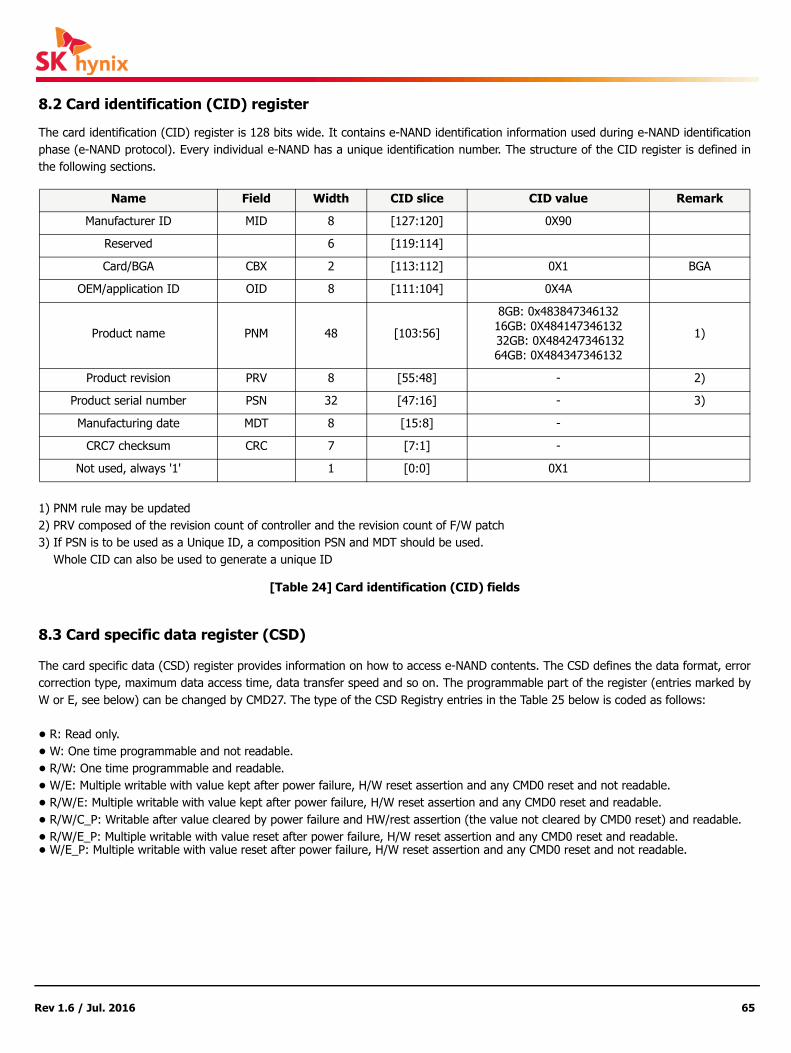
The card identification (CID) register is 128 bits wide. It contains e-NAND identification information used during e-NAND identification phase (e-NAND protocol). Every individual e-NAND has a unique identification number. The structure of the CID register is defined in the following sections.
1) PNM rule may be updated 2) PRV composed of the revision count of controller and the revision count of F/W patch3) If PSN is to be used as a Unique ID, a composition PSN and MDT should be used. Whole CID can also be used to generate a unique ID
[Table 24] Card identification (CID) fields
8.3 Card specific data register (CSD)
The card specific data (CSD) register provides information on how to access e-NAND contents. The CSD defines the data format, error correction type, maximum data access time, data transfer speed and so on. The programmable part of the register (entries marked by W or E, see below) can be changed by CMD27. The type of the CSD Registry entries in the Table 25 below is coded as follows:
• R: Read only. • W: One time programmable and not readable. • R/W: One time programmable and readable.• W/E: Multiple writable with value kept after power failure, H/W reset assertion and any CMD0 reset and not readable.• R/W/E: Multiple writable with value kept after power failure, H/W reset assertion and any CMD0 reset and readable.• R/W/C_P: Writable after value cleared by power failure and HW/rest assertion (the value not cleared by CMD0 reset) and readable.• R/W/E_P: Multiple writable with value reset after power failure, H/W reset assertion and any CMD0 reset and readable.• W/E_P: Multiple writable with value reset after power failure, H/W reset assertion and any CMD0 reset and not readable.
Name Field Width CID slice CID value Remark
Manufacturer ID MID 8 [127:120] 0X90
Reserved 6 [119:114]
Card/BGA CBX 2 [113:112] 0X1 BGA
OEM/application ID OID 8 [111:104] 0X4A
Product name PNM 48 [103:56]
8GB: 0x48384734613216GB: 0X484147346132 32GB: 0X48424734613264GB: 0X484347346132
1)
Product revision PRV 8 [55:48] - 2)
Product serial number PSN 32 [47:16] - 3)
Manufacturing date MDT 8 [15:8] -
CRC7 checksum CRC 7 [7:1] -
Not used, always '1' 1 [0:0] 0X1

Rev 1.6 / Jul. 2016 66
[Table 25]CSD fields
Name Field Width Cell type CSD slice CSD value Remark
CSD structure CSD_STRUCTURE 2 R [127:126] 0X03
System specification version SPEC_VERS 4 R [125:122] 0X04
Reserved 2 R [121:120] -
Data read access-time 1 TAAC 8 R [119:112] 0X27
Data read access-time 2 in CLKcycles (NSAC*100)
NSAC 8 R [111:104] 0X01
Max. bus clock frequency TRAN_SPEED 8 R [103:96] 0X32
Card command classes CCC 12 R [95:84] 0X8F5
Max. read data block length READ_BL_LEN 4 R [83:80] 0X09
Partial blocks for read allowed READ_BL_PARTIAL 1 R [79:79] 0X00
Write block misalignment WRITE_BLK_MISALIGN 1 R [78:78] 0X00
Read block misalignment READ_BLK_MISALIGN 1 R [77:77] 0X00
DSR implemented DSR_IMP 1 R [76:76] 0X00
Reserved 2 R [75:74] -
Device size C_SIZE 12 R [73:62] 0XFFF
Max. read current @ VDD min VDD_R_CURR_MIN 3 R [61:59] 0X07
Max. read current @ VDD max VDD_R_CURR_MAX 3 R [58:56] 0X07
Max. write current @ VDD min VDD_W_CURR_MIN 3 R [55:53] 0X07
Max. write current @ VDD max VDD_W_CURR_MAX 3 R [52:50] 0X07
Device size multiplier C_SIZE_MULT 3 R [49:47] 0X07
Erase group size ERASE_GRP_SIZE 5 R [46:42] 0X1F
Erase group size multiplier ERASE_GRP_MULT 5 R [41:37] 0X1F
Write protect group size WP_GRP_SIZE 5 R [36:32]8GB: 0x07
16/32GB : 0x0764GB: 0x0F
Write protect group enable WP_GRP_ENABLE 1 R [31:31] 0X01
Manufacturer default ECC DEFAULT_ECC 2 R [30:29] 0X00
Write speed factor R2W_FACTOR 3 R [28:26] 0X02

Rev 1.6 / Jul. 2016 67
[Table 25] CSD fields (continued)
The following sections describe the CSD fields and the relevant data types. If not explicitly defined otherwise, all bit strings are inter-preted as binary coded numbers starting with the left bit first.
Name Field Width Cell type CSD slice CSD value Remark
Max. write data block length WRITE_BL_LEN 4 R [25:22] 0X09
Partial blocks for write allowed WRITE_BL_PARTIAL 1 R [21:21] 0X00
Reserved 4 R [20:17] -
Content protection application CONTENT_PROT_APP 1 R [16:16] 0X00
File format group FILE_FORMAT_GRP 1 R/W [15:15] 0X00
Copy flag (OTP) COPY 1 R/W [14:14] 0X00
Permanent write protection PERM_WRITE_PROTECT 1 R/W [13:13] 0X00
Temporary write protection TMP_WRITE_PROTECT 1 R/W/E [12:12] 0X00
File format FILE_FORMAT 2 R/W [11:10] 0X00
ECC code ECC 2 R/W/E [9:8] 0X00
CRC CRC 7 R/W/E [7:1] -
Not used, always ‘1’ 1 [0:0] 0X01

Rev 1.6 / Jul. 2016 68
8.4 Extended CSD register
The Extended CSD register defines e-NAND properties and selected modes. It is 512 bytes long. The most significant 320 bytes are the Properties segment, which defines e-NAND capabilities and cannot be modified by the host. The lower 192 bytes are the modes segment, which defines the configuration e-NAND is working in. These modes can be changed by the host by means of the switch command.
[Table 26] Extended CSD
Name Field CSD slice Cell Type CSD value Remark
Properties segment
Reserved [511:506]
Extended Security Commands Error EXT_SECURITY_ERR [505] R 0x00
Supported command sets S_CMD_SET [504] R 0x01
HPI features HPI_FEATURES [503] R 0x01
Background operations support BKOPS_SUPPORT [502] R 0x01
Max packed read commands MAX_PACKED_READS [501] R 0x3F
Max packed write commands MAX_PACKED_WRITES [500] R 0x3F
Data Tag Support DATA_TAG_SUPPORT [499] R 0x01
Tag Unit Size TAG_UNIT_SIZE [498] R 0x00
Tag Resources Size TAG_RES_SIZE [497] R 0x00
Context management capabilities CONTEXT_CAPABILITIES [496] R 0x78
Large Unit size LARGE_UNIT_SIZE_M1 [495] R 0x01
Extended partitions attribute support EXT_SUPPORT [494] R 0x03
Supported modes SUPPORTED_MODES [493] R 0x01
FFU features FFU_FEATURES [492] R 0x00
Operation codes timeout OPERATION_CODE_TIME OUT [491] R 0x00
FFU Argument FFU_ARG [490:487] R 0xFFFAFFF0
Barrier support BARRIER_SUPPORT [486] R 0x01
Reserved [485:309] -
CMD Queuing Support CMDQ_SUPPORT [308] R 0x1
CMD Queuing Depth CMDQ_DEPTH [307] R 0x1F
Reserved [306] -
Number of FW sectors correctly programmed
NUMBER_OF_FW_SECTORS_CORRECTLY_PROGRAMMED
[305:302] R 0x00000000
Vendor proprietary health report VENDOR_PROPRIETARY_HEALTH_REPORT [301:270] R - None

Rev 1.6 / Jul. 2016 69
[Table 26] Extended CSD(Continued)
Name Field CSD slice Cell Type CSD value Remark
Device life time estimation type B DEVICE_LIFE_TIME_EST_TYP_B [269] R 0x01
Device life time estimation type A DEVICE_LIFE_TIME_EST_TYP_A [268] R 0x01
Pre EOL information PRE_EOL_INFO [267] R 0x01
Optimal read size OPTIMAL_READ_SIZE [266] R 0x40
Optimal write size OPTIMAL_WRITE_SIZE [265] R 0x40
Optimal trim unit size OPTIMAL_TRIM_UNIT_SIZE [264] R 0x07
Device version DEVICE_VERSION [263:262] R - Not fixed
Firmware version FIRMWARE_VERSION [261:254] R - Same to PRV
Power class for 200MHz, DDR at Vcc=3.6V PWR_CL_DDR_200_360 [253] R 0x22
Cache size CACHE_SIZE [252:249] R 0x0000400
Generic CMD6 timeout GENERIC_CMD6_TIME [248] R 0x05
Power off Notification (long) timeout POWER_OFF_LONG_TIME [247] R 0x64
Background operations status BKOPS_STATUS [246] R 0x00
Number of correctlyprogrammed sectors CORRECTLY_PRG_SECTORS_NUM [245:242] R - Not fixed
1st initialization time after partitioning INI_TIMEOUT_AP [241] R 0x0A
Cache Flushing Policy CACHE_FLUSH_POLICY [240] R 0x01
Power class for 52MHz, DDR at Vcc=3.6V PWR_CL_DDR_52_360 [239] R 0x11
Power class for 52MHz, DDR at Vcc=1.95V PWR_CL_DDR_52_195 [238] R 0x00 Not support
Power class for 200MHz at Vccq=1.95, Vcc=3.6V
PWR_CL_200_195 [237] R 0x22
Power class for 200MHz at Vccq=1.3, Vcc=3.6V PWR_CL_200_130 [236] R 0x00 Not support
Minimum write performancefor 8bit at 52MHz in DDR mode MIN_PERF_DDR_W_8_52 [235] R 0x78
Minimum read performancefor 8bit at 52MHz in DDR mode
MIN_PERF_DDR_R_8_52 [234] R 0x8C
Reserved [233]
TRIM multiplier TRIM_MULT [232] R 0x02
Secure feature support SEC_FEATURE_SUPPORT [231] R 0x55
Secure erase multiplier SEC_ERASE_MULT [230] R8GB : 0x1916GB : 0x32
32/64GB : 0x64
Secure TRIM multiplier SEC_TRIM_MULT [229] R 0x0A

Rev 1.6 / Jul. 2016 70
[Table 26] Extended CSD(Continued)
Name Field CSD slice Cell Type CSD value Remark
Boot information BOOT_INFO [228] R 0x07
Reserved [227] -
Boot partition size BOOT_SIZE_MULTI [226] R 0x20
Access size ACC_SIZE [225] R 0x06
High-capacity erase unit size HC_ERASE_GRP_SIZE [224] R 0x01
High-capacity erase timeout ERASE_TIMEOUT_MULT [223] R 0x02
Reliable write sector count REL_WR_SEC_C [222] R 0x01
High-capacity write protect group size HC_WP_GRP_SIZE [221] R8GB : 0x08
16/32GB : 0x0864GB : 0x10
Sleep current(Vcc) S_C_Vcc [220] R 0x07
Sleep current(Vccq) S_C_Vccq [219] R 0x07
Production state awareness timeoutPRODUCTION_STATE_AWARENES S_TIMEOUT [218] R 0x00
Sleep/awake timeout S_A_TIMEOUT [217] R 0x11
Sleep Notification Timeout SLEEP_NOTIFICATION_TIME [216] R 0x0C
Sector count SEC_COUNT [215:212] R
8GB: 0xE9000016GB: 0X1D5A00032GB: 0X03A3E00064GB: 0X747C000
Secure Write Protect information SECURE_WP_INFO [211] R 0x01
Minimum write performancefor 8bit at52MHz MIN_PERF_W_8_52 [210] R 0x8C
Minimum read performancefor 8bit at 52MHz
MIN_PERF_R_8_52 [209] R 0x8C
Minimum write performancefor 8bit at 26MHz, for 4bit at 52MHz MIN_PERF_W_8_26_4_52 [208] R 0x46
Minimum read performancefor 8bit at 26MHz, for 4bit at 52MHz MIN_PERF_R_8_26_4_52 [207] R 0x46
Minimum write performancefor 4bit at 26MHz
MIN_PERF_W_4_26 [206] R 0x1E
Minimum read performancefor 4bit at 26MHz MIN_PERF_R_4_26 [205] R 0x1E
Reserved [204]
Power class for 26MHz at 3.6V PWR_CL_26_360 [203] R 0x00
Power class for 52MHz at 3.6V PWR_CL_52_360 [202] R 0x00
Power class for 26MHz at 1.95V PWR_CL_26_195 [201] R 0x00 Not support
Power class for 52MHz at 1.95V PWR_CL_52_195 [200] R 0x00 Not support

Rev 1.6 / Jul. 2016 71
[Table 26] Extended CSD(Continued)
Name Field CSD slice Cell Type CSD value Remark
Partition switching timing PARTITION_SWITCH_TIME [199] R 0x01
Out-of-interrupt busy timing OUT_OF_INTERRUPT_TIME [198] R 0x05
I/O Driver Strength DRIVER_STRENGTH [197] R 0x1F
Device type DEVICE_TYPE [196] R 0x57
Reserved [195] -
CSD structure CSD_STRUCTURE [194] R 0x02
Reserved [193] -
Extended CSD revision EXT_CSD_REV [192] R 0x08
Modes Segment
Command set CMD_SET [191] R/W/E_P 0x00
Reserved [190] -
Command set revision CMD_SET_REV [189] R 0x00
Reserved [188] -
Power class POWER_CLASS [187] R/W/E_P 0x00
Reserved [186] -
High-speed interface timing HS_TIMING [185] R/W/E_P 0x00
Strobe Support STROBE_SUPPORT [184] R 0x01
Bus width mode BUS_WIDTH [183] W/E_P 0x00
Reserved [182] -
Erased memory content ERASED_MEM_CONT [181] R 0x00
Reserved [180] -
Partition configuration PARTITION_CONFIG [179] R/W/E &R/W/E_P 0x00
Boot config protection BOOT_CONFIG_PROT [178] R/W/E &R/W/C_P
0x00
Boot bus conditions BOOT_BUS_CONDITIONS [177] R/W/E 0x00
Reserved [176] -
High-density erase group definition ERASE_GROUP_DEF [175] R/W/E_P 0x00
Boot write protection status registers BOOT_WP_STATUS [174] R 0x00
Boot area write protection register BOOT_WP [173] R/W/E &R/W/C_P
0x00
Reserved [172] -

Rev 1.6 / Jul. 2016 72
[Table 26] Extended CSD(Continued)
Name Field CSD slice Cell Type CSD value Remark
User area write protection register USER_WP [171]R/W, R/W/C_P & /W/
E_P0x00
Reserved [170] -
FW configuration FW_CONFIG [169] R/W 0x00
RPMB Size RPMB_SIZE_MULT [168] R 0x20
Write reliability setting register WR_REL_SET [167] R/W 0x1F
Write reliability parameter register WR_REL_PARAM [166] R 0x15
Sanitize start SANITIZE_START [165] W/E_P 0x00
Manually start background operations BKOPS_START [164] W/E_P 0x00
Enable background operations Handshake
BKOPS_EN [163] R/W 0x00
H/W reset function RST_n_FUNCTION [162] R/W 0x00
HPI management HPI_MGMT [161] R/W/E_P 0x00
Partitioning support PARTITIONING_SUPPORT [160] R 0x07
Max enhanced area size MAX_ENH_SIZE_MULT [159:157] R
8GB: 0x0003A416GB: 0X00075632GB: 0X000E8F64GB: 0X000E8F
Partitions attribute PARTITIONS_ATTRIBUTE [156] R/W 0x00
Partitioning setting PARTITION_SETTING_COMPLETED [155] R/W 0x00
General purpose partition size GP_SIZE_MULT [154:143] R/W 0x00
Enhanced user data area size ENH_SIZE_MULT [142:140] R/W 0x00
Enhanced user data start address ENH_START_ADDR [139:136] R/W 0x00
Reserved [135] -
Bad Block management mode SEC_BAD_BLK_MGMNT [134] R/W 0x00
Production state awareness PRODUCTION_STATE_AWARENESS [133] R/W/E -
Package Case Temperature is Controlled TCASE_SUPPORT [132] W/E_P 0x00
Periodic Wake-up PERIODIC_WAKEUP [131] R/W/E 0x00
Program CID/CSD in DDR mode support PROGRAM_CID_CSD_DDR_SUPPORT [130] R 0x00
Reserved [129:128] -
Vendor Specific Fields VENDOR_SPECIFIC_FIELD [127:64]Vendor specific -
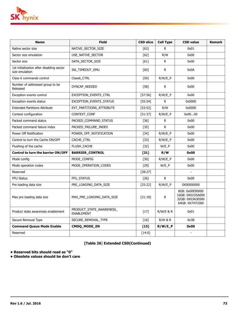
Rev 1.6 / Jul. 2016 73
[Table 26] Extended CSD(Continued)
• Reserved bits should read as “0”• Obsolete values should be don’t care
Name Field CSD slice Cell Type CSD value Remark
Native sector size NATIVE_SECTOR_SIZE [63] R 0x01
Sector size emulation USE_NATIVE_SECTOR [62] R/W 0x00
Sector size DATA_SECTOR_SIZE [61] R 0x00
1st initialization after disabling sector size emulation INI_TIMEOUT_EMU [60] R 0x0A
Class 6 commands control Class6_CTRL [59] R/W/E_P 0x00
Number of addressed group to be Released DYNCAP_NEEDED [58] R 0x00
Exception events control EXCEPTION_EVENTS_CTRL [57:56] R/W/E_P 0x00
Exception events status EXCEPTION_EVENTS_STATUS [55:54] R 0x0000
Extended Partitions Attribute EXT_PARTITIONS_ATTRIBUTE [53:52] R/W 0x0000
Context configuration CONTEXT_CONF [51:37] R/W/E_P 0x00...00
Packed command status PACKED_COMMAND_STATUS [36] R 0x00
Packed command failure index PACKED_FAILURE_INDEX [35] R 0x00
Power Off Notification POWER_OFF_NOTIFICATION [34] R/W/E_P 0x00
Control to turn the Cache ON/OFF CACHE_CTRL [33] R/W/E_P 0x00
Flushing of the cache FLUSH_CACHE [32] W/E_P 0x00
Control to turn the barrier ON/OFF BARRIER_CONTROL [31] R/W 0x00
Mode config MODE_CONFIG [30] R/W/E_P 0x00
Mode operation codes MODE_OPERATION_CODES [29] W/E_P 0x00
Reserved [28:27] -
FFU Status FFU_STATUS [26] R 0x00
Pre loading data size PRE_LOADING_DATA_SIZE [25:22] R/W/E_P 0X00000000
Max pre loading data size MAX_PRE_LOADING_DATA_SIZE [21:18] R
8GB: 0x00E9000016GB: 0X01D5A00032GB: 0X03A3E00064GB: 0X747C000
Product state awareness enablement PRODUCT_STATE_AWARENESS_ENABLEMENT [17] R/W/E & R 0x01
Secure Removal Type SECURE_REMOVAL_TYPE [16] R/W & R 0x3B
Command Queue Mode Enable CMDQ_MODE_EN [15] R/W/E_P 0x00
Reserved [14:0] -

Rev 1.6 / Jul. 2016 74
8.5 RCA (Relative card address)
The writable 16-bit relative card address (RCA) register carries the card address assigned by the host during the card identification. This address is used for the addressed host-card communication after the card identification procedure. The default value of the RCA register is 0x0001. The value 0x0000 is reserved to set all cards into the Stand-by State with CMD7.
8.6 DSR (Driver stage register)
It can be optionally used to improve the bus performance for extended operating conditions (depending on parameters like bus length, transfer rate or number of Devices). The CSD register carries the information about the DSR register usage. The default value of the
DSR register is 0x404.