SiP’s Role in Enabling the Internet of Everything: What ... · PDF fileSiP’s Role...
23
© 2015 TechSearch International, Inc. www.techsearchinc .com SiP’s Role in Enabling the Internet of Everything: What Format Will it Be? E. Jan Vardaman, President and Founder, TechSearch International
Transcript of SiP’s Role in Enabling the Internet of Everything: What ... · PDF fileSiP’s Role...

© 2015 TechSearch International, Inc. w w w . t e c h s e a r c h i n c. c o m
SiP’s Role in Enabling the Internet of Everything: What Format Will it Be?
E. Jan Vardaman, President and Founder, TechSearch International

© 2015 TechSearch International, Inc. w w w . t e c h s e a r c h i n c . c om
Connected Device Market: It’s Growing
• Market growth for connected devices according to Cisco • Morgan Stanley wearable electronics growth rate of 154% • Shipments projected to increase from 6 million units in 2013 to 248
million units in 2017
© 2015 TechSearch International, Inc. w w w . t e c h s e a r c h i n c . c om
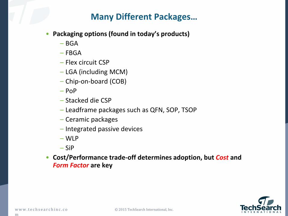
Many Different Packages…
• Packaging options (found in today’s products) – BGA – FBGA – Flex circuit CSP – LGA (including MCM) – Chip-on-board (COB) – PoP – Stacked die CSP – Leadframe packages such as QFN, SOP, TSOP – Ceramic packages – Integrated passive devices – WLP – SiP
• Cost/Performance trade-off determines adoption, but Cost and Form Factor are key

© 2015 TechSearch International, Inc. w w w . t e c h s e a r c h i n c . c om
Internet of Everything
Source: Cisco.

© 2015 TechSearch International, Inc. w w w . t e c h s e a r c h i n c . c om
Many Wrist Products
• Health and fitness tracking bands • Watch products • Contain many sensors to accurately calculate
– Heart rate – Blood pressure (need higher accuracy) and
blood flow – Glucose levels – Pulse, motion sensing, etc.
• But, sensors have to function properly!! – Many examples of heart rate or blood
pressure sensors that don’t measure accurately
– Limits product adoption: “Users will stop using the devices and enterprises will not adopt the technology if data is not accurate” according to Morgan Stanley survey
Source: Apple.

© 2015 TechSearch International, Inc. w w w . t e c h s e a r c h i n c . c om
Low-Power Optimized MCU for Fitness Band
• Design is key • Trade-off in design is power vs. performance • Processor is constantly analyzing data from sensor
© 2015 TechSearch International, Inc. w w w . t e c h s e a r c h i n c . c om
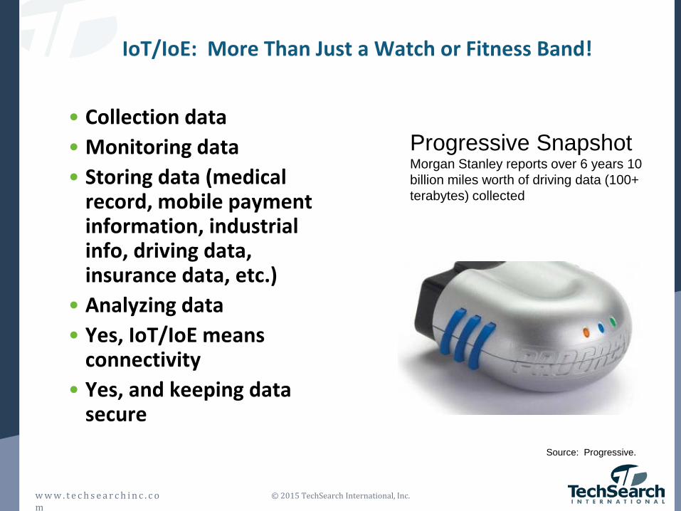
IoT/IoE: More Than Just a Watch or Fitness Band!
• Collection data • Monitoring data • Storing data (medical
record, mobile payment information, industrial info, driving data, insurance data, etc.)
• Analyzing data • Yes, IoT/IoE means
connectivity • Yes, and keeping data
secure
Source: Progressive.
Progressive Snapshot Morgan Stanley reports over 6 years 10 billion miles worth of driving data (100+ terabytes) collected

© 2015 TechSearch International, Inc. w w w . t e c h s e a r c h i n c . c om
Automotive Driver Assistance
• Many safety features for automotive
– Sensor technology to collect and process information
• SiP used for radar modules – FO-WLP format (Freescale,
Infineon, NXP) • SiP for other sensor modules
Source: Freescale. Source: NXP.

© 2015 TechSearch International, Inc. w w w . t e c h s e a r c h i n c . c om
Smartphones Control Connected Devices
• Smartphones are part of IoE – Tool with use of sensors – Pressure on package design
• Medical products using signal to smart phone for monitoring
– Body conditions (blood pressure, heart rate, glucose level, etc.) using sensors
– Medicine consumption • Home security
– Wireless sensors located in house – Controlled by smartphone (in my case
iPhone) • Energy monitoring
– Thermostat with wireless sensor – Change settings remotely with
smartphone – Monitor energy consumption providing
data for analysis on usage
© 2015 TechSearch International, Inc. w w w . t e c h s e a r c h i n c . c om
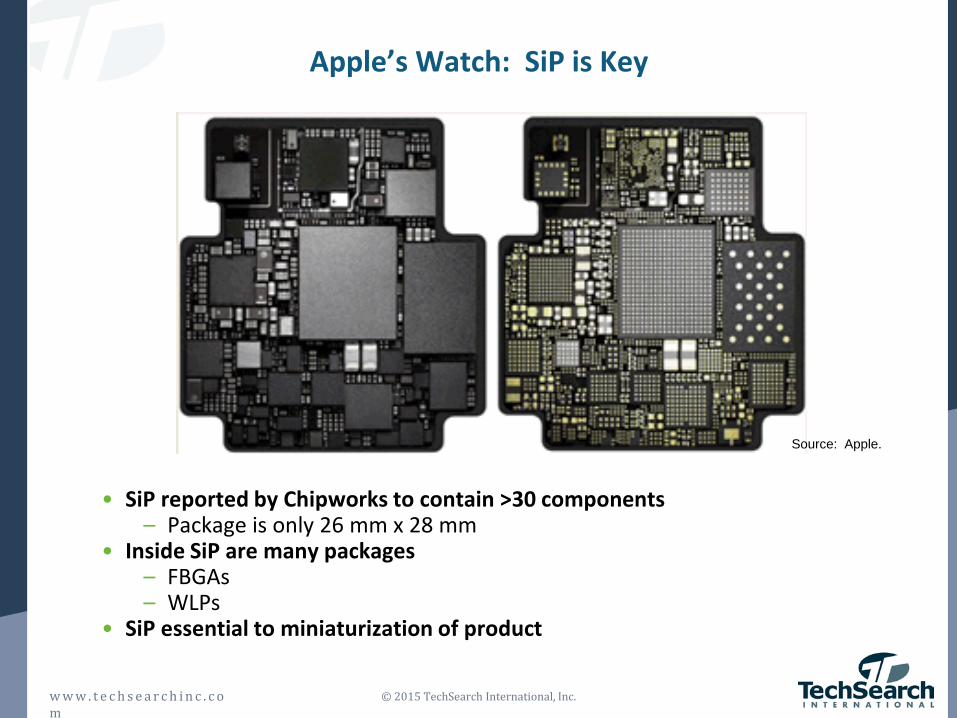
Apple’s Watch: SiP is Key
• SiP reported by Chipworks to contain >30 components – Package is only 26 mm x 28 mm
• Inside SiP are many packages – FBGAs – WLPs
• SiP essential to miniaturization of product
Source: Apple.

© 2015 TechSearch International, Inc. w w w . t e c h s e a r c h i n c . c om
System-in-Package: Key to Connected Devices
• Renesas and Link Labs radio module for machine-to-machine communication
– Renesas microcontroller – Semtech long distance radio
transceiver – Applications including security
monitoring, agricultural monitoring, home automation, smart meters
• Samsung Electronics Artik modules – Contains processors, memory,
communication chips, and software – All essential elements for connected
gadgets
Source: Samsung.

© 2015 TechSearch International, Inc. w w w . t e c h s e a r c h i n c . c om
How Do We Define SiP?
• Package containing combination of two or more dissimilar die
– May include MEMS assembled into a single package
• Typically combined with other components such as
– Passives – Filters – Antennas
• Some companies define as single die with integrate passive devices (stand alone or embedded)
– If it functions as a system or sub-system
• Single die with pre-packaged die on a substrate of a package
• More than one IC with different functionality in a single package
Source: TPSS.

© 2015 TechSearch International, Inc. w w w . t e c h s e a r c h i n c . c om
SiP May Include…Can be in Many Formats…
• Power amplifier module (PA or PAM) • Front end module (FEM) • RF module • Transceiver + RF frontend • SSD (with controller, NAND memory,
and power source) • Antenna Switches / Frontend Module
& Transceiver • Connectivity Modules • Power Management Module • MEMS integration with ASIC (this
could be stacked in a QFN) • 3G/4G Modem
LGA module
BGA
FO-WLP
PoP
Routable QFN

© 2015 TechSearch International, Inc. w w w . t e c h s e a r c h i n c . c om
• 2 Layer-RDL Interconnection • 2 Active Die + 10 Passives 0201 SMD
After Molding
After Pick & Place
After Thin Film Processing, Solder Ball Attach and Singulation
FO-WLP SiP Solution
Source: NANIUM
© 2015 TechSearch International, Inc. w w w . t e c h s e a r c h i n c . c om
FO-WLP Merchant Suppliers Status
• Amkor Technology redeploying FO-WLP with new 300mm line (eWLB) in K4 plant
• ADL Engineering 200mm pilot line in Taiwan • ASE license for Infineon’s eWLB with 300mm
in Taiwan, also offers “chip last” panel version
• Deca Technologies (300mm “panel” format) • Huatian-FCI/Fujikura (embedded WLP in flex
circuit) • J-Devices (embedded die in laminate) • NANIUM (300mm wafer) license for
Infineon’s eWLB • NEPES (300mm line in Korea) based on
Freescale’s RCP process • PTI (R&D on panel) • SPIL (300mm wafer) • STATS ChipPAC (300mm wafer) will be
purchased by JCET, license for Infineon’s eWLB
• TSMC (300mm wafer InFO WLP) • New suppliers TBD
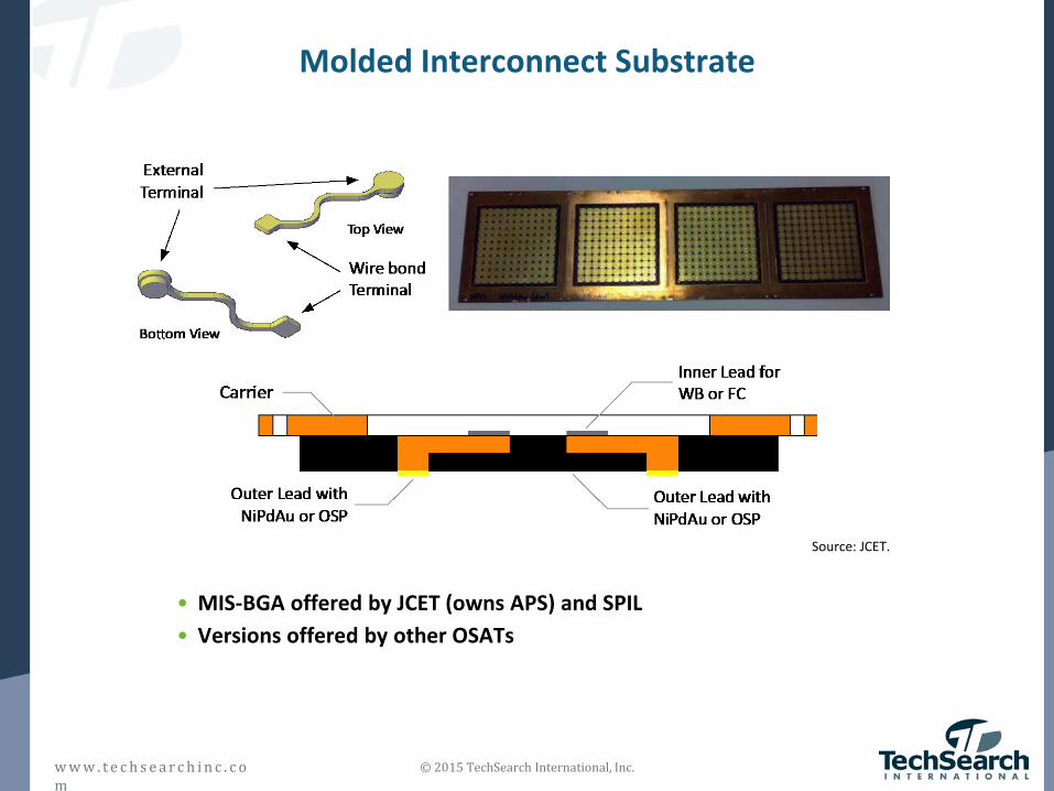
© 2015 TechSearch International, Inc. w w w . t e c h s e a r c h i n c . c om
Molded Interconnect Substrate
• MIS-BGA offered by JCET (owns APS) and SPIL • Versions offered by other OSATs
Source: JCET.

© 2015 TechSearch International, Inc. w w w . t e c h s e a r c h i n c . c om
Routable QFN Including MIS
• Molded interconnect substrate (MIS) or coreless substrate packages – Based on a modified leadframe technology – Leadframe is molded before die attach – Wire bond or Cu pillar flip chip interconnect – Multiple die possible – Baseband processors and connectivity devices targeting this
• Routable QFNs – Routable package allows area under die to be used, provides easy saw
singulation, is strip testable, and can be used as a multi-die solution – Many OSATs offering versions of routable QFNs today – Multiple die possible
Source: Amkor Technology.
Source: UTAC.
Bottom View Cross section view
Substrate
Mold
Die
Solder ball

© 2015 TechSearch International, Inc. w w w . t e c h s e a r c h i n c . c om
SPIL’s FC-MISBGA Package (Flip Chip – Molded Interconnect System BGA)
• Coreless substrate (no copper clad laminate core) • Embedded trace technology: better trace adhesion to substrate dielectric
layer • Fine trace: L/S=20/20µm, 15/15µm trace formed by embedded trace
technology, not SAP • Molding compound replaces prepreg • Trace routability • Little warpage • Excellent electrical performance • Good thermal and reliability performance
Source: SPIL.

© 2015 TechSearch International, Inc. w w w . t e c h s e a r c h i n c . c om
ASE’s Chip Last Process as SiP
• Uses low-cost coreless substrate – Fine pitch capable (15µm L/S, 12µm L/S in development) – Manufactured in double panel format – Assembled in strip format – Multi-die and passives possible – Can be bottom PoP
• Thin package (<375 µm) • High current and thermal handling capabilities
– Due to thicker Cu (15-20 µm) • Uses existing FC infrastructure
– Flip chip with Cu pillar mounted on coreless substrate – Mass reflow and molded underfill
Source: ASE.
Multi-Die Coreless “Chip Last” Package

© 2015 TechSearch International, Inc. w w w . t e c h s e a r c h i n c . c om
Embedded Die SiP Options
• Embedded die formats – Embedded active die (application
processor) in bottom laminate substrate – Fan-out WLP with application processor
as bottom package • Embedded die examples
– RF modules for mobile and other applications
– Power management modules for mobile and other applications
– Battery management modules Source: TDK.

© 2015 TechSearch International, Inc. w w w . t e c h s e a r c h i n c . c om
Who Will Assemble SiP?
• OSAT – Familiar with design tools for modules/packages, including electrical
and thermal modeling, antenna design – History of obtaining die from many sources – Capability of fine pitch wire bond or flip chip – Capable of providing required EMI shielding (critical for some modules) – Package test capability
• EMS – Good ability to purchase materials (infrastructure), driven by low
margins of business – Provided components from multiple sources – High throughput SMT machines capable of die and passive device
placement – Panel process capability, could do embedded die

© 2015 TechSearch International, Inc. w w w . t e c h s e a r c h i n c . c om
Conclusions
• SiP is an enabler of many products for the trend in connectivity • Demand for lower cost solutions drives adoption of new package designs
– No single format (Laminate substrate, FO-WLP, Leadframe package, etc.)
– No “one size fits all” solution, but economics and business considerations will drive package adoption
– Package selection important: Can’t stretch the selected package option past its capability (rubber band theory)
• Industry needs to develop consensus on SiP definition • Industry is still determining who will play the major roles in assembly:
OSAT or EMS • Or will foundry do the SiP?????

© 2015 TechSearch International, Inc. w w w . t e c h s e a r c h i n c. c o m
Thank you!
TechSearch International, Inc. 4801 Spicewood Springs Road, Suite 150
Austin, Texas 78759 USA +1.512.372.8887