SINUSOIDAL STEADY STATE ANALYSISocw.nthu.edu.tw/ocw/upload/12/241/09handout.pdf · SINUSOIDAL...
45
1 C.T. Pan C.T. Pan 1 SINUSOIDAL STEADY SINUSOIDAL STEADY STATE ANALYSIS STATE ANALYSIS 2 C.T. Pan C.T. Pan 9.1 Sinusoidal Source 9.1 Sinusoidal Source 9.2 Phasors 9.2 Phasors 9.3 Kirchhoff 9.3 Kirchhoff’ s Laws in the Frequency Domain s Laws in the Frequency Domain 9.4 Component Models in Phasor Domain 9.4 Component Models in Phasor Domain 9.5 Series, Parallel, and Delta 9.5 Series, Parallel, and Delta- to to- Wye Wye simplifications simplifications 2
Transcript of SINUSOIDAL STEADY STATE ANALYSISocw.nthu.edu.tw/ocw/upload/12/241/09handout.pdf · SINUSOIDAL...

11C.T. PanC.T. Pan 11
SINUSOIDAL STEADY SINUSOIDAL STEADY
STATE ANALYSIS STATE ANALYSIS
22C.T. PanC.T. Pan
9.1 Sinusoidal Source9.1 Sinusoidal Source
9.2 Phasors9.2 Phasors
9.3 Kirchhoff9.3 Kirchhoff’’s Laws in the Frequency Domains Laws in the Frequency Domain
9.4 Component Models in Phasor Domain9.4 Component Models in Phasor Domain
9.5 Series, Parallel, and Delta9.5 Series, Parallel, and Delta--toto--Wye Wye simplificationssimplifications
22
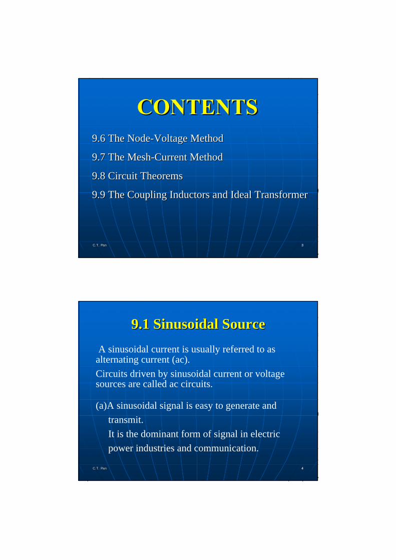
33C.T. PanC.T. Pan
9.6 The Node9.6 The Node--Voltage MethodVoltage Method
9.7 The Mesh9.7 The Mesh--Current MethodCurrent Method
9.8 Circuit Theorems9.8 Circuit Theorems
9.9 The Coupling Inductors and Ideal Transformer9.9 The Coupling Inductors and Ideal Transformer
33
A sinusoidal current is usually referred to as alternating current (ac). Circuits driven by sinusoidal current or voltage sources are called ac circuits.
(a)A sinusoidal signal is easy to generate and transmit.It is the dominant form of signal in electric power industries and communication.
44C.T. PanC.T. Pan 44
9.1 Sinusoidal Source 9.1 Sinusoidal Source
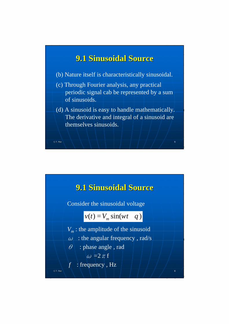
(b) Nature itself is characteristically sinusoidal.
(c) Through Fourier analysis, any practical periodic signal cab be represented by a sum of sinusoids.
(d) A sinusoid is easy to handle mathematically. The derivative and integral of a sinusoid are themselves sinusoids.
55C.T. PanC.T. Pan 55
9.1 Sinusoidal Source 9.1 Sinusoidal Source
Consider the sinusoidal voltage
66C.T. PanC.T. Pan 66
9.1 Sinusoidal Source 9.1 Sinusoidal Source
( ) sin( )mv t V tω θ= +
Vm : the amplitude of the sinusoid ω : the angular frequency , rad/sθ : phase angle , rad
ω =2πff : frequency , Hz
77C.T. PanC.T. Pan 77
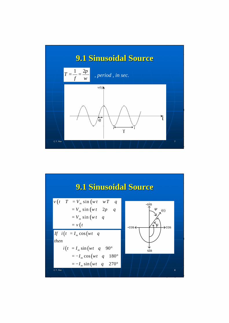
9.1 Sinusoidal Source 9.1 Sinusoidal Source 1 2Tf
πω
= = , period , in sec.
88C.T. PanC.T. Pan 88
9.1 Sinusoidal Source 9.1 Sinusoidal Source ( ) ( )
( )( )
( )
sin
sin 2
sin
m
m
m
v t T V t T
V t
V t
v t
ω ω θ
ω π θ
ω θ
+ = + +
= + +
= +
=
( ) ( )
( ) ( )( )( )
cos
sin 90
cos 180
sin 270
m
m
m
m
If i t I tthen
i t I t
I t
I t
ω θ
ω θ
ω θ
ω θ
= +
= + + °
= − + + °
= − + + °
cos
-sin
-cos
sin
i(t)
θ
ψ
99C.T. PanC.T. Pan 99
9.1 Sinusoidal Source 9.1 Sinusoidal Source
cos
-sin
-cos
sin
i(t)
θ
ψsin
cos
sin
cos
om
om
om
om
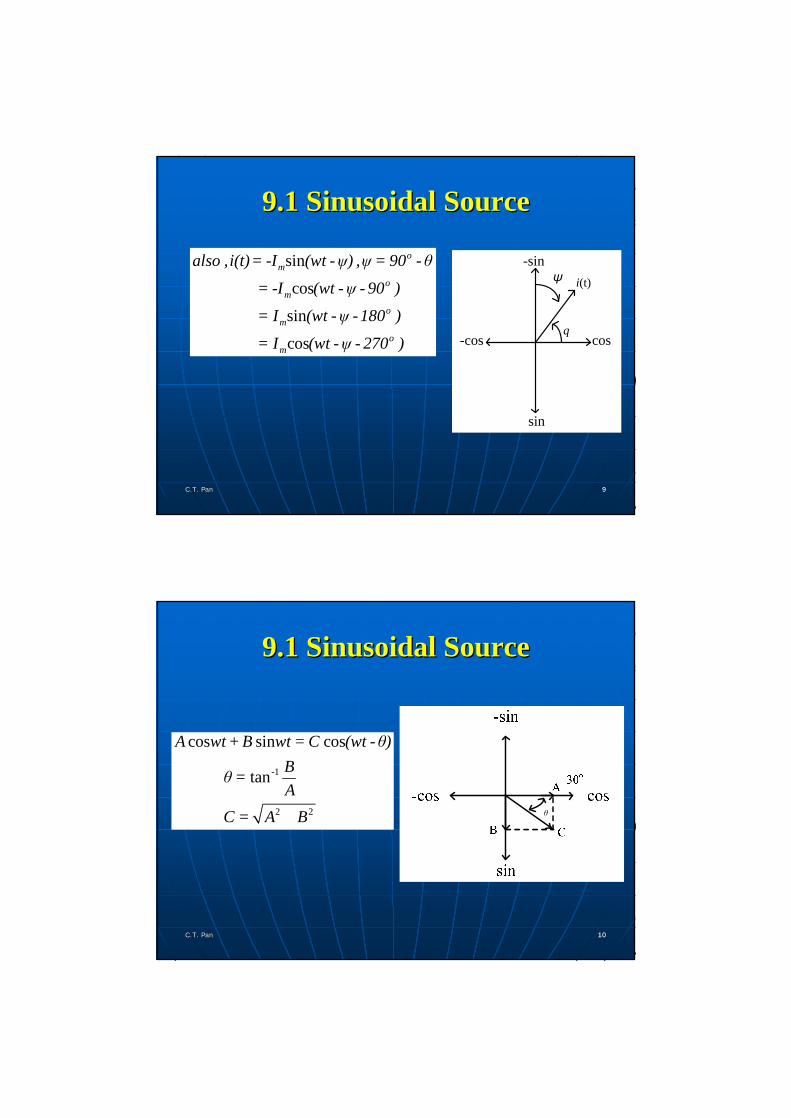
also , i(t)= -I (wt -ψ) , ψ= 90 -θ = -I (wt -ψ - 90 ) = I (wt -ψ -180 ) = I (wt -ψ - 270 )
1010C.T. PanC.T. Pan 1010
9.1 Sinusoidal Source 9.1 Sinusoidal Source
-1
2 2
cos sin cos
tan
A wt + B wt = C (wt -θ)B θ=A
C A B= + θ
1111C.T. PanC.T. Pan 1111
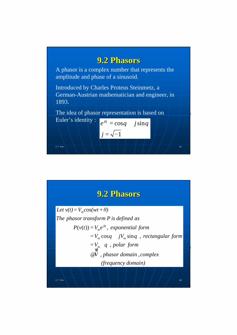
9.2 Phasors 9.2 Phasors A phasor is a complex number that represents the amplitude and phase of a sinusoid.
Introduced by Charles Proteus Steinmetz, a German-Austrian mathematician and engineer, in 1893.
The idea of phasor representation is based on Euler’s identity : cos sin
1
je j
j
θ θ θ= +
= −
1212C.T. PanC.T. Pan 1212
9.2 Phasors 9.2 Phasors
( ( )) , cos sin , ,
m
jm
m m
m
Let v(t)=V cos(wt +θ)The phasor transform P is defined as
P v t V e exponential formV jV rectangular formV polar form
θ
θ θ
θ
=
= +
= ∠
, V phasor domain , complex (frequency domain)
ur@

1313C.T. PanC.T. Pan 1313
9.2 Phasors 9.2 Phasors
It is assumed that the angular frequency is known.
1 ( ) Re[ ] Re[ ] cos( ) ( ) ,
jwt
j jwtm
m
The inverse phasor transform is defined as
P V VeV e e
V wtv t time domain , real
θ
θ
− =
=
= +
=
ur ur
value
100 30oV V= ∠ur
50 20I A°= ∠ −r
1414C.T. PanC.T. Pan 1414
9.2 Phasors 9.2 Phasors Example :( ) 100cos( 30 )V( ) 50sin( 70 )A
The phasor diagram is as follows :
o
o
v t wti t wt
= +
= +
o
o
Phasor leads by 50
Phasor lags by 50
V I
I V
uur r
r uur
A convention used in power systems is as follows:
The electric load is lagging, which means the load current phasor lags the voltage phasor.
1515C.T. PanC.T. Pan 1515
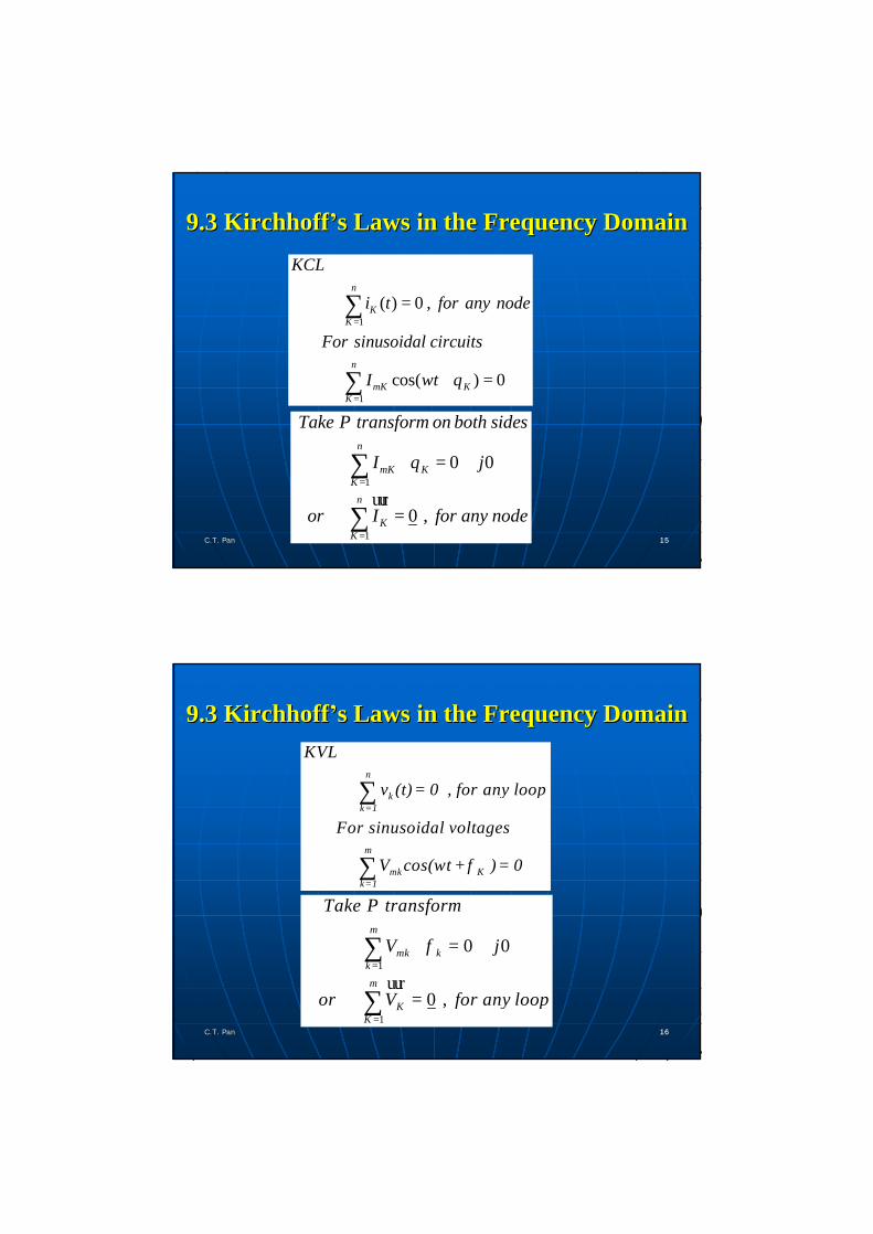
9.3 Kirchhoff9.3 Kirchhoff’’s Laws in the Frequency Domains Laws in the Frequency Domain
1
1
( ) 0 ,
cos( ) 0
n
KK
n
mK KK
KCL
i t for any node
For sinusoidal circuits
I wt θ
=
=
=
+ =
∑
∑
1
1
0 0
0 ,
n
mK KK
n
KK
Take P transform on both sides
I j
or I for any node
θ=
=
∠ = +
=
∑
∑uur
1616C.T. PanC.T. Pan 1616
9.3 Kirchhoff9.3 Kirchhoff’’s Laws in the Frequency Domains Laws in the Frequency Domain
n
kk=1
m
mk Kk=1
KVL
v (t)= 0 , for any loop
For sinusoidal voltages
V cos(wt + )= 0φ
∑
∑
1
1
0 0
0 ,
m
mk kkm
KK
Take P transform
V j
or V for any loop
φ=
=
∠ = +
=
∑
∑uur
1717C.T. PanC.T. Pan 1717
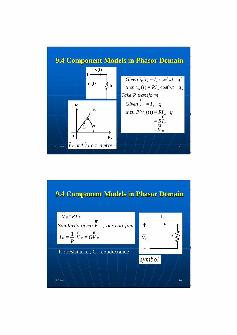
9.4 Component Models in Phasor Domain9.4 Component Models in Phasor Domain
R
( ) cos( ) ( ) cos( )
( ( )) =
=
R m
m
R m
R m
R
R
Given i t I wtthen v t RI wt
Take P transform
Given I Ithen P v t RI
RI
V
θ
θ
θθ
= +
= +
= ∠∠
=
r
r
ur
RRV and I are in phase.ur r
RVur
RIr
1818C.T. PanC.T. Pan 1818
9.4 Component Models in Phasor Domain9.4 Component Models in Phasor Domain
VR
IR
R
=
, 1
RR
R
R R R
V RI
Similarity given V one can find
I V GVR
∴
= =
ur r
ur
r ur ur
R : resistance , G : conductance symbol
1919C.T. PanC.T. Pan 1919
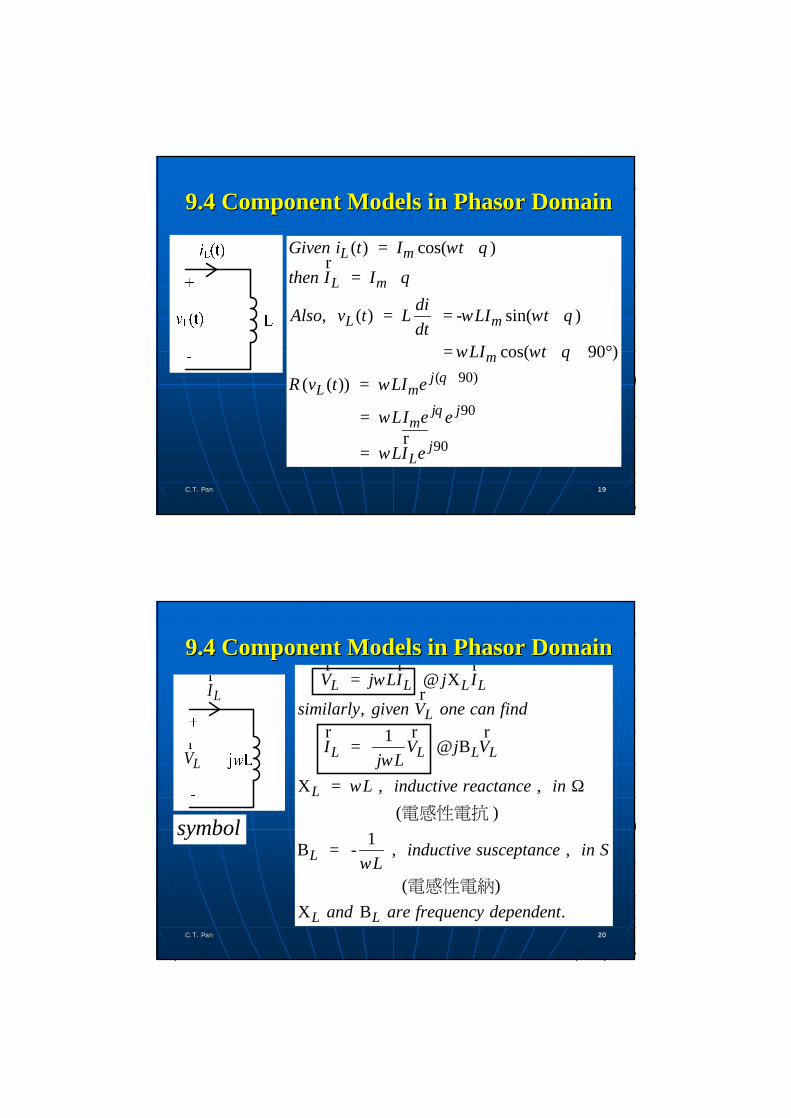
9.4 Component Models in Phasor Domain9.4 Component Models in Phasor Domain
( 90)
90
( ) cos( )
, ( ) - sin( )
cos( 90 )
( ( ))
L m
L m
L m
mj
L mj j
m
Given i t I t
then I IdiAlso v t L LI tdt
LI t
v t LI e
LI e e
LI
θ
θ
ω θ
θ
ω ω θ
ω ω θ
Ρ ω
ω
ω
+
= +
= ∠
= = +
= + + °
=
=
=
r
r 90jLe
2020C.T. PanC.T. Pan 2020
9.4 Component Models in Phasor Domain9.4 Component Models in Phasor Domain
LVr
LIr
, 1
, , ( )
1 - , ,
( )
L L L L
L
L L L L
L
L
L L
V j LI j I
similarly given V one can find
I V j Vj L
L inductive reactance in
inductive susceptance in SL
and are frequenc
ω
ωω
ω
∴ = Χ
= Β
Χ = Ω
Β =
Χ Β
r r r@r
r r r@
電感性電抗
電感性電納
.y dependent
symbol
2121C.T. PanC.T. Pan 2121
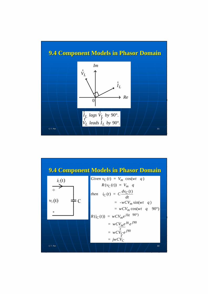
9.4 Component Models in Phasor Domain9.4 Component Models in Phasor Domain
Re
Im
LVr
LIr
0
90 .
90 .L L
L L
I lags V by
V leads I by
°
°
r r
r r
2222C.T. PanC.T. Pan 2222
9.4 Component Models in Phasor Domain9.4 Component Models in Phasor Domain
( 90 )
( ) cos( ) ( ( ))
( ) ( )
- sin( ) cos( 90 )
( ( ))
C m
C m
CC
m
mj
C mj
m
Given v t V tv t V
dv tthen i t CdtCV t
CV t
i t CV e
CV e
θ
ω θ
Ρ θ
ω ω θ
ω ω θ
Ρ ω
ω
+ °
= +
= ∠
=
= +
= + + °
=
= 90
90
j
jC
C
e
CV e
j CV
θ
ω
ω
=
=
r
r
2323C.T. PanC.T. Pan 2323
9.4 Component Models in Phasor Domain9.4 Component Models in Phasor Domain
C
C
C
,
1 XC
, , ( )
1 - , ,
( )
C C C C
C C C
C C
I j CV j Vsimilarly one can get
V I j Ij
C capacitive susceptance in S
capacitive reactance inC
and are frequency dependent
ω
ωω
ω
∴ = Β
=
Β =
Χ = Ω
Β Χ
r r r@
r r r@
電容性電納
電容性電抗
.
90 .
90 .C C
C C
I leads V by
V lags I by
°
°
r r
r r
Re
Im
CIr
CVr
9.4 Component Models in Phasor Domain9.4 Component Models in Phasor Domain
Summary of the component modelsElement Time domain Frequency domain
R
L
C
v Rii Gv
==
0
1(0)t
div Ldt
i i vdtL
=
= + ∫
01(0)
tv v idt
Cdvi Cdt
= +
=
∫
V RII GV
=
=
r rr r
j1
j L
V LI
I V
ω
ω
=
=
r r
r r
1V Ij C
I j CVω
ω
=
=
r r
r r
9.4 Component Models in Phasor Domain9.4 Component Models in Phasor Domain
From the above phasor domain models of the R, L, C elements, the ratio of the phasor voltage to the phasor current.
, ,
1 ,
R for resistorV j L for inductorI
j for capacitorC
ω
ω
= −
rr
, , VLet Z impedance inI
Ωrr @
The impedance represents the opposition that the circuit exhibits to the flow of sinusoidal current. It is a complex quantity. It is not a phasor.
9.4 Component Models in Phasor Domain9.4 Component Models in Phasor Domain
The impedance can be expressed in rectangular form or polar form as
2 2
-1
tan
R= cos , X= sin
Z R jX Z
Z R XXR
Z Z
θ
θ
θ θ
+ ∠
= +
=
@ A
9.4 Component Models in Phasor Domain9.4 Component Models in Phasor Domain
R電阻 , X電抗 ,Z 阻抗
Definition
1
Re , , Im , ,
: ,
IY G jBZV
G Y conductance SB Y susceptance SY admittance in S
= = +
==
rr@
電導 電納 導納G : , B : , Y :
9.4 Component Models in Phasor Domain9.4 Component Models in Phasor Domain
,'
V Z I I YVcomplex ohm s law
= =ur r r ur
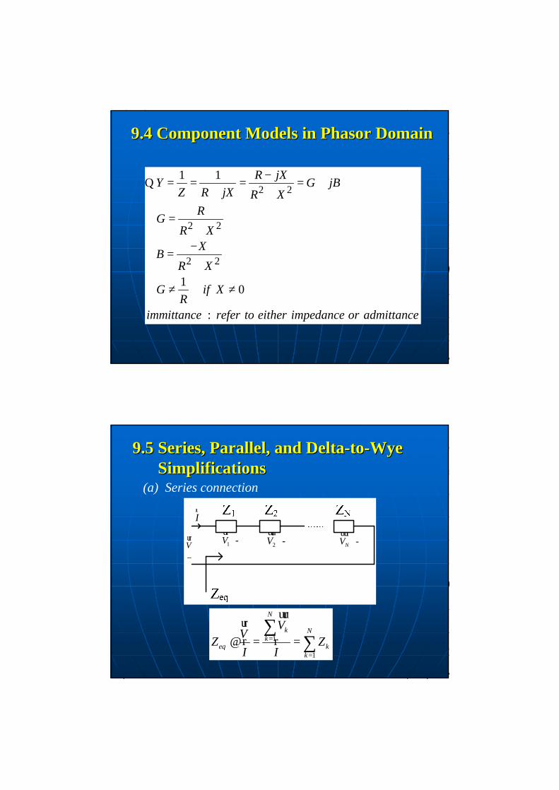
2 2
2 2
2 2
1 1
1 0
:
R jXY G jBZ R jX R X
RGR X
XBR X
G if XR
immittance refer to either impedance or admittance
−= = = = +
+ +
∴ =+
−=
+
∴ ≠ ≠
Q
9.4 Component Models in Phasor Domain9.4 Component Models in Phasor Domain
(a) Series connection
Ir
V
+
−
ur1 -V+
ur2 -V+
uur -NV+uur
1
1
N
k Nk
eq kk
VVZ ZI I
=
=
= =∑
∑
uururr r@
9.5 Series, Parallel, and Delta9.5 Series, Parallel, and Delta--toto--Wye Wye SimplificationsSimplifications
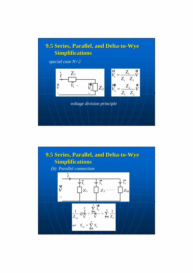
special case N=2
Ir
V
+
−
ur1 -V+
ur
2-V+uur
11
1 2
22
1 2
ZV VZ Z
ZV VZ Z
=+
=+
ur ur
uur ur
voltage division principle
9.5 Series, Parallel, and Delta9.5 Series, Parallel, and Delta--toto--Wye Wye SimplificationsSimplifications
(b) Parallel connection
1Iur
2Iuur
NIuur
V
+
−
ur
Ir
1
1
1
1 1
N
k Nk
keq k
N
eq kk
II
Z ZV V
or Y Y
=
=
=
= =
=
∑∑
∑
uurrur ur@
9.5 Series, Parallel, and Delta9.5 Series, Parallel, and Delta--toto--Wye Wye SimplificationsSimplifications
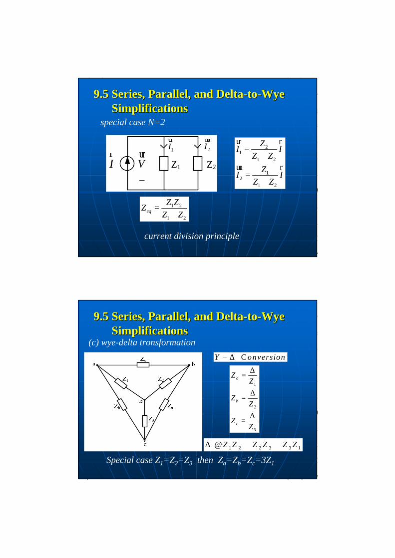
special case N=2
Z1 Z2
1Iur
2Iuur
V
+
−
urIr
21
1 2
12
1 2
ZI IZ Z
ZI IZ Z
=+
=+
ur r
uur r
1 2
1 2eq
Z ZZZ Z
=+
current division principle
9.5 Series, Parallel, and Delta9.5 Series, Parallel, and Delta--toto--Wye Wye SimplificationsSimplifications
(c) wye-delta tronsformation CY onversion− ∆
1
2
3
a
b
c
ZZ
ZZ
ZZ
∆=
∆=
∆=
1 2 2 3 3 1Z Z Z Z Z Z∆ + +@
Special case Z1=Z2=Z3 then Za=Zb=Zc=3Z1
9.5 Series, Parallel, and Delta9.5 Series, Parallel, and Delta--toto--Wye Wye SimplificationsSimplifications
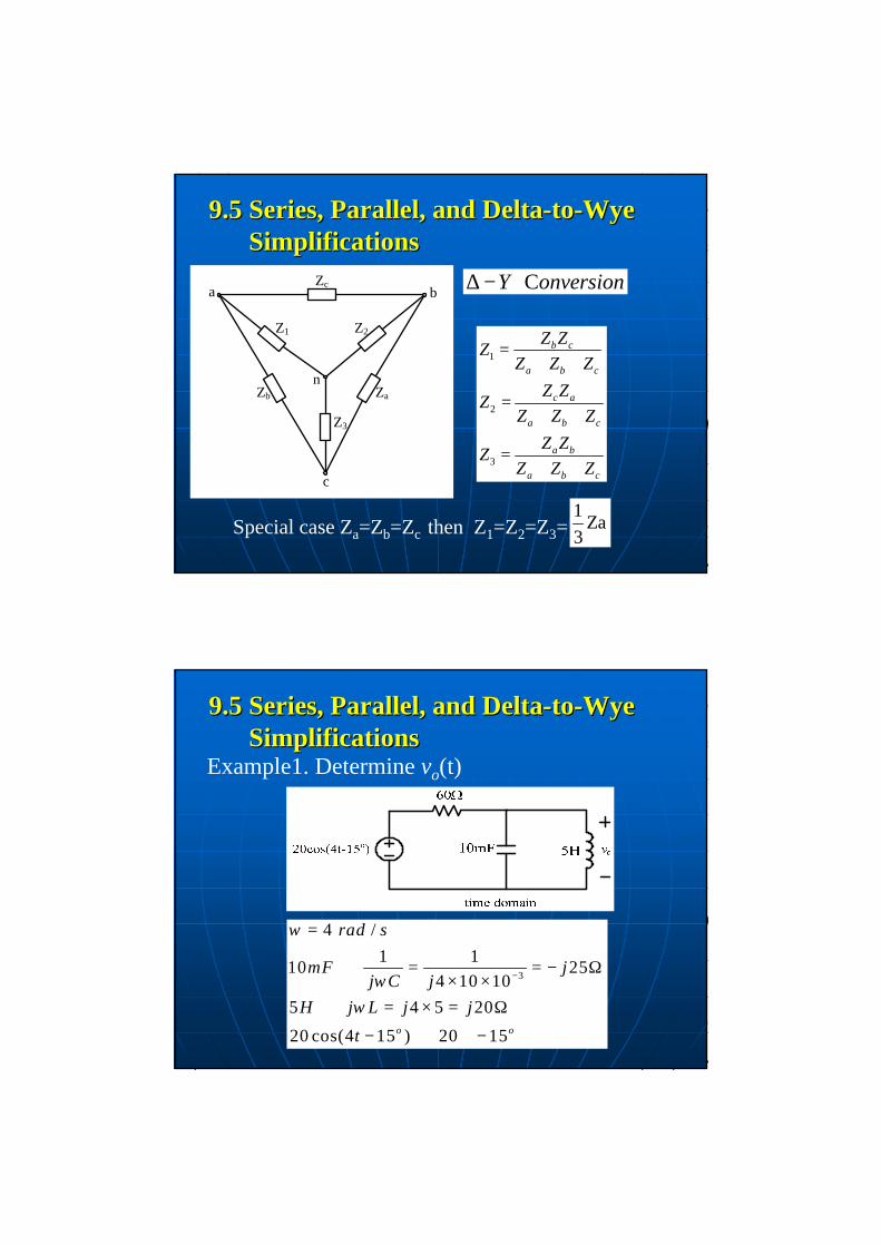
1
2
3
b c
a b c
c a
a b c
a b
a b c
Z ZZZ Z Z
Z ZZZ Z Z
Z ZZZ Z Z
=+ +
=+ +
=+ +
Special case Za=Zb=Zc then Z1=Z2=Z3=1 Za3
CY onversion∆ −a b
c
Z1 Z2
Z3
Zc
Zb Zan
9.5 Series, Parallel, and Delta9.5 Series, Parallel, and Delta--toto--Wye Wye SimplificationsSimplifications
Example1. Determine vo(t)
3
4 /1 110 25
4 10 105 4 5 2020 cos(4 15 ) 20 15o o
rad s
mF jj C j
H j L j jt
ω
ωω
−
=
⇒ = = − Ω× ×
⇒ = × = Ω
− ⇒ ∠ −
9.5 Series, Parallel, and Delta9.5 Series, Parallel, and Delta--toto--Wye Wye SimplificationsSimplifications
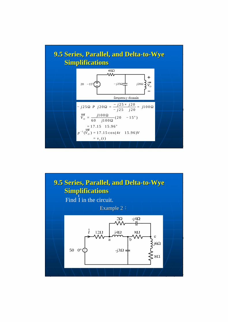
20 15o∠ − 25j− Ω 20j ΩOV
uur
1
2 5 2 02 5 2 0 1 0 02 5 2 0
1 0 0 ( 2 0 1 5 )6 0 1 0 0
1 7 .1 5 1 5 .9 6
( ) 1 7 .1 5 c o s ( 4 1 5 .9 6 ) ( )
oO
o
O
o
j jj j jj j
jVj
p V t Vv t
−
− ×− Ω Ω = = Ω
− +Ω
∴ = ∠ −+ Ω
= ∠
= +
=
uur
uur
P
9.5 Series, Parallel, and Delta9.5 Series, Parallel, and Delta--toto--Wye Wye SimplificationsSimplifications
Example 2Example 2::
Ir
50 0∠ °
Find I in the circuit.r
9.5 Series, Parallel, and Delta9.5 Series, Parallel, and Delta--toto--Wye Wye SimplificationsSimplifications
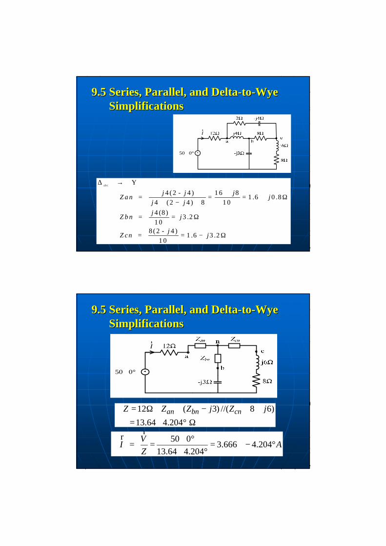
ab c Y4 ( 2 - 4 ) 1 6 8 1 .6 0 .8
4 ( 2 4 ) 8 1 04 (8 ) 3 .21 0
8( 2 - 4 ) 1 .6 3 .21 0
j j jZ a n jj jjZ b n j
jZ cn j
∆ →+
= = = + Ω+ − +
= = Ω
= = − Ω
Ir
50 0∠ °
9.5 Series, Parallel, and Delta9.5 Series, Parallel, and Delta--toto--Wye Wye SimplificationsSimplifications
50 0∠ °
Ir
12 ( 3) //( 8 6) 13.64 4.204
an bn cnZ Z Z j Z j∴ = Ω + + − + +
= ∠ ° Ω
50 0 3.666 4.20413.64 4.204
VI AZ
∠ °∴ = = = ∠ − °
∠ °
rr
9.5 Series, Parallel, and Delta9.5 Series, Parallel, and Delta--toto--Wye Wye SimplificationsSimplifications
4141C.T. PanC.T. Pan 4141
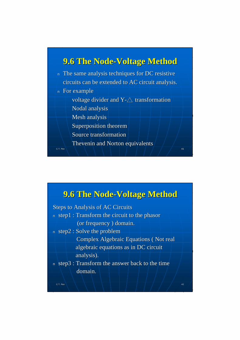
9.6 The Node9.6 The Node--Voltage MethodVoltage Methodnn The same analysis techniques for DC resistive The same analysis techniques for DC resistive
circuits can be extended to AC circuit analysis.circuits can be extended to AC circuit analysis.nn For example For example
voltage divider and Yvoltage divider and Y-- transformation transformation Nodal analysis Nodal analysis Mesh analysis Mesh analysis Superposition theoremSuperposition theoremSource transformationSource transformationThevenin and Norton equivalentsThevenin and Norton equivalents
Steps to Analysis of AC CircuitsSteps to Analysis of AC Circuitsnn step1 : Transform the circuit to the phasor step1 : Transform the circuit to the phasor
(or frequency ) domain.(or frequency ) domain.nn step2 : Solve the problem step2 : Solve the problem
Complex Algebraic Equations ( Not realComplex Algebraic Equations ( Not realalgebraic equations as in DC circuit algebraic equations as in DC circuit analysis).analysis).
nn step3 : Transform the answer back to the time step3 : Transform the answer back to the time domain. domain.
C.T. PanC.T. Pan 4242
9.6 The Node9.6 The Node--Voltage MethodVoltage Method
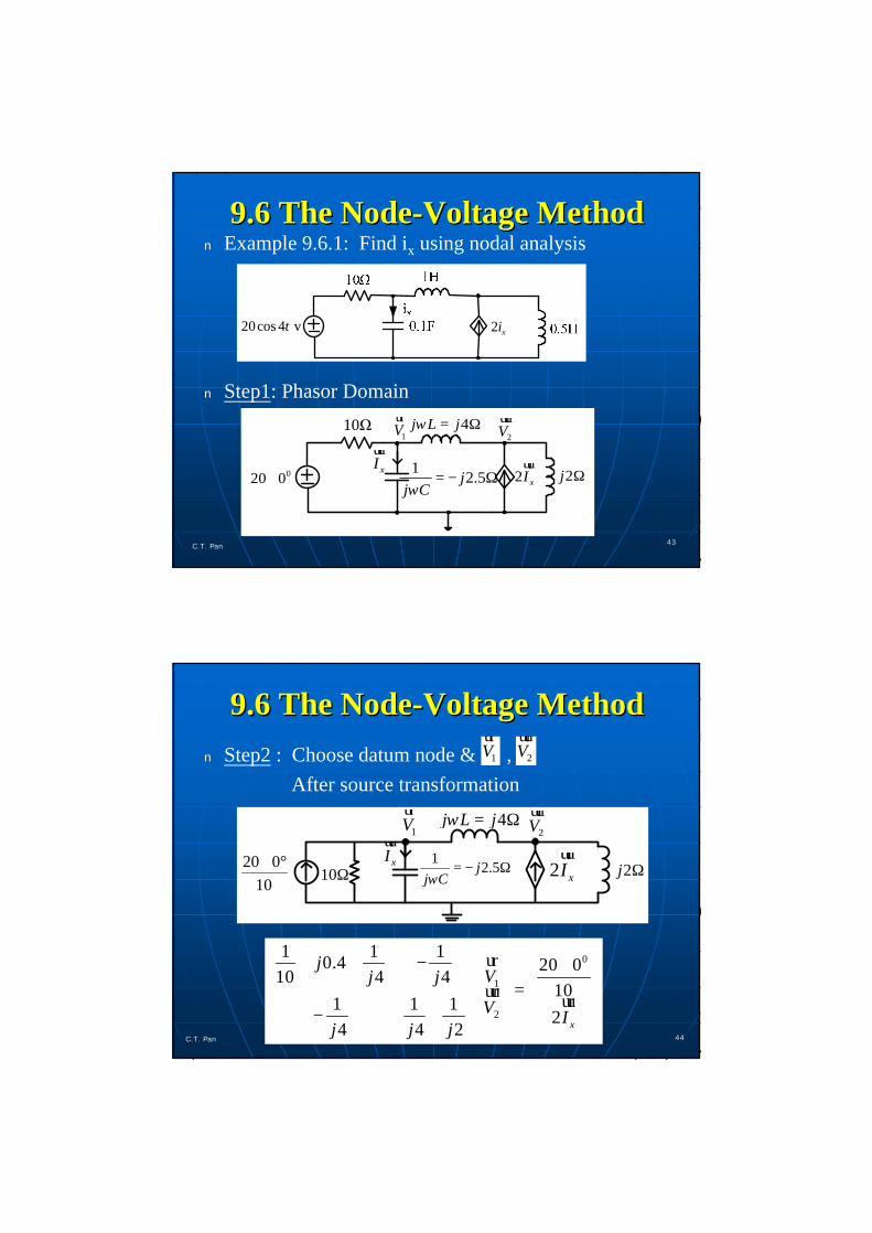
n Example 9.6.1: Find ix using nodal analysis
n Step1: Phasor Domain
20cos 4 vt 2 xi
10Ω
020 0∠
4j L jω = Ω1V
ur2V
uur
1 2.5jj Cω
= − Ω 2 xIuur
2j ΩxIuur
C.T. PanC.T. Pan 4343
9.6 The Node9.6 The Node--Voltage MethodVoltage Method
C.T. PanC.T. Pan 4444
n Step2 : Choose datum node & , After source transformation
0
1
2
1 1 10.4 20 010 4 4
101 1 1
24 4 2 x
jVj j
V Ij j j
+ + − ∠ = − +
ur
uur uur
9.6 The Node9.6 The Node--Voltage MethodVoltage Method1V
ur2V
uur
xIuur
20 010∠ °
10Ω1 2.5j
j Cω= − Ω
4j L jω = Ω1V
ur2V
uur
2 xIuur
2j Ω
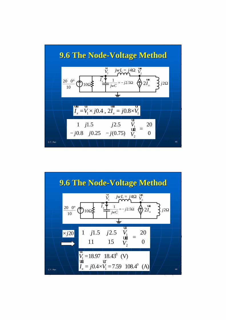
9.6 The Node9.6 The Node--Voltage MethodVoltage Method
C.T. PanC.T. Pan 4545
1 10.4 , 2 0.8x xI V j I j V= × = ×uur ur uur ur
1
2
1 1.5 2.5 200.8 0.25 (0.75) 0
Vj jj j j V
+ = − + −
ur
uur
xIuur
20 010∠ °
10Ω1 2.5j
j Cω= − Ω
4j L jω = Ω1V
ur2V
uur
2 xIuur
2j Ω
C.T. PanC.T. Pan 4646
1
2
1 1.5 2.5 2011 15 0
Vj j
V
+ =
ur
uur
01
01
18.97 18.43 (V)
0.4 7.59 108.4 (A)x
V
I j V
= ∠
= × = ∠
ur
uur ur
20j×
9.6 The Node9.6 The Node--Voltage MethodVoltage Method
xIuur
20 010∠ °
10Ω1 2.5j
j Cω= − Ω
4j L jω = Ω1V
ur2V
uur
2 xIuur
2j Ω
9.6 The Node9.6 The Node--Voltage MethodVoltage Method
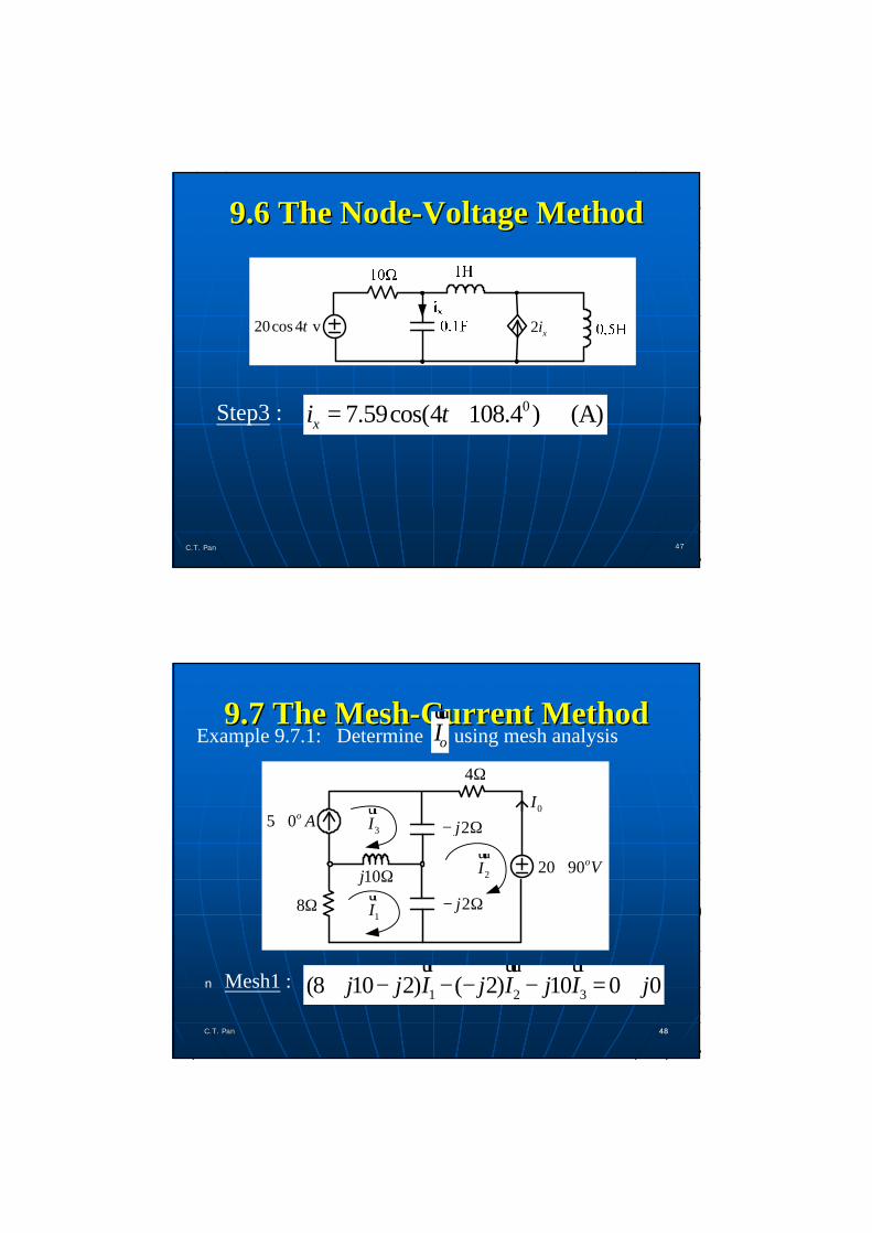
C.T. PanC.T. Pan 4747
Step3 : 07.59cos(4 108.4 ) (A)xi t= +
20cos 4 vt 2 xi
4848C.T. PanC.T. Pan 4848
9.7 The Mesh9.7 The Mesh--Current Method Current Method Example 9.7.1: Determine using mesh analysisoI
uur
20 90oV∠
0I5 0o A∠ 2j− Ω
2j− Ω
10j Ω
8Ω
3Iur
1Iur
2Iuur
4Ω
1 2 3(8 10 2) ( 2) 10 0 0j j I j I j I j+ − − − − = +ur uur ur
n Mesh1 :
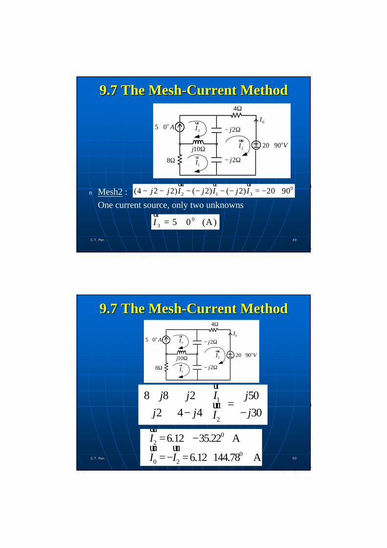
9.7 The Mesh9.7 The Mesh--Current Method Current Method
C.T. PanC.T. Pan 4949
n Mesh2 :One current source, only two unknowns
02 1 3(4 2 2) ( 2) ( 2) 20 90j j I j I j I− − − − − − = − ∠
uur ur ur
20 90oV∠
0I5 0o A∠ 2j− Ω
2j− Ω
10j Ω
8Ω
3Iur
1Iur
2Iuur
4Ω
03 5 0 (A )I = ∠
ur
9.7 The Mesh9.7 The Mesh--Current Method Current Method
C.T. PanC.T. Pan 5050
20 90oV∠
0I5 0o A∠ 2j− Ω
2j− Ω
10j Ω
8Ω
3Iur
1Iur
2Iuur
4Ω
1
2
8 8 2 502 4 4 30
Ij j jj j jI
+ = − −
ur
uur
02
00 2
6.12 35.22 A
6.12 144.78 A
I
I I
∴ = ∠−
∴ = − = ∠
uur
uur uur
5151C.T. PanC.T. Pan 5151
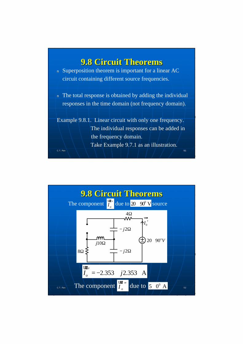
9.8 Circuit Theorems9.8 Circuit Theoremsn Superposition theorem is important for a linear AC
circuit containing different source frequencies.
n The total response is obtained by adding the individual responses in the time domain (not frequency domain).
Example 9.8.1. Linear circuit with only one frequency.The individual responses can be added inthe frequency domain.Take Example 9.7.1 as an illustration.
9.8 Circuit Theorems9.8 Circuit TheoremsThe component due to source
oI ′uur 020 90 V∠
20 90oV∠
0I ′uur
2j− Ω
2j− Ω
10j Ω
8Ω
4Ω
2.353 2.353 AoI j′ = − +uur
C.T. PanC.T. Pan 5252The component due tooI ′′uur 05 0 A∠
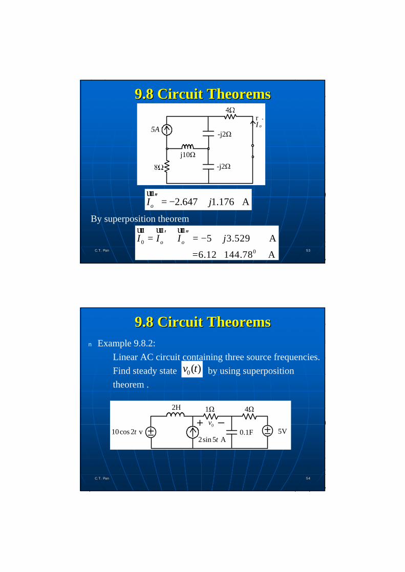
9.8 Circuit Theorems9.8 Circuit Theorems
5A -j2Ω
-j2Ωj10Ω
''oI
r
C.T. PanC.T. Pan 5353
2.647 1.176 AoI j′′ = − +uur
By superposition theorem
00
5 3.529 A
=6.12 144.78 Ao oI I I j′ ′′= + = − +
∠
uur uur uur
9.8 Circuit Theorems9.8 Circuit Theorems
5454C.T. PanC.T. Pan
n Example 9.8.2: Linear AC circuit containing three source frequencies.Find steady state by using superposition theorem .
0( )v t
4Ω1Ω
0.1F
2H
10cos 2 vt0v
2sin 5 At5V
9.8 Circuit Theorems9.8 Circuit Theorems
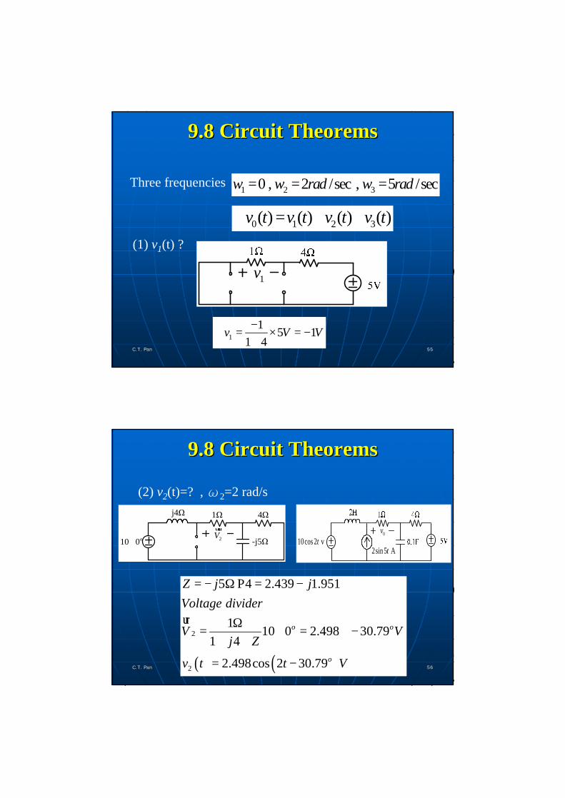
5555C.T. PanC.T. Pan
Three frequencies1 2 30 , 2 /sec , 5 /secrad radω ω ω= = =
0 1 2 3( ) ( ) ( ) ( )v t v t v t v t∴ = + +
1v
11 5 1
1 4v V V−
∴ = × = −+
(1) v1(t) ?
9.8 Circuit Theorems9.8 Circuit Theorems
(2) v2(t)=? , ω2=2 rad/s4Ω1Ω
-j5Ω
j4Ω
10 0o∠ 2Vuur
C.T. PanC.T. Pan 5656
10cos 2 vt0v
2sin 5 At
( ) ( )
2
2
5 4 2.439 1.951 1 10 0 2.498 30.79
1 4
2.498cos 2 30.79
o o
o
Z j jVoltage divider
V Vj Z
v t t V
= − Ω = −
Ω= ∠ = ∠ −
+ +
= −
P
ur
9.8 Circuit Theorems9.8 Circuit Theorems
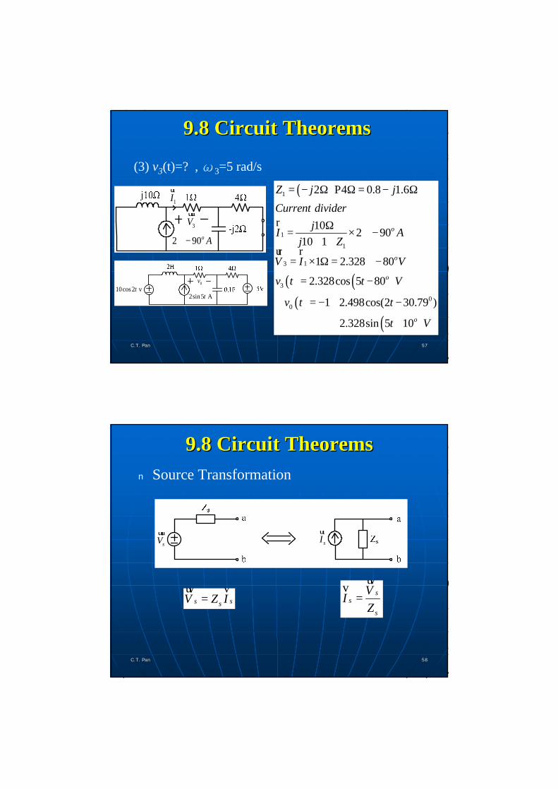
(3) v3(t)=? , ω3=5 rad/s
2 90o A∠ −
3Vuur
1Iur
10cos 2 vt0v
2sin 5 At
( )
( ) ( )( )
( )
1
1
1
13
3
00
2 4 0.8 1.6 10 2 90
10 1
1 2.328 80
2.328cos 5 80
1 2.498cos(2 30.79 )
2.328sin 5 10
o
o
o
o
Z j jCurrent divider
jI Aj Z
V I V
v t t V
v t t
t V
= − Ω Ω = − Ω
Ω= × ∠ −
+ +
= × Ω = ∠ −
= −
∴ = − + −
+ +
P
r
ur r
C.T. PanC.T. Pan 5757
9.8 Circuit Theorems9.8 Circuit Theorems
5858C.T. PanC.T. Pan
n Source Transformation
sVuur
sIur
ss sV Z I=uv v s
s
s
VIZ
=uvv
5959C.T. PanC.T. Pan
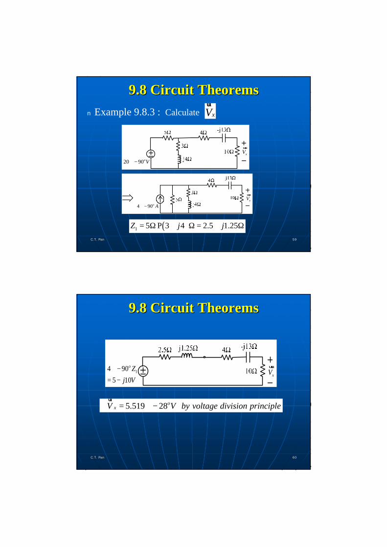
9.8 Circuit Theorems9.8 Circuit Theoremsn Example 9.8.3 : Calculate xV
ur
20 90oV∠ −xV
uur
4 90o A∠ −xV
uur
( )1 5 3 4 2.5 1.25Z j j= Ω + Ω = + ΩP
6060C.T. PanC.T. Pan
9.8 Circuit Theorems9.8 Circuit Theorems
14 905 10
o Zj V
∠ −= −
xVuur
5.519 28 oxV V by voltage division principle∴ = ∠ −
ur

6161C.T. PanC.T. Pan
9.8 Circuit Theorems9.8 Circuit Theoremsnn Thevenin and Norton Equivalent CircuitsThevenin and Norton Equivalent Circuits
A linear two terminal circuit under sinusoidal steady state condition
THVur
NIr
THV =V No N
TH N
I ZZ Z
=
=
ur ur r/N s TH TH
N TH
I I V ZZ Z
= ==
r r ur
9.8 Circuit Theorems9.8 Circuit Theorems
C.T. PanC.T. Pan 6262
Example 9.8.4 : Find the Thevenin equivalent
0120 75 V∠
120 75oV∠
( ) ( )6 8 4 12 6.48 2.64
THZ j jj
= − Ω Ω + Ω Ω
= − Ω
P P
9.8 Circuit Theorems9.8 Circuit Theorems
C.T. PanC.T. Pan 6363
8 12 120 75 8 6 4 12
37.95 220.31
oTH ab a b
o
voltage division
jV V V V Vj j
V
∴ = = − = − ∠ − +
= ∠
ur ur ur ur
THVur
ZTHa
b
9.8 Circuit Theorems9.8 Circuit Theoremsn Example 9.8.5 : Obtain using Norton’s theoremoI
r
40 90oV∠
oIr
3 0o A∠
5 N THZ Z with dead independent sources= = Ω
By superposition theorem40 90 3 0 8 3
5
oo
N s v IVI I I I j A∠
= = + = + ∠ = +Ω
r r r r
C.T. PanC.T. Pan 6464
6565C.T. PanC.T. Pan
9.8 Circuit Theorems9.8 Circuit Theorems
3 0o A∠II
r
NIr
oIr
( )5 1.465 38.48
5 20 15o
o NI I Aj
= = ∠+ +
r r
C.T. PanC.T. Pan 6666
1 11
2 2 2
( ) ( )( ) ( )
v t L M i tdv t M L i tdt
=
Under sinusoidal steady state , given
i1(t)= I1mcos(ωt+θ1)i2(t)= I2mcos(ωt+θ2)
9.9 The Coupling Inductors and 9.9 The Coupling Inductors and Ideal TransformerIdeal Transformer
C.T. PanC.T. Pan 6767
1 1 1
2 2 2
( ) ( )( ) ( )
v t L M i tdv t M L i tdt
=
then v1 =-ωL1I1msin(ωt+θ1)-ωM I2msin(ωt+θ2)
=ωL1I1mcos(ωt+θ1+90°)+ ωM I2mcos(ωt+θ2+90°)v2 =-ωM I1msin(ωt+θ1)-ωL2I2msin(ωt+θ2)
=ωM I1mcos(ωt+θ1+90°)+ ωL2I2mcos(ωt+θ2+90°)
9.9 The Coupling Inductors and 9.9 The Coupling Inductors and Ideal TransformerIdeal Transformer
C.T. PanC.T. Pan 6868
Take phasor transform on both sides
1 1 1 2
2 1 2 2
V j L I j M I
V j M I j L I
ω ω
ω ω
= +
= +
uur ur uur
uur ur uur
9.9 The Coupling Inductors and 9.9 The Coupling Inductors and Ideal TransformerIdeal Transformer
6969C.T. PanC.T. Pan 6969
9.9 The Coupling Inductors and 9.9 The Coupling Inductors and Ideal TransformerIdeal Transformer
1j Lω 2j Lω
j Mω
1Iur
2Iuur
Example 9.9.1: Example 9.9.1: Find the input impedance ZFind the input impedance Zabab of the following circuitof the following circuit
7070C.T. PanC.T. Pan 7070
ZS R1
VS 1j Lω 2j Lω ZL
R2a
b
c
d
j Mω
1Iur
2Iuur
Use mesh current method:Use mesh current method:1 1 1 2
1 2 2 2
( ) (A)
0 ( ) (B)S S
L
V Z R j L I j M I
j M I R j L Z I
ω ω
ω ω
= + + −
= − + + +
uur ur uur
ur uur
From (B)From (B) 2 12 2 L
j MI IR j L Z
ωω
=+ +
uur ur
From (A)From (A)2 2
11 1 1
2 2
( )S SL
M IV Z R j L IR j L Z
ωω
ω= + + +
+ +
uruur ur
9.9 The Coupling Inductors and 9.9 The Coupling Inductors and Ideal TransformerIdeal Transformer
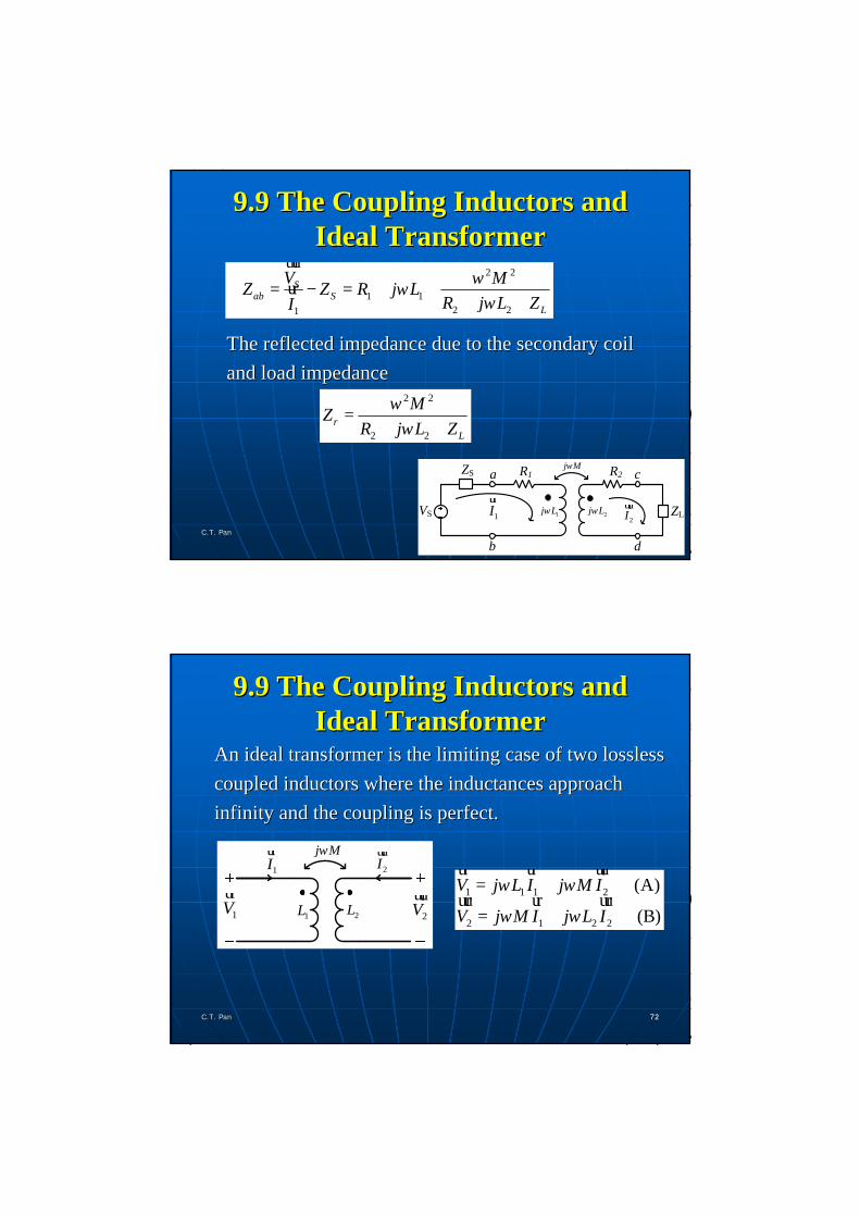
7171C.T. PanC.T. Pan 7171
ZS R1
VS 1j Lω 2j Lω ZL
R2a
b
c
d
j Mω
1Iur
2Iuur
2 2
1 12 21
Sab S
L
V MZ Z R j LR j L ZI
ωω
ω∴ = − = + +
+ +
uurur
The reflected impedance due to the secondary coil The reflected impedance due to the secondary coil and load impedanceand load impedance
2 2
2 2r
L
MZR j L Z
ωω
=+ +
9.9 The Coupling Inductors and 9.9 The Coupling Inductors and Ideal TransformerIdeal Transformer
7272C.T. PanC.T. Pan 7272
An ideal transformer is the limiting case of two lossless An ideal transformer is the limiting case of two lossless coupled inductors where the inductances approach coupled inductors where the inductances approach infinity and the coupling is perfect.infinity and the coupling is perfect.
1Vur
2Vuur
1Iur
2Iuurj Mω
1L 2L1 1 1 2
2 1 2 2
(A)
(B)
V j L I j M I
V j M I j L I
ω ω
ω ω
= +
= +
ur ur uur
uur ur uur
9.9 The Coupling Inductors and 9.9 The Coupling Inductors and Ideal TransformerIdeal Transformer

7373C.T. PanC.T. Pan 7373
1 21
1
(C)V j M IIj L
ωω
−=
ur uururFrom (A)From (A)
Substitute (C) into (B)Substitute (C) into (B)2
2 2 2 1 21 1
M j MV j L I V IL L
ωω= + −
uur uur ur uur
1 21 2
1 Mk M L LL L
= = ⇒ =Q
22 2 2 1 2 2
1
2 21 1
1 1
LV j L I V j L IL
L NV VL N
ω ω∴ = + −
= =
uur uur ur uur
ur ur
9.9 The Coupling Inductors and 9.9 The Coupling Inductors and Ideal TransformerIdeal Transformer
7474C.T. PanC.T. Pan 7474
As LAs L11, L, L22, M , M →∞→∞ such that remains the such that remains the same, the coupled coils become an ideal same, the coupled coils become an ideal transformer.transformer.
2
1
NN
9.9 The Coupling Inductors and 9.9 The Coupling Inductors and Ideal TransformerIdeal Transformer
7575C.T. PanC.T. Pan 7575
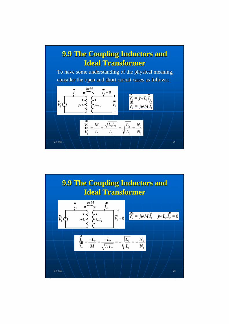
To have some understanding of the physical meaning, To have some understanding of the physical meaning, consider the open and short circuit cases as follows:consider the open and short circuit cases as follows:
1 1 1
2 1
V j L I
V j M I
ω
ω
=
=
ur ur
uur ur
1 22 2 2
1 1 1 11
L LV L NML L L NV
∴ = = = =uurur
1Vur
2Vuur
1Iur
2 0I =uurj Mω
1j Lω 2j Lω
9.9 The Coupling Inductors and 9.9 The Coupling Inductors and Ideal TransformerIdeal Transformer
7676C.T. PanC.T. Pan 7676
2 1 2 2 0V j M I j L Iω ω= + =uur ur uur
1 2 2 2 2
1 12 1 2
I L L L NM L NI L L
− −∴ = = = − = −
uruur
1Vur
2 0V =uur
1Iur
2Iuurj Mω
1j Lω 2j Lω
9.9 The Coupling Inductors and 9.9 The Coupling Inductors and Ideal TransformerIdeal Transformer
7777C.T. PanC.T. Pan 7777
2 2
11
1 2
12
V NNV
I NNI
=
= −
uurur
uruur
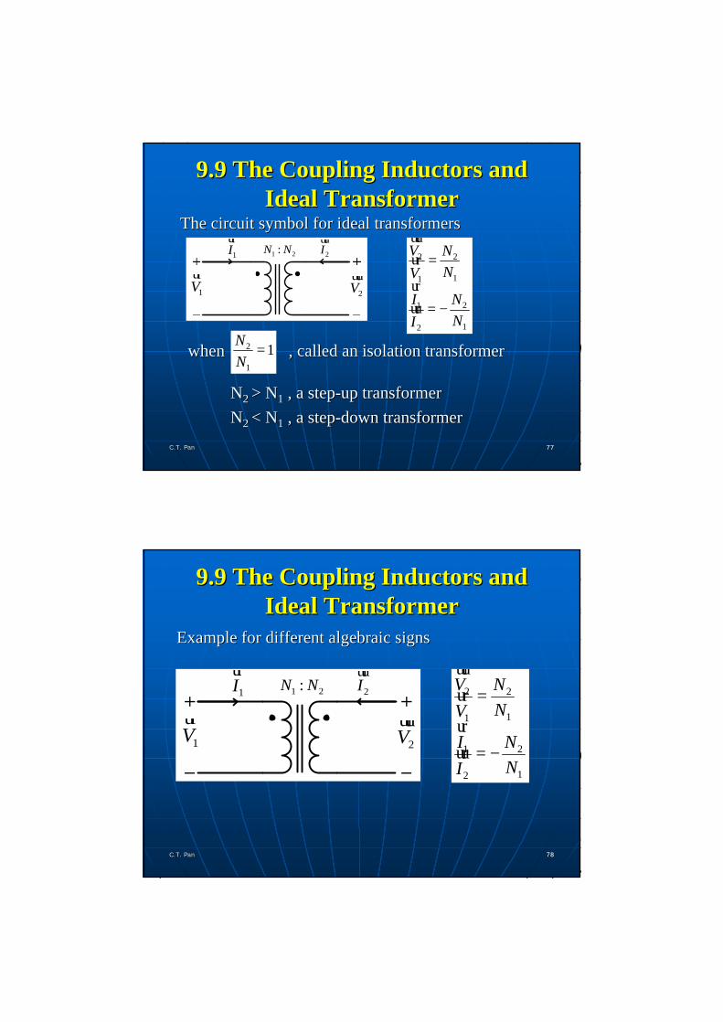
The circuit symbol for ideal transformersThe circuit symbol for ideal transformers
1Vur
2Vuur
1Iur
2Iuur
1 2:N N
when , called an isolation transformerwhen , called an isolation transformer
NN2 2 > N> N11 , a step, a step--up transformerup transformerNN2 2 < N< N11 , a step, a step--down transformerdown transformer
2
1
1NN
=
9.9 The Coupling Inductors and 9.9 The Coupling Inductors and Ideal TransformerIdeal Transformer
7878C.T. PanC.T. Pan 7878
2 2
11
1 2
12
V NNV
I NNI
=
= −
uurur
uruur
Example for different algebraic signsExample for different algebraic signs
1Vur
2Vuur
1Iur
2Iuur
1 2:N N
9.9 The Coupling Inductors and 9.9 The Coupling Inductors and Ideal TransformerIdeal Transformer
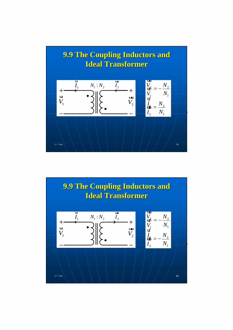
7979C.T. PanC.T. Pan 7979
2 2
11
1 2
12
V NNV
I NNI
= −
=
uurur
uruur1V
ur2V
uur1I
ur2I
uur1 2:N N
9.9 The Coupling Inductors and 9.9 The Coupling Inductors and Ideal TransformerIdeal Transformer
8080C.T. PanC.T. Pan 8080
2 2
11
1 2
12
V NNV
I NNI
= −
= −
uurur
uruur1V
ur2V
uur1I
ur2I
uur1 2:N N
9.9 The Coupling Inductors and 9.9 The Coupling Inductors and Ideal TransformerIdeal Transformer
8181C.T. PanC.T. Pan 8181
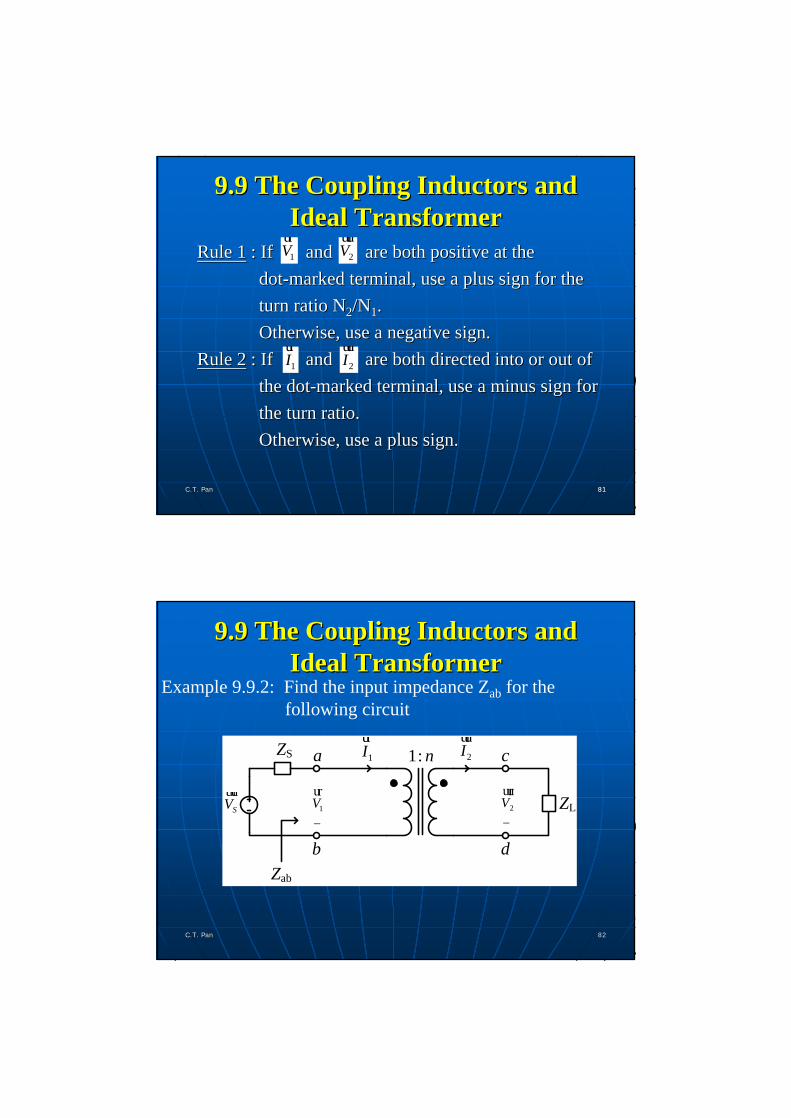
Rule 1Rule 1 : If and are both positive at the : If and are both positive at the dotdot--marked terminal, use a plus sign for the marked terminal, use a plus sign for the turn ratio Nturn ratio N22/N/N11..Otherwise, use a negative sign.Otherwise, use a negative sign.
Rule 2Rule 2 : If and are both directed into or out of : If and are both directed into or out of the dotthe dot--marked terminal, use a minus sign for marked terminal, use a minus sign for the turn ratio.the turn ratio.Otherwise, use a plus sign.Otherwise, use a plus sign.
1Vur
2Vuur
1Iur
2Iuur
9.9 The Coupling Inductors and 9.9 The Coupling Inductors and Ideal TransformerIdeal Transformer
C.T. PanC.T. Pan 8282
Example 9.9.2: Find the input impedance Zab for the following circuit
9.9 The Coupling Inductors and 9.9 The Coupling Inductors and Ideal TransformerIdeal Transformer
ZS
ZL
a
b
c
d
1: n
1V
+
−
ur
2Iuur
1Iur
2V
+
−
uur
Zab
SVuur
C.T. PanC.T. Pan 8383
From the ideal transformer model
2 1
1 2
21 2
ab 2 21 2 2
1 1Z = L
V In nV I
VV Vn Zn nI nI I
= =
∴ = = =
uur uruur uur
uuruur uurur uur uur
,
9.9 The Coupling Inductors and 9.9 The Coupling Inductors and Ideal TransformerIdeal Transformer
ZS
ZL
a
b
c
d
1: n
1V
+
−
ur
2Iuur
1Iur
2V
+
−
uur
Zab
SVuur
C.T. PanC.T. Pan 8484
Hence, ideal transformers can be used to raise or lower the impedance level of a load by choosing proper turn ratio n.
9.9 The Coupling Inductors and 9.9 The Coupling Inductors and Ideal TransformerIdeal Transformer
1: n
1V
+
−
ur
2Iuur
1Iur
2V
+
−
uurSV
uur
C.T. PanC.T. Pan 8585
9.9 The Coupling Inductors and 9.9 The Coupling Inductors and Ideal TransformerIdeal Transformer
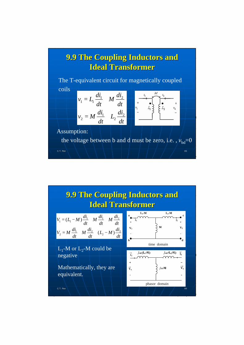
The T-equivalent circuit for magnetically coupled coils
1 21 1
1 22 2
di div L Mdt dtdi div M Ldt dt
= +
= +
Assumption: the voltage between b and d must be zero, i.e. , vbd=0
C.T. PanC.T. Pan 8686
9.9 The Coupling Inductors and 9.9 The Coupling Inductors and Ideal TransformerIdeal Transformer
1 1 21 1
1 2 22 2
( )
( )
di di diV L M M Mdt dt dt
di di diV M M L Mdt dt dt
= − + +
= + + −
L1-M L2-M
M
a
b
c
d
i1 i2
V1 V2
+
-
+
-
time domain
phasor domain
Mathematically, they are equivalent.
L1-M or L2-M could be negative

C.T. PanC.T. Pan 8787
9.9 The Coupling Inductors and 9.9 The Coupling Inductors and Ideal TransformerIdeal Transformer
Modeling of a practical transformer
Ll1,Ll2 : leakage inductancesLm : magnetizing inductanceRc : represents core lossR1,R2 : winding resistancesn : turn ratio of ideal transformer
n Objective 1 : Be able to perform a phasor transform and an inverse phasor transform.
n Objective 2 : Be able to transform a time-domain circuit with a sinusoidal source into frequency domain using phasor concepts.
n Objective 3 : Be able to solve a linear AC circuit under sinusoidal steady state by extending the analysis techniques for DC resistive circuits.
C.T. PanC.T. Pan 8888
SummarySummary
n Objective 4 : Be able to analyze AC circuits containing coupling inductors using phasor methods.
n Objective 5 : Be able to analyze AC circuits containing ideal transformers using phasor methods.
C.T. PanC.T. Pan 8989
SummarySummary
C.T. PanC.T. Pan 9090
SummarySummaryChapter Problems : 9.11(c)
9.199.239.279.379.489.539.619.749.79
Due within one week.

![Circuit Network Analysis - [Chapter2] Sinusoidal Steady-state Analysis](https://static.fdocuments.net/doc/165x107/55d03589bb61ebd3698b46c3/circuit-network-analysis-chapter2-sinusoidal-steady-state-analysis.jpg)