Signals and Systems Lecture 3: Sinusoids. 2 Today's lecture −Sinusoidal signals −Review of the Sine…
Sinusoidal Signals
( ) ( )+= tVtv cosm
f2=
fT
1=
Useful
relations
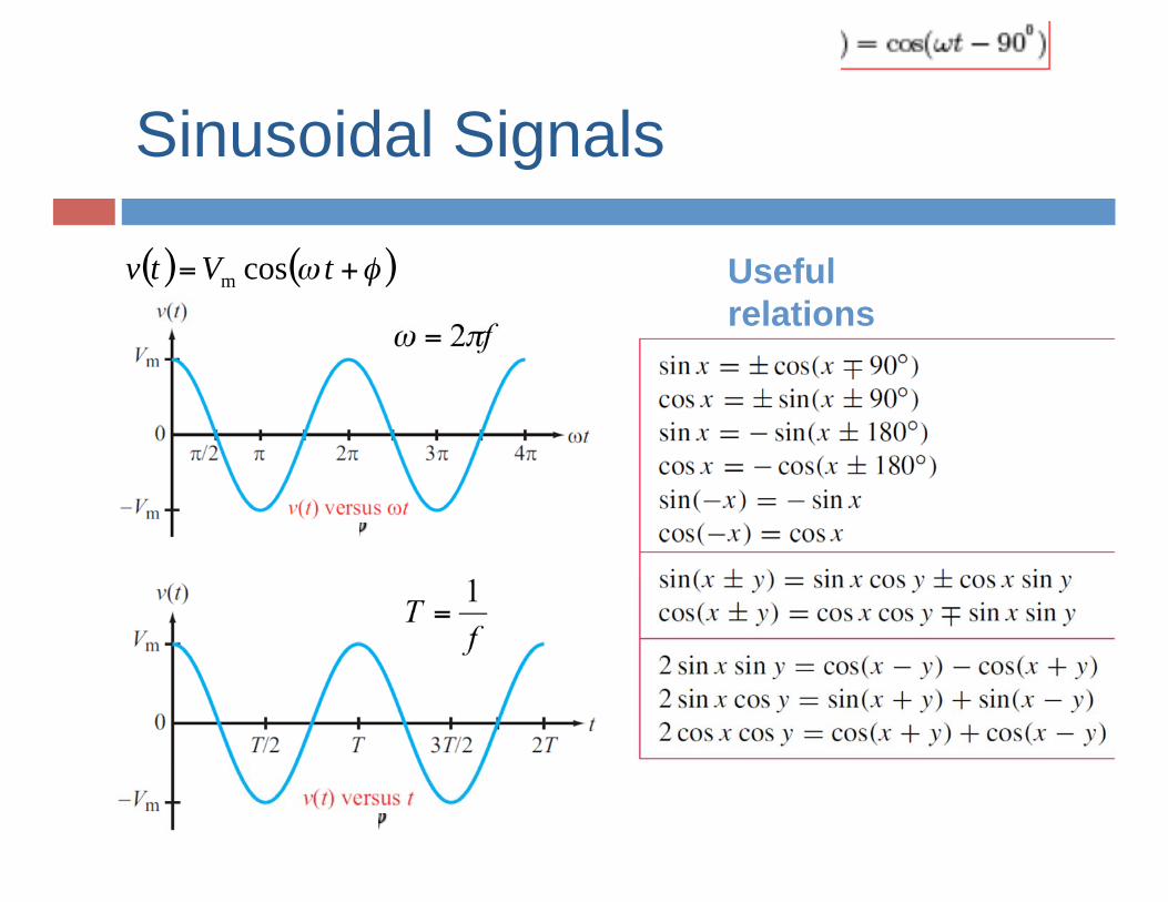
Phase Lead/Lag
Principles of Electrical Engineering I
Motivation to steady state analysis
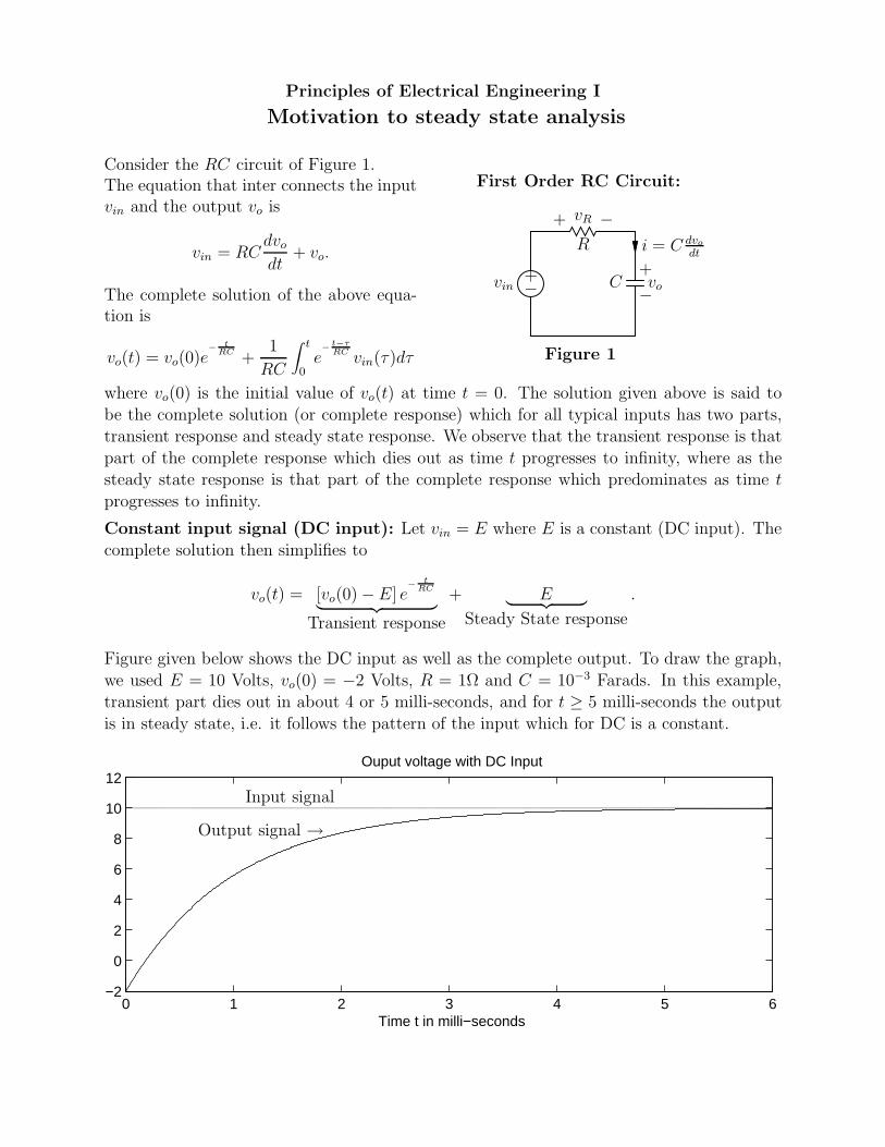
Consider the RC circuit of Figure 1.The equation that inter connects the inputvin and the output vo is
vin = RCdvo
dt+ vo.
The complete solution of the above equa-tion is
vo(t) = vo(0)e−
t
RC +1
RC
∫t
0
e−
t−τ
RC
vin(τ)dτ
First Order RC Circuit:
−+
vin
R
+ vR −
C+vo−
i = Cdvo
dt
Figure 1
where vo(0) is the initial value of vo(t) at time t = 0. The solution given above is said to
be the complete solution (or complete response) which for all typical inputs has two parts,transient response and steady state response. We observe that the transient response is that
part of the complete response which dies out as time t progresses to infinity, where as thesteady state response is that part of the complete response which predominates as time t
progresses to infinity.
Constant input signal (DC input): Let vin = E where E is a constant (DC input). Thecomplete solution then simplifies to
vo(t) = [vo(0) − E] e−
t
RC
︸ ︷︷ ︸
Transient response
+ E︸ ︷︷ ︸
Steady State response
.
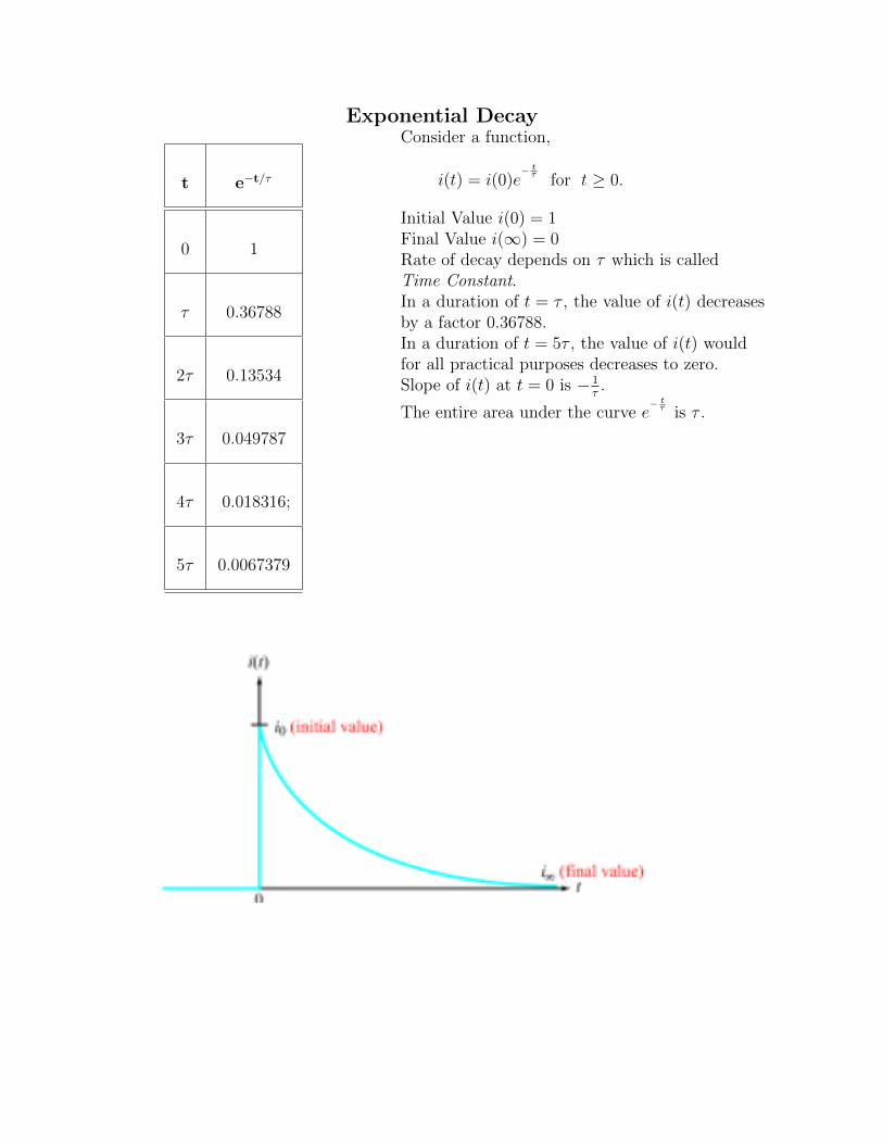
Figure given below shows the DC input as well as the complete output. To draw the graph,
we used E = 10 Volts, vo(0) = −2 Volts, R = 1Ω and C = 10−3 Farads. In this example,transient part dies out in about 4 or 5 milli-seconds, and for t ≥ 5 milli-seconds the output
is in steady state, i.e. it follows the pattern of the input which for DC is a constant.
0 1 2 3 4 5 6−2
0
2
4
6
8
10
12 Ouput voltage with DC Input
Time t in milli−seconds
Input signal
Output signal →
2
Exponential Decay
t e−t/τ
0 1
τ 0.36788
2τ 0.13534
3τ 0.049787
4τ 0.018316;
5τ 0.0067379
Consider a function,
i(t) = i(0)e− tτ for t ≥ 0.
Initial Value i(0) = 1Final Value i(∞) = 0Rate of decay depends on τ which is calledTime Constant.In a duration of t = τ , the value of i(t) decreasesby a factor 0.36788.In a duration of t = 5τ , the value of i(t) wouldfor all practical purposes decreases to zero.Slope of i(t) at t = 0 is − 1
τ.
The entire area under the curve e− tτ is τ .
2
Alternating input signal (AC input): Let vin = A cos(ωt) where ω is the angularfrequency in radians per second and A is the amplitude of the sinusoidal voltgae in Volts
(AC input). The complete solution then simplifies to
vo(t) =[
vo(0) −A
1 + ω2R2C2
]
e−
t
RC
︸ ︷︷ ︸
Transient response
+A
1 + ω2R2C2[cos(ωt) + ωRC sin(ωt)]
︸ ︷︷ ︸
Steady State response
=[
vo(0) −A
1 + ω2R2C2
]
e−
t
RC
︸ ︷︷ ︸
Transient response
+A√
1 + ω2R2C2[cos(ωt − θ)]
︸ ︷︷ ︸
Steady State response
where θ = tan−1(ωRC).
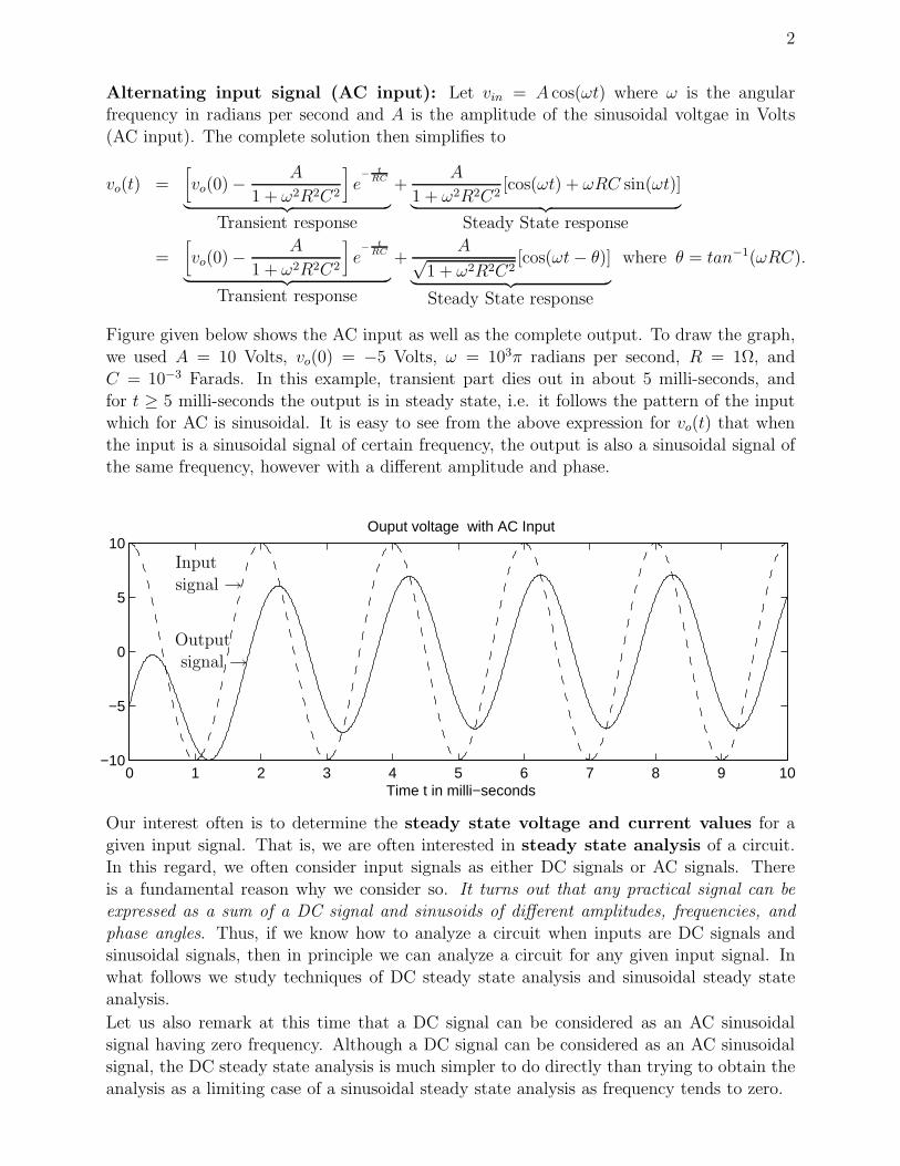
Figure given below shows the AC input as well as the complete output. To draw the graph,
we used A = 10 Volts, vo(0) = −5 Volts, ω = 103π radians per second, R = 1Ω, andC = 10−3 Farads. In this example, transient part dies out in about 5 milli-seconds, and
for t ≥ 5 milli-seconds the output is in steady state, i.e. it follows the pattern of the inputwhich for AC is sinusoidal. It is easy to see from the above expression for vo(t) that when
the input is a sinusoidal signal of certain frequency, the output is also a sinusoidal signal ofthe same frequency, however with a different amplitude and phase.
0 1 2 3 4 5 6 7 8 9 10−10
−5
0
5
10 Ouput voltage with AC Input
Time t in milli−seconds
Input
signal →
Outputsignal →
Our interest often is to determine the steady state voltage and current values for a
given input signal. That is, we are often interested in steady state analysis of a circuit.In this regard, we often consider input signals as either DC signals or AC signals. There
is a fundamental reason why we consider so. It turns out that any practical signal can be
expressed as a sum of a DC signal and sinusoids of different amplitudes, frequencies, and
phase angles. Thus, if we know how to analyze a circuit when inputs are DC signals andsinusoidal signals, then in principle we can analyze a circuit for any given input signal. In
what follows we study techniques of DC steady state analysis and sinusoidal steady stateanalysis.
Let us also remark at this time that a DC signal can be considered as an AC sinusoidal
signal having zero frequency. Although a DC signal can be considered as an AC sinusoidalsignal, the DC steady state analysis is much simpler to do directly than trying to obtain the
analysis as a limiting case of a sinusoidal steady state analysis as frequency tends to zero.
Principles of Electrical Engineering I
Motivation to introduce phasors
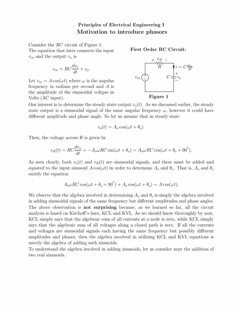
Consider the RC circuit of Figure 1.The equation that inter connects the inputvin and the output vo is
vin = RCdvo
dt+ vo.
Let vin = A cos(ωt) where ω is the angularfrequency in radians per second and A isthe amplitude of the sinusoidal voltgae inVolts (AC input).
First Order RC Circuit:
−+
vin
R
+ vR −
C+vo−
i = Cdvo
dt
Figure 1
Our interest is to determine the steady state output vo(t). As we discussed earlier, the steadystate output is a sinusoidal signal of the same angular frequency ω, however it could have
different amplitude and phase angle. So let us assume that in steady state
vo(t) = Ao cos(ωt + θo).
Then, the voltage across R is given by
vR(t) = RCdvo
dt= −AoωRC sin(ωt + θo) = AoωRC cos(ωt + θo + 90
0
).
As seen clearly, both vo(t) and vR(t) are sinusoidal signals, and these must be added and
equated to the input sinusoid A cos(ωt) in order to determine Ao and θo. That is, Ao and θo
satisfy the equation
AoωRC cos(ωt + θo + 900
) + Ao cos(ωt + θo) = A cos(ωt).
We observe that the algebra involved in determining Ao and θo is simply the algebra involvedin adding sinusoidal signals of the same frequency but different amplitudes and phase angles.
The above observation is not surprising because, as we learned so far, all the circuitanalysis is based on Kirchoff’s laws, KCL and KVL. As we should know thoroughly by now,
KCL simply says that the algebraic sum of all currents at a node is zero, while KCL simplysays that the algebraic sum of all voltages along a closed path is zero. If all the currents
and voltages are sinusoidal signals each having the same frequency but possibly different
amplitudes and phases, then the algebra involved in utilizing KCL and KVL equations ismerely the algebra of adding such sinusoids.
To understand the algebra involved in adding sinusoids, let us consider next the addition oftwo real sinusoids.
2
Example of adding two real sinusoids: Determine the sum of two sinusoidal signalsx1(t) and x2(t). That is, determine x(t) = x1(t) + x2(t), where
x1(t) = A1 cos(ωt + θ1) and x2(t) = A2 cos(ωt + θ2).
By using trigonometry, we can rewrite
A1 cos(ωt + θ1) = A1 cos(θ1) cos(ωt) − A1 sin(θ1) sin(ωt)
A2 cos(ωt + θ2) = A2 cos(θ2) cos(ωt) − A2 sin(θ2) sin(ωt).
Thus, we note that
x(t) = x1(t) + x2(t)
x(t) = A1 cos(ωt + θ1) + A2 cos(ωt + θ2)
= [A1 cos(θ1) + A2 cos(θ2)] cos(ωt) − [A1 sin(θ1) + A2 sin(θ2)] sin(ωt)
= A cos(θ) cos(ωt) − A sin(θ)sin(ωt)
= A cos(ωt + θ),
where
A1 cos(θ1) + A2 cos(θ2) = A cos(θ) and A1 sin(θ1) + A2 sin(θ2) = A sin(θ).
The above equations together can be rewritten in conventional polar coordinate notation ofadding two vectors as
A6 θ = A1 6 θ1 + A2 6 θ2. (∗)The above analysis shows that the sum of two real sinusoids of the same frequency is another
real sinusoid of the same frequency whose amplitude and phase angle is given by the aboveequation. The above equation does not depend at all on time t. It merely depends on the
amplitudes and phase angles of the given real sinusoids.
Important Observation: The sum of two real sinusoids is another real sinusoid whoseamplitude and phase are given by equation (*). A simple study of equation (*) reveals that
it is simply the sum of two vectors yielding a resultant vector. In Electrical Engineering, avector derived from the amplitude and phase of a sinusoid is called a phasor. Thus, the
equation (*) represents indeed a sum of two phasors to yield another phasor.
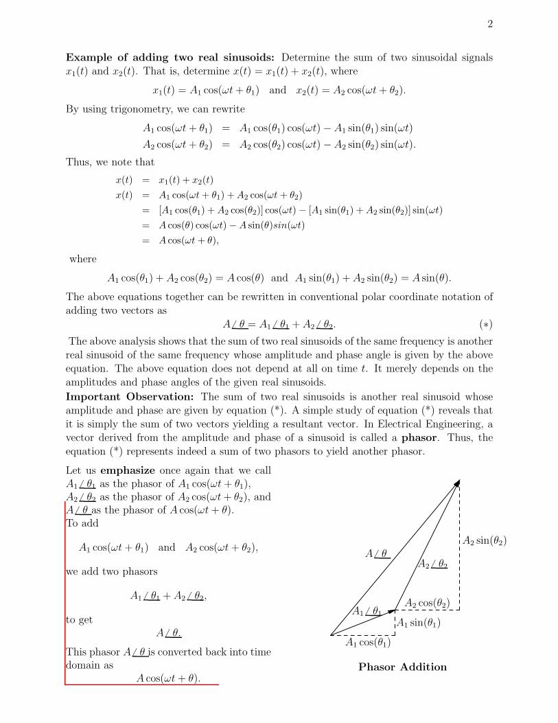
Let us emphasize once again that we callA1 6 θ1 as the phasor of A1 cos(ωt + θ1),A2 6 θ2 as the phasor of A2 cos(ωt + θ2), andA6 θ as the phasor of A cos(ωt + θ).To add
A1 cos(ωt + θ1) and A2 cos(ωt + θ2),
we add two phasors
A1 6 θ1 + A2 6 θ2,
to getA6 θ.
This phasor A6 θ is converted back into timedomain as
A cos(ωt + θ).Phasor Addition
A1 cos(θ1)
A1 sin(θ1)
A2 cos(θ2)
A2 sin(θ2)A6 θ
A2 6 θ2
A1 6 θ1
3
Phasor and Inverse Phasor Transformations
Two real sinusoidsA1 cos(ωt + θ1) and A2 cos(ωt + θ2)
when added results in another real sinusoid
A cos(ωt + θ).
In order to obtain the amplitude A and the phase angle θ of the resulting real sinusoid, we
do the following arithmetic,A1 6 θ1 + A2 6 θ2 = A6 θ.
We callA1 6 θ1 as the phasor of A1 cos(ωt + θ1),
A2 6 θ2 as the phasor of A2 cos(ωt + θ2), andA6 θ as the phasor of A cos(ωt + θ).
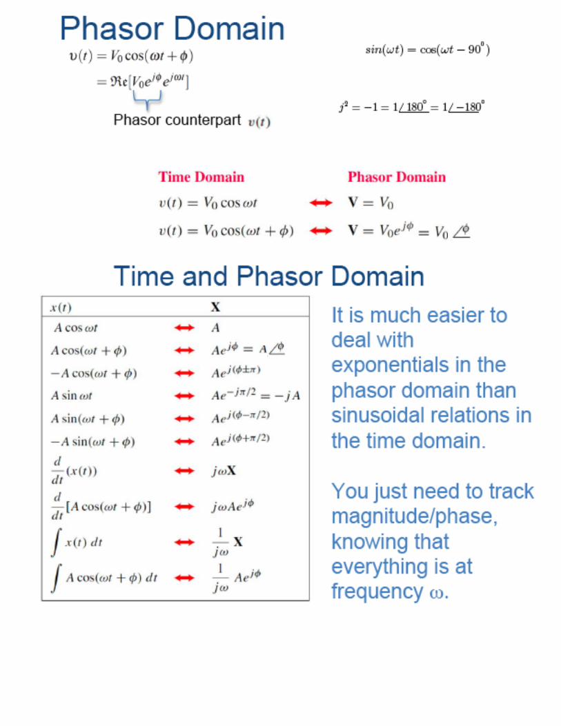
The above discussion leads us to the following Phasor and Inverse Phasor Transformations.
When we use cos(ωt) as the reference sinusoid, we have the following transformation fromtime domain to phasor domain:
T ime domain Phasor domain
A cos(ωt + θ) ⇒ Aejθ = A6 θ.
When we use cos(ωt) as the reference sinusoid, we have the following inverse transformation
from phasor domain to time domain:
Phasor domain T ime domain
Aejθ = A6 θ ⇒ A cos(ωt + θ).
In order to learn more about phasors and phasor domain analysis,we need to review complex numbers.
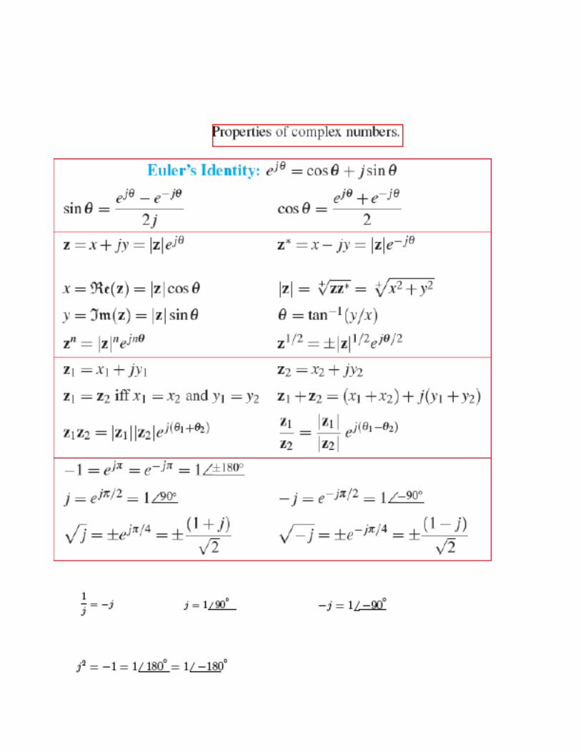
Review of Complex Numbers
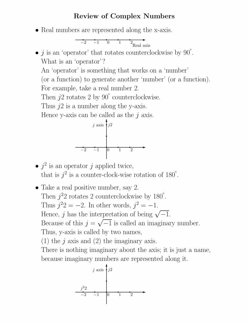
• Real numbers are represented along the x-axis.-•−2 −1 0 1 2
•
Real axis
• • •
• j is an ‘operator’ that rotates counterclockwise by 900
.
What is an ‘operator’?
An ‘operator’ is something that works on a ‘number’
(or a function) to generate another ‘number’ (or a function).
For example, take a real number 2.
Then j2 rotates 2 by 900
counterclockwise.
Thus j2 is a number along the y-axis.
Hence y-axis can be called as the j axis.
-
6j axis
•
• j2
•−2 −1 0 1 2• • • •
• j2 is an operator j applied twice,
that is j2 is a counter-clock-wise rotation of 1800
.
• Take a real positive number, say 2.
Then j22 rotates 2 counterclockwise by 1800
.
Thus j22 = −2. In other words, j2 = −1.
Hence, j has the interpretation of being√
−1.
Because of this j =√
−1 is called an imaginary number.
Thus, y-axis is called by two names,
(1) the j axis and (2) the imaginary axis.
There is nothing imaginary about the axis; it is just a name,
because imaginary numbers are represented along it.
-
6j axis
•
• j2
•−2
j22
−1 0 1 2• • • •
2
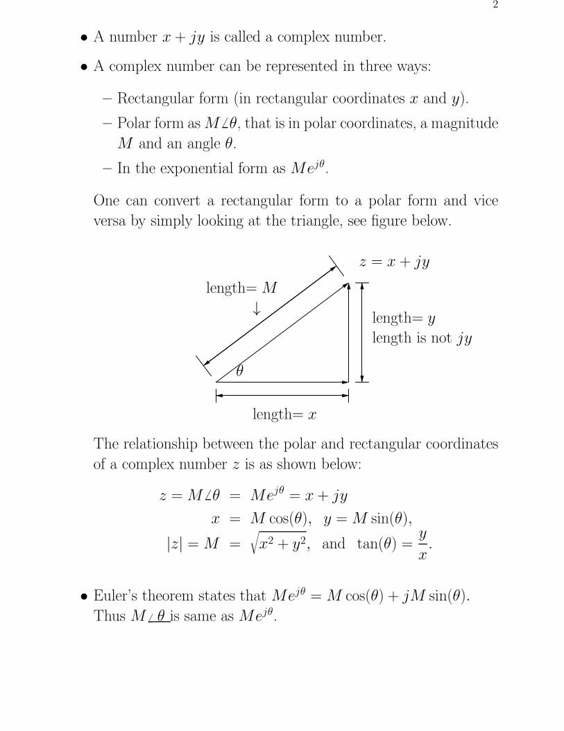
• A number x + jy is called a complex number.
• A complex number can be represented in three ways:
– Rectangular form (in rectangular coordinates x and y).
– Polar form asM 6 θ, that is in polar coordinates, a magnitude
M and an angle θ.
– In the exponential form as Mejθ.
One can convert a rectangular form to a polar form and vice
versa by simply looking at the triangle, see figure below.
θ
length= x
length= y
length is not jy
z = x + jy
length= M
↓
The relationship between the polar and rectangular coordinates
of a complex number z is as shown below:
z = M 6 θ = Mejθ = x + jy
x = M cos(θ), y = M sin(θ),
|z| = M =√
x2 + y2, and tan(θ) =y
x.
• Euler’s theorem states that Mejθ = M cos(θ) + jM sin(θ).
Thus M 6 θ is same as Mejθ.
3
Addition: Addition of two complex numbers is straight forward in
rectangular form.
(a + jb) + (c + jd) = (a + c) + j(b + d).
Subtraction: Subtraction of two complex numbers is straight for-
ward in rectangular form.
(a + jb) − (c + jd) = (a − c) + j(b − d).
Multiplication: We first show multiplication of two complex num-
bers in rectangular form.
(a + jb)(c + jd) = ac + jad + jbc + j2bd
= (ac − bd) + j(ad + bc).
We show next multiplication of two complex numbers in polar form.
Indeed
(M1ejθ1)(M2e
jθ2) = M1M2ej(θ1+θ2)
= M1M2 6 θ1 + θ2.
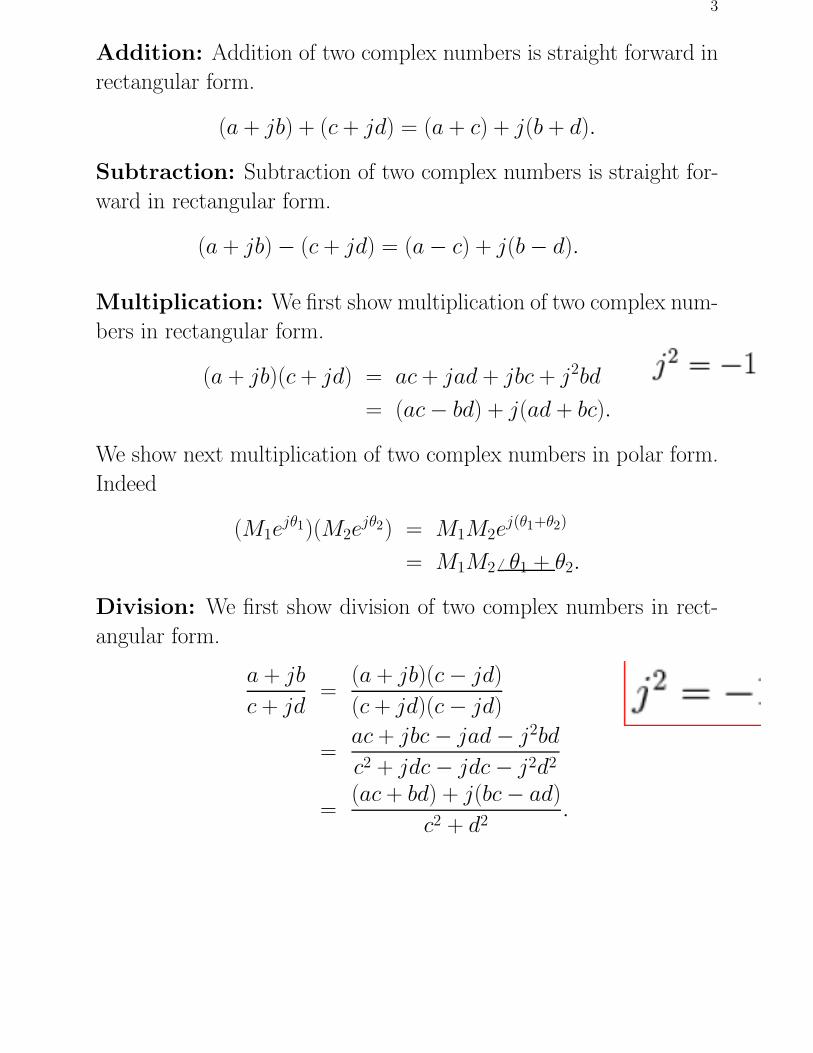
Division: We first show division of two complex numbers in rect-
angular form.
a + jb
c + jd=
(a + jb)(c − jd)
(c + jd)(c − jd)
=ac + jbc − jad − j2bd
c2 + jdc − jdc − j2d2
=(ac + bd) + j(bc − ad)
c2 + d2.
4
We show next division of two complex numbers in polar form. Indeed
M1ejθ1
M2ejθ2=
M1
M2ej(θ1−θ2) =
M1
M26 θ1 − θ2.
If z is a complex number given by z = M 6 θ = Mejθ = x + jy,
then its conjugate (denoted by z∗) is given by
z∗ = M 6 −θ = Me−jθ = x − jy.
Also,zz∗ = M 2 = x2 + y2, z + z∗ = 2x, z − z∗ = j2y.
Thusejθ + e−jθ = 2 cos(θ) and ejθ − e−jθ = 2j sin(θ).
Example: We note that
1
j=
j
j2= −j, and j = −1
j.
Example: We note that
ejπ2 = ej90
0
= j,
e−j π2 = e−j900
= −j.
Note that −j is a counterclockwise rotation of −900
or a clockwise
rotation of 900
.
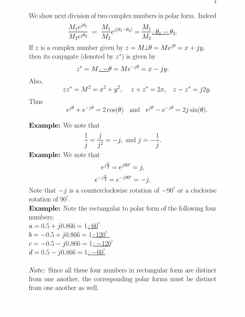
Example: Note the rectangular to polar form of the following four
numbers:
a = 0.5 + j0.866 = 1 6 600
b = −0.5 + j0.866 = 1 6 1200
c = −0.5 − j0.866 = 1 6 −1200
d = 0.5 − j0.866 = 1 6 −600
Note: Since all these four numbers in rectangular form are distinct
from one another, the corresponding polar forms must be distinct
from one another as well.
5
Example: The phasor currents in two elements connected in series
are given by I1 = M 6 600
and I2 = x+ j2.771. Find the values of x
and M .
We note that two complex numbers are equal if and only if their real
parts are equal and the imaginary parts are equal.
Also, I1 and I2 must equal each other as the given two elements are
connected in series.
Moreover, I1 = M 6 600
= M cos(600
) + jM sin(600
),
and I2 = x + j2.771.
The equality of I1 and I2 implies that
x = M cos(600
) and M sin(600
) = 2.771.
The later implies that M = 2.771sin(60
0
)= 3.2.
This enables us to calculate x = M cos(600
) = 3.2 cos(600
) = 1.6.
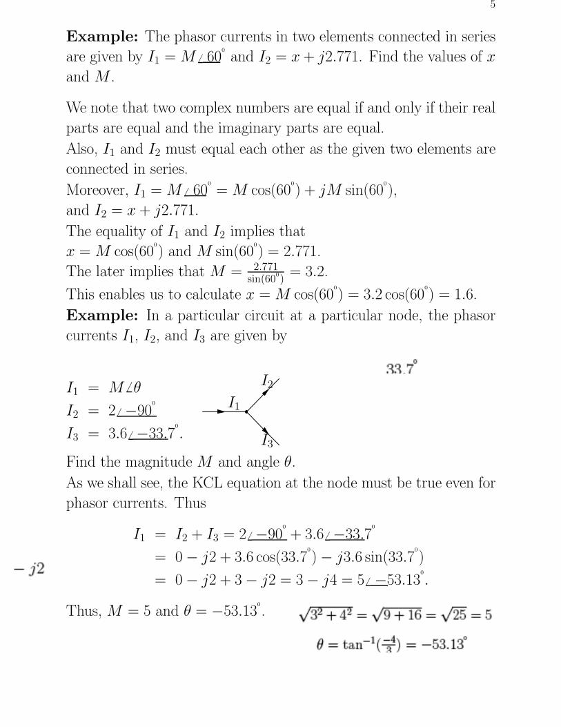
Example: In a particular circuit at a particular node, the phasor
currents I1, I2, and I3 are given by
I1 = M 6 θ
I2 = 2 6 −900
I3 = 3.6 6 −33.70
.
I1
I2
I3
Find the magnitude M and angle θ.
As we shall see, the KCL equation at the node must be true even for
phasor currents. Thus
I1 = I2 + I3 = 2 6 −900
+ 3.6 6 −33.70
= 0 − j2 + 3.6 cos(33.70
) − j3.6 sin(33.70
)
= 0 − j2 + 3 − j2 = 3 − j4 = 5 6 −53.130
.
Thus, M = 5 and θ = −53.130
.
6
Example: In any circuit, the phasor voltage V and phasor current I
of an element are related by V = IZ where Z is called the impedance
of the element.
If I = 26 6 −120.50
and Z = 3 + j4, find the voltage V .
V = IZ = 26 6 −120.50
(3 + j4) =
= 26 6 −120.50
5 6 53.10
= 130 6 −67.40
= 130 cos(−67.40
) + j130 sin(−67.40
)
= 50 − j120 volts.
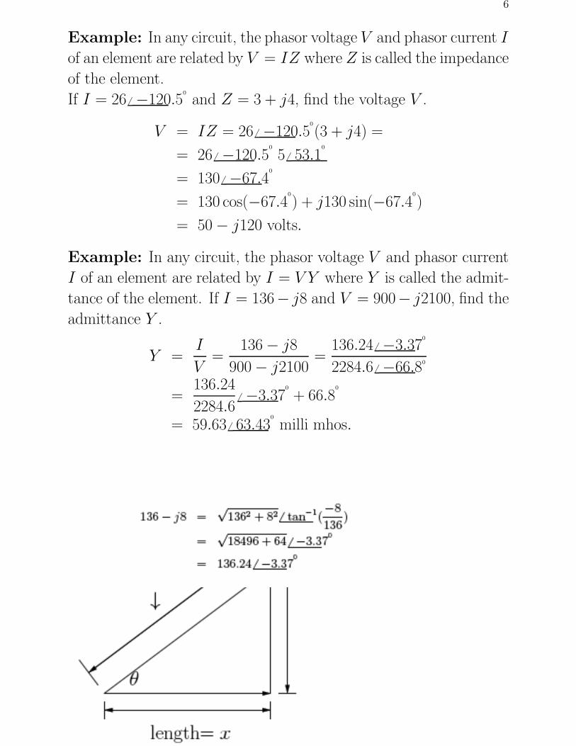
Example: In any circuit, the phasor voltage V and phasor current
I of an element are related by I = V Y where Y is called the admit-
tance of the element. If I = 136− j8 and V = 900− j2100, find the
admittance Y .
Y =I
V=
136 − j8
900 − j2100=
136.24 6 −3.370
2284.6 6 −66.80
=136.24
2284.66 −3.37
0
+ 66.80
= 59.63 6 63.430
milli mhos.

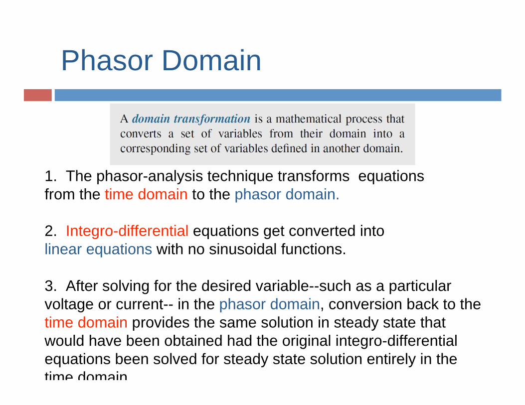
Phasor Domain
1. The phasor-analysis technique transforms equations
from the time domain to the phasor domain.
2. Integro-differential equations get converted into
linear equations with no sinusoidal functions.
3. After solving for the desired variable--such as a particular
voltage or current-- in the phasor domain, conversion back to the
time domain provides the same solution in steady state that
would have been obtained had the original integro-differential
equations been solved for steady state solution entirely in the
time domain
Principles of Electrical Engineering I
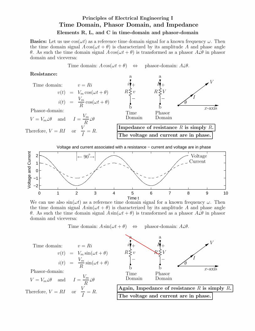
Time Domain, Phasor Domain, and ImpedanceElements R, L, and C in time-domain and phasor-domain
Basics: Let us use cos(ωt) as a reference time domain signal for a known frequency ω. Thenthe time domain signal A cos(ωt + θ) is characterized by its amplitude A and phase angleθ. As such the time domain signal A cos(ωt + θ) is transformed as a phasor A6 θ in phasordomain and viceversa:
Time domain: A cos(ωt + θ) ⇔ phasor-domain: A6 θ.
Resistance:
Time domain: v = Ri
v(t) = Vm cos(ωt + θ)
i(t) =Vm
Rcos(ωt + θ)
Phasor-domain:
V = Vm6 θ and I =
Vm
R6 θ
Therefore, V = RI orV
I= R.
b
R
−v
+
a
i
TimeDomain
b
R
−V
+
a
I
PhasorDomain
Impedance of resistance R is simply R.
The voltage and current are in phase.
V
I
θ
x-axis
0 1 2 3 4 5 6 7 8 9 10
−2
−1
0
1
2
Voltage and current associated with a resistance − current and voltage are in phase
Time t
Vol
tage
and
Cur
rent
VoltageCurrent
∣∣∣← 90
0→∣∣∣
We can use also sin(ωt) as a reference time domain signal for a known frequency ω. Thenthe time domain signal A sin(ωt + θ) is characterized by its amplitude A and phase angleθ. As such the time domain signal A sin(ωt + θ) is transformed as a phasor A6 θ in phasordomain and viceversa:
Time domain: A sin(ωt + θ) ⇔ phasor-domain: A6 θ.
Time domain: v = Ri
v(t) = Vm sin(ωt + θ)
i(t) =Vm
Rsin(ωt + θ)
Phasor-domain:
V = Vm6 θ and I =
Vm
R6 θ
Therefore, V = RI orV
I= R.
b
R
−v
+
a
i
TimeDomain
b
R
−V
+
a
I
PhasorDomain
Again, Impedance of resistance R is simply R.
The voltage and current are in phase.
V
I
θ
x-axis
2
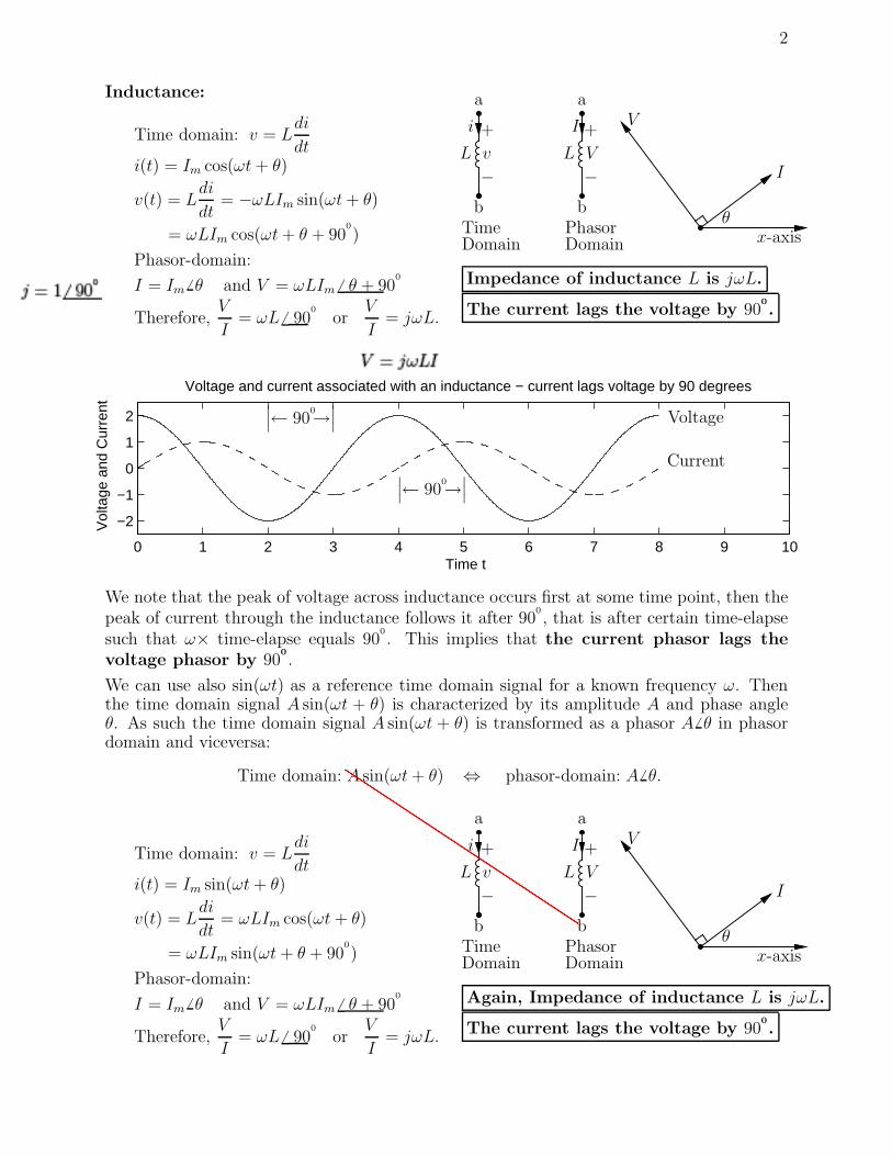
Inductance:
Time domain: v = Ldi
dt
i(t) = Im cos(ωt + θ)
v(t) = Ldi
dt= −ωLIm sin(ωt + θ)
= ωLIm cos(ωt + θ + 900
)
Phasor-domain:
I = Im6 θ and V = ωLIm 6 θ + 90
0
Therefore,V
I= ωL6 90
0
orV
I= jωL.
b
L
−v
+
a
i
TimeDomain
b
L
−V
+
a
I
PhasorDomain
Impedance of inductance L is jωL.
The current lags the voltage by 900
.
I
V
θ
x-axis
0 1 2 3 4 5 6 7 8 9 10
−2
−1
0
1
2
Voltage and current associated with an inductance − current lags voltage by 90 degrees
Time t
Vol
tage
and
Cur
rent
Voltage
Current
∣∣∣← 90
0→∣∣∣
∣∣∣← 90
0→∣∣∣
We note that the peak of voltage across inductance occurs first at some time point, then thepeak of current through the inductance follows it after 90
0
, that is after certain time-elapsesuch that ω× time-elapse equals 90
0
. This implies that the current phasor lags thevoltage phasor by 90
0
.
We can use also sin(ωt) as a reference time domain signal for a known frequency ω. Thenthe time domain signal A sin(ωt + θ) is characterized by its amplitude A and phase angleθ. As such the time domain signal A sin(ωt + θ) is transformed as a phasor A6 θ in phasordomain and viceversa:
Time domain: A sin(ωt + θ) ⇔ phasor-domain: A6 θ.
Time domain: v = Ldi
dt
i(t) = Im sin(ωt + θ)
v(t) = Ldi
dt= ωLIm cos(ωt + θ)
= ωLIm sin(ωt + θ + 900
)
Phasor-domain:
I = Im6 θ and V = ωLIm 6 θ + 90
0
Therefore,V
I= ωL6 90
0
orV
I= jωL.
b
L
−v
+
a
i
TimeDomain
b
L
−V
+
a
I
PhasorDomain
Again, Impedance of inductance L is jωL.
The current lags the voltage by 900
.
I
V
θ
x-axis
3
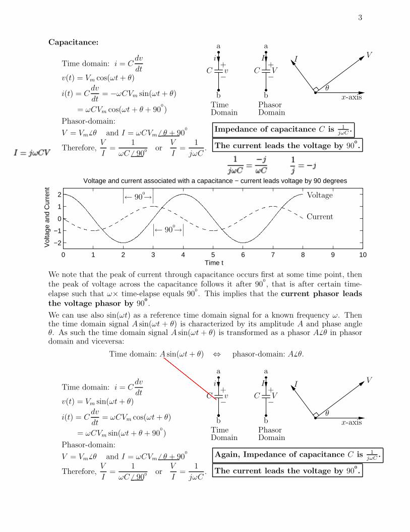
Capacitance:
Time domain: i = Cdv
dt
v(t) = Vm cos(ωt + θ)
i(t) = Cdv
dt= −ωCVm sin(ωt + θ)
= ωCVm cos(ωt + θ + 900
)
Phasor-domain:
V = Vm6 θ and I = ωCVm 6 θ + 90
0
Therefore,V
I=
1
ωC 6 900or
V
I=
1
jωC.
b
C−v
+
a
i
TimeDomain
b
C−V
+
a
I
PhasorDomain
Impedance of capacitance C is 1
jωC.
The current leads the voltage by 900
.
VI
θ
x-axis
0 1 2 3 4 5 6 7 8 9 10
−2
−1
0
1
2
Voltage and current associated with a capacitance − current leads voltage by 90 degrees
Time t
Vol
tage
and
Cur
rent
Voltage
Current
∣∣∣← 90
0→∣∣∣
∣∣∣← 90
0→∣∣∣
We note that the peak of current through capacitance occurs first at some time point, thenthe peak of voltage across the capacitance follows it after 90
0
, that is after certain time-elapse such that ω× time-elapse equals 90
0
. This implies that the current phasor leadsthe voltage phasor by 90
0
.
We can use also sin(ωt) as a reference time domain signal for a known frequency ω. Thenthe time domain signal A sin(ωt + θ) is characterized by its amplitude A and phase angleθ. As such the time domain signal A sin(ωt + θ) is transformed as a phasor A6 θ in phasordomain and viceversa:
Time domain: A sin(ωt + θ) ⇔ phasor-domain: A6 θ.
Time domain: i = Cdv
dt
v(t) = Vm sin(ωt + θ)
i(t) = Cdv
dt= ωCVm cos(ωt + θ)
= ωCVm sin(ωt + θ + 900
)
Phasor-domain:
V = Vm6 θ and I = ωCVm 6 θ + 90
0
Therefore,V
I=
1
ωC 6 900or
V
I=
1
jωC.
b
C−v
+
a
i
TimeDomain
b
C−V
+
a
I
PhasorDomain
Again, Impedance of capacitance C is 1
jωC.
The current leads the voltage by 900
.
VI
θ
x-axis
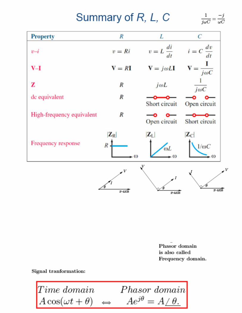
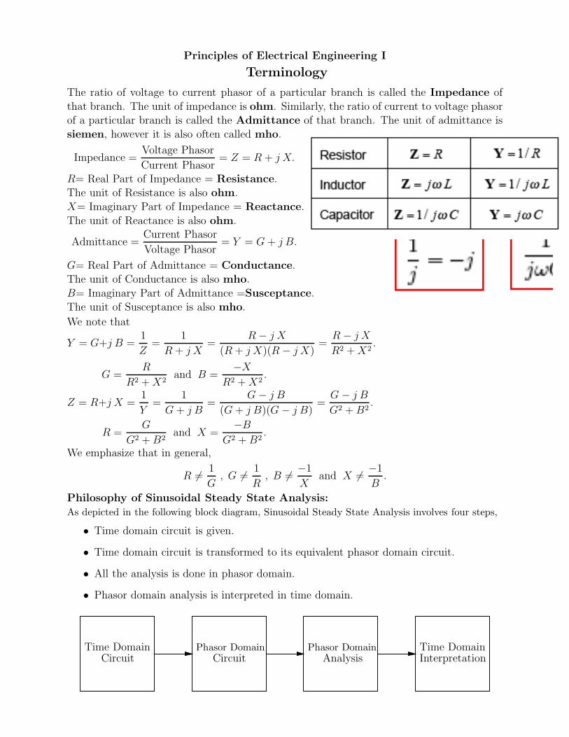
Principles of Electrical Engineering I
Terminology
The ratio of voltage to current phasor of a particular branch is called the Impedance of
that branch. The unit of impedance is ohm. Similarly, the ratio of current to voltage phasorof a particular branch is called the Admittance of that branch. The unit of admittance is
siemen, however it is also often called mho.
Impedance =Voltage Phasor
Current Phasor= Z = R + j X.
R= Real Part of Impedance = Resistance.The unit of Resistance is also ohm.
X= Imaginary Part of Impedance = Reactance.
The unit of Reactance is also ohm.
Admittance =Current Phasor
Voltage Phasor= Y = G + j B.
G= Real Part of Admittance = Conductance.The unit of Conductance is also mho.
B= Imaginary Part of Admittance =Susceptance.The unit of Susceptance is also mho.
We note that
Y = G+j B =1
Z=
1
R + j X=
R − j X
(R + j X)(R − j X)=
R − j X
R2 + X2.
G =R
R2 + X2and B =
−X
R2 + X2.
Z = R+j X =1
Y=
1
G + j B=
G − j B
(G + j B)(G − j B)=
G − j B
G2 + B2.
R =G
G2 + B2and X =
−B
G2 + B2.
We emphasize that in general,
R 6=1
G, G 6=
1
R, B 6=
−1
Xand X 6=
−1
B.
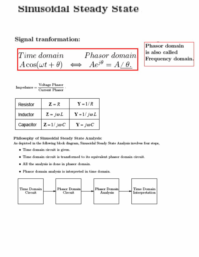
Philosophy of Sinusoidal Steady State Analysis:
As depicted in the following block diagram, Sinusoidal Steady State Analysis involves four steps,
• Time domain circuit is given.
• Time domain circuit is transformed to its equivalent phasor domain circuit.
• All the analysis is done in phasor domain.
• Phasor domain analysis is interpreted in time domain.
Time DomainCircuit
Phasor DomainCircuit
Phasor DomainAnalysis
Time DomainInterpretation
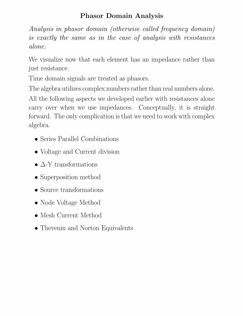
Phasor Domain Analysis
Analysis in phasor domain (otherwise called frequency domain)
is exactly the same as in the case of analysis with resistances
alone.
We visualize now that each element has an impedance rather than
just resistance.
Time domain signals are treated as phasors.
The algebra utilizes complex numbers rather than real numbers alone.
All the following aspects we developed earlier with resistances alone
carry over when we use impedances. Conceptually, it is straight
forward. The only complication is that we need to work with complex
algebra.
• Series Parallel Combinations
• Voltage and Current division
• ∆-Y transformations
• Superposition method
• Source transformations
• Node Voltage Method
• Mesh Current Method
• Thevenin and Norton Equivalents
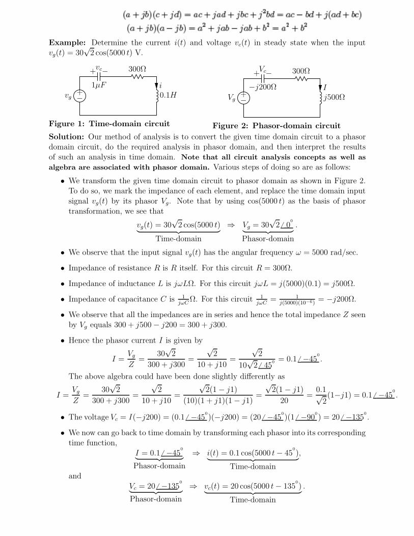
Example: Determine the current i(t) and voltage vc(t) in steady state when the inputvg(t) = 30
√2 cos(5000 t) V.
−+
vg
−vc+
1µF
300Ω
0.1Hi
Figure 1: Time-domain circuit
−+
Vg
−Vc+
−j200Ω
300Ω
j500ΩI
Figure 2: Phasor-domain circuit
Solution: Our method of analysis is to convert the given time domain circuit to a phasor
domain circuit, do the required analysis in phasor domain, and then interpret the resultsof such an analysis in time domain. Note that all circuit analysis concepts as well as
algebra are associated with phasor domain. Various steps of doing so are as follows:
• We transform the given time domain circuit to phasor domain as shown in Figure 2.To do so, we mark the impedance of each element, and replace the time domain input
signal vg(t) by its phasor Vg. Note that by using cos(5000 t) as the basis of phasor
transformation, we see that
vg(t) = 30√
2 cos(5000 t)︸ ︷︷ ︸
Time-domain
⇒ Vg = 30√
2 6 00
︸ ︷︷ ︸
Phasor-domain
.
• We observe that the input signal vg(t) has the angular frequency ω = 5000 rad/sec.
• Impedance of resistance R is R itself. For this circuit R = 300Ω.
• Impedance of inductance L is jωLΩ. For this circuit jωL = j(5000)(0.1) = j500Ω.
• Impedance of capacitance C is 1
jωCΩ. For this circuit 1
jωC= 1
j(5000)(10−6)= −j200Ω.
• We observe that all the impedances are in series and hence the total impedance Z seenby Vg equals 300 + j500 − j200 = 300 + j300.
• Hence the phasor current I is given by
I =Vg
Z=
30√
2
300 + j300=
√2
10 + j10=
√2
10√
2 6 450
= 0.1 6 −450
.
The above algebra could have been done slightly differently as
I =Vg
Z=
30√
2
300 + j300=
√2
10 + j10=
√2(1 − j1)
(10)(1 + j1)(1 − j1)=
√2(1 − j1)
20=
0.1√2(1−j1) = 0.1 6 −45
0
.
• The voltage Vc = I(−j200) = (0.1 6 −450
)(−j200) = (206 −450
)(1 6 −900
) = 20 6 −1350
.
• We now can go back to time domain by transforming each phasor into its correspondingtime function,
I = 0.1 6 −450
︸ ︷︷ ︸
Phasor-domain
⇒ i(t) = 0.1 cos(5000 t− 450
)︸ ︷︷ ︸
Time-domain
,
and
Vc = 20 6 −1350
︸ ︷︷ ︸
Phasor-domain
⇒ vc(t) = 20 cos(5000 t− 1350
)︸ ︷︷ ︸
Time-domain
.
Example: Determine the current i2 through R2 if
R1 = 10Ω, R2 = 30Ω, L = 2 µH, and C = 10 nF.
Note carefully the notations µ and n.
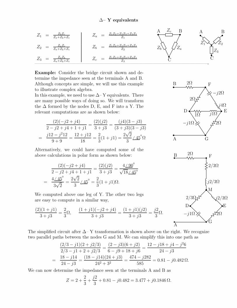
∆– Y equivalents
Z1 = ZbZc
Za+Zb+ZcZa = Z1Z2+Z2Z3+Z3Z1
Z1
Z2 = ZaZc
Za+Zb+ZcZb = Z1Z2+Z2Z3+Z3Z1
Z2
Z3 = ZaZb
Za+Zb+ZcZc = Z1Z2+Z2Z3+Z3Z1
Z3
A B
C
Zb Za
Zc A B
C
Z1 Z2
Z3
——————————————————————————————————————-
Example: Consider the bridge circuit shown and de-termine the impedance seen at the terminals A and B.Although concepts are simple, we will use this exampleto illustrate complex algebra.In this example, we need to use ∆– Y equivalents. Thereare many possible ways of doing so. We will transformthe ∆ formed by the nodes D, E, and F into a Y. Therelevant computations are as shown below:
(2)(−j2 + j4)
2 − j2 + j4 + 1 + j1=
(2)(j2)
3 + j3=
(j4)(3 − j3)
(3 + j3)(3 − j3)
=j12 − j
212
9 + 9=
12 + j12
18=
2
3(1 + j1) =
2√
2
36 45
0
Ω
Alternatively, we could have computed some of theabove calculations in polar form as shown below:
(2)(−j2 + j4)
2 − j2 + j4 + 1 + j1=
(2)(j2)
3 + j3=
4 6 900
√18 6 450
=4 6 45
0
3√
2=
2√
2
36 45
0
=2
3(1 + j1)Ω.
We computed above one leg of Y. The other two legsare easy to compute in a similar way,
(2)(1 + j1)
3 + j3=
2
3Ω,
(1 + j1)(−j2 + j4)
3 + j3=
(1 + j1)(j2)
3 + j3=
j2
3Ω.
A
B F
G
2Ω
j4Ω
−j2Ω
2Ω
2Ω
E
−j1Ω
D1Ω j1Ω
A
B F2Ω
G
−j1Ω
D
2Ω
E
2/3Ω j2/3Ω
M
j2/3Ω
2/3Ω
The simplified circuit after ∆– Y transformation is shown above on the right. We recognizetwo parallel paths between the nodes G and M. We can simplify this into one path as
(2/3 − j1)(2 + j2/3)
2/3 − j1 + 2 + j2/3=
(2 − j3)(6 + j2)
6 − j9 + 18 + j6=
12 − j18 + j4 − j26
24 − j3
=18 − j14
24 − j3=
(18 − j14)(24 + j3)
242 + 32=
474 − j282
585= 0.81 − j0.482 Ω.
We can now determine the impedance seen at the terminals A and B as
Z = 2 +2
3+
j2
3+ 0.81 − j0.482 = 3.477 + j0.1846 Ω.
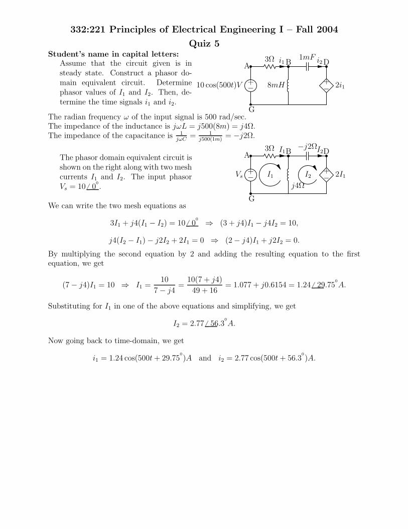
332:221 Principles of Electrical Engineering I – Fall 2004
Quiz 5Student’s name in capital letters:
Assume that the circuit given is insteady state. Construct a phasor do-main equivalent circuit. Determinephasor values of I1 and I2. Then, de-termine the time signals i1 and i2.
8mH
B1mF
D
G
3Ω
−+10 cos(500t)V
A
−+ 2i1
i1 i2
The radian frequency ω of the input signal is 500 rad/sec.The impedance of the inductance is jωL = j500(8m) = j4Ω.The impedance of the capacitance is 1
jωC= 1
j500(1m)= −j2Ω.
The phasor domain equivalent circuit isshown on the right along with two meshcurrents I1 and I2. The input phasorVs = 10 6 0
0
.
B
j4Ω
−j2ΩD
G
3Ω
−+
Vs
A
−+ 2I1
I1 I2
I2I1
We can write the two mesh equations as
3I1 + j4(I1 − I2) = 10 6 00
⇒ (3 + j4)I1 − j4I2 = 10,
j4(I2 − I1) − j2I2 + 2I1 = 0 ⇒ (2 − j4)I1 + j2I2 = 0.
By multiplying the second equation by 2 and adding the resulting equation to the firstequation, we get
(7 − j4)I1 = 10 ⇒ I1 =10
7 − j4=
10(7 + j4)
49 + 16= 1.077 + j0.6154 = 1.24 6 29.75
0
A.
Substituting for I1 in one of the above equations and simplifying, we get
I2 = 2.77 6 56.30
A.
Now going back to time-domain, we get
i1 = 1.24 cos(500t + 29.750
)A and i2 = 2.77 cos(500t + 56.30
)A.
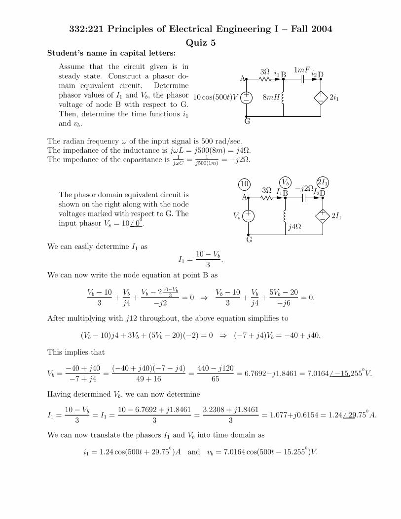
332:221 Principles of Electrical Engineering I – Fall 2004
Quiz 5Student’s name in capital letters:
Assume that the circuit given is insteady state. Construct a phasor do-main equivalent circuit. Determinephasor values of I1 and Vb, the phasorvoltage of node B with respect to G.Then, determine the time functions i1
and vb.
8mH
B1mF
D
G
3Ω
−+10 cos(500t)V
A
−+ 2i1
i1 i2
The radian frequency ω of the input signal is 500 rad/sec.The impedance of the inductance is jωL = j500(8m) = j4Ω.The impedance of the capacitance is 1
jωC= 1
j500(1m)= −j2Ω.
The phasor domain equivalent circuit isshown on the right along with the nodevoltages marked with respect to G. Theinput phasor Vs = 10 6 0
0
.
B
Vb
j4Ω
−j2ΩD
2I1
G
3Ω
−+
Vs
A
10
−+ 2I1
I1 I2
We can easily determine I1 as
I1 =10 − Vb
3.
We can now write the node equation at point B as
Vb − 10
3+
Vb
j4+
Vb − 210−Vb
3
−j2= 0 ⇒
Vb − 10
3+
Vb
j4+
5Vb − 20
−j6= 0.
After multiplying with j12 throughout, the above equation simplifies to
(Vb − 10)j4 + 3Vb + (5Vb − 20)(−2) = 0 ⇒ (−7 + j4)Vb = −40 + j40.
This implies that
Vb =−40 + j40
−7 + j4=
(−40 + j40)(−7 − j4)
49 + 16=
440 − j120
65= 6.7692−j1.8461 = 7.0164 6 −15.255
0
V.
Having determined Vb, we can now determine
I1 =10 − Vb
3= I1 =
10 − 6.7692 + j1.8461
3=
3.2308 + j1.8461
3= 1.077+j0.6154 = 1.24 6 29.75
0
A.
We can now translate the phasors I1 and Vb into time domain as
i1 = 1.24 cos(500t + 29.750
)A and vb = 7.0164 cos(500t− 15.2550
)V.
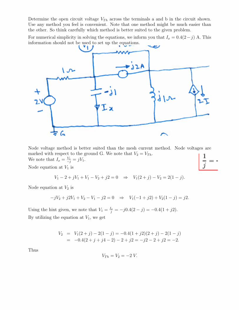
Determine the open circuit voltage VTh across the terminals a and b in the circuit shown.Use any method you feel is convenient. Note that one method might be much easier thanthe other. So think carefully which method is better suited to the given problem.
For numerical simplicity in solving the equations, we inform you that Ix = 0.4(2− j) A. Thisinformation should not be used to set up the equations.
Node voltage method is better suited than the mesh current method. Node voltages aremarked with respect to the ground G. We note that V2 = VTh.We note that Ix = V1
−j= jV1.
Node equation at V1 is
V1 − 2 + jV1 + V1 − V2 + j2 = 0 ⇒ V1(2 + j)− V2 = 2(1− j).
Node equation at V2 is
−jV2 + j2V1 + V2 − V1 − j2 = 0 ⇒ V1(−1 + j2) + V2(1− j) = j2.
Using the hint given, we note that V1 = Ixj
= −j0.4(2− j) = −0.4(1 + j2).
By utilizing the equation at V1, we get
V2 = V1(2 + j)− 2(1− j) = −0.4(1 + j2)(2 + j)− 2(1− j)
= −0.4(2 + j + j4− 2)− 2 + j2 = −j2− 2 + j2 = −2.
ThusVTh = V2 = −2 V.
2
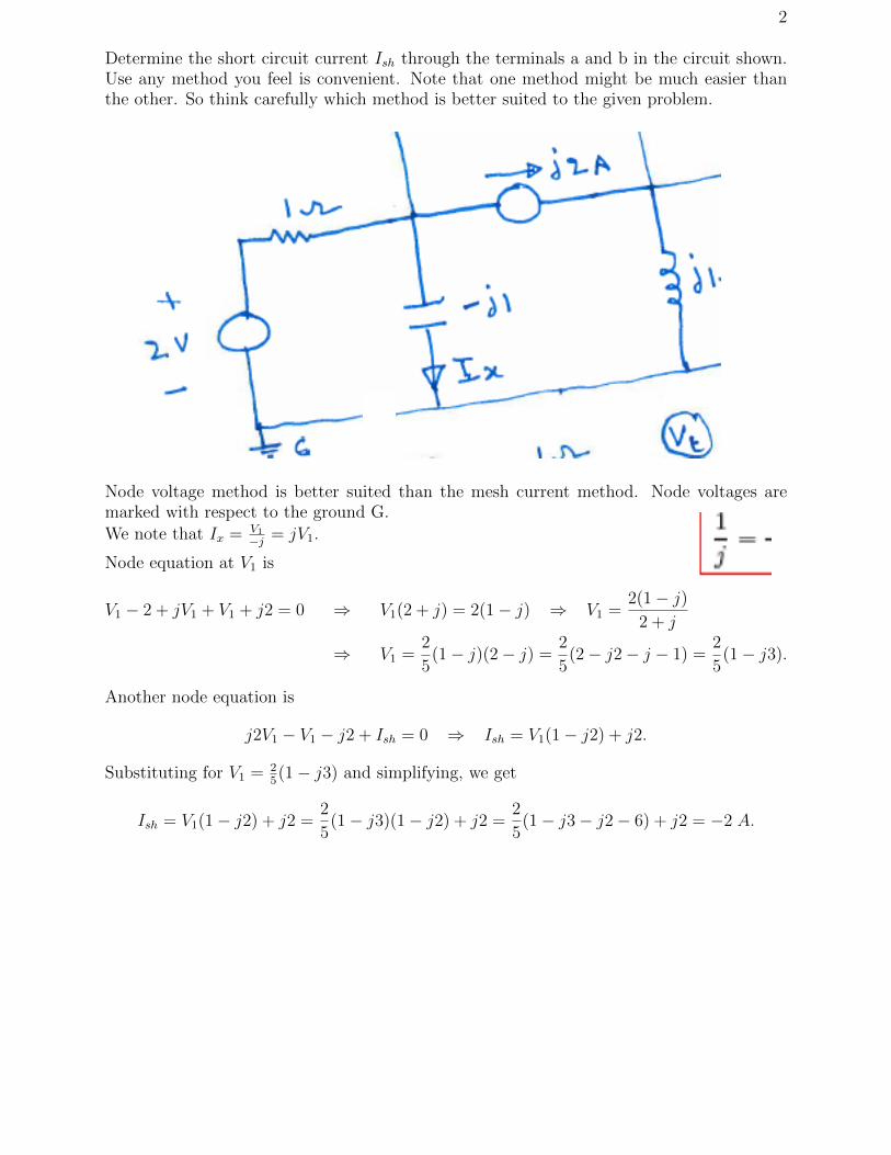
Determine the short circuit current Ish through the terminals a and b in the circuit shown.Use any method you feel is convenient. Note that one method might be much easier thanthe other. So think carefully which method is better suited to the given problem.
Node voltage method is better suited than the mesh current method. Node voltages aremarked with respect to the ground G.We note that Ix = V1
−j= jV1.
Node equation at V1 is
V1 − 2 + jV1 + V1 + j2 = 0 ⇒ V1(2 + j) = 2(1− j) ⇒ V1 =2(1− j)
2 + j
⇒ V1 =2
5(1− j)(2− j) =
2
5(2− j2− j − 1) =
2
5(1− j3).
Another node equation is
j2V1 − V1 − j2 + Ish = 0 ⇒ Ish = V1(1− j2) + j2.
Substituting for V1 = 25(1− j3) and simplifying, we get
Ish = V1(1− j2) + j2 =2
5(1− j3)(1− j2) + j2 =
2
5(1− j3− j2− 6) + j2 = −2 A.
3
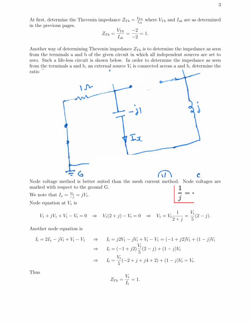
At first, determine the Thevenin impedance ZTh = VTh
Ishwhere VTh and Ish are as determined
in the previous pages.
ZTh =VTh
Ish=−2
−2= 1.
Another way of determining Thevenin impedance ZTh is to determine the impedance as seenfrom the terminals a and b of the given circuit in which all independent sources are set tozero. Such a life-less circuit is shown below. In order to determine the impedance as seenfrom the terminals a and b, an external source Vt is connected across a and b, determine theratio Vt
It.
Node voltage method is better suited than the mesh current method. Node voltages aremarked with respect to the ground G.
We note that Ix = V1
−j= jV1.
Node equation at V1 is
V1 + jV1 + V1 − Vt = 0 ⇒ V1(2 + j)− Vt = 0 ⇒ V1 = Vt1
2 + j=
Vt
5(2− j).
Another node equation is
It = 2Ix − jVt + Vt − V1 ⇒ It = j2V1 − jVt + Vt − V1 = (−1 + j2)V1 + (1− j)Vt
⇒ It = (−1 + j2)Vt
5(2− j) + (1− j)Vt
⇒ It =Vt
5(−2 + j + j4 + 2) + (1− j)Vt = Vt.
Thus
ZTh =Vt
It= 1.
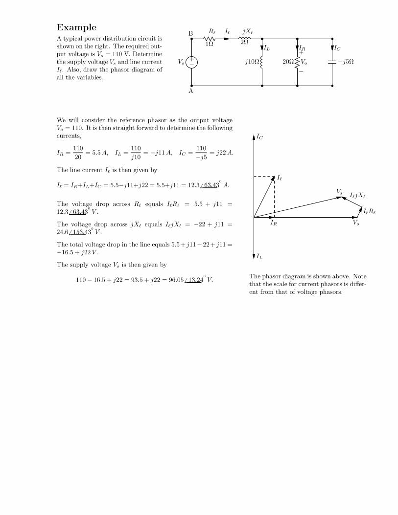
ExampleA typical power distribution circuit isshown on the right. The required out-put voltage is Vo = 110 V. Determinethe supply voltage Vs and line currentIℓ. Also, draw the phasor diagram ofall the variables.
−+Vs
1Ω 2Ω
j10Ω −j5Ω20Ω
−Vo
+IL IR IC
IℓRℓ jXℓ
A
B
We will consider the reference phasor as the output voltageVo = 110. It is then straight forward to determine the followingcurrents,
IR =110
20= 5.5 A, IL =
110
j10= −j11 A, IC =
110
−j5= j22 A.
The line current Iℓ is then given by
Iℓ = IR+IL+IC = 5.5−j11+j22 = 5.5+j11 = 12.3 6 63.430
A.
The voltage drop across Rℓ equals IℓRℓ = 5.5 + j11 =12.3 6 63.43
0
V .
The voltage drop across jXℓ equals IℓjXℓ = −22 + j11 =24.6 6 153.43
0
V .
The total voltage drop in the line equals 5.5+ j11−22+ j11 =−16.5 + j22 V .
The supply voltage Vs is then given by
110 − 16.5 + j22 = 93.5 + j22 = 96.05 6 13.240
V.
IR
IL
IC
Iℓ
Vo
IℓRℓ
IℓjXℓ
Vs
The phasor diagram is shown above. Notethat the scale for current phasors is differ-ent from that of voltage phasors.
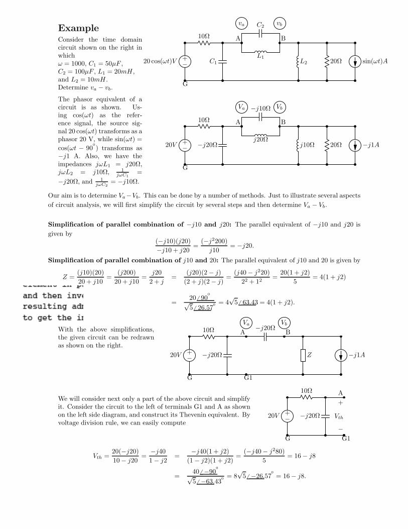
ExampleConsider the time domaincircuit shown on the right inwhichω = 1000, C1 = 50µF ,C2 = 100µF , L1 = 20mH ,and L2 = 10mH .Determine va − vb.
−+20 cos(ωt)V
10Ω
C1
C2
L1
va vb
L2 20Ω sin(ωt)A
G
A B
The phasor equivalent of acircuit is as shown. Us-ing cos(ωt) as the refer-ence signal, the source sig-nal 20 cos(ωt) transforms as aphasor 20 V, while sin(ωt) =
cos(ωt − 900
) transforms as−j1 A. Also, we have theimpedances jωL1 = j20Ω,jωL2 = j10Ω, 1
jωC1
=
−j20Ω, and 1
jωC2
= −j10Ω.
−+20V
10Ω
−j20Ω
−j10Ω
j20Ω
Va Vb
j10Ω 20Ω −j1A
G
A B
Our aim is to determine Va−Vb. This can be done by a number of methods. Just to illustrate several aspects
of circuit analysis, we will first simplify the circuit by several steps and then determine Va − Vb.
Simplification of parallel combination of −j10 and j20: The parallel equivalent of −j10 and j20 is
given by(−j10)(j20)−j10 + j20
=(−j2200)
j10= −j20.
Simplification of parallel combination of j10 and 20: The parallel equivalent of j10 and 20 is given by
Z =(j10)(20)
20 + j10=
(j200)
20 + j10=
j20
2 + j=
(j20)(2− j)
(2 + j)(2− j)=
(j40− j220)
22 + 12=
20(1 + j2)
5= 4(1 + j2)
=20 6 90
0
√56 26.57
0= 4√56 63.43 = 4(1 + j2).
With the above simplifications,the given circuit can be redrawnas shown on the right.
−+20V
10Ω
−j20Ω
Va −j20ΩVb
Z −j1A
G
A B
G1
We will consider next only a part of the above circuit and simplifyit. Consider the circuit to the left of terminals G1 and A as shownon the left side diagram, and construct its Thevenin equivalent. Byvoltage division rule, we can easily compute
−+20V
10Ω
−j20Ω
G
A
Vth
+
−G1
Vth =20(−j20)10− j20
=−j401− j2
=−j40(1 + j2)
(1− j2)(1 + j2)=
(−j40− j280)
5= 16− j8
=40 6 −900
√5 6 −63.430
= 8√56 −26.570
= 16− j8.
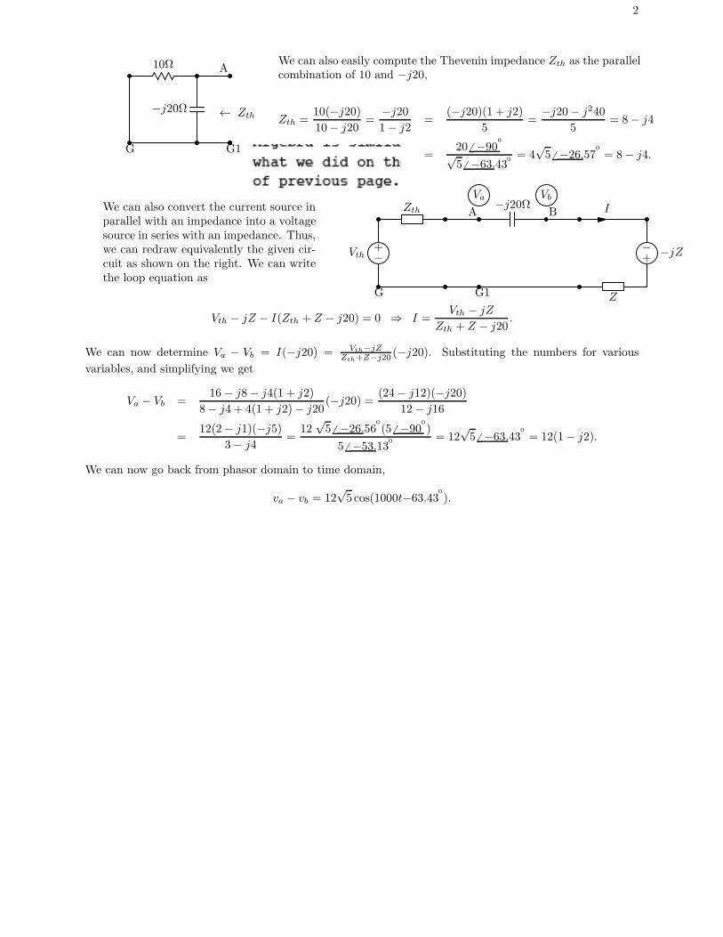
2
10Ω
−j20Ω
G
A
← Zth
G1
We can also easily compute the Thevenin impedance Zth as the parallelcombination of 10 and −j20,
Zth =10(−j20)10− j20
=−j201− j2
=(−j20)(1 + j2)
5=−j20− j240
5= 8− j4
=20 6 −900
√56 −63.430
= 4√5 6 −26.570
= 8− j4.
We can also convert the current source inparallel with an impedance into a voltagesource in series with an impedance. Thus,we can redraw equivalently the given cir-cuit as shown on the right. We can writethe loop equation as
−+
Vth
Zth
Va −j20ΩVb
Z
−+ −jZ
I
G
A B
G1
Vth − jZ − I(Zth + Z − j20) = 0 ⇒ I =Vth − jZ
Zth + Z − j20.
We can now determine Va − Vb = I(−j20) = Vth−jZZth+Z−j20
(−j20). Substituting the numbers for various
variables, and simplifying we get
Va − Vb =16− j8− j4(1 + j2)
8− j4 + 4(1 + j2)− j20(−j20) = (24− j12)(−j20)
12− j16
=12(2− j1)(−j5)
3− j4=
12√5 6 −26.560
(5 6 −900
)
5 6 −53.130= 12
√5 6 −63.430
= 12(1− j2).
We can now go back from phasor domain to time domain,
va − vb = 12√5 cos(1000t−63.430
).
3
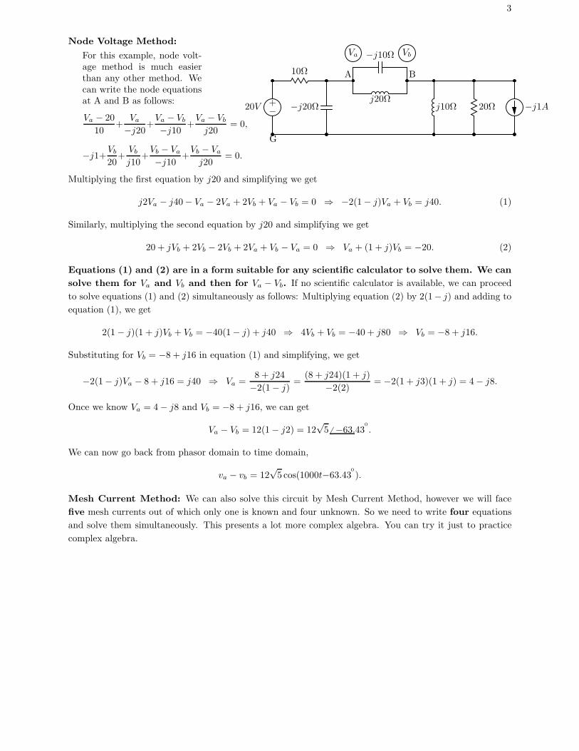
Node Voltage Method:
For this example, node volt-age method is much easierthan any other method. Wecan write the node equationsat A and B as follows:
Va − 20
10+
Va
−j20+Va − Vb
−j10 +Va − Vb
j20= 0,
−j1+Vb
20+
Vb
j10+Vb − Va
−j10 +Vb − Va
j20= 0.
−+20V
10Ω
−j20Ω
−j10Ω
j20Ω
Va Vb
j10Ω 20Ω −j1A
G
A B
Multiplying the first equation by j20 and simplifying we get
j2Va − j40− Va − 2Va + 2Vb + Va − Vb = 0 ⇒ −2(1− j)Va + Vb = j40. (1)
Similarly, multiplying the second equation by j20 and simplifying we get
20 + jVb + 2Vb − 2Vb + 2Va + Vb − Va = 0 ⇒ Va + (1 + j)Vb = −20. (2)
Equations (1) and (2) are in a form suitable for any scientific calculator to solve them. We can
solve them for Va and Vb and then for Va − Vb. If no scientific calculator is available, we can proceed
to solve equations (1) and (2) simultaneously as follows: Multiplying equation (2) by 2(1− j) and adding to
equation (1), we get
2(1− j)(1 + j)Vb + Vb = −40(1− j) + j40 ⇒ 4Vb + Vb = −40 + j80 ⇒ Vb = −8 + j16.
Substituting for Vb = −8 + j16 in equation (1) and simplifying, we get
−2(1− j)Va − 8 + j16 = j40 ⇒ Va =8 + j24
−2(1− j)=
(8 + j24)(1 + j)
−2(2) = −2(1 + j3)(1 + j) = 4− j8.
Once we know Va = 4− j8 and Vb = −8 + j16, we can get
Va − Vb = 12(1− j2) = 12√5 6 −63.430
.
We can now go back from phasor domain to time domain,
va − vb = 12√5 cos(1000t−63.430
).
Mesh Current Method: We can also solve this circuit by Mesh Current Method, however we will face
five mesh currents out of which only one is known and four unknown. So we need to write four equations
and solve them simultaneously. This presents a lot more complex algebra. You can try it just to practice
complex algebra.
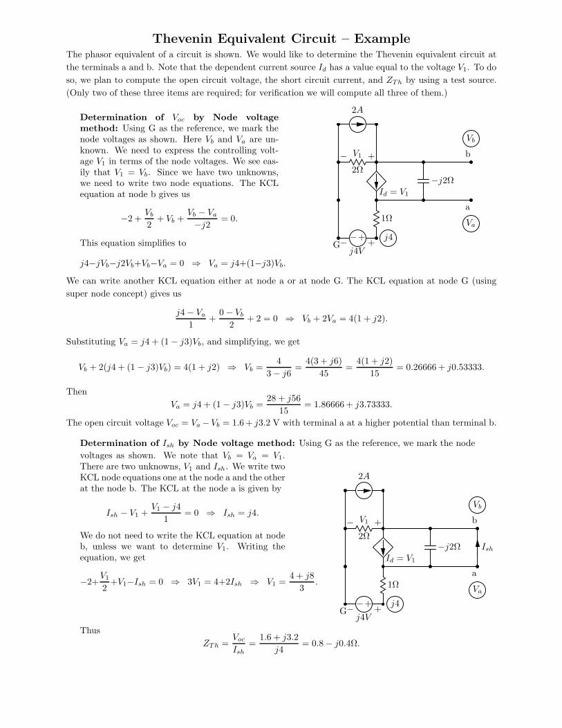
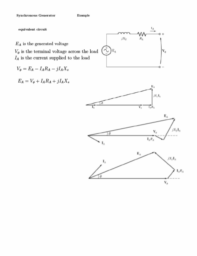
Thevenin Equivalent Circuit – ExampleThe phasor equivalent of a circuit is shown. We would like to determine the Thevenin equivalent circuit at
the terminals a and b. Note that the dependent current source Id has a value equal to the voltage V1. To do
so, we plan to compute the open circuit voltage, the short circuit current, and ZTh by using a test source.
(Only two of these three items are required; for verification we will compute all three of them.)
Determination of Voc by Node voltage
method: Using G as the reference, we mark thenode voltages as shown. Here Vb and Va are un-known. We need to express the controlling volt-age V1 in terms of the node voltages. We see eas-ily that V1 = Vb. Since we have two unknowns,we need to write two node equations. The KCLequation at node b gives us
−2 +Vb
2+ Vb +
Vb − Va
−j2= 0.
This equation simplifies to
j4−jVb−j2Vb+Vb−Va = 0 ⇒ Va = j4+(1−j3)Vb.
−+−j4V
+j4
1Ω
2Ω
− V1 +
2A
−j2Ω
Vb
Va
G
a
b
Id = V1
We can write another KCL equation either at node a or at node G. The KCL equation at node G (using
super node concept) gives us
j4 − Va
1+
0 − Vb
2+ 2 = 0 ⇒ Vb + 2Va = 4(1 + j2).
Substituting Va = j4 + (1 − j3)Vb, and simplifying, we get
Vb + 2(j4 + (1 − j3)Vb) = 4(1 + j2) ⇒ Vb =4
3 − j6=
4(3 + j6)
45=
4(1 + j2)
15= 0.26666 + j0.53333.
Then
Va = j4 + (1 − j3)Vb =28 + j56
15= 1.86666 + j3.73333.
The open circuit voltage Voc = Va −Vb = 1.6 + j3.2 V with terminal a at a higher potential than terminal b.
Determination of Ish by Node voltage method: Using G as the reference, we mark the node
voltages as shown. We note that Vb = Va = V1.There are two unknowns, V1 and Ish. We write twoKCL node equations one at the node a and the otherat the node b. The KCL at the node a is given by
Ish − V1 +V1 − j4
1= 0 ⇒ Ish = j4.
We do not need to write the KCL equation at nodeb, unless we want to determine V1. Writing theequation, we get
−2+V1
2+V1−Ish = 0 ⇒ 3V1 = 4+2Ish ⇒ V1 =
4 + j8
3.
−+−j4V
+j4
1Ω
2Ω
− V1 +
2A
−j2Ω
Vb
Va
G
a
b
Id = V1
Ish
Thus
ZTh =Voc
Ish
=1.6 + j3.2
j4= 0.8 − j0.4Ω.

2
Determination of ZTh by using a test source: Theindependent sources are set to zero, i.e the current sourceis opened and the voltage source is shorted. The resultingcircuit is shown on the right where a test voltage of 1 Vbetween the terminals b and a is applied. It is easy tocompute V1 as − 2
3V . Knowing V1, we can easily compute
Itest as
Itest =1
−j2+
1
3+
2
3= 1 + j0.5A.
Thus
ZTh =1
1 + j0.5= 0.8 − j0.4Ω.
Itest
1Ω
2Ω
− V1 +
−j2Ω
G
a
b
Id = V1
−+ 1V
Determination of Voc by Mesh current method:
Just for illustration, we used source transformation, andredrew the given circuit as shown while marking all themesh currents in it. Here I1 and I2 are unknown. Weneed to express the controlling voltage V1 in terms ofthe mesh currents. We see easily that controlling voltageV1 = 2(I1 + 2). The dependent current source Id hasa value equal to the voltage V1. On the other hand, interms of the chosen mesh currents Id = −(I1+I2). Thus,we get the relationship,
Id = −(I1+I2) = V1 = 2(I1+2) ⇒ −(I1+I2) = 2(I1+2).
We need one more equation. The KVL equation HKNR-SPH gives us
2(I1 + 2) + j2I2 − (j4 − I1) = 0.
j4A
1Ω
2Ω
− V1 +
2A
−j2Ω
G
a
b
H
K
L M
N
Q
P
R
S
Id = V1
I1I2
2A
j4A
By solving the above equations, we get
I1 =−5.6 + j0.8
3and I2 = 1.6 − j0.8.
Thus, the open circuit voltage Voc = j2I2 = 1.6+ j3.2V with the terminal a being at a higher potential than
the terminal b.
Determination of Ish by Mesh current method:
Just for illustration, we used source transformation, andredrew the given circuit as shown while marking all themesh currents in it. Here I1, I2, and Ish are unknown.We need to express the controlling voltage V1 in termsof the mesh currents. We see easily that V1 = 2(I1 + 2).The dependent current source V1 can be related to themesh currents as
V1 = 2(I1 + 2) = −(I1 + I2).
We need two more equations. The KVL equation HKN-RbaSPH gives us
2(I1 + 2) − (j4 − I1) = 0.
The KVL equation RbaSR gives us
−j2(I2 + Ish) = 0.
j4A
1Ω
2Ω
− V1 +
2A
−j2Ω
G
a
b
H
K
L M
N
Q
P
R
S
Id = V1
I1I2
2A
j4A
Ish Ish
Solving the above equations, we get 3I1 = −4 + j4 A, I2 = −Ish, and Ish = j4 A.
332:221 Principles of Electrical Engineering I
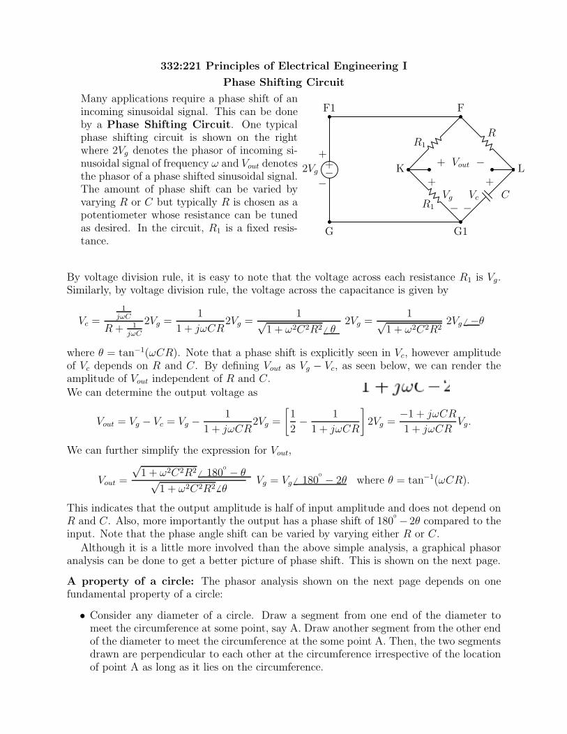
Phase Shifting Circuit
Many applications require a phase shift of anincoming sinusoidal signal. This can be doneby a Phase Shifting Circuit. One typicalphase shifting circuit is shown on the rightwhere 2Vg denotes the phasor of incoming si-nusoidal signal of frequency ω and Vout denotesthe phasor of a phase shifted sinusoidal signal.The amount of phase shift can be varied byvarying R or C but typically R is chosen as apotentiometer whose resistance can be tunedas desired. In the circuit, R1 is a fixed resis-tance.
−
+Vg
−
+Vc
−+
−2Vg
++ Vout −
G
F1 F
K L
G1
R1
C
R1
R
By voltage division rule, it is easy to note that the voltage across each resistance R1 is Vg.Similarly, by voltage division rule, the voltage across the capacitance is given by
Vc =1
jωC
R + 1
jωC
2Vg =1
1 + jωCR2Vg =
1√1 + ω2C2R2
6 θ2Vg =
1√1 + ω2C2R2
2Vg 6 −θ
where θ = tan−1(ωCR). Note that a phase shift is explicitly seen in Vc, however amplitudeof Vc depends on R and C. By defining Vout as Vg − Vc, as seen below, we can render theamplitude of Vout independent of R and C.
We can determine the output voltage as
Vout = Vg − Vc = Vg −1
1 + jωCR2Vg =
[
1
2−
1
1 + jωCR
]
2Vg =−1 + jωCR
1 + jωCRVg.
We can further simplify the expression for Vout,
Vout =
√1 + ω2C2R2
6 1800 − θ√
1 + ω2C2R26 θ
Vg = Vg 6 1800
− 2θ where θ = tan−1(ωCR).
This indicates that the output amplitude is half of input amplitude and does not depend onR and C. Also, more importantly the output has a phase shift of 180
0 − 2θ compared to theinput. Note that the phase angle shift can be varied by varying either R or C.
Although it is a little more involved than the above simple analysis, a graphical phasoranalysis can be done to get a better picture of phase shift. This is shown on the next page.
A property of a circle: The phasor analysis shown on the next page depends on onefundamental property of a circle:
• Consider any diameter of a circle. Draw a segment from one end of the diameter tomeet the circumference at some point, say A. Draw another segment from the other endof the diameter to meet the circumference at the some point A. Then, the two segmentsdrawn are perpendicular to each other at the circumference irrespective of the locationof point A as long as it lies on the circumference.
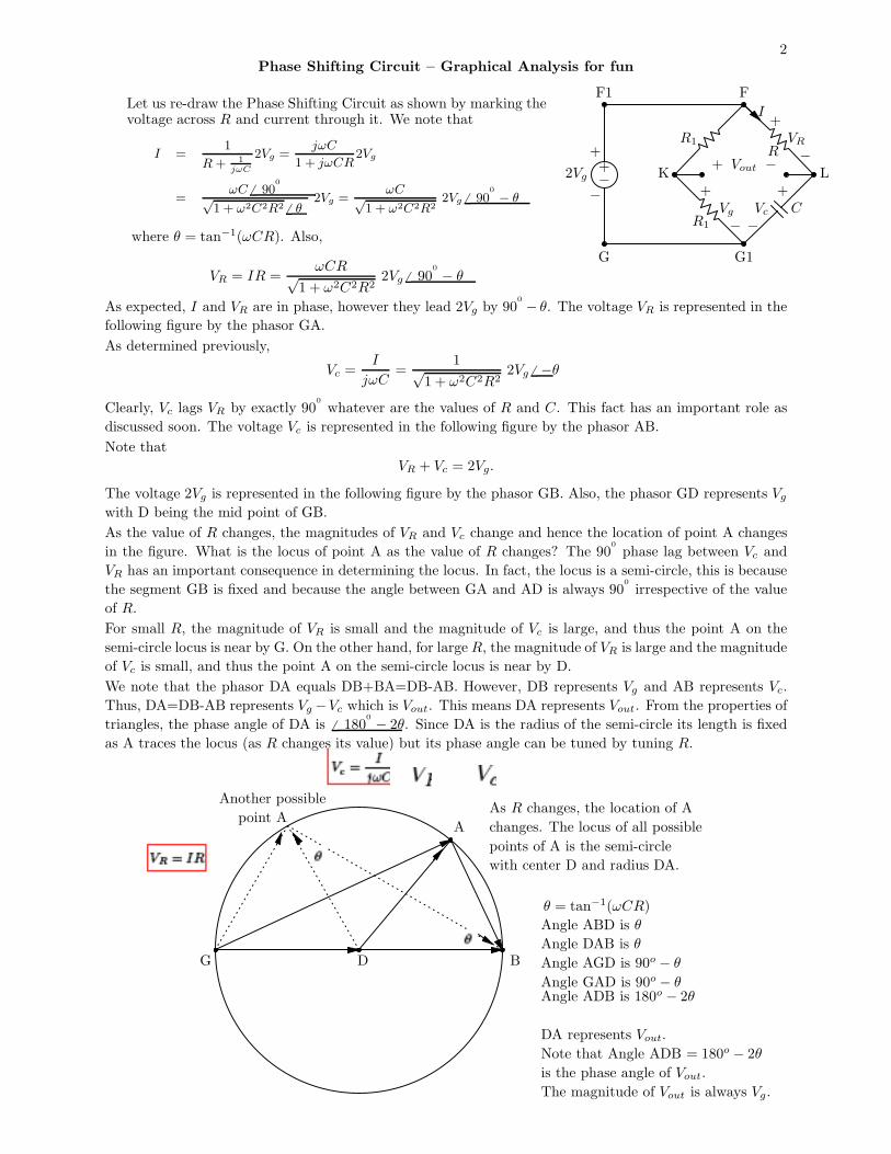
2Phase Shifting Circuit – Graphical Analysis for fun
Let us re-draw the Phase Shifting Circuit as shown by marking thevoltage across R and current through it. We note that
I =1
R +1
jωC
2Vg =jωC
1 + jωCR2Vg
=ωC 6 90
0
√
1 + ω2C2R26 θ
2Vg =ωC
√
1 + ω2C2R22Vg 6 90
0
− θ
where θ = tan−1(ωCR). Also,
VR = IR =ωCR
√1 + ω2C2R2
2Vg 6 900
− θ
−
+Vg
−
+Vc
−
+VR
I
−+
−2Vg
++ Vout −
G
F1 F
K L
G1
R1
C
R1
R
As expected, I and VR are in phase, however they lead 2Vg by 900
− θ. The voltage VR is represented in the
following figure by the phasor GA.
As determined previously,
Vc =I
jωC=
1√
1 + ω2C2R22Vg 6 −θ
Clearly, Vc lags VR by exactly 900
whatever are the values of R and C. This fact has an important role as
discussed soon. The voltage Vc is represented in the following figure by the phasor AB.
Note that
VR + Vc = 2Vg.
The voltage 2Vg is represented in the following figure by the phasor GB. Also, the phasor GD represents Vg
with D being the mid point of GB.
As the value of R changes, the magnitudes of VR and Vc change and hence the location of point A changes
in the figure. What is the locus of point A as the value of R changes? The 900
phase lag between Vc and
VR has an important consequence in determining the locus. In fact, the locus is a semi-circle, this is because
the segment GB is fixed and because the angle between GA and AD is always 900
irrespective of the value
of R.
For small R, the magnitude of VR is small and the magnitude of Vc is large, and thus the point A on the
semi-circle locus is near by G. On the other hand, for large R, the magnitude of VR is large and the magnitude
of Vc is small, and thus the point A on the semi-circle locus is near by D.
We note that the phasor DA equals DB+BA=DB-AB. However, DB represents Vg and AB represents Vc.
Thus, DA=DB-AB represents Vg −Vc which is Vout. This means DA represents Vout. From the properties of
triangles, the phase angle of DA is 6 1800
− 2θ. Since DA is the radius of the semi-circle its length is fixed
as A traces the locus (as R changes its value) but its phase angle can be tuned by tuning R.
G D B
A
As R changes, the location of A
changes. The locus of all possible
points of A is the semi-circle
with center D and radius DA.
Another possible
point A
Angle ABD is θ
Angle DAB is θ
Angle AGD is 90o − θ
Angle GAD is 90o − θAngle ADB is 180o − 2θ
DA represents Vout.
Note that Angle ADB = 180o − 2θ
is the phase angle of Vout.
The magnitude of Vout is always Vg.
θ = tan−1(ωCR)
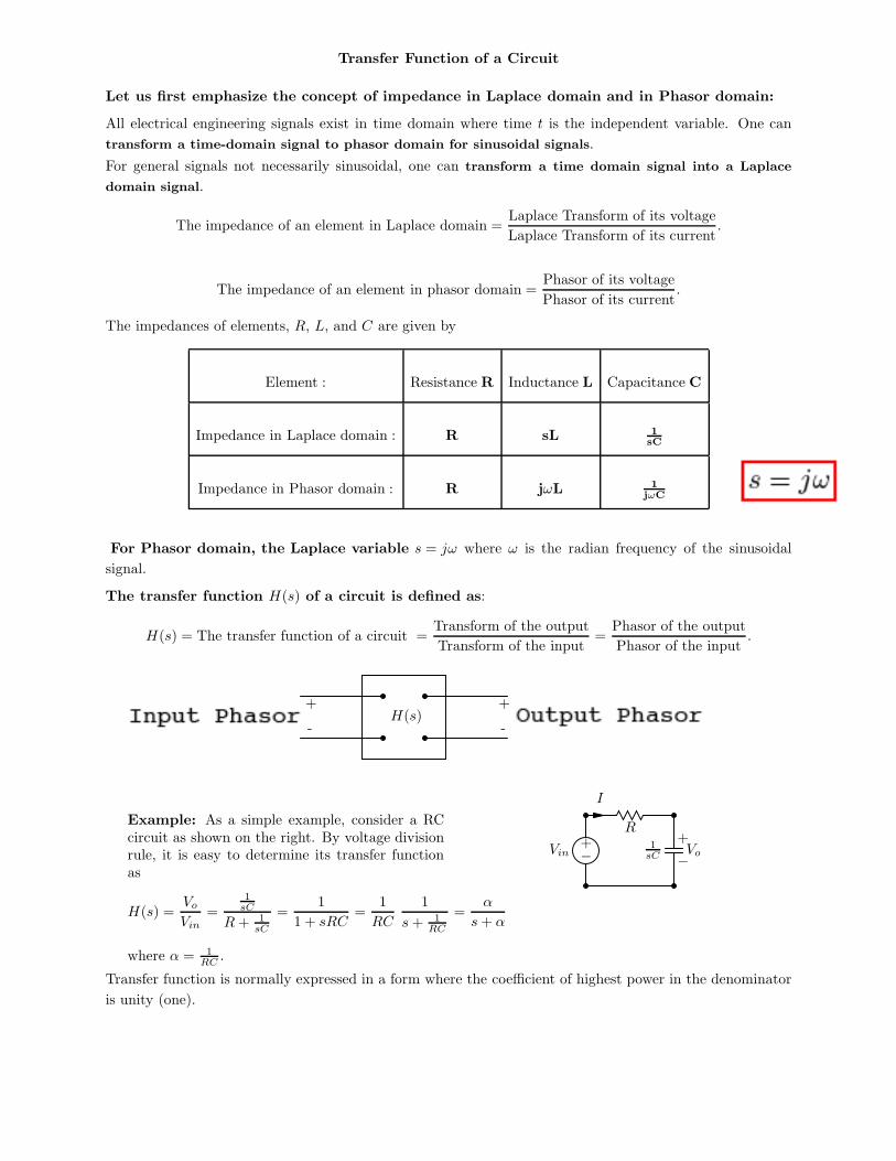
Transfer Function of a Circuit
Let us first emphasize the concept of impedance in Laplace domain and in Phasor domain:
All electrical engineering signals exist in time domain where time t is the independent variable. One can
transform a time-domain signal to phasor domain for sinusoidal signals.
For general signals not necessarily sinusoidal, one can transform a time domain signal into a Laplace
domain signal.
The impedance of an element in Laplace domain =Laplace Transform of its voltage
Laplace Transform of its current.
The impedance of an element in phasor domain =Phasor of its voltage
Phasor of its current.
The impedances of elements, R, L, and C are given by
Element : Resistance R Inductance L Capacitance C
Impedance in Laplace domain : R sL 1sC
Impedance in Phasor domain : R jωL 1jωC
For Phasor domain, the Laplace variable s = jω where ω is the radian frequency of the sinusoidal
signal.
The transfer function H(s) of a circuit is defined as:
H(s) = The transfer function of a circuit =Transform of the output
Transform of the input=
Phasor of the output
Phasor of the input.
+ +
--vin = A cos(ωt) vout = AM(ω) cos(ωt+ θ(ω))H(s)
Example: As a simple example, consider a RCcircuit as shown on the right. By voltage divisionrule, it is easy to determine its transfer functionas
H(s) =Vo
Vin
=1
sC
R+ 1
sC
=1
1 + sRC=
1
RC
1
s+ 1
RC
=α
s+ α
where α = 1
RC.
−+
Vin
I
R
1
sC
+Vo−
Transfer function is normally expressed in a form where the coefficient of highest power in the denominator
is unity (one).
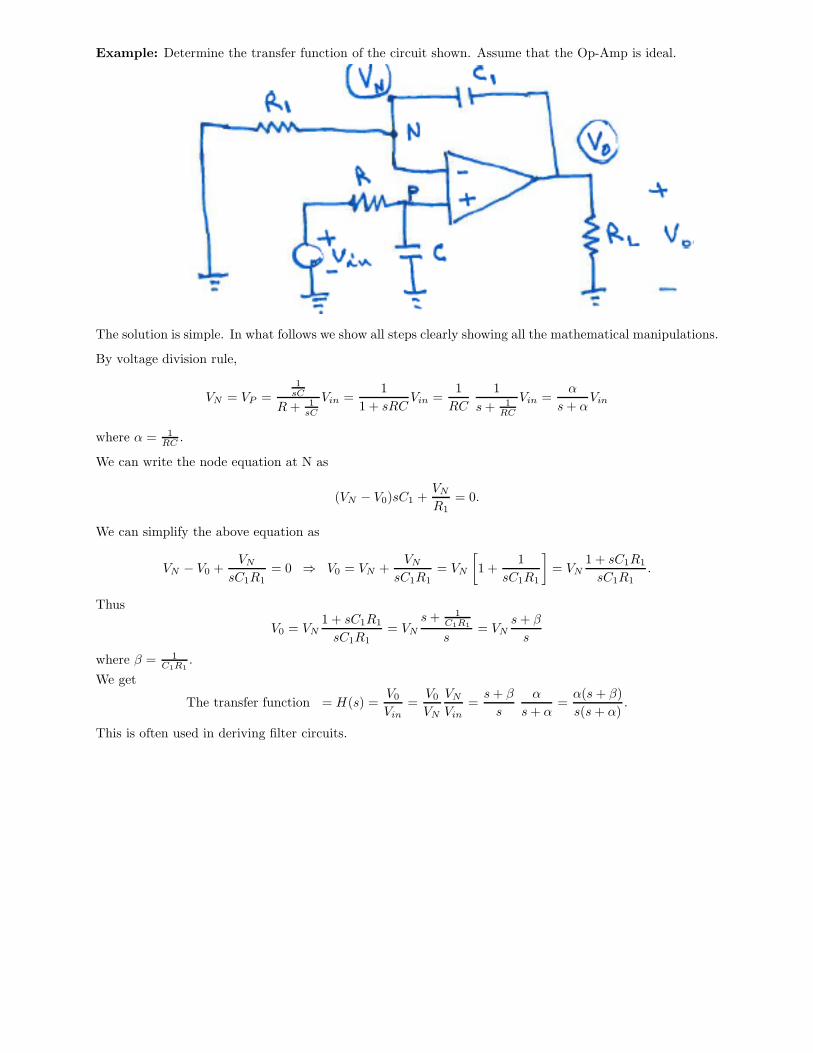
Example: Determine the transfer function of the circuit shown. Assume that the Op-Amp is ideal.
The solution is simple. In what follows we show all steps clearly showing all the mathematical manipulations.
By voltage division rule,
VN = VP =1
sC
R+ 1
sC
Vin =1
1 + sRCVin =
1
RC
1
s+ 1
RC
Vin =α
s+ αVin
where α = 1
RC.
We can write the node equation at N as
(VN − V0)sC1 +VN
R1
= 0.
We can simplify the above equation as
VN − V0 +VN
sC1R1
= 0 ⇒ V0 = VN +VN
sC1R1
= VN
[
1 +1
sC1R1
]
= VN
1 + sC1R1
sC1R1
.
Thus
V0 = VN
1 + sC1R1
sC1R1
= VN
s+ 1
C1R1
s= VN
s+ β
s
where β = 1
C1R1
.
We get
The transfer function = H(s) =V0
Vin
=V0
VN
VN
Vin
=s+ β
s
α
s+ α=
α(s+ β)
s(s+ α).
This is often used in deriving filter circuits.
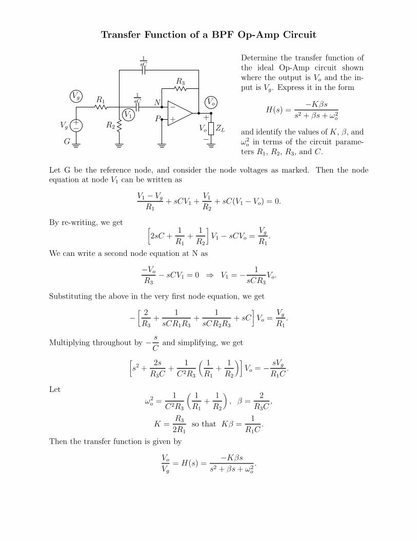
Transfer Function of a BPF Op-Amp Circuit
−+Vg
R1
1
sC−+
R3
ZL
+
Vo
−
N
P
G
R2
1
sC
V1
Vo
Vg
Determine the transfer function ofthe ideal Op-Amp circuit shownwhere the output is Vo and the in-put is Vg. Express it in the form
H(s) =−Kβs
s2 + βs+ ω2o
and identify the values of K, β, andω2
o in terms of the circuit parame-ters R1, R2, R3, and C.
Let G be the reference node, and consider the node voltages as marked. Then the nodeequation at node V1 can be written as
V1 − Vg
R1
+ sCV1 +V1
R2
+ sC(V1 − Vo) = 0.
By re-writing, we get[
2sC +1
R1
+1
R2
]
V1 − sCVo =Vg
R1
.
We can write a second node equation at N as
−Vo
R3
− sCV1 = 0 ⇒ V1 = − 1
sCR3
Vo.
Substituting the above in the very first node equation, we get
−[2
R3
+1
sCR1R3
+1
sCR2R3
+ sC
]
Vo =Vg
R1
.
Multiplying throughout by − s
Cand simplifying, we get
[
s2 +2s
R3C+
1
C2R3
(1
R1
+1
R2
)]
Vo = − sVg
R1C.
Let
ω2
o =1
C2R3
(1
R1
+1
R2
)
, β =2
R3C,
K =R3
2R1
so that Kβ =1
R1C.
Then the transfer function is given by
Vo
Vg
= H(s) =−Kβs
s2 + βs+ ω2o
.
2
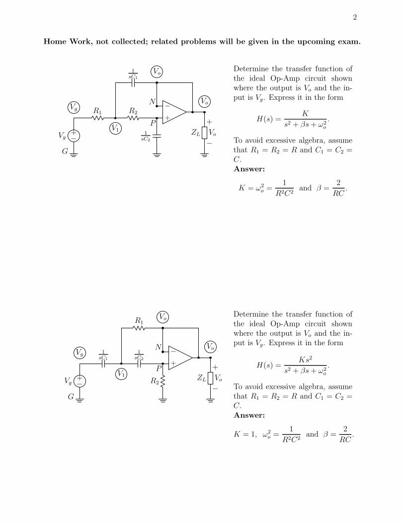
Home Work, not collected; related problems will be given in the upcoming exam.
−+
Vg
R1 R2
−
++
Vo
−ZL
N
P
G
1
sC2
1
sC1
V1
Vo
Vg
VoDetermine the transfer function ofthe ideal Op-Amp circuit shownwhere the output is Vo and the in-put is Vg. Express it in the form
H(s) =K
s2 + βs + ω2o
.
To avoid excessive algebra, assumethat R1 = R2 = R and C1 = C2 =C.Answer:
K = ω2
o=
1
R2C2and β =
2
RC.
−+
Vg
1
sC1
1
sC2
−
++
Vo
−ZL
N
P
G
R2
R1
V1
Vo
Vg
VoDetermine the transfer function ofthe ideal Op-Amp circuit shownwhere the output is Vo and the in-put is Vg. Express it in the form
H(s) =Ks2
s2 + βs + ω2o
.
To avoid excessive algebra, assumethat R1 = R2 = R and C1 = C2 =C.Answer:
K = 1, ω2
o=
1
R2C2and β =
2
RC.

3
−+
Vg
R1 R2
−
++
Vo
−ZL
N
P
G
1
sC2
1
sC1
V1
Vo
Vg
VoDetermine the transfer function ofthe ideal Op-Amp circuit shownwhere the output is Vo and the in-put is Vg. Express it in the form
H(s) =K
s2 + βs + ω2o
and identify the values of K, β, andω2
oin terms of the circuit parame-
ters R1, R2, C1, and C2.
Let G be the reference node, and consider the node voltages as marked. Then the nodeequation at node V1 can be written as
sC1(V1 − Vo) +V1 − Vg
R1
+V1 − Vo
R2
= 0.
We can write a second node equation at P as
Vo − V1
R2
+ sC2Vo = 0.
From the above equation, we get
V1 − Vo = sR2C2 Vo and V1 = (1 + sR2C2)Vo.
Substituting the above in the very first node equation, we get
[
sC1 sR2C2 +1 + sR2C2
R1
+sR2C2
R2
]
Vo =Vg
R1
.
Dividing throughout by C1R2C2 and simplifying, we get
[
s2 +
1
C1
(1
R1
+1
R2
)
s +1
R1R2C1C2
]
Vo =Vg
R1R2C1C2
.
Let
K = ω2
o=
1
R1R2C1C2
and β =1
C1
(1
R1
+1
R2
)
.
Then the transfer function is given by
Vo
Vg
= H(s) =ω2
o
s2 + βs + ω2o
.
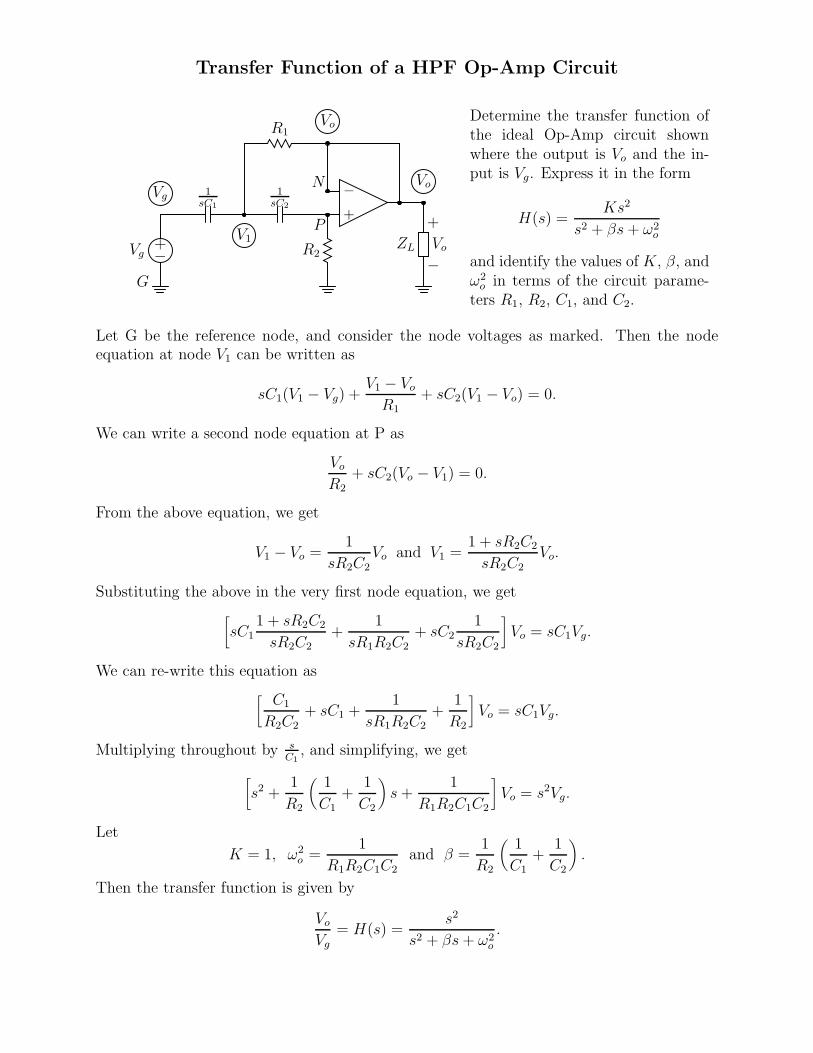
Transfer Function of a HPF Op-Amp Circuit
−+Vg
1
sC1
1
sC2
−+
+
Vo
−ZL
N
P
G
R2
R1
V1
VoVg
VoDetermine the transfer function ofthe ideal Op-Amp circuit shownwhere the output is Vo and the in-put is Vg. Express it in the form
H(s) =Ks2
s2 + βs+ ω2o
and identify the values of K, β, andω2
o in terms of the circuit parame-ters R1, R2, C1, and C2.
Let G be the reference node, and consider the node voltages as marked. Then the nodeequation at node V1 can be written as
sC1(V1 − Vg) +V1 − Vo
R1
+ sC2(V1 − Vo) = 0.
We can write a second node equation at P as
Vo
R2
+ sC2(Vo − V1) = 0.
From the above equation, we get
V1 − Vo =1
sR2C2
Vo and V1 =1 + sR2C2
sR2C2
Vo.
Substituting the above in the very first node equation, we get
[
sC1
1 + sR2C2
sR2C2
+1
sR1R2C2
+ sC2
1
sR2C2
]
Vo = sC1Vg.
We can re-write this equation as
[C1
R2C2
+ sC1 +1
sR1R2C2
+1
R2
]
Vo = sC1Vg.
Multiplying throughout by sC1
, and simplifying, we get
[
s2 +1
R2
(1
C1
+1
C2
)
s+1
R1R2C1C2
]
Vo = s2Vg.
Let
K = 1, ω2
o =1
R1R2C1C2
and β =1
R2
(1
C1
+1
C2
)
.
Then the transfer function is given by
Vo
Vg
= H(s) =s2
s2 + βs+ ω2o
.

HW from Nilsson and Riedel 8th and 9th editions
Some of these problems will appear as quiz or exam problems.
Nilsson and Riedel 8th edition:
9.2, 9.11, 9.12, 9.13, 9.15, 9.23, 9.29, 9.40, 9.48, 9.53, 9.60
Nilsson and Riedel 9th edition:
9.5, 9.11, 9.13, 9.14, 9.16, 9.27, 9.33, 9.45, 9.48, 9.57, 9.63
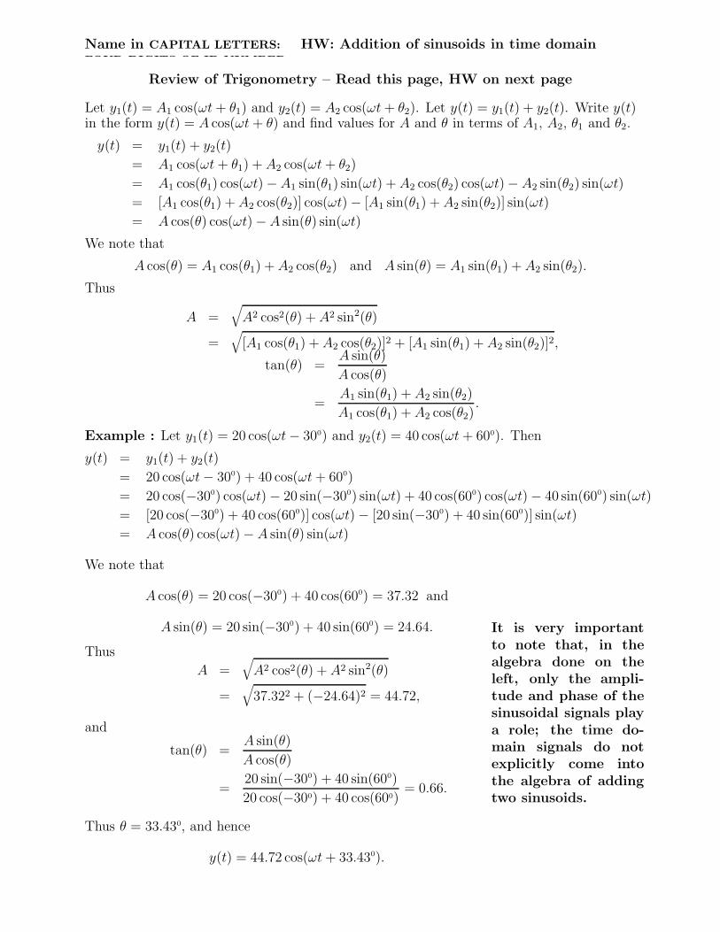
Name in CAPITAL LETTERS: HW: Addition of sinusoids in time domain LAST
FOUR DIGITS OF ID NUMBER:
Review of Trigonometry – Read this page, HW on next page
Let y1(t) = A1 cos(ωt + θ1) and y2(t) = A2 cos(ωt + θ2). Let y(t) = y1(t) + y2(t). Write y(t)in the form y(t) = A cos(ωt + θ) and find values for A and θ in terms of A1, A2, θ1 and θ2.
y(t) = y1(t) + y2(t)
= A1 cos(ωt + θ1) + A2 cos(ωt + θ2)
= A1 cos(θ1) cos(ωt) − A1 sin(θ1) sin(ωt) + A2 cos(θ2) cos(ωt) − A2 sin(θ2) sin(ωt)
= [A1 cos(θ1) + A2 cos(θ2)] cos(ωt) − [A1 sin(θ1) + A2 sin(θ2)] sin(ωt)
= A cos(θ) cos(ωt) − A sin(θ) sin(ωt)
We note that
A cos(θ) = A1 cos(θ1) + A2 cos(θ2) and A sin(θ) = A1 sin(θ1) + A2 sin(θ2).
Thus
A =√
A2 cos2(θ) + A2 sin2(θ)
=√
[A1 cos(θ1) + A2 cos(θ2)]2 + [A1 sin(θ1) + A2 sin(θ2)]2,
tan(θ) =A sin(θ)
A cos(θ)
=A1 sin(θ1) + A2 sin(θ2)
A1 cos(θ1) + A2 cos(θ2).
Example : Let y1(t) = 20 cos(ωt− 300) and y2(t) = 40 cos(ωt + 600). Then
y(t) = y1(t) + y2(t)
= 20 cos(ωt− 300) + 40 cos(ωt + 600)
= 20 cos(−300) cos(ωt) − 20 sin(−300) sin(ωt) + 40 cos(600) cos(ωt) − 40 sin(600) sin(ωt)
= [20 cos(−300) + 40 cos(600)] cos(ωt) − [20 sin(−300) + 40 sin(600)] sin(ωt)
= A cos(θ) cos(ωt) − A sin(θ) sin(ωt)
We note that
A cos(θ) = 20 cos(−300) + 40 cos(600) = 37.32 and
A sin(θ) = 20 sin(−300) + 40 sin(600) = 24.64.
Thus
A =√
A2 cos2(θ) + A2 sin2(θ)
=√
37.322 + (−24.64)2 = 44.72,
and
tan(θ) =A sin(θ)
A cos(θ)
=20 sin(−300) + 40 sin(600)
20 cos(−300) + 40 cos(600)= 0.66.
Thus θ = 33.430, and hence
y(t) = 44.72 cos(ωt + 33.430).
It is very importantto note that, in thealgebra done on theleft, only the ampli-tude and phase of thesinusoidal signals playa role; the time do-main signals do notexplicitly come intothe algebra of addingtwo sinusoids.
2
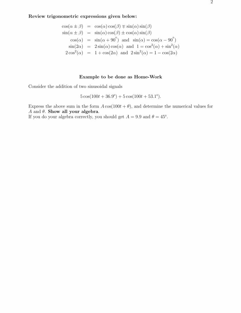
Review trigonometric expressions given below:
cos(α ± β) = cos(α) cos(β) ∓ sin(α) sin(β)
sin(α ± β) = sin(α) cos(β) ± cos(α) sin(β)
cos(α) = sin(α + 900
) and sin(α) = cos(α − 900
)
sin(2α) = 2 sin(α) cos(α) and 1 = cos2(α) + sin2(α)
2 cos2(α) = 1 + cos(2α) and 2 sin2(α) = 1 − cos(2α)
Example to be done as Home-Work
Consider the addition of two sinusoidal signals
5 cos(100t + 36.90) + 5 cos(100t + 53.10).
Express the above sum in the form A cos(100t + θ), and determine the numerical values forA and θ. Show all your algebra.If you do your algebra correctly, you should get A = 9.9 and θ = 450.
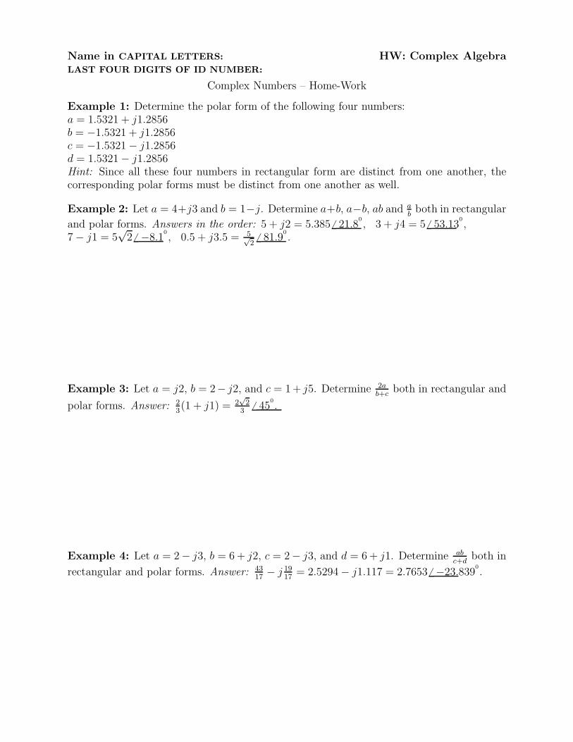
Name in CAPITAL LETTERS: HW: Complex AlgebraLAST FOUR DIGITS OF ID NUMBER:
Complex Numbers – Home-Work
Example 1: Determine the polar form of the following four numbers:a = 1.5321 + j1.2856b = −1.5321 + j1.2856c = −1.5321 − j1.2856d = 1.5321 − j1.2856Hint: Since all these four numbers in rectangular form are distinct from one another, thecorresponding polar forms must be distinct from one another as well.
Example 2: Let a = 4+j3 and b = 1−j. Determine a+b, a−b, ab and a
bboth in rectangular
and polar forms. Answers in the order: 5 + j2 = 5.385 6 21.80
, 3 + j4 = 5 6 53.130
,7 − j1 = 5
√2 6 −8.1
0
, 0.5 + j3.5 = 5√
26 81.9
0
.
Example 3: Let a = j2, b = 2− j2, and c = 1+ j5. Determine 2a
b+cboth in rectangular and
polar forms. Answer: 2
3(1 + j1) = 2
√
2
36 45
0
.
Example 4: Let a = 2− j3, b = 6 + j2, c = 2− j3, and d = 6 + j1. Determine ab
c+dboth in
rectangular and polar forms. Answer: 43
17− j
19
17= 2.5294 − j1.117 = 2.7653 6 −23.839
0
.
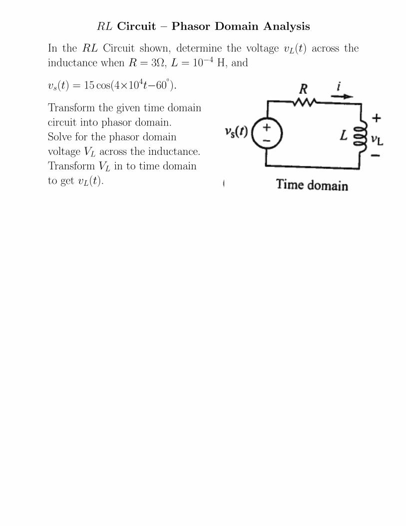
RL Circuit – Phasor Domain Analysis
In the RL Circuit shown, determine the voltage vL(t) across the
inductance when R = 3Ω, L = 10−4 H, and
vs(t) = 15 cos(4×10⁴t−600
).
Transform the given time domain
circuit into phasor domain.
Solve for the phasor domain
voltage VL across the inductance.
Transform VL in to time domain
to get vL(t).
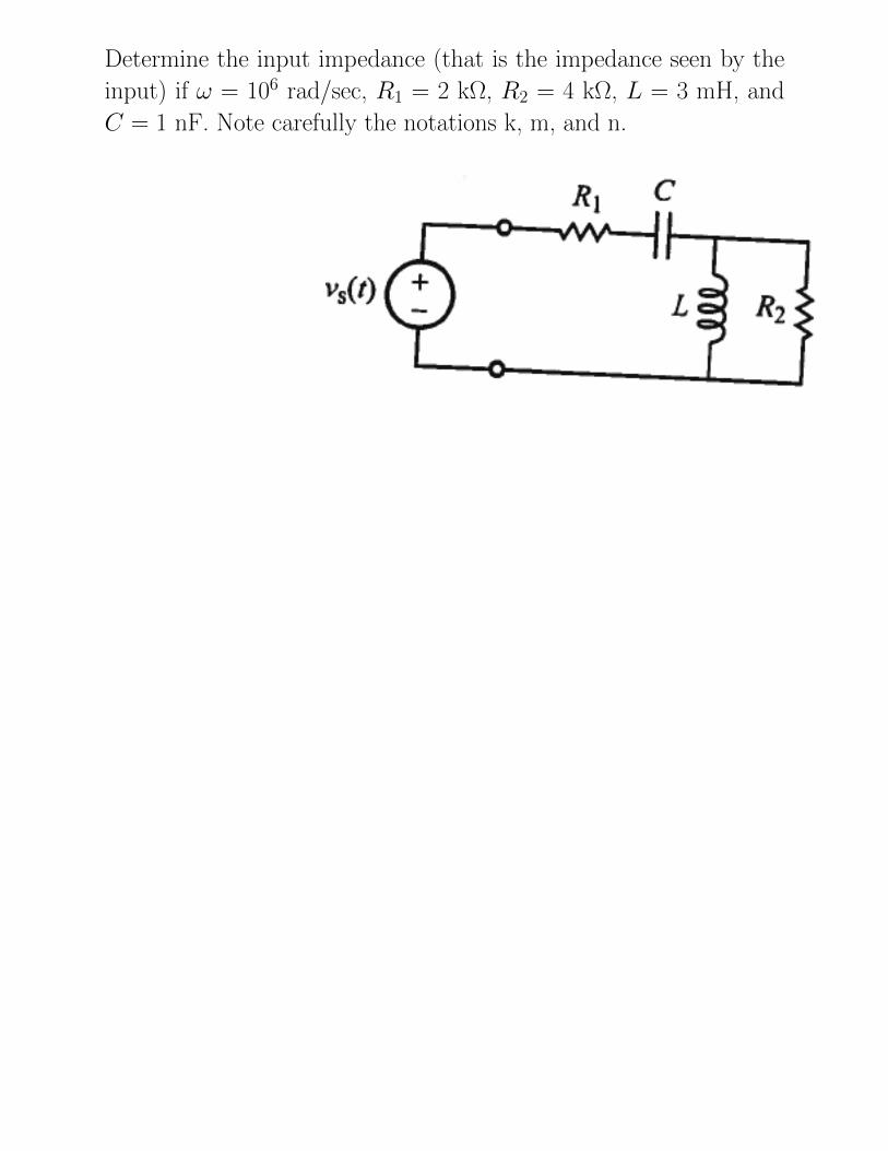
Determine the input impedance (that is the impedance seen by the
input) if ω = 106 rad/sec, R1 = 2 kΩ, R2 = 4 kΩ, L = 3 mH, and
C = 1 nF. Note carefully the notations k, m, and n.
Name in CAPITAL LETTERS: HW: AC Node Voltage MethodLAST FOUR DIGITS OF ID NUMBER:
332:221 Principles of Electrical Engineering I
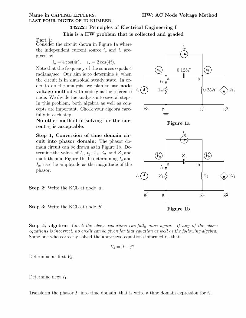
This is a HW problem that is collected and gradedPart 1:Consider the circuit shown in Figure 1a wherethe independent current source ig and is are-given by
ig = 4 cos(4t), is = 2 cos(4t).
Note that the frequency of the sources equals 4radians/sec. Our aim is to determine i1 whenthe circuit is in sinusoidal steady state. In or-der to do the analysis, we plan to use nodevoltage method with node g as the referencenode. We divide the analysis into several steps.In this problem, both algebra as well as con-cepts are important. Check your algebra care-fully in each step.No other method of solving for the cur-rent i1 is acceptable.
is 2i1
ig
1Ω 0.25H
0.125F
i1
g g1 g2g3
a b
va vb
Figure 1a
Step 1, Conversion of time domain cir-cuit into phasor domain: The phasor do-main circuit can be drawn as in Figure 1b. De-termine the values of Is, Ig, Z1, Z2, and Z3 andmark them in Figure 1b. In determining Is andIg, use the amplitude as the magnitude of thephasor.
Is 2I1
Ig
Z1 Z2
Z3
I1
g g1 g2g3
a b
Va Vb
Figure 1b
Step 2: Write the KCL at node ‘a’.
Step 3: Write the KCL at node ‘b’ .
Step 4, algebra: Check the above equations carefully once again. If any of the aboveequations is incorrect, no credit can be given for that equation as well as the following algebra.
Some one who correctly solved the above two equations informed us that
Vb = 9 − j7.
Determine at first Va.
Determine next I1.
Transform the phasor I1 into time domain, that is write a time domain expression for i1.
Name in CAPITAL LETTERS: HW: AC Mesh Current MethodLAST FOUR DIGITS OF ID NUMBER:
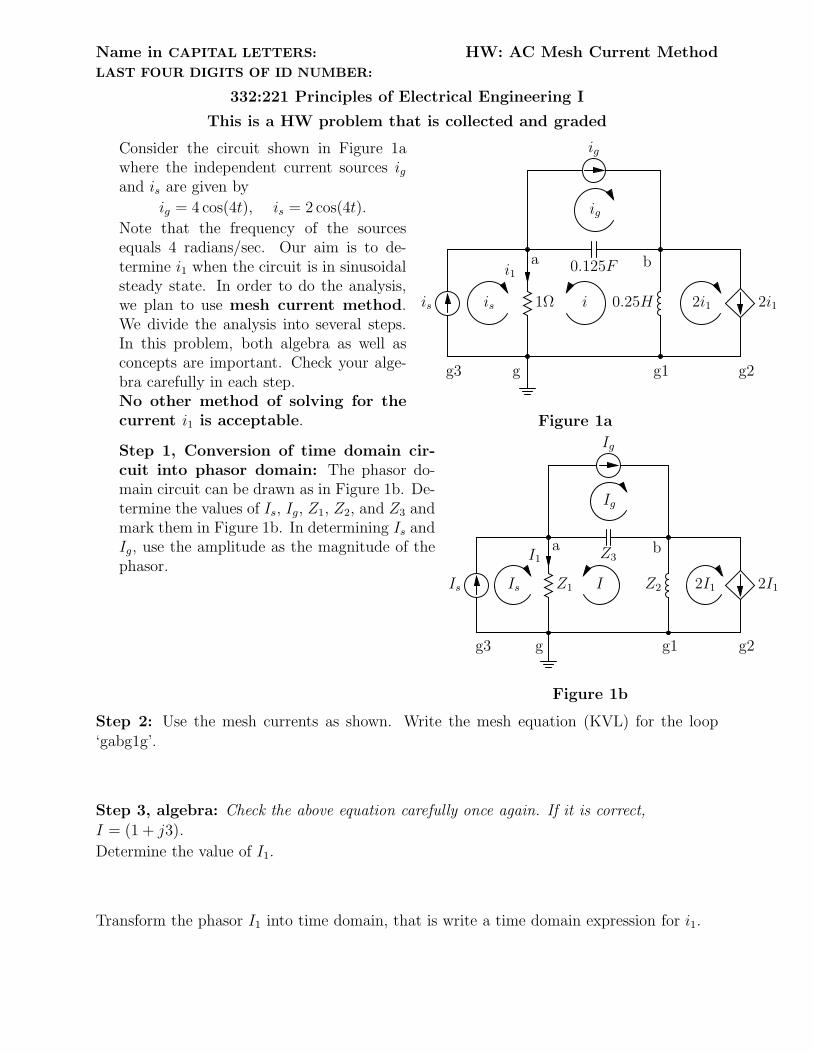
332:221 Principles of Electrical Engineering I
This is a HW problem that is collected and graded
Consider the circuit shown in Figure 1awhere the independent current sources ig
and is are given by
ig = 4 cos(4t), is = 2 cos(4t).
Note that the frequency of the sourcesequals 4 radians/sec. Our aim is to de-termine i1 when the circuit is in sinusoidalsteady state. In order to do the analysis,we plan to use mesh current method.We divide the analysis into several steps.In this problem, both algebra as well asconcepts are important. Check your alge-bra carefully in each step.No other method of solving for thecurrent i1 is acceptable.
is 2i1
ig
1Ω 0.25H
0.125Fi1
g g1 g2g3
a b
is i
ig
2i1
Figure 1a
Step 1, Conversion of time domain cir-cuit into phasor domain: The phasor do-main circuit can be drawn as in Figure 1b. De-termine the values of Is, Ig, Z1, Z2, and Z3 andmark them in Figure 1b. In determining Is andIg, use the amplitude as the magnitude of thephasor.
Is 2I1
Ig
Z1 Z2
Z3I1
g g1 g2g3
a b
Is I
Ig
2I1
Figure 1b
Step 2: Use the mesh currents as shown. Write the mesh equation (KVL) for the loop‘gabg1g’.
Step 3, algebra: Check the above equation carefully once again. If it is correct,
I = (1 + j3).
Determine the value of I1.
Transform the phasor I1 into time domain, that is write a time domain expression for i1.
Name in CAPITAL LETTERS: HW: AC Three Problems
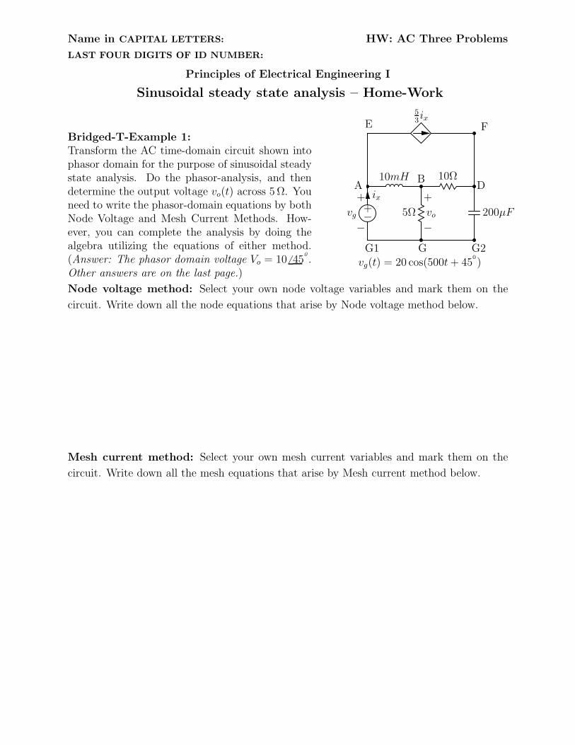
LAST FOUR DIGITS OF ID NUMBER:
Principles of Electrical Engineering I
Sinusoidal steady state analysis – Home-Work
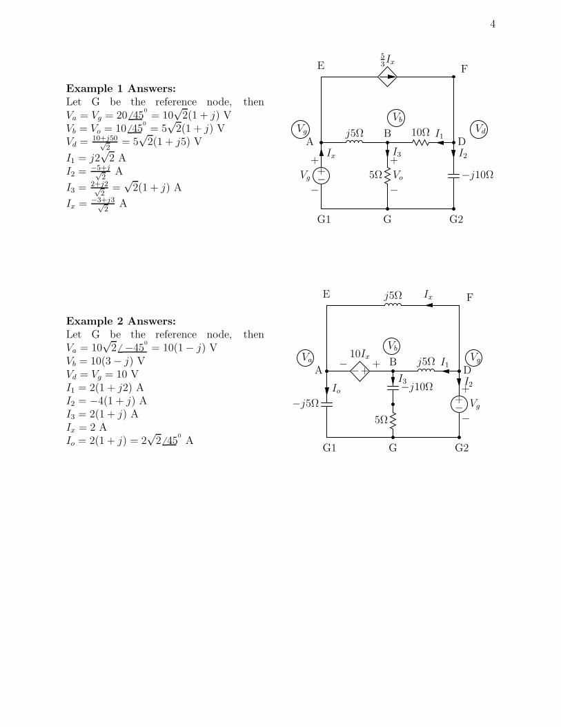
Bridged-T-Example 1:Transform the AC time-domain circuit shown intophasor domain for the purpose of sinusoidal steadystate analysis. Do the phasor-analysis, and thendetermine the output voltage vo(t) across 5 Ω. Youneed to write the phasor-domain equations by bothNode Voltage and Mesh Current Methods. How-ever, you can complete the analysis by doing thealgebra utilizing the equations of either method.(Answer: The phasor domain voltage Vo = 10 6 45
0
.
Other answers are on the last page.)
5
3ix
10Ω
−+
−vg
+A
5Ω
−vo
+
B10mH
200µF
Dix
G1 G2G
E F
vg(t) = 20 cos(500t + 450
)
Node voltage method: Select your own node voltage variables and mark them on the
circuit. Write down all the node equations that arise by Node voltage method below.
Mesh current method: Select your own mesh current variables and mark them on the
circuit. Write down all the mesh equations that arise by Mesh current method below.
2
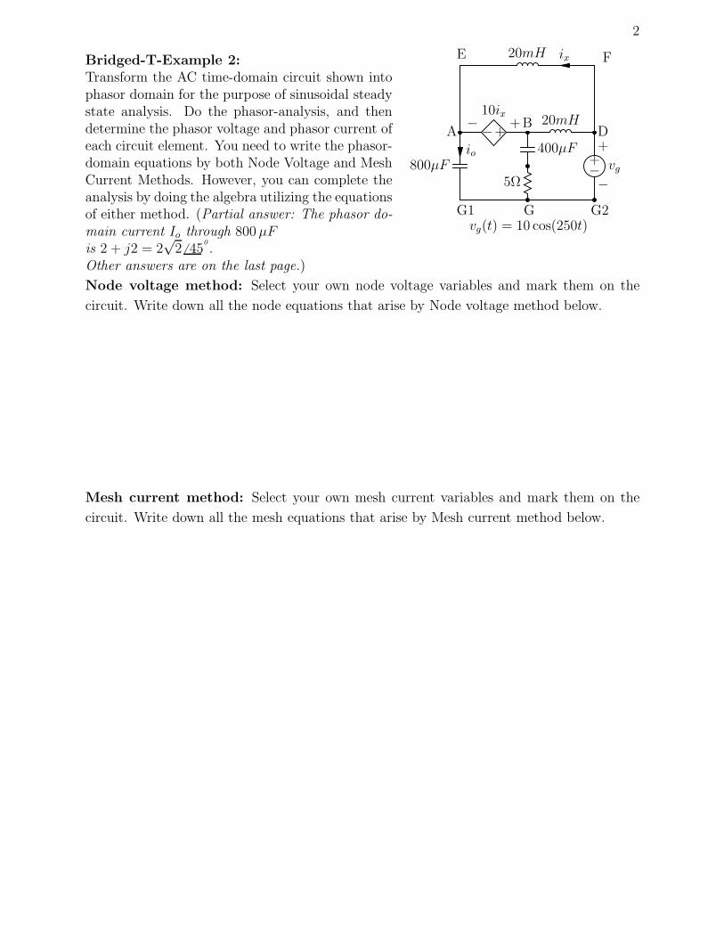
Bridged-T-Example 2:Transform the AC time-domain circuit shown intophasor domain for the purpose of sinusoidal steadystate analysis. Do the phasor-analysis, and thendetermine the phasor voltage and phasor current ofeach circuit element. You need to write the phasor-domain equations by both Node Voltage and MeshCurrent Methods. However, you can complete theanalysis by doing the algebra utilizing the equationsof either method. (Partial answer: The phasor do-
main current Io through 800 µF
is 2 + j2 = 2√
2 6 450
.
Other answers are on the last page.)
−+−
10ix+
20mH
−+
−vg
+D
5Ω
400µF
B 20mH
800µF
A
io
ix
G1 G2G
E F
vg(t) = 10 cos(250t)
Node voltage method: Select your own node voltage variables and mark them on the
circuit. Write down all the node equations that arise by Node voltage method below.
Mesh current method: Select your own mesh current variables and mark them on the
circuit. Write down all the mesh equations that arise by Mesh current method below.

3
Example 3:
Consider the circuit of Example 2, and determine the real and reactive power consumed or
generated by each element by utilizing the voltages and currents obtained in Example 2.
There should be power balance within the expected numerical accuracies.
Use the voltage and current variables given on the next page for Example 2.
4
Example 1 Answers:Let G be the reference node, thenVa = Vg = 20 6 45
0
= 10√
2(1 + j) VVb = Vo = 10 6 45
0
= 5√
2(1 + j) VVd = 10+j50
√
2= 5
√2(1 + j5) V
I1 = j2√
2 AI2 = −5+j
√
2A
I3 = 2+j2√
2=
√2(1 + j) A
Ix = −3+j3√
2A
5
3Ix
10Ω
−+
−Vg
+
A
5Ω
−Vo
+
Bj5Ω
−j10Ω
DIx
G1 G2G
E F
Vg
Vb
Vd
I3 I2
I1
Example 2 Answers:Let G be the reference node, thenVa = 10
√2 6 −45
0
= 10(1 − j) VVb = 10(3 − j) VVd = Vg = 10 VI1 = 2(1 + j2) AI2 = −4(1 + j) AI3 = 2(1 + j) AIx = 2 AIo = 2(1 + j) = 2
√2 6 45
0
A
−+−
10Ix
+
j5Ω
−+
−Vg
+
D
5Ω
−j10Ω
B j5Ω
−j5Ω
A
Io
Ix
G1 G2G
E F
Va
Vb
Vg
I3 I2
I1