SINTERING OF PRINTED NANOPARTICLE STRUCTURES USING … · Laser sintering The laser sintering...
7
SINTERING OF PRINTED NANOPARTICLE STRUCTURES USING LASER TREATMENT N205 Petri Laakso 1 , Saara Ruotsalainen 1 , Eerik Halonen 2 , Matti Mäntysalo 2 , Antti Kemppainen 3 1 VTT Technical Research Centre of Finland, Lappeenranta, 53850, Finland 2 Tampere University of Technology, Institute of Electronics, Tampere, 33101, Finland 3 VTT Technical Research Center of Finland, Oulu, 90571, Finland Abstract Printed intelligence is a promising new technology to produce low-cost electronics. Non-conductive circuits can be printed using nanoscale metal particle inks. Due to the nanoscale size of the particles, the typical sintering temperatures of 100–300 °C are only a fraction of the macroscopic melting point of the corresponding materials, thus allowing the use of paper or plastic substrates. Sintering of printed nanoparticle structures using laser treatment has been investigated at VTT. Laser sintering can be utilized in manufacturing of printed conductor structures such as antennas, circuits and sensors. A drop-on demand printer was used to print patterns with metallo-organic silver nanoparticles on a flexible polyimide substrate. Laser sintering was made with a 940 nm CW fiber coupled diode laser. Process was optimized using different laser power levels, line separation and repetition rounds. Conductivity of laser sintered samples was compared to conductivity of samples sintered in convection oven. Introduction One of the driving forces in printed electronics is the cheap way to produce large amounts of low cost electronics. Then solution is the roll-to-roll production for really high throughput. There are only few potential methods which are truly capable for R2R processing. Laser sintering offers possibility to do R2R sintering. If one wants’ to combine multiple different printed electronic components one needs a way to create contacts between the components. There are several ways to print the contacts but in this paper we chose the ink jet printing of nanoparticles. Metallic nanoparticle inks are used in making of conductors in printed electronics [1]. These inks typically consist of silver or gold nanoparticles (nominal particle diameters 2–50 nm). Particles are encapsulated with a thin protective shell and dispersed in a liquid solvent [2, 3]. After printing a conducting structure can be obtained by sintering, i.e. by partially melting and fusing the adjacent nanoparticles together. Due to the nanoscale size of the particles, the typical sintering temperatures of 100–300 °C are only a fraction of the macroscopic melting point of the corresponding materials [4]. This allows the use of paper or plastic substrates. Recent studies have demonstrated thermally sintered silver and gold conductors with conductivities approaching half of the bulk material conductivity [1, 2, 5]. Since electronics are printed on plastic or fiber based substrates and multiple different materials are used to produce conducting and insulating properties it might not be possible to use oven heating to sinter the nanoparticle ink due other printed materials or substrate may suffer from the heat. Oven sintering is also time consuming. Of course there are also other alternative methods to enable sintering such as electrical sintering [6], UV or microwave [7] illumination. In this research, we have studied laser sintering with diode laser at 940nm. The resistivity of ink-jet- printed tracks on polyimide is demonstrated to be close to bulk silver resistivity, providing same improvement to tracks that were oven-sintered at high temperatures. Benefits for laser sintering are the accurate heat load only where it is needed, the absorbance to the substrate being really low, the short processing time and last but not least it is possible to connect laser to quality monitor to see if the process works like it should. After all laser sintering seems really promising technique. 1360
Transcript of SINTERING OF PRINTED NANOPARTICLE STRUCTURES USING … · Laser sintering The laser sintering...

SINTERING OF PRINTED NANOPARTICLE STRUCTURES USING LASERTREATMENT
N205
Petri Laakso1, Saara Ruotsalainen1, Eerik Halonen2, Matti Mäntysalo2, Antti Kemppainen3
1 VTT Technical Research Centre of Finland, Lappeenranta, 53850, Finland2 Tampere University of Technology, Institute of Electronics, Tampere, 33101, Finland
3 VTT Technical Research Center of Finland, Oulu, 90571, Finland
Abstract
Printed intelligence is a promising new technology toproduce low-cost electronics. Non-conductivecircuits can be printed using nanoscale metal particleinks. Due to the nanoscale size of the particles, thetypical sintering temperatures of 100–300 °C are onlya fraction of the macroscopic melting point of thecorresponding materials, thus allowing the use ofpaper or plastic substrates.
Sintering of printed nanoparticle structures usinglaser treatment has been investigated at VTT. Lasersintering can be utilized in manufacturing of printedconductor structures such as antennas, circuits andsensors. A drop-on demand printer was used to printpatterns with metallo-organic silver nanoparticles ona flexible polyimide substrate. Laser sintering wasmade with a 940 nm CW fiber coupled diode laser.Process was optimized using different laser powerlevels, line separation and repetition rounds.Conductivity of laser sintered samples was comparedto conductivity of samples sintered in convectionoven.
Introduction
One of the driving forces in printed electronics is thecheap way to produce large amounts of low costelectronics. Then solution is the roll-to-rollproduction for really high throughput. There are onlyfew potential methods which are truly capable forR2R processing. Laser sintering offers possibility todo R2R sintering. If one wants’ to combine multipledifferent printed electronic components one needs away to create contacts between the components.There are several ways to print the contacts but inthis paper we chose the ink jet printing ofnanoparticles.
Metallic nanoparticle inks are used in making ofconductors in printed electronics [1]. These inks
typically consist of silver or gold nanoparticles(nominal particle diameters 2–50 nm). Particles areencapsulated with a thin protective shell anddispersed in a liquid solvent [2, 3]. After printing aconducting structure can be obtained by sintering, i.e.by partially melting and fusing the adjacentnanoparticles together. Due to the nanoscale size ofthe particles, the typical sintering temperatures of100–300 °C are only a fraction of the macroscopicmelting point of the corresponding materials [4]. Thisallows the use of paper or plastic substrates. Recentstudies have demonstrated thermally sintered silverand gold conductors with conductivities approachinghalf of the bulk material conductivity [1, 2, 5].
Since electronics are printed on plastic or fiber basedsubstrates and multiple different materials are used toproduce conducting and insulating properties it mightnot be possible to use oven heating to sinter thenanoparticle ink due other printed materials orsubstrate may suffer from the heat. Oven sintering isalso time consuming. Of course there are also otheralternative methods to enable sintering such aselectrical sintering [6], UV or microwave [7]illumination.
In this research, we have studied laser sintering withdiode laser at 940nm. The resistivity of ink-jet-printed tracks on polyimide is demonstrated to beclose to bulk silver resistivity, providing sameimprovement to tracks that were oven-sintered athigh temperatures. Benefits for laser sintering are theaccurate heat load only where it is needed, theabsorbance to the substrate being really low, the shortprocessing time and last but not least it is possible toconnect laser to quality monitor to see if the processworks like it should. After all laser sintering seemsreally promising technique.
1360

Experimental
Printing of sintered conductors
The samples for the laser sintering trials were inkjetprinted in Tampere University of Technology. Theused printer was iTi XY2.0 Material DepositionSystem, in figure 1 below. The printer has arepeatability of ± 1 µm and the maximum substratesize is 305 mm x 305 mm. Generally the printingspeed is somewhere around 100-200 mm/s. The printhead was Spectra SQ-128 (Figure 2), which createsdrops of 10 pl. There are 128 nozzles in the head andthe nozzle spacing is 508 microns and the diameter ofa nozzle 35 µm.
Fig. 1: iTi XY2.0 material deposition system
Fig. 2: Spectra print head
The chosen substrate was Kapton® (Polyimide).There was not made other surface treatments to thesubstrate than cleaning with isopropanol before
printing. The pattern that was printed consist severalponsa (shown in figure 3) structures. In all structuresthe constant A was 15 mm and the constant B was100 µm, 200 µm, or 350 µm. The one layer patternswere printed at the resolution of 600 dpi. Thetemperature of the printing plate of the printer was60 ºC. So the ink dried a bit but did not sinter.
B
A
Fig. 3: Test geometry.
The first used silver nanoparticle ink in printing wasInk 1 whose curing conditions in convection oven are100-350 °C for 1-60 minutes. However there weresome problems with the jetting of the ink and hencethe imprint was not as good as desired. Some resultswere got but many of the lines were broken. Brokenwires were neglected in sintering.The second set of trials was made with Ink 2 that wasalso a silver nanoparticle ink. Metal content wasabout two times higher than in Ink 1 and therefore itoffers better conductivity. The advantage of it wasalso that it is jetting better with our print heads.Normal sintering conditions of the ink are 210-220 °C for 60 minutes. The imprint was better withthis ink and the results were also easier to get.
Laser sintering
The laser sintering experiments were performed atVTT in Lappeenranta. The laser system (fig. 4) usedin the experiments was a Laserline LDF400-200 fibercoupled diode laser, where the laser beam was guidedvia an Ø400 µm optical fiber to a scanhead. Thediode laser is operated at 940 ± 10 nm wavelengthand the focal length used was 163 mm resulting anØ1.0 mm focal spot on the work piece. The beamprofile used was top hat beam. Sintering tests weredone at the focal point and in some tests the beamwas defocused -32 mm to achieve ca. Ø6 mm spot towork piece. Beam profiles in the focal spot anddefocused beam profile are presented in the figure 5.In the sintering tests the film was placed on the top oftwo glass plates so that the pattern to be sintered washanging on free space. Samples were sintered fromthe printed side of the film.
1361

Fig. 4: Laser sintering setup.
Fig. 5: Beam profiles a) focal spot (beam Ø 1 mm) b)defocused -32 mm (beam Ø 6 mm).
Samples were sintered by scanning multiple verticallines across the ponsa pattern, line spacing was0.2mm (figure 6). Tests were done in focal plane andalso in defocus.
20 mm
5 m
m
0,2 mm
Fig. 6: Sintering path when laser beam was used inthe focal spot.
Sintering experiments were performed using differentlaser powers and number of sintering times to foundout the optimal sintering parameters. In all tests thescanning speed was 1000 mm/s. When the focusedlaser beam was used laser powers were between 20and 50 W. When defocused laser beam was usedlaser powers were between 30 and 197 W. Some testswere done also by sintering samples 1, 2, 5 and 10times. In these tests used laser powers were 50 or 80W. These tests were done in defocus.
Laser Sintering Process
When thinking about the laser sintering process onewould need a smooth heat input with minimumamount of differences and small absorbance to thebase material. Laser has this advantage to bring verylocalized heat input [8, 9, 10, 11, 12]. Smooth inputcomes from the beam spatial profile and top hat modethen would be preferred. Diode lasers offer normallythis top hat mode and the chosen 940nm does nothave too high absorbance to the used PI substrate.Also pulsing of the laser is not preferred and that iswhy continuous wave laser is good alternative.
If high average powers are used the intensity mightget quite high. This can be adjusted so that the beamsize is the same as the width of the conductor andthen sintering can be made only with one pass. If it isnot possible to bring enough energy to the materialwith one pass, it is possible to heat up materialgradually with several passes. For example if inkcontains too much solvent and the vaporization ofsolvent interferes with the sintering process, thenmultiple passes is the right approach. Anothermethod is to use line wise method so that beam isscanned back and forth over the whole area to besintered. This way the sintering has to be even fasterdue the sintering has to happen within less than 1 msat a time and the process window is a lot smaller duereally fast process. In this line wise method sinteredlines can be overlapped so that conductors are heatedgradually and also cooled gradually. Laser movingspeed has to be some meters per second and thenmaterial does not have time to cool down too muchbetween passes. Still it is common for all strategies toheat up the material quickly and locally to enable thesintering, low process times and minimal heat effectto the substrate.
Results and Discussion
In sintering tests two different inks were tested andtest geometry was like what is shown in Figure 3.Three different line thicknesses were printed to seewhat the effect of line width is.
First sintering tests were made with Ink 1 printedgeometries using hatch technique. Laser speed was1000 mm/s and line to line distance 0.2 mm. Beamsize was 1 mm in diameter. After series of pre tests itwas found out that the optimal range could bebetween 20 – 50 W average powers. From table 1.one can see the effect of average power to sheetresistance.
1362

Table 1 Sheet resistance values with different averagepowers.
50 W 40 W 30 W 20 W
100 µm 0,16 0,18 0,29 0,52
200 µm 0,17 0,27 0,31 0,59
350 µm 0,16 0,19 0,28 0,38
From these results can be seen that the higher theaverage power was the lower the resistance was. Ifhigher than 50 W average power was used,nanoparticle ink starts really easily to burn andconductivity is not as good anymore. Bulk resistanceof silver is 1.6 µOhm·cm. If accurate layer thicknessof tested samples would be known, the bulkresistance of the sintered samples could becalculated. Layer thickness is around 1-2 µm whichwould mean almost the same bulk resistance as withthe bulk silver.
Laser sintering is quite sensitive if any dust particlesetc. are on the substrate during sintering. Theseimpurities would absorb laser light more than the inkand this is why a serious damage may occur to thesurface of ink or substrate.
After laser sintering and measuring of samples theywhere put to convection oven to sinter the materialsthoroughly. Small increase in conduction was noticedbut this still needs further testing to get reliable data.Anyway this indicates that laser sintering did notsinter the nanoparticle ink fully. When ink 1 was onlyoven sintered 60 minutes at 160°C, the average sheetresistance of 12 samples after sintering was 0.46ohm. This is a bit worse than what was obtained withlaser but due PET substrate oven temperature was notas high as would be needed to sinter ink fully. Thisvalue for oven sintering is also only couple timeshigher value than with bulk silver which is goodresult.
Due nanoparticle ink 1 was not so easy to print it wasdecided to change the ink to Ink 2 to get better printquality. With the new ink it was immediately noticedthat this ink does not allow as high laser intensity asthe ink 1. In figure 7 we can see the damage tosintered Ink 2 due too high intensity.
Fig. 7: Ink 2 sintered with 40W in focus with hatchmethod.
Because as high intensities could not be used as withInk 1, the laser beam was decided to be enlarged tomake intensity lower and to give process more time.Sintering seemed to work better even if sintering wasdone multiple times. Again after short pre tests it wasfound out that right parameter window was between80 and 197 W with the 6 mm beam used. From table2 one can see how conductivity changes whenaverage power is changed. Less than 80 W averagepower sintering does not seem to work.
Table. 2 Different average powers and correspondingsheet resistance values of 100 µm wide sintered
lines.Average power
[W]Resistance
[Ohm]
197 14,3
180 16,8
160 17,1
140 20,3
120 25,3
100 24,9
90 33,5
80 148
70 N/A
With multiple scanning technique was tried to see ifquasi-simultaneous sintering could be done. FromFigure 8 we can see that laser powers below sinteringthreshold with one pass does sinter the material by
1363

multiple passes. This makes process also more gentlefor the ink. Of course this kind of operation takesmore time but also it would enable more solventcontaining inks to be sintered. It is notable that if inkis already once sintered it does not sinter more withmultiple passes with the same laser power and speed.This might be also due after first sintering the surfaceof line changes color to human eye from light blue tosilver like outlook. This silver surface will mostprobably reflect near infrared light really well whichin fact lets lower amount of light to the process itselfand may explain why multiple passes does not help iffirst pass sinters the conductor. Well a way aroundthis might be the increase in power in consecutivepasses but this may lead to substrate damage and thatis why it was not tested. With ten passes and highaverage power material may suffer due high heatinput (see figure 8 lowest right and the red arrow).
Fig. 8: Multiple pass tests with consecutive sheetresistance.
When ink 2 was only oven sintered 60 minutes at260°C the average sheet resistance of 12 samplesafter sintering was 0.05 ohm. This is again a bit betterthan what was obtained with laser. Againmeasurement was done in different place soconfirmation is needed. This value also is really closeto bulk silver value.
One issue in both tested inks was that solvent fromthe ink evaporates when sintering. It can be seen afterprocess with microscope that evaporated ink spreadson both sides of the conductor which might causeproblems in the next steps of whole productionprocess. In figure 7 one can also see this evaporatedresidue near the sintered conductor.
Another issue seen as a problem in laser sintering isthe thickness variation of printed ink. In figure 9 wecan see a picture about differences in printing qualityand thickness before laser sintering. At some pointsthickness of the printed ink is so thin that one caneven see through.
Fig. 9: After printing, thickness differences of ink.
If one can see through the printed layer it is clear thatthe absorbance of laser light into this printed area hasto be different than places where thickness is so thickthat one cannot see through the printed conductor. Infigure 10 we can see the thickness variation aftersintering. Picture is not exactly at the same positionthan in figure 9 but thickness variation is similar. It isobvious that ink is only partially sintered. Sinteredmaterial have silver outlook and blue parts areunsintered. It is certain that laser has passes all areasdue multiple similar tests made.
50 W x1 N/A
50 W x5 ~ 0,42
50 W x10 ~ 0,34
80 W x1 ~ 0,11
80 W x5 ~ 0,08
80 W x10 ~ 0,11
1364
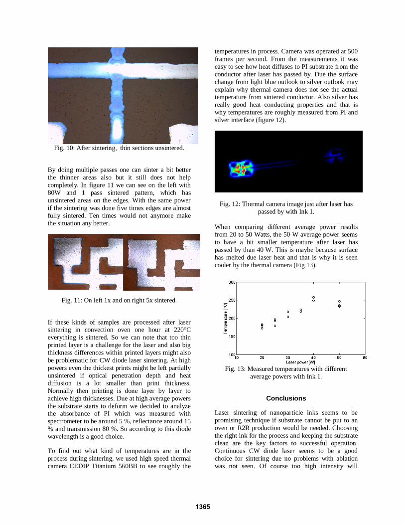
Fig. 10: After sintering, thin sections unsintered.
By doing multiple passes one can sinter a bit betterthe thinner areas also but it still does not helpcompletely. In figure 11 we can see on the left with80W and 1 pass sintered pattern, which hasunsintered areas on the edges. With the same powerif the sintering was done five times edges are almostfully sintered. Ten times would not anymore makethe situation any better.
Fig. 11: On left 1x and on right 5x sintered.
If these kinds of samples are processed after lasersintering in convection oven one hour at 220°Ceverything is sintered. So we can note that too thinprinted layer is a challenge for the laser and also bigthickness differences within printed layers might alsobe problematic for CW diode laser sintering. At highpowers even the thickest prints might be left partiallyunsintered if optical penetration depth and heatdiffusion is a lot smaller than print thickness.Normally then printing is done layer by layer toachieve high thicknesses. Due at high average powersthe substrate starts to deform we decided to analyzethe absorbance of PI which was measured withspectrometer to be around 5 %, reflectance around 15% and transmission 80 %. So according to this diodewavelength is a good choice.
To find out what kind of temperatures are in theprocess during sintering, we used high speed thermalcamera CEDIP Titanium 560BB to see roughly the
temperatures in process. Camera was operated at 500frames per second. From the measurements it waseasy to see how heat diffuses to PI substrate from theconductor after laser has passed by. Due the surfacechange from light blue outlook to silver outlook mayexplain why thermal camera does not see the actualtemperature from sintered conductor. Also silver hasreally good heat conducting properties and that iswhy temperatures are roughly measured from PI andsilver interface (figure 12).
Fig. 12: Thermal camera image just after laser haspassed by with Ink 1.
When comparing different average power resultsfrom 20 to 50 Watts, the 50 W average power seemsto have a bit smaller temperature after laser haspassed by than 40 W. This is maybe because surfacehas melted due laser heat and that is why it is seencooler by the thermal camera (Fig 13).
Fig. 13: Measured temperatures with differentaverage powers with Ink 1.
Conclusions
Laser sintering of nanoparticle inks seems to bepromising technique if substrate cannot be put to anoven or R2R production would be needed. Choosingthe right ink for the process and keeping the substrateclean are the key factors to successful operation.Continuous CW diode laser seems to be a goodchoice for sintering due no problems with ablationwas not seen. Of course too high intensity will
1365

vaporize the ink. Since samples were a bit pre driednext step might be sintering of these conductors rightafter printing when they contain much more solvent.This high amount of solvent might be a problem ifthe same laser parameters would be tested.
Laser sintering seems to be really sensitive if printedlayer is too thin or there is too much variation inthickness. Resistance values are already quite close towhat bulk silver has so this is good thing, but stillprocess has to be improved and testing is to be donealso in real Roll to Roll environment in the nearfuture.
References
[1] Redinger D, Molesa S, Yin S, Farschi R andSubramanian V 2004 IEEE Trans. Electron Devices51 1978–83
[2] Kim D and Moon J 2005 Electrochem. Solid-State Lett.8 J30–3
[3] Lee H-H, Chou K-S and Huang K-C 2005Nanotechnology 16 2436–41
[4] Buffat P and Borel J-P 1976 Phys. Rev. A 132287–98
[5] Fuller S B, Wilhelm E J and Jacobson J M 2002 J.Microelectromech. Syst. 11 54–60
[6] Allen, M.; Aronniemi, M.; Mattila, T.; Alastalo,A.; Ojanperä, K.; Suhonen, M.; Seppä, H.: Electricalsintering of nanoparticle structures. In:Nanotechnology 19 (2008) 175201
[7] Perelaer J, deGans B-J and Schubert U S 2006Adv. Mater. 18 2101–4
[6] Bieri N R, Chung J, Haferl S E, Poulikakos D andGrigoropoulos C P 2003 Appl. Phys. Lett. 82 3529–31
[7] Chung J, Ko S, Bieri N R, Grigoropoulos C P andPoulikakos D 2004 Appl. Phys. Lett. 84 801–3
[8] Khan, A.; Rasmussen, N.; Marinov.; Svenson, O.:Laser Sintering of Nanomaterial on PolymerSubstrates. In: journal of Microelectronics andelectronic Packaging (2008)5, 77-86
[9] Khan, A.; Rasmussen, N.; Marinov.; Svenson, O.:Laser Sintering of Direct Write silver nano-inkconductors for microelectronic applications. In:Photon Processing in Microelectronics and PhotonicsVII, edited by Andrew, S. et al. Proc of SPIE Vol.6879, 687910, (2008).
[10] Ko S.; Pan H.; Grigoropoulos C.; Luscombe C.;Frechet J.; Poulikakos D.: All-inkjet-printed flexibleelectronics fabrication on a polymer substrate by low-temperature high-resolution selective laser sinteringof metal nanoparticles, Nanotechnology 18 (2007)345202.
[11] Ko S.; Pan H.; Grigoropoulos C.; Luscombe C.;Frechet J.; Poulikakos D.: Air stable high resolutionorganic transistors by selective laser sintering of ink-jet printed metal nanoparticles, Applied PhysicsLetters 90, 141103, 2007.
[12] Auyeung, R.; Kim H, Mathews, S.; Piqué, A.:Laser Direct-Write of Metallic Nanoparticle Inks,JLMN-Journal of Laser Micro/Nanoengineering Vol.2, No. 1, 2007.
Meet the Author
Petri Laakso works as research scientist at VTT andhas worked with several different fields of lasermaterials processing such as cutting, welding ofpolymers, laser ablation with ultra fast lasers andsystems integration.
1366