SINTEF Wafers We studied two wafers. Wafer #24 and one oxygenated wafer.
13
SINTEF Wafers • We studied two wafers. Wafer #24 and one oxygenated wafer.
-
date post
21-Dec-2015 -
Category
Documents
-
view
236 -
download
2
Transcript of SINTEF Wafers We studied two wafers. Wafer #24 and one oxygenated wafer.

SINTEF Wafers
• We studied two wafers. Wafer #24 and one oxygenated wafer.

PSIDevices Purdue Devices
Diode cluster
JHU Devices JHU Devices
BTev Devices
N+ side
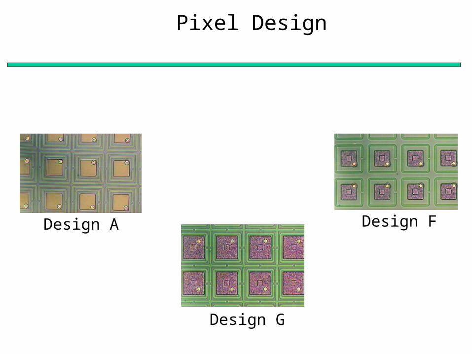
Design A Design F
Design G
Pixel Design
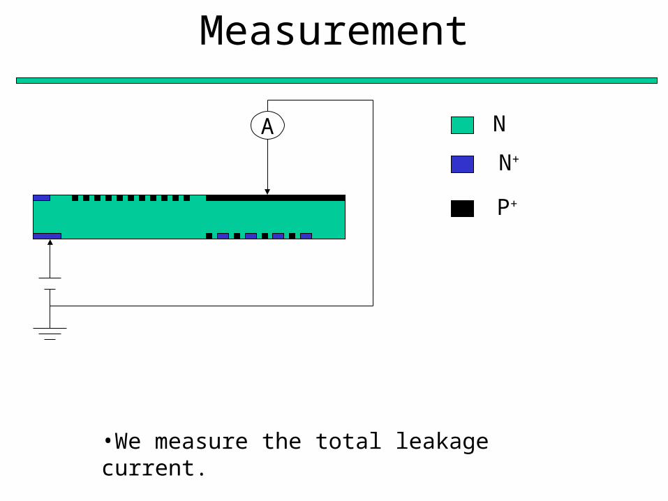
Measurement
A
•We measure the total leakage current.
N
N+
P+

Wafer #24
• IV measurement on wafer 24 is complete. We are now going to wire bond it to study single pixel characteristics.

Summary

• Except Pixel 1, AI has high breakdown.

•Pixel 4 - design F , Pixel 5 - design G•Design F and G also have high breakdown voltage.

•Vbreakdown < 300 - 7 pixel arrays.• 300 < Vbreakdown < 500 - 20 pixel arrays•500 < Vbreakdown - 7 pixel arrays
•Current per unit area at 270 V - 3-6 nA/cm^2
Performance

SINTEF Oxygenated Wafer
• We measured 15 pixel arrays, Purdue and PSI designs, on the oxygenated wafer.

•Breakdown voltage is low
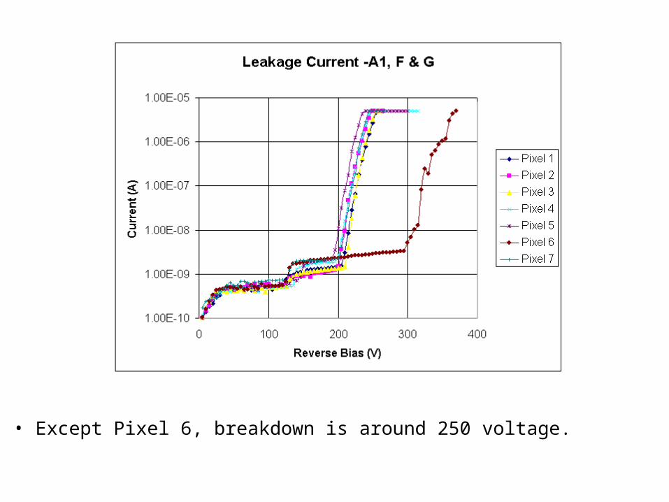
• Except Pixel 6, breakdown is around 250 voltage.

•Vbreakdown < 200 - 4 pixel arrays.• 200 < Vbreakdown < 250 - 10 pixel arrays•250 < Vbreakdown - 1 pixel array
•Current per unit area at 270 V - 11 nA/cm^2(Data for pixel 6 only. For all other pixel arraysVbreakdown < 250)
Performance