Single wall carbon nanotube/titania nanocomposite ... Shoubra/Engineering...Single wall carbon...
7
Single wall carbon nanotube/titania nanocomposite photoanodes enhance the photovoltaic performance of cadmium selenide quantum dot-sensitized solar cells Ali Badawi a,n , N. Al-Hosiny a,b , S. Abdallah a,c , Amar Merazga a , H. Talaat d a Department of Physics, Faculty of Science, Taif University, Taif, Saudi Arabia b Department of Physics, Faculty of Science, Aljouf University, Saudi Arabia c Department of Mathematical and Physical Engineering, Faculty of Engineering (Shoubra), Benha University, Cairo, Egypt d Physics Department, Faculty of Science, Ain Shams University, Abbassia Cairo, Egypt article info Available online 13 May 2014 Keywords: SWCNTs/TiO 2 nanocomposite photoanode CdSe quantum dot Direct adsorption Quantum dots sensitized solar cell Photovoltaic cells abstract Improving the photovoltaic performance of CdSe quantum dots sensitized solar cells (QDSSCs) using 0.2 wt% of single walled carbon nanotubes/Titania (SWCNTs/TiO 2 ) nano- composite photoanode is reported. These SWCNTs/TiO 2 nanocomposite films were prepared by mechanical mixing and spread on the photoanode by a doctor blade method. The current density–voltage (J–V) characteristic curves of such assembled QDSSCs were measured at AM 1.5 simulated sunlight. Solar cells based on SWCNTs/TiO 2 nanocomposite photoanode achieves 58% increase in power conversion efficiency (η) compared with those based on plain TiO 2 NPs photoanode under a AM 1.5 simulated sunlight and for dipping time of 6 h. The significant improvement of J sc and η for CdSe QDSSCs based on SWCNTs/TiO 2 nanocomposite photoanode is due to the enhancement in the absorption of the incident light and rapid electron transport through the SWCNTs compared to the plain TiO 2 NPs. Furthermore, the linear increase in J sc with increasing intensity of the sunlight indicates the sensitivity of the assembled cells. & 2014 Elsevier Ltd. All rights reserved. 1. Introduction Throughout the last decade, science has made great strides towards improving the performance of quantum dots sensi- tized solar cells (QDSSCs) [1–5]. In this type of solar cell, quantum dots (QDs) are adsorbed onto large band gap metal oxides nanoparticles (NPs) such as TiO 2 [6, 7], ZnO [7, 8], or SnO 2 [7] to act as sensitizers. Among the parameters that make QDs attractive candidates are the ability of tuning the band gap of these QDs through size control to match the sunlight spectra [2, 9, 10], high extinction coefficients due to quantum confinement effects [6, 11], unique electronic and optical properties, large intrinsic dipole moments that lead to rapid charge separation [12], and intrinsically strong light absorbers [13]. Furthermore, QDSSCs have larger surface areas and provide a technically and economically credible alterna- tive to conventional cells, such as silicon photovoltaic or dye- sensitized solar cells (DSSCs). DSSCs have many limitations, such as difficulties in utilizing the infrared region of the solar spectrum and instability over long periods of time. Several research efforts have already been carried out using the following QDs as photosensitizers: CdS [14, 15], CdSe [10, 16– 18], CdTe [2, 19], PbSe [20], PbS [21, 22], InAs [23], ZnSe [24], and Ag 2 Se [25]. Cadmium chalcogenides (CdX; X¼ S, Se, and Te) QDs are relatively simple to synthesize, and easy to control their sizes to harvest as much light energy, especially in the visible region of the solar spectrum. These characteristics make CdX QDs appropriate sensitizers for making QDSSCs Contents lists available at ScienceDirect journal homepage: www.elsevier.com/locate/mssp Materials Science in Semiconductor Processing http://dx.doi.org/10.1016/j.mssp.2014.04.028 1369-8001/& 2014 Elsevier Ltd. All rights reserved. n Corresponding author. Tel.: þ966 543414808; fax: þ966 27241880. E-mail address: [email protected] (A. Badawi). Materials Science in Semiconductor Processing 26 (2014) 162–168
Transcript of Single wall carbon nanotube/titania nanocomposite ... Shoubra/Engineering...Single wall carbon...

Contents lists available at ScienceDirect
Materials Science in Semiconductor Processing
Materials Science in Semiconductor Processing 26 (2014) 162–168
http://d1369-80
n CorrE-m
journal homepage: www.elsevier.com/locate/mssp
Single wall carbon nanotube/titania nanocompositephotoanodes enhance the photovoltaic performanceof cadmium selenide quantum dot-sensitized solar cells
Ali Badawi a,n, N. Al-Hosiny a,b, S. Abdallah a,c, Amar Merazga a, H. Talaat d
a Department of Physics, Faculty of Science, Taif University, Taif, Saudi Arabiab Department of Physics, Faculty of Science, Aljouf University, Saudi Arabiac Department of Mathematical and Physical Engineering, Faculty of Engineering (Shoubra), Benha University, Cairo, Egyptd Physics Department, Faculty of Science, Ain Shams University, Abbassia Cairo, Egypt
a r t i c l e i n f o
Available online 13 May 2014
Keywords:SWCNTs/TiO2 nanocomposite photoanodeCdSe quantum dotDirect adsorptionQuantum dots sensitized solar cellPhotovoltaic cells
x.doi.org/10.1016/j.mssp.2014.04.02801/& 2014 Elsevier Ltd. All rights reserved.
esponding author. Tel.: þ966 543414808; faail address: [email protected] (A. Bad
a b s t r a c t
Improving the photovoltaic performance of CdSe quantum dots sensitized solar cells(QDSSCs) using 0.2 wt% of single walled carbon nanotubes/Titania (SWCNTs/TiO2) nano-composite photoanode is reported. These SWCNTs/TiO2 nanocomposite films wereprepared by mechanical mixing and spread on the photoanode by a doctor blade method.The current density–voltage (J–V) characteristic curves of such assembled QDSSCs weremeasured at AM 1.5 simulated sunlight. Solar cells based on SWCNTs/TiO2 nanocompositephotoanode achieves 58% increase in power conversion efficiency (η) compared withthose based on plain TiO2 NPs photoanode under a AM 1.5 simulated sunlight and fordipping time of 6 h. The significant improvement of Jsc and η for CdSe QDSSCs based onSWCNTs/TiO2 nanocomposite photoanode is due to the enhancement in the absorption ofthe incident light and rapid electron transport through the SWCNTs compared to the plainTiO2 NPs. Furthermore, the linear increase in Jsc with increasing intensity of the sunlightindicates the sensitivity of the assembled cells.
& 2014 Elsevier Ltd. All rights reserved.
1. Introduction
Throughout the last decade, science has made great stridestowards improving the performance of quantum dots sensi-tized solar cells (QDSSCs) [1–5]. In this type of solar cell,quantum dots (QDs) are adsorbed onto large band gap metaloxides nanoparticles (NPs) such as TiO2 [6,7], ZnO [7,8], orSnO2 [7] to act as sensitizers. Among the parameters thatmake QDs attractive candidates are the ability of tuning theband gap of these QDs through size control to match thesunlight spectra [2,9,10], high extinction coefficients due toquantum confinement effects [6,11], unique electronic and
x: þ966 27241880.awi).
optical properties, large intrinsic dipole moments that lead torapid charge separation [12], and intrinsically strong lightabsorbers [13]. Furthermore, QDSSCs have larger surface areasand provide a technically and economically credible alterna-tive to conventional cells, such as silicon photovoltaic or dye-sensitized solar cells (DSSCs). DSSCs have many limitations,such as difficulties in utilizing the infrared region of the solarspectrum and instability over long periods of time. Severalresearch efforts have already been carried out using thefollowing QDs as photosensitizers: CdS [14,15], CdSe [10,16–18], CdTe [2,19], PbSe [20], PbS [21,22], InAs [23], ZnSe [24],and Ag2Se [25]. Cadmium chalcogenides (CdX; X¼S, Se, andTe) QDs are relatively simple to synthesize, and easy to controltheir sizes to harvest as much light energy, especially in thevisible region of the solar spectrum. These characteristicsmake CdX QDs appropriate sensitizers for making QDSSCs

A. Badawi et al. / Materials Science in Semiconductor Processing 26 (2014) 162–168 163
[26]. According to previous studies [2,10,14,17] related totuning photocurrent response through size control of CdXQDSSCs, CdSe QD of 4.52 nm in size (corresponding to 542 nmabsorption edge) is the optimal CdX QD size for photovoltaicapplications.
To deposit QDs onto large band gap metal oxides,mainly, two different strategies are used [27]: in situgrowth of QDs by either a chemical bath deposition(CBD) containing both cationic and anionic precursors [6]or the successive ionic layer adsorption and reactiondeposition (SILAR) method [10]. These methods providegood surface coverage, but they limit the control of QD sizeand yield a broad size distribution [9]. These drawbackscan be avoided if the QDs are synthesized prior (ex situ) tobeing deposited [28] via electrophoretic deposition (EPD)[9], linker-assisted adsorption (LA) [29], or direct adsorp-tion (DA) [5,18,30] using different dipping times. This lastmethod was the one applied in this work.
Single walled carbon nanotubes (SWCNTs) possess manyattractive properties, such as large surface area, low-cost, lightweight, high electrical conductivity, excellent mechanicalstrength, three-dimensional flexibility and outstanding elec-trocatalytic property [31–33]. Carbon nanotubes (CNTs) basedcomposites have received considerable attention due to thefact that the composite conductivity can be increased sig-nificantly with a relatively low concentration of CNTs in thehost material [34,35]. CNTs can increase the UV light absorp-tion and enhance electron transport in composite films [36].Many studies [31,32,37–39] showed that CNTs can signifi-cantly improve the short circuit current density (Jsc) andpower conversion efficiency (η) of dye-sensitized solar cells(DSSCs). Peining et al. [40] and Yu et al. [41] have shown that0.2 wt% of CNTs is the optimum concentration in the TiO2
matrix for best photovoltaic performance in DSSCs.In this work, we synthesized CdSe QDs with a certain
size (4.570.1 nm) to be used as a sensitizer in QDSSCsusing a chemical deposition (CD) technique. These colloidalQDs were adsorbed onto 0.2 wt% of SWCNTs/TiO2 nano-composite photoanode using the DA technique underambient conditions. The effect of SWCNTs on the photo-voltaic parameters (Jsc, open circuit voltage (Voc), fill factor(FF), and η) of CdSe QDSSCs incorporated by SWCNTs/TiO2
nanocomposite photoanode was studied. However, to thebest of our knowledge, this is the first time that thephotovoltaic performance of CdSe QDSSCs using SWCNTs/TiO2 nanocomposite photoanode is reported. Furthermore,the J–V characteristic curve of CdSe QDSSCs at variousillumination intensities was also measured.
2. Experiment
2.1. Synthesis of CdSe QDs
Colloidal CdSe QDs were synthesized using the method ofTalapin et al. [42]. We used hexadecylamine (HDA) as acapping agent, together with trioctylphosphine oxide (TOPO)to facilitate the preparation of highly monodispersed nano-crystals (size distributionr5%). The sample was immediatelycooled and diluted with toluene.
2.2. Preparation of QDSSC electrodes
A colloidal paste of TiO2 NPs was prepared using themethod of Syrrokostas et al. [43] as follows: 3 g of com-mercial Degussa P25 TiO2 nanopowders (P25) (Degussa AG,Dusseldorf, Germany) was ground in a porcelain mortar andpestle and mixed with 1 mL of distilled water containingacetyl acetone (10% v/v). Acetyl acetone was used as adispersing agent because it prevents the coagulation of TiO2
NPs and affects the porosity of the film. The paste wasdiluted further by the slow addition of distilled water(4 mL) under continued grinding. The addition of watercontrols the viscosity and final concentration of the paste.Finally, a few drops of a detergent (Triton X-100) wasadded, reducing the surface tension of the paste, to facilitateeven spreading and reducing the formation of surfacecracks. To synthesize 0.2 wt% of SWCNTs/TiO2 nanocompo-site paste, the method of Yu et al. [41] was followed. Briefly,SWCNTs (diameter �2 nm and length�30 μm purchasedfrom Chengdu Organic Chemicals Co. Ltd.) were rinsed withdeionized water three times and dried at 60 1C underambient conditions. Then 0.006 g of SWCNTs was addedto the previous TiO2 NPs paste and dispersed using anultrasonic horn for 30 min. After stirring for 2 h, the 0.2 wt%SWCNTs/TiO2 nanocomposite paste was coated on FTOsubstrate using the doctor blade technique on a transparentconducting glass substrate made from SnO2:F (FTO) (pur-chased from Solaronix, TCO22-7) with a sheet resistance of7 Ω/sq and 480% transmittance in the visible region. Then,the films were sintered at 450 1C for 1 h. After cooling toroom temperature, the SWCNTs/TiO2 nanocompositephotoanodes were immersed into a colloidal CdSe QDssolution for four different times (1, 3, 6, and 24 h), andkept at room temperature. After solvent evaporation, thefinal nanocomposite film thickness was 871 mm as mea-sured by a profilometer (Alpha step, Tencor). The counterelectrodes were FTO substrate sheets coated with Pt.
2.3. Assembly of CdSe QDSSC
The working photoanode and Pt counter electrode wereassembled into a sandwich type cell using clamps. Bothelectrodes were sealed using a hot-melt polymer sheet(Solaronix, SX1170-25PF) that was 25 mm thick to avoidevaporation of the electrolyte. The active area of theassembled cells was 1 cm�1 cm. Finally, an iodide elec-trolyte solution was prepared by dissolving 0.127 g of0.05 M iodine (I2) in 10 mL of water-free ethylene glycoland then adding 0.83 g of 0.5 M potassium iodide (KI). Theelectrolyte was inserted into the cell with a syringe, fillingthe space between the two electrodes.
2.4. Measurements
The absorption spectra of the CdSe QDs (before andafter adsorption on SWCNTs/TiO2 nanocomposite photo-anodes) were recorded using a UV–vis spectrophotometer(JASCO V-670). In addition, the size of the QDs wasmeasured by a high resolution transmission electronmicroscope (HRTEM). The current density–voltage (J–V)characteristics were recorded with a Keithley 2400 voltage

1.5
)
A. Badawi et al. / Materials Science in Semiconductor Processing 26 (2014) 162–168164
source/ammeter using Green Mountain IV-Sat 3.1 soft-ware, while the CdSe QDSSCs were subjected to a solarsimulator illuminator (ABET technologies, Sun 2000 SolarSimulators, USA) operating at 100 mW/cm2 (AM1.5G). Theintensity of the incident solar illumination was adjusted to1 sun condition using a Leybold certified silicon referencesolar cell (Model: 57863) Solar cell 2 V/0.3 A STE 4/100).The J–V characteristic curves of CdSe QDSSCs at variousillumination intensities were studied and all experimentswere carried out under ambient conditions.
400 500 600 700 8000.0
0.5
1.0
Abs
orpt
ion
( a. u
. Wavelength ( nm )
Fig. 2. UV–vis absorption spectra for CdSe QDs.
10 20 30 40 50 60 700
1000
2000
3000
TiO2 NPs/FTO
(103
)
(112
)
* *
*
*
Inte
nsity
(a. u
.)
2θ (degrees)
0.2 wt%SWCNTs/TiO2nanocomposite/FTO
* *
(004
)
(116
)
(211
)
(200
)
(220
)
(105
)
(204
)
(101
)
Fig. 3. XRD patterns of TiO2 NPs/FTO film, and 0.2 wt% of SWCNTs/TiO2
nanocomposite film on FTO. Inset shows the XRD pattern for SWCNTs.
3. Results and discussion
3.1. Characterization of CdSe QDs
The average particle size of the prepared CdSe QDs wasfound to be 4.570.1 nm using HRTEM. Fig. 1(a) and (b)shows the HRTEM micrograph and a histogram of particlesize distribution for CdSe QDs respectively.
The UV–vis absorption spectrum of CdSe QDs in acolloidal solution was recorded and shown in Fig. 2. Thefirst excitonic absorption edge is easily observed at 542 nmwhich corresponds to 2.26 eV energy band gap. The blue-shift with respect to bulk CdSe (1.74 eV [44]) is due to thequantum confinement effect.
The corresponding CdSe QD size was also calculatedusing the following effective mass approximation (EMA)model [45]:
EgðNanoÞðRÞ ¼ EgðbulkÞ þh2
8R2
1me
þ 1mh
� �� 1:8e2
4πεε0Rð1Þ
where me (0.13m0) and mh (0.45m0) [44,46] are theeffective masses of the electron and hole, respectively,m0 is the electron mass, Eg(bulk) (1.74 eV) is the bulk crystalband gap, R is the average radius of the nanocrystal, Eg(Nano) is the QD band gap value, h is Planck's constant and ε(5.8) [44] is the relative permittivity. The calculatedaverage radius of the CdSe QDs based on Eq. (1) is4.52 nm, which is comparable to that obtained by HRTEMmicrograph.
2
4
6
8
Rel
ativ
e Fr
eque
ncy
(%)
Fig. 1. (a) HRTEM micrograph for CdSe QDs and (
3.2. Structural properties of SWCNTs/TiO2 nanocompositephotoanode
Fig. 3 shows X-ray diffraction (XRD) patterns for bothTiO2 NPs/FTO and 0.2 wt% SWCNTs/TiO2 nanocompositefilms/FTO and the inset in the figure shows the XRD
0 1 2 3 4 5 6 7 8 9 100
0
0
0
0
Size (nm)
b) the histogram of particle size distribution.
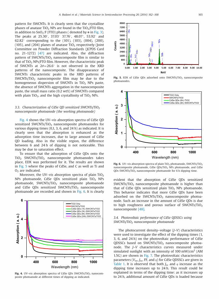
Fig. 5. EDX of CdSe QDs adsorbed onto SWCNTs/TiO2 nanocompositephotoanodes.
4 TiO2 Only SWCNTs/TiO2
A. Badawi et al. / Materials Science in Semiconductor Processing 26 (2014) 162–168 165
pattern for SWCNTs. It is clearly seen that the crystallinephases of anatase TiO2 NPs are found in the TiO2/FTO film,in addition to SnO2:F (FTO) phases ( denoted by n in Fig. 3).The peaks at 25.301, 37.031 37.761, 48.071, 53.921 and62.821 corresponding to the (101), (103), (004), (200),(105), and (204) planes of anatase TiO2 respectively (JointCommittee on Powder Diffraction Standards (JCPDS Cardno. 21-1272) [47] are indicated. Also, the diffractionpattern of SWCNTs/TiO2 nanocomposite film is similar tothat of TiO2 NPs/FTO film. However, the characteristic peakof SWCNTs at 2θ¼26.61 is not observed in the XRDpatterns of the nanocomposite. The disappearance ofSWCNTs characteristic peaks in the XRD patterns ofSWCNTs/TiO2 nanocomposite film may be due to thehomogeneous dispersion of SWCNTs in TiO2 NPs paste,the absence of SWCNTs aggregation in the nanocompositepaste, the small mass ratio (0.2 wt%) of SWCNTs comparedwith plain TiO2, and the high crystallinity of TiO2 NPs.
400 600 800 10000
1
2
3 CdSe QDs (6h) /TiO2 CdSe QDs (6h) /SWCNTs/TiO2
Abs
orpt
ion
( a. u
.)
Wavelength (nm)
Fig. 6. UV–vis absorption spectra of plain TiO2 photoanode, SWCNTs/TiO2
nanocomposite photoanode, CdSe QDs/TiO2 NPs photoanode, and CdSeQDs SWCNTs/TiO2 nanocomposite photoanode for 6 h dipping time.
3.3. Characterization of CdSe QD sensitized SWCNTs/TiO2
nanocomposite photoanode (the working photoanode)
Fig. 4 shows the UV–vis absorption spectra of CdSe QDsensitized SWCNTs/TiO2 nanocomposite photoanodes forvarious dipping times (0,1, 3, 6, and 24 h) as indicated. It isclearly seen that the absorption is enhanced as theadsorption time increases, due to large amount of CdSeQD loading. Also in the visible region, the differencebetween 6 and 24 h of dipping is not noticeable. Thismay be due to saturation effect.
To ensure that the adsorption of CdSe QDs onto theTiO2 SWCNTs/TiO2 nanocomposite photoanodes takesplace, EDX was performed for it. The results are shownin Fig. 5 where the peaks of CdSe, and C as well as Ti andO2 are indicated.
Moreover, the UV–vis absorption spectra of plain TiO2
NPs photoanode, CdSe QDs sensitized plain TiO2 NPsphotoanode, SWCNTs/TiO2 nanocomposite photoanodeand CdSe QDs sensitized SWCNTs/TiO2 nanocompositephotoanode are recorded and shown in Fig. 6. It is clearly
400 600 800 10000
2
4
6 TiO2 Only SWCNTs/TiO2 CdSe QDs (1h) /SWCNTs/TiO2 CdSe QDs (3h) /SWCNTs/TiO2 CdSe QDs (6h) /SWCNTs/TiO2 CdSe QDs (24h) /SWCNTs/TiO2
Abs
orpt
ion
( a. u
.)
Wavelength (nm)
Fig. 4. UV–vis absorption spectra of CdSe QDs SWCNTs/TiO2 nanocom-posite photoanode at different times of dipping as indicated.
evident that the absorption of CdSe QDs sensitizedSWCNTs/TiO2 nanocomposite photoanode is higher thanthat of CdSe QDs sensitized plain TiO2 NPs photoanode.This behavior indicates that more CdSe QDs have beenadsorbed on the SWCNTs/TiO2 nanocomposite photoa-node. Such an increase in the amount of CdSe QDs is dueto high roughness and porous surface of SWCNTs/TiO2
nanocomposite [48].
3.4. Photovoltaic performance of CdSe QDSSCs usingSWCNTs/TiO2 nanocomposite photoanode
The photocurrent density–voltage (J–V) characteristicswere used to investigate the effect of the dipping times (1,3, 6, and 24 h) on the photovoltaic performance of CdSeQDSSCs based on SWCNTs/TiO2 nanocomposite photoa-node. The J–V characteristics curves measured undersimulated sunlight with an intensity of 100 mW/cm2 (AM1.5G) are shown in Fig. 7. The photovoltaic characteristicsparameters (Voc, Jsc, FF, and η) for CdSe QDSSCs are given inTable 1. It is observed that both Jsc and η increase as thedipping time increases up to 24 h. This result could beexplained in terms of the dipping time: as it increases upto 24 h, additional amount of CdSe QDs is loaded because
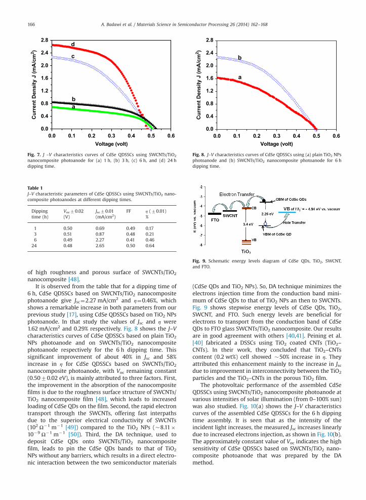
Table 1J–V characteristic parameters of CdSe QDSSCs using SWCNTs/TiO2 nano-composite photoanodes at different dipping times.
Dippingtime (h)
Voc70.02(V)
Jsc70.01(mA/cm2)
FF η (70.01)%
1 0.50 0.69 0.49 0.173 0.51 0.87 0.48 0.216 0.49 2.27 0.41 0.46
24 0.48 2.65 0.50 0.64
0.0 0.1 0.2 0.3 0.4 0.5 0.60.0
0.4
0.8
1.2
1.6
2.0
2.4
2.8
b
Cur
rent
Den
sity
J (m
A/c
m2 )
Voltage (volt)
a
Fig. 8. J–V characteristics curves of CdSe QDSSCs using (a) plain TiO2 NPsphotoanode and (b) SWCNTs/TiO2 nanocomposite photoanode for 6 hdipping time.
Fig. 9. Schematic energy levels diagram of CdSe QDs, TiO2, SWCNT,and FTO.
0.0 0.1 0.2 0.3 0.4 0.5 0.60.0
0.4
0.8
1.2
1.6
2.0
2.4
2.8
b
c
d
Cur
rent
Den
sity
J (m
A/c
m2 )
Voltage (volt)
a
Fig. 7. J –V characteristics curves of CdSe QDSSCs using SWCNTs/TiO2
nanocomposite photoanode for (a) 1 h, (b) 3 h, (c) 6 h, and (d) 24 hdipping time.
A. Badawi et al. / Materials Science in Semiconductor Processing 26 (2014) 162–168166
of high roughness and porous surface of SWCNTs/TiO2
nanocomposite [48].It is observed from the table that for a dipping time of
6 h, CdSe QDSSCs based on SWCNTs/TiO2 nanocompositephotoanode give Jsc¼2.27 mA/cm2 and η¼0.46%, whichshows a remarkable increase in both parameters from ourprevious study [17], using CdSe QDSSCs based on TiO2 NPsphotoanode. In that study the values of Jsc and η were1.62 mA/cm2 and 0.29% respectively. Fig. 8 shows the J–Vcharacteristics curves of CdSe QDSSCs based on plain TiO2
NPs photoanode and on SWCNTs/TiO2 nanocompositephotoanode respectively for the 6 h dipping time. Thissignificant improvement of about 40% in Jsc and 58%increase in η for CdSe QDSSCs based on SWCNTs/TiO2
nanocomposite photoanode, with Voc remaining constant(0.5070.02 eV), is mainly attributed to three factors. First,the improvement in the absorption of the nanocompositefilms is due to the roughness surface structure of SWCNTs/TiO2 nanocomposite film [48], which leads to increasedloading of CdSe QDs on the film. Second, the rapid electrontransport through the SWCNTs, offering fast interpathsdue to the superior electrical conductivity of SWCNTs(102 Ω�1 m�1 [49]) compared to the TiO2 NPs (�8.11�10�9 Ω�1 m�1 [50]). Third, the DA technique, used todeposit CdSe QDs onto SWCNTs/TiO2 nanocompositefilm, leads to pin the CdSe QDs bands to that of TiO2
NPs without any barriers, which results in a direct electro-nic interaction between the two semiconductor materials
(CdSe QDs and TiO2 NPs). So, DA technique minimizes theelectrons injection time from the conduction band mini-mum of CdSe QDs to that of TiO2 NPs an then to SWCNTs.Fig. 9 shows stepwise energy levels of CdSe QDs, TiO2,SWCNT, and FTO. Such energy levels are beneficial forelectrons to transport from the conduction band of CdSeQDs to FTO glass SWCNTs/TiO2 nanocomposite. Our resultsare in good agreement with others [40,41]. Peining et al.[40] fabricated a DSSCs using TiO2 coated CNTs (TiO2–
CNTs). In their work, they concluded that TiO2–CNTscontent (0.2 wt%) cell showed �50% increase in η. Theyattributed this enhancement mainly to the increase in Jscdue to improvement in interconnectivity between the TiO2
particles and the TiO2–CNTs in the porous TiO2 film.The photovoltaic performance of the assembled CdSe
QDSSCs using SWCNTs/TiO2 nanocomposite photoanode atvarious intensities of solar illumination (from 0–100% sun)was also studied. Fig. 10(a) shows the J–V characteristicscurves of the assembled CdSe QDSSCs for the 6 h dippingtime assembly. It is seen that as the intensity of theincident light increases, the measured Jsc increases linearlydue to increased electrons injection, as shown in Fig. 10(b).The approximately constant value of Voc indicates the highsensitivity of CdSe QDSSCs based on SWCNTs/TiO2 nano-composite photoanode that was prepared by the DAmethod.

0.0 0.1 0.2 0.3 0.4 0.5 0.60.0
0.5
1.0
1.5
2.0
2.5
b
c
d
Voltage (Volt )
Cur
rent
den
sity
J (m
A/c
m2 )
a
0.0 0.2 0.4 0.6 0.8 1.00.0
0.5
1.0
1.5
2.0
2.5
Sho
rt c
ircui
t cur
rent
Jsc
(mA
/cm
2 )
of sun
Fig. 10. (a): J–V characteristics curve of CdSe QDSSC using SWCNTs/TiO2 nanocomposite photoanode for 6 h dipping time at a) 30%, b) 50%, c) 80%, andd) 100% of sun; (b) short circuit current density Jsc vs. the percentage of sun.
A. Badawi et al. / Materials Science in Semiconductor Processing 26 (2014) 162–168 167
4. Conclusion
We have synthesized a paste of 0.2 wt% of single walledcarbon nanotubes/Titania (0.2 wt% of SWCNTs/TiO2) nano-composite to fabricate quantum dots sensitized solar cells(QDSSCs) photoanodes. CdSe QDs of 4.52 nm in sizewere prepared and applied as a sensitizer for QDSSCs bydirect adsorption (DA) technique onto 0.2 wt% SWCNTs/TiO2 nanocomposite photoanode. A significant increase(�58%) in the energy conversion efficiency (η) wasachieved in CdSe QDSSCs based on SWCNTs/TiO2 nano-composite as compared to others based on plain TiO2 NPsunder AM 1.5 simulated sunlight. The open circuit voltage(Voc) is unchanged in both solar cells. The increase in η dueto the increase in the photocurrent density (J) of theassembled QDSSCs is attributed to three factors: (i) theimprovement in the absorption of the nanocompositefilms due to increase loading of CdSe QDs on the film, (ii)rapid electron transport through the SWCNTs, offering fastinterpaths due to the superior electrical conductivity ofSWCNTs compared to the TiO2 NPs, and (iii) the DAtechnique, used to deposit CdSe QDs onto SWCNTs/TiO2
nanocomposite films, leads to pin the CdSe QDs to that ofTiO2 NPs without any barriers.
Acknowledgments
The authors wish to thank Taif University for thefinancial support. Quantum Optics Research Group (QORG)at Deanship of Scientific Research- Taif University is alsothanked for their assistance during this work. The Egyp-tian STDF Grant ID 377 support is greatly appreciated.
References
[1] P.V. Kamat, J. Phys. Chem. C 112 (2008) 18737–18753.[2] A. Badawi, N. Al-Hosiny, S. Abdallah, S. Negm, H. Talaat, Sol. Energy
88 (2013) 137–143.[3] S. Kolahi, S. Farjami-Shayesteh, Y. Azizian-Kalandaragh, Mater. Sci.
Semicond. Process. 14 (2011) 294–301.[4] Z. El-Qahtani, A. Badawi, K. Easawi, N. Al-Hosiny, S. Abdallah, Mater.
Sci. Semicond. Process. 20 (2014) 68–73.
[5] A. Badawi, K. Easawi, N. Al-Hosiny, S. Abdallah, Mater. Sci. Appl. 5(2014) 27–32.
[6] Y. Xie, S.H. Yoo, C. Chen, S.O. Cho, Mater. Sci. Eng. B 177 (2012)106–111.
[7] K. Tvrdy, P.A. Frantsuzov, P.V. Kamat, Proc. Natl. Acad. Sci. USA 108(2011) 29–34.
[8] H. Chen, W. Li, H. Liu, L. Zhu, Electrochem. Commun. 13 (2011)331–334.
[9] A. Salant, M. Shalom, I. Hod, A. Faust, A. Zaban, U. Banin, ACS Nano 4(2010) 5962–5968.
[10] A. Kongkanand, K. Tvrdy, K. Takechi, M. Kuno, P.V. Kamat, J. Am.Chem. Soc. 130 (2008) 4007–4015.
[11] J. Kim, H. Choi, C. Nahm, J. Moon, C. Kim, S. Nam, D.-R. Jung, B. Park,J. Power Sources 196 (2011) 10526–10531.
[12] S. Emin, S.P. Singh, L. Han, N. Satoh, A. Islam, Sol. Energy 85 (2011)1264–1282.
[13] A. Tubtimtae, K.-L. Wu, H.-Y. Tung, M.-W. Lee, G.J. Wang, Electro-chem. Commun. 12 (2010) 1158–1160.
[14] S. Abdallah, N. Al-Hosiny, A. Badawi, J. Nanomater. 2012 (2012) 6.[15] J. Jiao, Z.-J. Zhou, W.-H. Zhou, S.-X. Wu, Mater. Sci. Semicond.
Process. 16 (2013) 435–440.[16] F. Zhao, G. Tang, J. Zhang, Y. Lin, Electrochim. Acta 62 (2012) 396–401.[17] A. Badawi, N. Al-Hosiny, S. Abdallah, H. Talaat, Mater. Sci.-Pol. 31
(2013) 6–13.[18] D.R. Pernik, K. Tvrdy, J.G. Radich, P.V. Kamat, J. Phys. Chem. C 115
(2011) 13511–13519.[19] X. Wang, H. Zhu, Y. Xu, H. Wang, Y. Tao, S. Hark, X. Xiao, Q. Li, ACS
Nano 4 (2010) 3302–3308.[20] S. Kitada, E. Kikuchi, A. Ohnob, S. Aramakib, S. Maenosono, Solid
State Commun. 149 (2009) 1853–1855.[21] B.-R. Hyun, Y.-W. Zhong, A.C. Bartnik, L. Sun, H.D. Abrun, F.W. Wise, J.
D. Goodreau, J.R. Matthews, T.M. Leslie, N.F. Borrelli, ACS Nano 2(2008) 2206–2212.
[22] Y. Liu, J. Wang, Thin Solid Films 518 (2010) e54–e56.[23] P. Yu, K. Zhu, A.G. Norman, S. Ferrere, A.J. Frank, A.J. Nozik, J. Phys.
Chem. B 110 (2006) 25451–25454.[24] C.-C. Wang, L.-C. Chen, T.-C. Wang, J. Optoelectron. Adv. Mater. 11
(2009) 834–837.[25] A. Tubtimtae, M.-W. Lee, G.-J. Wang, J. Power Sources 196 (2011)
6603–6608.[26] I. Mora-Ser´o, S. Gim´enez, T. Moehl, F. Fabregat-Santiago,
T. Lana-Villareal, R. G´omez, J. Bisquert, Nanotechnology (2008)424007.
[27] S. Ruhle, M. Shalom, A. Zaban, ChemPhysChem 11 (2010) 2290–2304.[28] N. Guijarro, T. Lana-Villarreal, I. Mora-Seró, J. Bisquert, R. Gómez,
J. Phys. Chem. C 113 (2009) 4208–4214.[29] J.H. Bang, P.V. Kamat, ACS Nano 3 (2009) 1467–1476.[30] S. Giménez, I. Mora-Seró, L. Macor, N. Guijarro, T. Lana-Villarreal,
R. Gómez, L.J. Diguna, Q. Shen, T. Toyoda, J. Bisquert, Nanotechnology20 (2009) 295204.
[31] J. Yan, M.J. Uddin, T.J. Dickens, O.I. Okoli, Sol. Energy 96 (2013)239–252.
[32] H. Chang, T.-J. Hsieh, T.-L. Chen, K.-D. Huang, C.-S. Jwo, S.-H. Chien,Mater. Trans. 50 (2009) 2879–2884.
[33] H. Anwar, A.E. George, I.G. Hill, Sol. Energy 88 (2013) 129–136.

A. Badawi et al. / Materials Science in Semiconductor Processing 26 (2014) 162–168168
[34] Y. Choi, Y. Kim, S.-G. Park, Y.-G. Kim, B.J. Sung, S.-Y. Jang, W. Kim, Org.Electron. 12 (2011) 2120–2125.
[35] J. Al-Osaimi, N. Alhosiny, A. Badawi, S. Abdallah, Int. J. Eng. Technol.IJET-IJENS 13 (2013) 77–79.
[36] E.R. Morales, N.R. Mathews, D. Reyes-Coronado, C.R. Magaña,D.R. Acosta, G. Alonso-Nunez, O.S. Martinez, X. Mathew, Sol. Energy86 (2012) 1037–1044.
[37] J.Y. Ahn, J.H. Kim, K.J. Moon, J.H. Kim, C.S. Lee, M.Y. Kim, J.W. Kang,S.H. Kim, Sol. Energy 92 (2013) 41–46.
[38] G. Khurana, S. Sahoo, S.K. Barik, R.S. Katiyar, J. Alloys Compd. 578(2013) 257–260.
[39] S.U. Lee, W.S. Choi, B. Hong, Sol. Energy Mater. Sol. Cells 94 (2010)680–685.
[40] Z. Peining, A.S. Nair, Y. Shengyuan, P. Shengjie, N.K. Elumalai,S. Ramakrishna, J. Photochem. Photobiol. A: Chem. 231 (2012)9–18.
[41] J. Yu, J. Fan, B. Cheng, J. Power Sources 196 (2011) 7891–7898.[42] D.V. Talapin, S. Haubold, A.L. Rogach, A. Kornowski, M. Haase,
H. Weller, J. Phys. Chem. B 105 (2001) 2260–2263.
[43] G. Syrrokostas, M. Giannouli, P. Yianoulis, Renew. Energy 34 (2009)1759–1764.
[44] O. Madelung, Semiconductors: Data Handbook, 3rd ed. Springer-Verlag, Berlin, 2004.
[45] L. Brus, J. Phys. Chem. 90 (1986) 2555–2560.[46] Parak, W.J., Manna, L., Simmel, F.C., Gerion, D., Alivisatos, P.,
Quantum Dots, in: Nanoparticles: From Theory to Application,G. Schmid (Ed.) Wiley-VCH Verlag GmbH & Co. KGaA, Weinheim,FRG, 2005, http://dx.doi.org/10.1002/3527602399.ch2.
[47] S. Ngamta, N. Boonprakob, N. Wetchakun, K. Ounnunkad,S. Phanichphant, B. Inceesungvorn, Mater. Lett. 105 (2013) 76–79.
[48] E.S. Lee, K.M. Lee, S.I. Yoon, Y.G. Ko, D.H. Shin, Curr. Appl. Phys. 13(Suppl. 2) (2013) S26–S29.
[49] P.-C. Ma, N.A. Siddiqui, G. Marom, J.-K. Kim, Composites Part A 41(2010) 1345–1367.
[50] K. Pomoni, M.V. Sofianou, T. Georgakopoulos, N. Boukos, C. Trapalis,J. Alloys Compd. 548 (2013) 194–200.