Single-step deposition of high mobility graphene at ...yehgroup/documents/NatComm_PECVD... ·...
20
1 Single-step deposition of high mobility graphene at reduced temperatures D. A. Boyd, 1 W.‐H. Lin, 2 C.‐C. Hsu, 1,3 M. L. Teague, 1,3 C.‐C. Chen, 1,3 Y.‐Y. Lo, 4 W.‐Y. Chan, 5 W.‐B. Su, 5 T.‐C. Cheng, 4 C.‐S. Chang, 5 C.‐I. Wu, 4 N.‐C. Yeh 1,3,6 * 1 Department of Physics, California Institute of Technology, Pasadena, CA 91125, USA. 2 Department of Applied Physics, California Institute of Technology, Pasadena, CA 91125, USA. 3 Institute of Quantum Information and Matter, California Institute of Technology, Pasadena, CA 91125, USA. 4 Graduate Institute of Photonics and Optoelectronics and Department of Electrical Engineering, National Taiwan University, Taipei, Taiwan. 5 Institute of Physics, Academia Sinica, Nankang, Taipei, Taiwan. 6 Kavli Nanoscience Institute, California Institute of Technology, Pasadena, CA 91125, USA. * e-mail: Nai-Chang Yeh ([email protected]) Current methods of chemical vapor deposition (CVD) of graphene on copper are complicated by multiple processing steps and the need for high temperatures in both preparing the copper and inducing subsequent film growth. Here we demonstrate a plasma-enhanced CVD (PECVD) chemistry that enables the entire process to take place in a single step, at reduced temperatures (< 420 C), and in a matter of minutes. Growth on copper foils is found to nucleate from arrays of well-aligned domains, and the ensuing films possess sub-nanometer smoothness, excellent crystalline quality, low strain, few defects, and room-temperature electrical mobility up to (6.01.0)×10 4 cm 2 V - 1 s -1 , better than that of large, single-crystalline graphene derived from thermal CVD- growth. These results indicate that elevated temperatures and crystalline substrates are not necessary for synthesizing high-quality graphene.
-
Upload
truongtram -
Category
Documents
-
view
220 -
download
2
Transcript of Single-step deposition of high mobility graphene at ...yehgroup/documents/NatComm_PECVD... ·...
1
Single-step deposition of high mobility graphene at reduced temperatures
D.A.Boyd,1W.‐H.Lin,2C.‐C.Hsu,1,3M.L.Teague,1,3C.‐C.Chen,1,3Y.‐Y.Lo,4W.‐Y.Chan,5
W.‐B.Su,5T.‐C.Cheng,4C.‐S.Chang,5C.‐I.Wu,4N.‐C.Yeh1,3,6*
1Department of Physics, California Institute of Technology, Pasadena, CA 91125, USA. 2Department of Applied Physics, California Institute of Technology, Pasadena, CA 91125, USA. 3Institute of Quantum Information and Matter, California Institute of Technology, Pasadena, CA 91125, USA. 4Graduate Institute of Photonics and Optoelectronics and Department of Electrical Engineering, National Taiwan University, Taipei, Taiwan. 5Institute of Physics, Academia Sinica, Nankang, Taipei, Taiwan. 6Kavli Nanoscience Institute, California Institute of Technology, Pasadena, CA 91125, USA. *e-mail: Nai-Chang Yeh ([email protected]) Current methods of chemical vapor deposition (CVD) of graphene on copper are
complicated by multiple processing steps and the need for high temperatures in both
preparing the copper and inducing subsequent film growth. Here we demonstrate a
plasma-enhanced CVD (PECVD) chemistry that enables the entire process to take place
in a single step, at reduced temperatures (< 420 C), and in a matter of minutes. Growth
on copper foils is found to nucleate from arrays of well-aligned domains, and the
ensuing films possess sub-nanometer smoothness, excellent crystalline quality, low
strain, few defects, and room-temperature electrical mobility up to (6.01.0)×104 cm2V-
1s-1, better than that of large, single-crystalline graphene derived from thermal CVD-
growth. These results indicate that elevated temperatures and crystalline substrates are
not necessary for synthesizing high-quality graphene.
2
Introduction
Much progress has been made in growing large-area graphene by means of thermal
chemical vapor deposition (CVD) based on catalytic dehydrogenation of carbon precursors
on copper 1–4. However, in many instances it is desirable to avoid multiple steps2 and high
temperatures (~1000 C) employed in thermal-CVD growth. In particular, the conditions for
the critical removal of the native copper oxide and the subsequent film growth are dissimilar
enough to necessitate separate process steps. Moreover, high processing temperatures
restricts the types of devices and processes where CVD can be applied and can also result in
film irregularities that compromise the graphene quality itself 4. Thermally derived strain and
topological defects5-8, for example, can induce giant pseudo-magnetic fields and charging
effects, giving rise to localization and scattering of Dirac fermions7,8 and diminishing the
electrical properties.
A variant of thermal CVD, called plasma-enhanced CVD (PECVD), has been widely
used for depositing many allotropes of carbon, most notably diamond films. The plasma can
provide a rich chemical environment, including a mixture of radicals, molecules and ions
from a simple hydrogen-hydrocarbon feedstock9, allowing for lower deposition
temperatures10 and faster growth than thermal CVD. The ability of the plasma to concurrently
support multiple reactive species is a key advantage. However, the quality of PECVD-grown
graphene to date has not been significantly better than that of thermal CVD10,11,12.
Here we demonstrate a PECVD process that encompasses both the preparation of the
copper and growth of graphene in a single step. The addition of cyano radicals, which are
known to etch copper at room temperature13, to a hydrogen-methane plasma is found to
produce a chemistry whereby the native oxide is removed, the copper is smoothly etched, and
growth of well-aligned graphene ensues. Etching of the copper substrate is found to be self-
3
limiting, allowing etching and growth steps to proceed in tandem under the same chemistry.
The entire process occurs in a matter of minutes without active heating, and the resulting
graphene films exhibit high electrical mobility and few structural defects. Our results indicate
that elevated temperatures, crystalline substrates, and long process times are not necessary for
synthesizing high-quality graphene.
Results
Description and characterization of process. The PECVD growth process is schematically
illustrated in Fig. 1a-c and further described in Methods and Supplementary Figure 1. Copper
was directly exposed to a low-pressure, microwave hydrogen plasma containing trace
amounts of cyano radicals (Supplementary Figure 2), methane and nitrogen (Supplementary
Figure 3), as detailed in Supplementary Note 1. Removal of the native oxide and smoothing
of the copper typically occurred within two minutes of igniting the plasma (Fig. 1a).
Nucleation of graphene ensued on both sides of the substrate (Fig. 1b). With continued
exposure to the plasma, disordered graphite and monolayer graphene covered the top and
bottom sides, respectively (Fig. 1c). Copper deposits were found on both the process tube and
the sample holder after successful growth runs (Fig. 1d), whereas runs with little copper
etching did not produce optimal films. Optical microscopy showed that the graphene on the
top surface of copper was always randomly pitted after growth (Fig. 1e), while that on the
bottom surface was smooth (Fig. 1f). Scanning tunneling microscopy (STM) measurements
of the surface topography of graphene on the bottom side of Cu revealed sub-nanometer
flatness for samples grown on Cu foils and single crystalline Cu (100) and Cu (111), (Fig. 1g-
i and Supplementary Figure 5a-c). Nitrogen incorporation into the graphene, as measured by
x-ray photoemission spectroscopy (XPS), Supplementary Figure 4a-b, was found to be below
the detection limit14 of 0.1 at.%.
4
We found that the occurrence of PECVD-graphene growth was largely insensitive to
the gas temperature of the plasma. The maximum gas temperature of the plasma determined
by a thermocouple sheathed in boron nitride was found to be 160C (425C) for 10W (40W)
plasma power, which decayed by more than 120C (250C) within ~1 cm from the center of
the plasma. The maximum temperature of the copper substrate Ts was measured using the
melting points of known solids on top of a copper substrate subjected to the plasma. We
found that at 40 W plasma power, lead melted whereas zinc did not, indicating that the
maximum Cu substrate temperature was within the range of 327.5 C < Ts < 419.5 C.
Further, we were able to fabricate more than 300 high-quality large-area graphene samples by
PECVD within 5~20 minutes in a single-step by using plasma power varying between 10 and
40 W. The typical substrate size was (8×13) mm2 ~ 1 cm2. Although the plasma produced by
the Evenson cavity was not uniform in intensity over the length of the sample, graphene was
found to cover the entire substrate and exhibited consistent quality over the entire film on the
bottom side, indicating that the growth was not temperature sensitive and could occur over a
range of temperatures. We expect that the sample size should be scalable in a larger cavity
under the same growth conditions. The localized nature of the plasma source also allowed
multiple samples to be prepared individually in the same process tube without changing
conditions or breaking vacuum by simply translating the Evenson cavity.
Nucleation and growth. The time evolution in the Raman spectra of PECVD-graphene on
opposite sides of copper foils during growth is shown in Fig. 1j-k. Spectra from the top side
(Fig. 1j) featured the D-band, an indicator of edges or disorder in graphene and graphite; the
G-band, a feature common to both graphene and graphite; and the 2D-band, a unique feature
to graphene. The D-band was prominent throughout, while the 2D-band decreased and
disappeared with time, indicating the formation of disordered graphite, which is consistent
with optical images of the top side (Fig. 1e). In contrast, spectra from the bottom side (Fig.
5
1k) showed that the D-band decreased and eventually vanished with increasing growth time
while the relative intensities of 2D and G-bands indicate the formation of monolayer
graphene15,16,17,18, as described in Methods and Supplementary Figure 6a-6b. This behavior is
consistent with growth and eventual coalescence of graphene domains wherein the D-band
associated with the edge states of the domains diminished19. A comparison of the graphene
from the top and bottom sides indicate that increased mass flux and direct plasma exposure
adversely affected the film quality, and hereafter we focus our studies on PECVD graphene
grown on the bottom side of Cu.
Scanning electron microscopy (SEM) images taken shortly after the onset of graphene
growth on copper foil (Fig. 2a-d) revealed dense, linear arrays of hexagonal graphene
domains that extended across the copper grains. With increasing growth time, the well-
aligned graphene domains coalesced seamlessly into a monolayer graphene with few defects.
Shown in Fig. 2e-f are the 2D/G and D/G intensity ratio maps of a (100100) m2 area of an
as-deposited graphene sample on Cu, respectively. The average 2D/G intensity ratio (I2D/IG)
is ~2 and only 5% of the mapped area show any measurable D-band. Histograms of the
(I2D/IG) and (ID/IG) maps are provided in Supplementary Figure 6a and 6b, respectively.
Although the number of graphene layers may be determined from the full-width-half-
maximum (FWHM) of the 2D-band24, the absolute value of the FWHM can be affected by
the underlying substrate25. To avoid such complications, Raman maps of PECVD graphene
transferred from Cu to Si/SiO2 are provided in Supplementary Figure 7a-7d and detailed in
Methods and Supplementary Note 2. The average value of the FWHM of the 2D-band, which
was fit to a single Lorentzian, was 28.8 cm1, and the average ratio (I2D/IG) = 2.7, both
consistent with the figure of merit for monolayer graphene15,16,17,18,24.
6
High-resolution (~ 1 nm) atomic force microscopy (AFM) and SEM studies over
multiple (100100) m2 areas of an annealed monolayer graphene sample20, which was
transferred to single crystalline sapphire with a polymer-free technique21, indicated no
discernible grain boundaries. With an increase of growth time, small adlayers began to
develop on top of the first layer in an aligned fashion, as exemplified by the SEM images in
Fig. 2h-j. These findings, which are supported by Fig. 1k, indicate that the growth of
PECVD-graphene on copper foils proceeded by nucleation and growth of well-aligned
domains22,23 that eventually coalesced into a large single crystalline sheet, and the subsequent
growth of the second layer with increasing time followed a similar mechanism (Fig. 2h-j).
Strain and structural ordering. The biaxial strain ll tt in the PECVD-graphene on Cu
can be estimated by considering the Raman frequency shifts 0m m m and the
Grϋneisen parameter biaxm :15,26
biax mm 0
m ll tt
, (1)
where m (= G, 2D) refers to the specific Raman mode. Using the parameter biax2D 2.7 , the
strain distribution over an area of (100100) m2 is exemplified in Fig. 2g, showing
consistently low strain characteristics, with an average strain ~ 0.07% for m = 2D.
Overall, a general trend of downshifted G-band and 2D-band15 was found for all
PECVD-graphene relative to thermal CVD-grown graphene on the same substrate, as
exemplified in Supplementary Figure 8a-c for comparison of PECVD- and as-grown thermal
CVD-graphene on substrates of Cu foil, Cu (100) and Cu (111). The consistent frequency
downshifts for all PECVD-graphene indicate reduction in the averaged biaxial strain. Further,
absence of the D-band in most spectra suggests that the samples were largely free of
7
disorder/edges on the macroscopic scale, which is further corroborated by detailed spatial
mapping of the Raman spectra over an area of (100100) m2 in Fig. 2e-f.
Our PECVD-graphene samples also exhibited well-ordered honeycomb atomic
lattices, which is unique to monolayer graphene, as evidenced by the STM images of samples
on Cu foil (Fig. 3a-c), Cu (100) (Fig. 3e-g), and Cu (111) (Fig. 3i-k). The long-range
structural ordering was further corroborated by the sharp Fourier transformation (FT) of STM
topographies, as exemplified in Fig. 3d,h,l. The FT spectra demonstrated dominantly
hexagonal lattices for all PECVD-graphene. Samples grown on Cu single crystals further
exhibited Moiré patterns, as manifested by the second set of smaller Bragg diffraction peaks.
Simulations (see Methods) indicated the Moiré pattern (a parallelogram) in the FT of Fig. 3h
for graphene on Cu (100), was the result of a square lattice at approximately an angle ~
(122) relative to the honeycomb lattice (Supplementary Figure 9a), whereas the Moiré
pattern (a smaller hexagon) in the FT of Fig. 3l suggested that the Cu (111) hexagonal lattice
was at ~ (62) relative to the graphene lattice (Supplementary Figure 9b). These STM
measurement over multiple samples and multiple areas per sample confirm the predominance
of monolayer graphene and the absence of discernible bilayer graphene in our PECVD-grown
samples.
The STM topography was further employed to analyze strain at the microscopic scale.
For a local two-dimensional displacement field 0ˆ ˆ x yu x u yu r r , where r and r0 denote
the actual position of a carbon atom and its equilibrium position in ideal graphene,
respectively27, the compression/dilation strain is given by x y xx yyu x u y u u ,
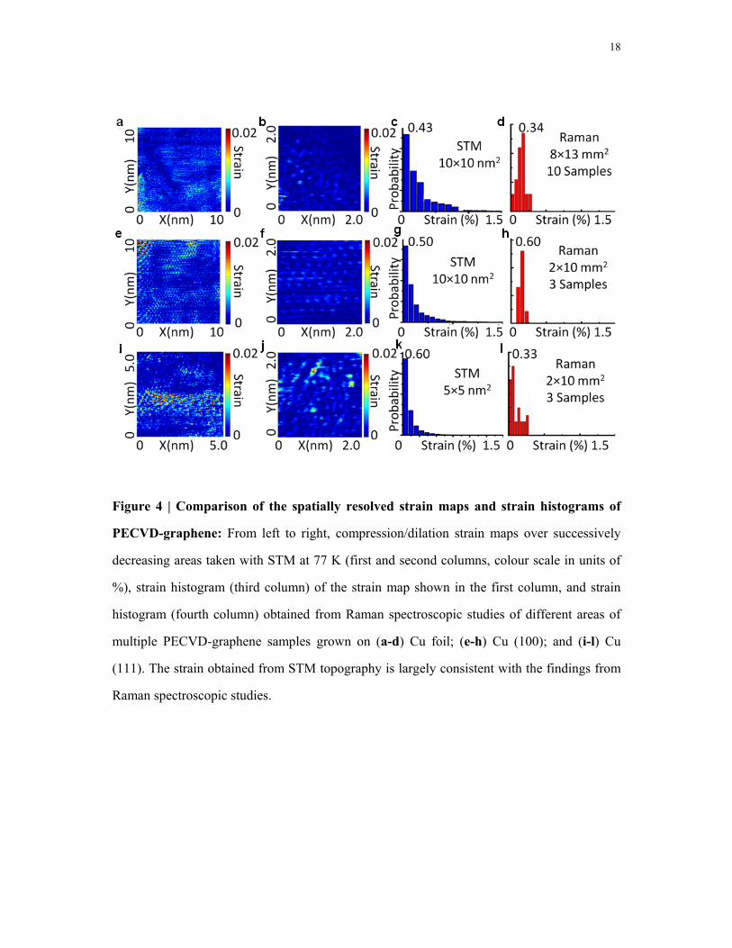
which is proportional to the biaxial strain5,7,8. Using the topographies shown in Fig. 3a-c, we
obtained the spatial strain maps for PECVD-graphene on Cu foil, Cu (100) and Cu (111)
substrates over successively decreasing areas in Fig. 4a-b, 4e-f and 4i-j, respectively. The
8
corresponding strain histograms are given in Fig. 4c,g,k. The PECVD-graphene exhibited
low and relatively homogeneous strain distributions. Further comparison with the
macroscopic strain obtained from a collection of Raman spectra taken on different areas of
multiple PECVD-graphene samples are summarized by the strain histograms in Fig. 4d,h,l.
There is overall consistency between microscopic STM studies and macroscopic Raman
spectroscopic studies, revealing low strain for all PECVD-graphene.
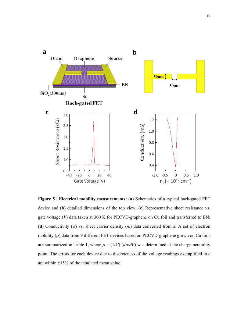
Electrical properties. The electrical mobility () of PECVD-graphene was determined by
studying back-gated field-effect-transistor (FET) devices28,29. Graphene samples were first
transferred to hexagonal BN thin films on 300 nm SiO2/Si substrates using a polymer-free
method21, and then lithographically processed into a geometry shown in Fig. 5a-b. The sheet
resistance of graphene as a function of the back-gate voltage (V) and the corresponding
conductivity () vs. sheet carrier density (ns) were measured at 300 K, as exemplified in Fig.
5c-d. The electrical mobility was obtained from the derivative of the Drude formula28 near
the charge neutrality point:
1 C d dV , (2)
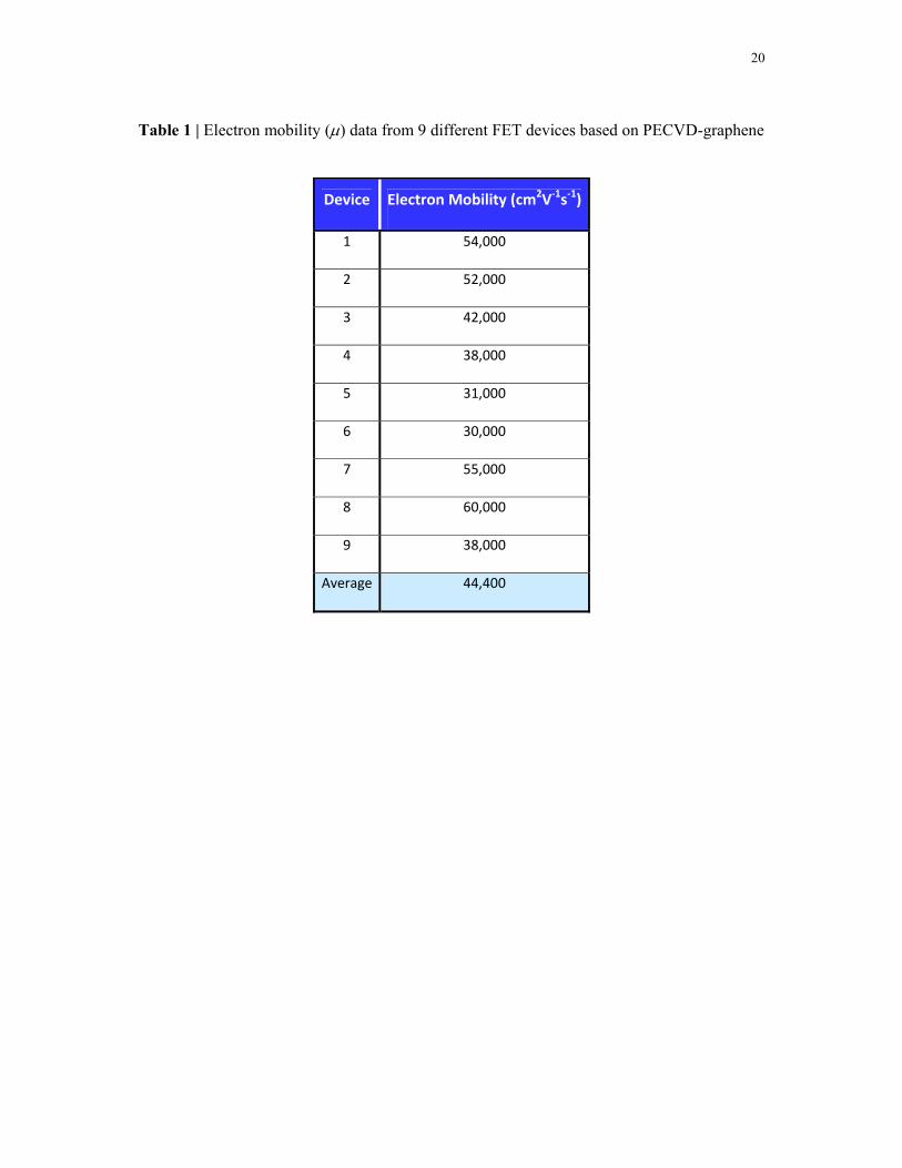
where C denotes the capacitance of the device. The electrical mobility obtained from 9
different devices was found to range from (3.00.5)×104 cm2V-1s-1 to (6.01.0)×104 cm2V-1s-1
for electrons, as summarized in Table 1, and from (1.20.2)×104 cm2V-1s-1 to (3.50.5)×104
cm2V-1s-1 for holes, where the errors represented variations in determining the (d /dV) slope
due to the discreteness of voltage readings. These values are comparable to those obtained on
large, single crystalline thermal CVD-grown graphene on BN, the latter yielded ~ 4×10⁴ to
6×104 cm2V-1s-1 at 1.7 K and ~ 1.5×10⁴ to 3×104 cm2V-1s-1 at 300 K.2
9
It is worth commenting on the accuracy of mobility values obtained by the two-
terminal configuration depicted in Fig. 5a-b. The contact resistance between electrode and
graphene was determined by the Transmission Line Models (TLM) method and was found to
be typically ~ 10 for all devices. In contrast, the sheet resistance of graphene was typically
more than 1 k near the charge neutrality point, which was about 2 orders of magnitude
larger than the contact resistance. Therefore, the contact resistance would not affect the
accuracy of the mobility significantly. Additional measurements by patterning some of the
PECVD-graphene into the four-point configuration revealed that the differences in mobility
thus determined was less than 2-3 % from those obtained by means of the two-point method.
Discussion
Experience with diamond PECVD lends understanding to the observed nucleation and
growth of aligned graphene domains presented here. In the case of diamond growth, it is
known to involve a competition between growth by carbon radicals (most notably methyl
radicals) and etching of amorphous or disordered carbon by atomic hydrogen. The process
conditions used in our experiments are similar to those of microwave CVD growth of
diamond thin films. Therefore, it is not unreasonable to expect that our PECVD growth of
graphene also proceeds in a competitive manner.30 Further, diamond is known to
preferentially nucleate via surface defects31,32, and the aligned domains in our work were
found to be commensurate with the inherent machine marks on the as-received copper foils.
Although the copper surface is smoothed during the PECVD process, remnants of the defects
are likely because the process temperature is low. For comparison, aligned nucleation was not
observed on single-crystal copper, which contains no marks. For thermal CVD growth of
large, single-crystal graphene2, it is preferable to have smooth, defect-free substrates and
restricted nucleation. Therefore, multiple steps to prepare the substrates prior to thermal CVD
10
growth and post annealing after the growth to optimize the sample are necessary2. In contrast,
graphene with equivalent or even better mobility can be achieved by the one-step PECVD
process described in this work. This PECVD process is also scalable11, occurs at CMOS
compatible temperatures, and avoids complications with multiple steps and post-processing.
Overall, our findings of the guided PECVD growth process not only shed new light on the
growth kinetics of graphene but also open up a new pathway to large-scale, excellent quality
and fast graphene fabrication. In particular, this one-step PECVD process potentially allows
graphene to be used as-deposited, making it amenable for integration with complementary
materials and technology.
Methods
Experimental setup. The experimental setup is summarized in Supplementary Figure 1, which consists of plasma, vacuum, and gas delivery systems. The plasma system (Opthos Instruments Inc.) consists of an Evenson cavity and a power supply (MPG-4), which provides an exciting frequency of 2450 MHz. The Evenson cavity mates with a quartz tube of inner and outer diameters of 10 mm and 12.5 mm, respectively. The vacuum system is comprised of a mechanical roughing pump, two capacitance manometers, a pressure control valve, and a measurement control system. There is a fore-line trap between the vacuum pump and the MKS 153 control valve. The gas delivery system consists of mass flow controllers (MFCs) for H2, CH4, and Ar. A bakeable variable leak valve is placed before the methane MFC, and there is a leak valve for N2. A gas purifier was place before the variable leak valve on the methane line. Quarter-turn, shut-off valves are placed directly after each of the MFCs. The system pressure and gas flows are monitored and controlled through the controller via a LabView interface. A residual gas analyzer (RGA) is used to monitor the exhaust gas. Detailed PECVD growth procedure and information. The copper substrates were placed on a quartz flat inside of quartz tube. A typical substrate size was (8×13) mm2. The tube was evacuated to 25 to 30 mTorr. A 2-5 sccm flow of room temperature hydrogen gas with 0.4% methane and a comparable amount of nitrogen gas was added and the pressure was controlled at 500 mTorr. The addition of methane to the gas flow was controlled by a precision leak valve, and a typical concentration, as measured by gas chromatography, was 0.4 %. The initially low vacuum conditions (~ 25 mTorr) provided sufficient partial pressures of nitrogen (atmospheric) for the PECVD process. (We note that a leak valve for including purified nitrogen was added to the setup to study the effects of increased nitrogen partial pressures.) Typical partial pressures measured by residual gas analysis (RGA) are as follows:
N2 (Mass 28): 6.9 × 10⁸ Torr CH4 (Mass 16): 1.5 × 10⁷ Torr

11
O2 (Mass 32): 5.4 × 10⁹ Torr H2O (Mass 18): 1.2 × 10⁶ Torr CO2 (Mass 44): 2.3 × 10⁸ Torr From these values we estimate that the concentration of nitrogen in the gas flow is typically on the same order as that of methane. The PECVD process was found to be highly sensitive to the relative amounts of methane and nitrogen. Excessive methane mixtures resulted in no etching, while excessive nitrogen mixtures would result in excessive etching of the copper. Slight adjustments to the methane concentration could be made via either optical emission spectroscopy (OES) or residual gas analysis (RGA). A low-power (ranging from 10 to 40 W) cold hydrogen plasma was formed over the copper substrate using an Evenson cavity. Exposure of copper substrates to the plasma enabled continuing etching and cleansing of the copper surface during the graphene growth process. The gas temperature inside the plasma was measured using a thermocouple sheathed in boron nitride. The thermocouple was placed in the plasma above the sample and could be translated along the tube. The peak gas temperature measured in plasma treatment was 160 C at 10 W and 425 C at 40 W, and the gas temperature profile decreased rapidly (by 120 C at 10 W and 425 C at 40 W within 1 cm) from the peak value. The maximum temperature of the copper substrate Ts was measured using the melting point of known solids, lead and zinc, and found to be within the range of 327.5 C < Ts < 419.5 C at 40 W. Typically after 5 to 20 minutes of direct exposure to the plasma, a large-area monolayer graphene formed on the backside of copper substrates while the front side of the substrates was coated with disordered graphite. Upon the completion of graphene growth, the plasma was extinguished, and the gas flows were stopped. The process tube was then evacuated and back filled with Ar, and the substrate with graphene coating was subsequently removed. Copper deposition was visible on the inside of the tube and on the sample holder as the result of plasma etching of the copper substrates. Analysis of monolayer graphene using Raman spectroscopy. The Raman maps shown in Fig. 2e-f of the manuscript for PECVD-graphene on Cu were collected with Renishaw InVia @ 532 nm, and the spectra were taken at 2 m per pixel steps over an area of (100 100) m2 for a total of 2601 spectra. Similarly, the Raman maps in Supplementary figure 7a-b for PECVD-graphene transferred to SiO2 were taken at 2 m per pixel steps over an area of (160 150) m2. Each spectrum was smoothed and the broad background from the copper fluorescence was removed, and the peak locations and intensities for the D, G, and 2D features were extracted using a Matlab script. The relative intensities of the 2D and G-band and those of the D and G-band are presented Fig. 2e-f, and histograms of the ratio values and the FWHM linewidth of the 2D band of our PECVD-grown graphene on Cu and commercial thermal CVD-grown graphene on Cu are shown in Supplementary figure 6a-e. The predominant (ID/IG) ~ 0 value of the graphene sample shown in Supplementary figure 6a indicates negligible defects, whereas the histogram of the 2D/G intensity ratio (I2D/IG) in Supplementary figure 6b reveals that the average of the (I2D/IG) value is ~ 2, which agrees with the figure of merit (I2D/IG) > 1 for monolayer graphene15,16,17,18. This notion of predominantly monolayer graphene described in this work is further corroborated by detailed studies of a PECVD-graphene sample transferred from Cu to a SiO2 substrate, which prevents the complication of slow oxidation of the Cu substrate that could
12
result in graphene linewidth broadening with time due to the influence of the substrate (see Supplementary Note 2). As shown in Supplementary Figure 7a-d, a large spatial map over an area of (160150) m2 revealed a mean FWHM value = 28.8 cm1 for the 2D-band and a mean value (I2D/IG) = 2.7, both are consistent with predominantly monolayer graphene if we use either the criterion of 2D-band FWHM < 30 cm1 as the figure of merit for monolayer graphene on SiO2,
24 or the criterion (I2D/IG) > 1 for monolayer graphene on various substrates15,16,17,18. Simulations. Simulations of the Moiré patterns and the corresponding Fourier transformation (FT) were made by means of Matlab. We generated the triangular and cube lattices by using cosine square function and the hexagonal lattice by displacement of two triangular lattice functions. The lattice constant for the ideal 2D honeycomb structure of graphene is 0.2461 nm and that for the ideal Cu FCC lattice is 0.3615 nm, which has a corresponding lattice
constant (0.3615 2) 0.2556 nm for the triangular lattice in the 111 direction and the square lattice in the 100 direction. To simulate realistic STM imaging of the Moiré pattern for a given relative angle between the top graphene layer and the underlying Cu lattice, we assume the resulted topological function G(x,y) has the following form:
C ,C Cu, , , ,k G x yG x y G x y r e G x y , (3)
where 0 < r 1, GC(x,y) is the graphene honeycomb lattice function and GCu(x,y,) is the copper layer function which could be either the triangular lattice for Cu (111) or the cubic lattice for Cu (100). Both functions are normalized with maximum 1 and minimum 0. We use
the exponent C ,k G x ye in equation (3) to simulate the rapid decay of the tunneling current contribution from the copper atom directly under a carbon atom in the top graphene layer, where k is parameter that controls the decay rate and was chosen to be 2 ~ 4. Even for exposed copper atoms without any carbon atom directly positioning above, the signal from copper is expected to be attenuated by a ratio r due to a larger distance from the STM tip to the copper layer. The above expression ensures that contributions from copper atoms directly under carbon atoms are much reduced due to deflection of tunneling electrons, whereas those from exposed copper atoms are only attenuated by a coefficient r. The matching between simulations and the Fourier transform (FT) of graphene on Cu (100) lattice data is judged by the angle of inner parallelism. At = (122), the angle of the inner parallelism appear to match the experimental result in Fig. 3h, as shown in by the real space Moiré pattern (left panel) and the corresponding FT (right panel) in Supplementary Figure 9a. In contrast, the matching between simulations and the FT of graphene on Cu (111) data is based on the size of inner hexagon relative to that of the outer hexagon for graphene lattice. In fact, there are actually two inner hexagons according to the simulations, as exemplified in the FT of the Moiré pattern in Supplementary Figure 9b for = (62). However, empirically only the larger inner hexagon is visible (Fig. 3l). We attribute this discrepancy to the intense DC signal from the zone center of the FT spectra, which overwhelms the signal of the smaller inner hexagon and so becomes invisible upon our removal of the DC signal.
13
References
1. Li, X. et al. Large-area synthesis of high-quality and uniform graphene films on copper foils. Science 324, 1312 (2009).
2. Hao, Y. et al. The role of surface oxygen in the growth of large single-crystal graphene on copper. Science 342, 720 (2013).
3. Yan, Z. et al. Toward the synthesis of wafer-scale single-crystal graphene on copper foils. ACS Nano 6, 9110 (2012).
4. Mun, J. H. & Cho, B. J. Synthesis of monolayer graphene having a negligible amount of wrinkles by stress relaxation. Nano Lett. 13, 2496 (2013).
5. Guinea, F., Katsnelson, M. I., Geim, A. K. Energy gaps and a zero-field quantum Hall effect in graphene by strain engineering. Nat. Phys. 6, 30 (2010).
6. Levy, N. et al. Strain-induced pseudo magnetic fields greater than 300 Tesla in graphene nanobubbles. Science 329, 544 (2010).
7. Yeh, N.-C. et al. Strain-induced pseudo-magnetic fields and charging effects in CVD-grown graphene. Surface Science 605, 1649 (2011).
8. Yeh, N.-C. et al. Scanning tunneling spectroscopic studies of Dirac fermions in graphene and topological insulators. EPJ Web Conf. 23, 00021 (2012).
9. Goodwin, D. G. & Butler, J. E. Handbook of Industrial Diamonds and Diamond Films (Marcel Dekker, Inc., New York, 1997).
10. Kalita, G. et al. Low temperature growth of graphene film by microwave assisted surface wave plasma CVD for transparent electrode application. RSC Adv. 2, 2815 (2012).
11. Yamada, T., Ishihara, M. & Hasegawa, M. Large area coating of graphene at low temperature using a roll-to-roll microwave plasma chemical vapor deposition. Thin Solid Films 532, 89 (2013).
12. Nandamuri, G., Roumimov, S. & Solanki, R. Remote plasma assisted growth of graphene films. Appl. Phys. Lett. 96, 154101 (2010).
13. Kuboi, N. & Fukusawa M., Patent, US 20130017672 A1 (2013). 14. Shard, A. G. Detection limits in XPS for more than 6000 binary systems using Al and Mg Kα
X-rays. Surf. Interface Anal. 46, 175 (2014). 15. Ferrari, A. C. et al. Raman spectrum of graphene and graphene layers. Phys. Rev. Lett. 97,
187401 (2006). 16. Wu, W. et al. Control of thickness uniformity and grain size in graphene films for transparent
conductive electrodes. Nanotechnology 23, 035603 (2012). 17. Dimiev, A. et al. Layer-by-layer removal of graphene for device patterning. Science 331,
1168 (2011). 18. Zhou, H. et al. Chemical vapour deposition growth of large single crystals of
monolayer and bilayer graphene. Nature Communications 4, Article number: 3096. 19. Celebi, K. et al. Observations of early stage graphene growth on copper. Electrochem. Solid-
State Lett. 15, K1 (2012). 20. Nemes-Incze, P. et al. Revealing the grain structure of graphene grown by chemical vapor
deposition. Appl. Phys. Lett. 99, 023104 (2011). 21. Lin, W.-H. et al. A direct and polymer-free method for transferring graphene grown by
chemical vapor deposition to any substrate. ACS Nano 8, 1784-1791 (2014). 22. Murdock, A. T. et al. Controlling the orientation, edge geometry, and thickness of chemical
vapor deposition graphene. ACS Nano 7, 1351 (2013). 23. Lee, J.-H. et al. Wafer-scale growth of single-crystal monolayer graphene on reusable
hydrogen-terminated germanium. Science 344, 286 (2014). 24. Lee, S. et al. Wafer scale homogeneous bilayer graphene films by chemical vapor deposition.
Nano Lett. 10, 4702 (2010). 25. Yin X. et al. Evolution of the Raman spectrum of graphene grown on copper upon oxidation
of the substrate. Nano Research, 1-10 (2014), doi:10.1007/s12274-014-0521-0. 26. Ferralis, N., Maboudian, R. & Carraro C. Evidence of structural strain in epitaxial graphene
layers on 6H-SiC(0001). Phys. Rev. Lett. 101, 156801 (2008).
14
27. Teague, M. L. et al. Evidence for strain-induced local conductance modulations in single-layer graphene on SiO2. Nano Lett. 9, 2542 (2009).
28. Gannett, W. et al. Boron nitride substrates for high mobility chemical vapor deposited graphene. Appl. Phys. Lett. 98, 242105 (2011).
29. Dean, C. R. et al. Boron nitride substrates for high-quality graphene electronics. Nat. Nanotechnol. 5, 722 (2010).
30. Mankelevich, Yu. A. and May, P. W. New insights into the mechanism of CVD diamond growth: Single crystal diamond in MW PECVD reactors. Diamond and Related Materials 17, 1021 (2008).
31. Liu, H. & Dandy, D. S. Diamond Chemical Vapor Deposition: Nucleation and Early Growth Stages (Elsevier, 1996).
32. Jiang, N. et al. Interfacial analysis of CVD diamond on copper substrates. Diamond Relat. Mater. 6, 743 (1997).
Acknowledgements
This work at Caltech was supported by National Science Foundation under the Institute of Quantum Information
and Matter, and by Moore and Kavli Foundations through the Kavli Nanoscience Institute. The work in Taiwan
was supported by the National Science Council under contracts 100-2911-I-002-514 and 101-2628-M-002-004.
The authors thank Professor George Rossman for the use of his Raman spectrometer. DAB specially thanks late
Professor David G. Goodwin for his friendship and mentorship.
Author contributions
D.A.B. conceived the PECVD graphene growth idea. D.A.B., W.-H.L. and C.-C.H. developed the PECVD
graphene growth procedures and carried out Raman spectroscopic characterizations. C.-C.H. carried out SEM
and AFM studies on graphene samples. W.-H.L., Y.-Y.L. and C.-I.W. processed the graphene FET devices and
carried out the mobility measurements and analysis. W.-B.S., C.-S.C. and M.L.T. performed the STM studies.
C.-C.C. and M.L.T. conducted the simulations and analysis of the STM data. T.-C. C. performed the XPS
studies and analysis of the graphene samples. N.-C.Y. coordinated with all co-authors on the design, planning
and execution of the experiments, data analysis and simulations, and wrote the manuscript together with D.A.B.
Additional information
Supplementary information is available in the online version of the paper. Reprints and permissions information
is available online at www.nature.com/reprints.

15
Figure 1 | PECVD-graphene growth process: (a) Exposure to plasma removes the native
oxide and smoothes the copper substrate; (b) Aligned graphene nucleates on the bottom of
the copper and disordered multilayer graphene forms on the top; (c) Monolayer graphene and
disordered carbon develop respectively on the bottom and top of the copper substrate with
continued exposure to plasma. (d) A copper foil and the sample holder, showing etched
copper after PECVD growth. Optical images of the top (e) and bottom (f) of a copper foil
after growth, where the scale bars correspond to 50 m. (g) Height histogram for PECVD-
graphene grown on Cu foil. (h) Height histogram for PECVD-graphene grown on single
crystalline Cu (100). (i) Height histogram for PECVD-graphene grown on Cu (111). (j-k)
Comparison of the time-evolved Raman spectra of the (j) top and (k) bottom of the Cu foil
taken with increasing growth time.
16
Figure 2 | Large-area characterization of PECVD-graphene on Cu: (a-d) False-colour
SEM images of early-stage growth (with increasing magnification from left to right, where
the scale bars correspond to 30 m, 10 m, 1 m and 200 nm, respectively), showing
extended linear arrays of well-aligned hexagonal domains (dark) on copper foil (light); (e)
(100100) m2 map (scale bar: 20 m) of the Raman spectral 2D/G intensity ratio of a fully
developed monolayer graphene sample on copper foil; (f) (100100) m2 map (scale bar: 20
m) of the Raman spectral D/G intensity ratio over the same area as in e; (g) (100100) m2
strain map (scale bar: 20 m) over the same area as in e and f; (h-j) False-colour SEM
images of graphene grown for excessive time and transferred to single crystalline sapphire
(with increasing magnification from left to right, where the scale bars corresponding to 30
m, 10 m and 5 m, respectively), showing well aligned adlayer graphene domains (dark)
on the bottom monolayer graphene (light).
17
Figure 3 | Topographies of PECVD-graphene on copper: STM topographies of PECVD
graphene at 77 K over successively decreasing areas (first three columns) and the
corresponding Fourier transformation (FT) of large-area topography (fourth column) for
samples grown on (a-d) Cu foil; (e-h) Cu (100); and (i-l) Cu (111). The scale bars for a, e
and i are 40 nm; for b, f and j are 2 nm; and for c, g and k are 0.4 nm.
18
Figure 4 | Comparison of the spatially resolved strain maps and strain histograms of
PECVD-graphene: From left to right, compression/dilation strain maps over successively
decreasing areas taken with STM at 77 K (first and second columns, colour scale in units of
%), strain histogram (third column) of the strain map shown in the first column, and strain
histogram (fourth column) obtained from Raman spectroscopic studies of different areas of
multiple PECVD-graphene samples grown on (a-d) Cu foil; (e-h) Cu (100); and (i-l) Cu
(111). The strain obtained from STM topography is largely consistent with the findings from
Raman spectroscopic studies.
19
Figure 5 | Electrical mobility measurements: (a) Schematics of a typical back-gated FET
device and (b) detailed dimensions of the top view; (c) Representative sheet resistance vs.
gate voltage (V) data taken at 300 K for PECVD-graphene on Cu foil and transferred to BN;
(d) Conductivity () vs. sheet carrier density (ns) data converted from a. A set of electron
mobility () data from 9 different FET devices based on PECVD-graphene grown on Cu foils
are summarized in Table 1, where = (1/C) (d/dV) was determined at the charge neutrality
point. The errors for each device due to discreteness of the voltage readings exemplified in c
are within 15% of the tabulated mean value.
20
Table 1 | Electron mobility () data from 9 different FET devices based on PECVD-graphene
Device Electron Mobility (cm2V‐1s‐1)
1 54,000
2 52,000
3 42,000
4 38,000
5 31,000
6 30,000
7 55,000
8 60,000
9 38,000
Average 44,400